1
Epson Research and Development
Vancouver Design Center
Page 19
5 GCP Data Signal
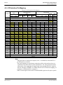
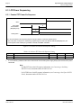
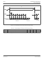
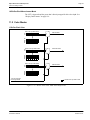
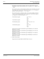
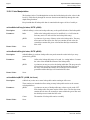
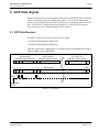
The D-TFD panel uses a 256-bit bit chain to control the pixel/FPSHIFT (XSCL) positions
relative to the falling edge of the GPIO4 (RES) signal. A one in each bit indicates the
presence of a GCP pulse at that pixel/XSCL position. A zero indicates the absence of a GCP
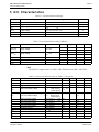
pulse. For D-TFD AC Timing required by the SED1376, see the SED1376 Hardware
Functional Specification, document number X31B-A-001-xx.
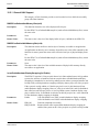
5.1 GCP Data Structure
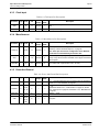
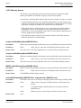
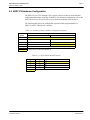
The SED1376 uses two registers to program the GCP Data:
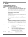
• D-TFD GCP Index Register (REG[28h]
• D-TFD GCP Data Register (REG[2Ch])
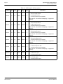
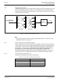
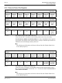
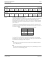
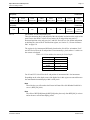
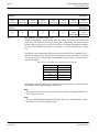
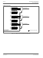
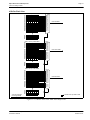
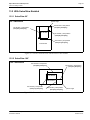
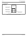
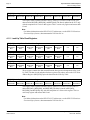
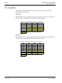
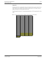
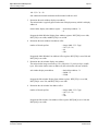
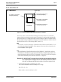
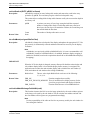
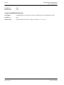
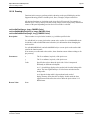
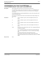
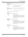
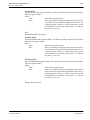
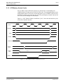
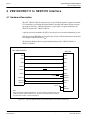
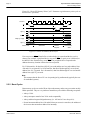
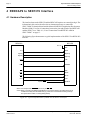
The 256-bit GCP data is organized into 32 8-bit data registers, each addressable by the DTFD GCP Index register (REG[28h]).
GCP index 00h
GCP index 01h
GCP index 1Fh
GCP data register window
GCP data register window
GCP data register window
b7 b6 b5
b0 b7
0
1
2
...
7
8
0
1
1
...
1
0
b0
GCP bit chain
b7
b0
...
256
...
0
GCP
falling edge
of RES
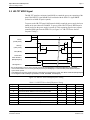
Figure 5-1: GCP Data
Connecting to the Epson D-TFD Panels
Issue Date: 00/07/12
SED1376
X31B-G-012-02