Download STEVAL-ISA081V1 - STMicroelectronics
Transcript
UM0984
User manual
STEVAL-ISA081V1 demonstration board based on a 12 V / 1 A
isolated flyback
Introduction
The purpose of this document is to provide information on the STEVAL-ISA081V1 switched
mode power supply (SMPS) demonstration board. The STEVAL-ISA081V1 is an isolated
SMPS capable of delivering a 12 W output over a wide input voltage range. It is designed for
a mains application focused on providing a cost-effective and space saving solution.
The STEVAL-ISA081V1 SMPS generates 12 V nominal output voltage using primary
regulation. This board is based on VIPer™26LD - a monolithic converter integrating a high
voltage MOSFET and PWM controller in one package.
This document contains a fundamental technical description of the demonstration board
(schematic diagram, PCB details, and bill of materials) as well as basic measurements
(load regulation, efficiency, standby behavior, EMI and thermal behavior data).
The last section of this document contains short recommendations on how to set different
output voltages in the range of 10 to 18 V and how to improve efficiency up to 86%.
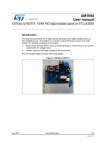
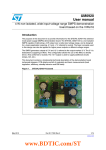
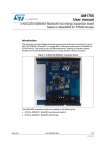
Figure 1.
June 2012
Demonstration board STEVAL-ISA081V1
Doc ID 17812 Rev 2
1/25
www.st.com
Contents
UM0984
Contents
1
Main characteristics . . . . . . . . . . . . . . . . . . . . . . . . . . . . . . . . . . . . . . . . . 5
2
Board connection . . . . . . . . . . . . . . . . . . . . . . . . . . . . . . . . . . . . . . . . . . . 6
3
Board description . . . . . . . . . . . . . . . . . . . . . . . . . . . . . . . . . . . . . . . . . . . 7
4
5
6
2/25
3.1
Schematic . . . . . . . . . . . . . . . . . . . . . . . . . . . . . . . . . . . . . . . . . . . . . . . . . . 7
3.2
Description of main components . . . . . . . . . . . . . . . . . . . . . . . . . . . . . . . . 9
3.2.1
The input section contains . . . . . . . . . . . . . . . . . . . . . . . . . . . . . . . . . . . . 9
3.2.2
The flyback converter consists of . . . . . . . . . . . . . . . . . . . . . . . . . . . . . . . 9
3.3
Transformer . . . . . . . . . . . . . . . . . . . . . . . . . . . . . . . . . . . . . . . . . . . . . . . 10
3.4
Layout . . . . . . . . . . . . . . . . . . . . . . . . . . . . . . . . . . . . . . . . . . . . . . . . . . . . 11
3.5
BOM . . . . . . . . . . . . . . . . . . . . . . . . . . . . . . . . . . . . . . . . . . . . . . . . . . . . . 13
Measurements . . . . . . . . . . . . . . . . . . . . . . . . . . . . . . . . . . . . . . . . . . . . . 15
4.1
Efficiency . . . . . . . . . . . . . . . . . . . . . . . . . . . . . . . . . . . . . . . . . . . . . . . . . 15
4.2
Standby . . . . . . . . . . . . . . . . . . . . . . . . . . . . . . . . . . . . . . . . . . . . . . . . . . 17
4.3
Load regulation . . . . . . . . . . . . . . . . . . . . . . . . . . . . . . . . . . . . . . . . . . . . 18
4.4
EMI . . . . . . . . . . . . . . . . . . . . . . . . . . . . . . . . . . . . . . . . . . . . . . . . . . . . . . 20
4.5
Temperature . . . . . . . . . . . . . . . . . . . . . . . . . . . . . . . . . . . . . . . . . . . . . . . 21
Application recommendations . . . . . . . . . . . . . . . . . . . . . . . . . . . . . . . . 22
5.1
Output voltage operating range . . . . . . . . . . . . . . . . . . . . . . . . . . . . . . . . 22
5.2
Improved efficiency . . . . . . . . . . . . . . . . . . . . . . . . . . . . . . . . . . . . . . . . . 23
Revision history . . . . . . . . . . . . . . . . . . . . . . . . . . . . . . . . . . . . . . . . . . . 24
Doc ID 17812 Rev 2
Document alternate name
List of tables
List of tables
Table 1.
Table 2.
Table 3.
Table 4.
Table 5.
Transformer windings . . . . . . . . . . . . . . . . . . . . . . . . . . . . . . . . . . . . . . . . . . . . . . . . .
Bill of materials . . . . . . . . . . . . . . . . . . . . . . . . . . . . . . . . . . . . . . . . . . . . . . . . . . . . . .
Settings and performance of demonstration board for different output voltages . . . .
Efficiency using a 60 V Schottky diode . . . . . . . . . . . . . . . . . . . . . . . . . . . . . . . . . . . .
Document revision history . . . . . . . . . . . . . . . . . . . . . . . . . . . . . . . . . . . . . . . . . . . . .
Doc ID 17812 Rev 2
. . . . 10
. . . . 13
. . . . 22
. . . . 23
. . . . 24
3/25
List of figures
UM0984
List of figures
Figure 1.
Figure 2.
Figure 3.
Figure 4.
Figure 5.
Figure 6.
Figure 7.
Figure 8.
Figure 9.
Figure 10.
Figure 11.
Figure 12.
Figure 13.
Figure 14.
4/25
Demonstration board STEVAL-ISA081V1 . . . . . . . . . . . . . . . . . . . . . . . . . . . . . . . . .
Input/output connection of SMPS . . . . . . . . . . . . . . . . . . . . . . . . . . . . . . . . . . . . . . . .
STEVAL-ISA081V1 circuit schematic . . . . . . . . . . . . . . . . . . . . . . . . . . . . . . . . . . . . .
Transformer construction . . . . . . . . . . . . . . . . . . . . . . . . . . . . . . . . . . . . . . . . . . . . . .
PCB layout - from top side TOP, BOT SMD, BOT copper . . . . . . . . . . . . . . . . . . . . .
Efficiency at 120 VAC and 230 VAC vs. output current . . . . . . . . . . . . . . . . . . . . . . .
Efficiency at full load (1 A) vs. input voltage . . . . . . . . . . . . . . . . . . . . . . . . . . . . . . . .
Standby power vs. input voltage . . . . . . . . . . . . . . . . . . . . . . . . . . . . . . . . . . . . . . . . .
12 V output load regulation . . . . . . . . . . . . . . . . . . . . . . . . . . . . . . . . . . . . . . . . . . . . .
3.3 V output load regulation . . . . . . . . . . . . . . . . . . . . . . . . . . . . . . . . . . . . . . . . . . . .
Output voltage at no load vs. the input voltage level . . . . . . . . . . . . . . . . . . . . . . . . .
EMI measurement regarding EN55022 Class 2 - left peak detector,
right AVG detector . . . . . . . . . . . . . . . . . . . . . . . . . . . . . . . . . . . . . . . . . . . . . . . . . . .
Thermal map of the board at 305 V AC on the input - left bottom side, right top side
Thermal map of the board at 85 V AC on the input - left bottom side, right top side .
Doc ID 17812 Rev 2
.....1
.....6
.....8
. . . . 11
. . . . 12
. . . . 15
. . . . 16
. . . . 17
. . . . 18
. . . . 19
. . . . 19
. . . . 20
. . . . 21
. . . . 21
UM0984
1
Main characteristics
Main characteristics
The main characteristics of the SMPS are listed below
●
●
Input:
–
VIN: 85 ~ 305 Vrms
–
frequency: 45 ~ 66 Hz
Output:
–
12 VDC ± 10%, 1 A (at 3.3 V not loaded)
–
3.3 VDC ± 4%, 100 mA
–
Maximum total output current of 1 A
●
Standby < 120 mW at 230 VAC
●
Short-circuit: protected
●
PCB type and size:
–
FR4
–
Single-sided 35 µm
–
32 x 90 mm
●
Isolation: isolated 4 kV / 8 mm
●
EMI: according to EN55022 Class B
Doc ID 17812 Rev 2
5/25
Board connection
2
UM0984
Board connection
The STEVAL-ISA081V1 demonstration board is shown in Figure 2 below, with input and
output locations.
Figure 2.
6/25
Input/output connection of SMPS
Doc ID 17812 Rev 2
UM0984
Board description
3
Board description
3.1
Schematic
A schematic diagram of the isolated flyback converter board prototype based on the
VIPER26LD is provided in Figure 3 on page 8.
Doc ID 17812 Rev 2
7/25
8/25
*
#
N&8
2
n
Doc ID 17812 Rev 2
6
6
2
$
344(2!
2
2
P&
6
#
#
6
N&
#
2
2
.!
&"
6$$
.#
'.$ '.$
,)-
#/-0
)#
$ 6IPER,$
.
$2!). $2!). $2!). $2!).
6
# #
6
2OPT
N&
#
N&
#
2
N&
6 #
$
3403( #
P&
#OPT
2
.!
42
%&
N&9
' ' ' '
#
N&
)#
,,!#
6
). 6/54
'.$
!-6
*
6
6
Figure 3.
66
$"
"3
,
XM(
#
Board description
UM0984
STEVAL-ISA081V1 circuit schematic
UM0984
3.2
Board description
Description of main components
The complete converter application consists of an input section and the flyback converter
itself.
3.2.1
The input section contains
Bridge diode rectifier (DB1)
The bridge diode rectifier is used to reduce the size of the input bulk capacitor.
Inrush current limiter (R1)
This component reduces the inrush current caused by the connection of the SMPS to
the mains (charging current of bulk capacitors) or by surge pulses. It is recommended
to use a wirewound resistor to get higher immunity against current spikes.
EMI filter (L1, C1, C2, C13)
This basic EMI pi-filter uses an X2 foil capacitor (C1), bulk capacitors (C2, C13) and
a CMC inductor (L1).
Input bulk capacitors (C2, C13)
These capacitors store energy when the input AC voltage is low. Their value respects
the minimum input voltage and output power. The maximum voltage of these capacitors
is 450 V for this design because the maximum input voltage is specified up to 305 VAC.
If the maximum input voltage of the application is lower (more often the value is 265
VAC), 400 V capacitors can be used.
3.2.2
The flyback converter consists of
VIPER26LD (IC1)
This device integrates a controller and high voltage power MOSFET in one package.
The controller works in current mode with a fixed frequency and in discontinuous mode
even at the lowest input voltage. Thanks to the built-in error amplifier, the VIPER26LD
can directly sense the auxiliary voltage via a voltage divider (R5, R6). Thanks to good
coupling of the auxiliary and secondary windings, the auxiliary voltage corresponds
well with the secondary voltage and can be used for feedback regulation. Mandatory
components for proper operation of the VIPer26 are VDD capacitor C4 and
compensation network R8, C6 and C7. Diode D2 provides auxiliary voltage to C4 and
the feedback voltage divider.
Note:
The voltage divider collecting feedback information for the FB pin is connected to the VDD
pin. The total resistance of this voltage divider has to be designed with respect to the
minimum charging current during startup and additional possible leakage currents (VDD
capacitor). The minimum charging current is 600 µA, the maximum leakage current through
the VDD capacitor can be theoretically in the range of several tens of µA. The total current
through the voltage divider is therefore set to 150 µA to guarantee enough margin for the
startup circuit.
Doc ID 17812 Rev 2
9/25
Board description
UM0984
Peak clamp (D1, R2, R3, C3)
This circuit absorbs energy from the voltage spike present after MOSFET turn-off. This
spike is generated by leakage inductance of the transformer. Alternatively, a Transil™based peak clamp can be used - for instance PKC-136. The application of this device
allows reducing standby consumption and it can also save some space on the board.
Secondary side (D3, C8, C11, R9, C9, IC2, C10)
The main secondary part is a rectifier consisting of D3 and C8. The C8 capacitor is
stressed by a high level peak current and therefore a low ESR capacitor is used. The
snubber circuit (optional) of D3 consists of C11 and R9. Thanks to the primary
regulation, no additional components are required.
A simple linear regulator to generate 3.3 V on the output can also be implemented. The
regulator (IC2) plays also the role of a bleeder - partly loading the output and keeping
the output voltage below limits at no load. In case IC2 is not assembled, some type of
bleeder (either a Zener diode or resistor) has to be applied in order to limit the
maximum output voltage at no load.
Note:
Components C13, DB1 and D3 appear with a suffix “A” on the PCB. This signifies that there
is an assembled alternative package on the board. The functionality of such a component is
the same as the basic component and therefore these components are not indicated in the
schematic visible in Figure 3.
3.3
Transformer
The transformer construction is designed in order to get good coupling between the auxiliary
and secondary to reach applicable load regulation even when the primary regulation is
used.
The transformer was developed in cooperation with WÜRTH ELEKTRONIK company and is
available under order number 760871131. The transformer specifications are as follows:
●
E20/10/6 - 60 kHz, voltage range 85 - 305 VAC
●
Core shape E20/10/6
●
Core Al 150 nH
●
Primary to secondary isolation 4 kV AC
Table 1.
10/25
Transformer windings
Wire
Wire
Inductance
Number
Wire
diameter
material
(µH)
of turns number
(mm)
Layer
Start
pin
Stop
pin
1
3
1
96
2
0.2
Cu2l
1394
Primary
2
7, 8, 9,
10
11, 12,
13, 14
10
4
0.3
TeX
15
12 V / 1 A
3
6
5
12
1
0.2
Cu2l
22
14.5 V / aux.
Doc ID 17812 Rev 2
Position
UM0984
Board description
Figure 4.
3.4
Transformer construction
Layout
The layout of the PCB is based on a single-sided FR4, with 35 µm thickness. The size of the
PCB is 32 x 90 mm. The distance between the primary and secondary side is higher than
8 mm, respecting the safety requirements for all standard applications. The layout of the
PCB is provided in Figure 5.
The layout was designed with respect to the following rules to achieve stable operation,
good efficiency and reduce EMI noise.
●
The power HF tracks are wide and short:
–
Transformer to IC1
–
Transformer to C13
–
IC1 to C13
–
Transformer to C8
–
C8 to D3
–
Transformer to D3
–
Peak clamp loop
●
The power and signal GND of VIPER26LD are separated and connected only in one
point close to the source pins
●
The EMI filter has been placed far from the transformer to avoid possible crosstalk of
EMI noise
Doc ID 17812 Rev 2
11/25
Board description
Figure 5.
12/25
UM0984
PCB layout - from top side TOP, BOT SMD, BOT copper
Doc ID 17812 Rev 2
UM0984
Board description
3.5
BOM
Table 2.
Bill of materials
Index
Quantity
Ref.
Value / generic part number
1
1
R1
5.1 Ω / 2 W
Wirewound
4.7 Ω / 2 W
Wirewound
51 kΩ / 5% / 0.25 W
1206
or
Package / class
2
2
R2, R3
3
1
R4
3.9 Ω / 5% / 0.1 W
0805
4
1
R5
150 kΩ /1% / 0.1 W
0805
5
1
R6
43 kΩ / 1% / 0.1 W
0805
6
0
R7
Not assembled
7
1
R8
10 kΩ / 5% / 0.1 W
8
0
R9
Not assembled
9
1
C1
100 nF / 305 VAC / X2
18 x 5 x 11 RM 15
10
1
C2
10 µF / 450 V
D12.5 x 20 RM 5
11
1
C3
470 pF / 200 V
1206
12
1
C4
10 µF / 35 V / 105 °C
D5 x 11 RM 2
13
1
C5
2.2 nF / 50 V
0805
14
1
C6
1 nF / 50 V
0805
15
2
C7, C10
100 nF / 50 V
0805
16
1
C8
470 µF / 35 V / low ESR
D10 x 20 RM 5
17
1
C9
330 nF / 50 V
0805
18
0
C11
Not assembled
19
1
C12
1 nF / 250 VAC / 4 kV / Y1
20
0
C13
Not assembled
21
1
C13A
22
1
23
Manufacturer
0805
EPCOS
RM 12
22 µF / 450 V
D16 x 20 RM 5
L1
CMC 2 x 10 mH
UU9.8, RM 8 x 7
EPCOS
1
T1
EF20 - 1.41 mH
EF20
WÜRTH ELEKTRONIK
24
0
DB1
Not assembled
25
1
DB1A
26
1
27
1 A / 800 V / bridge
SO-DIL
D1
STTH1R06A
SMA
1
D2
1N4148
MINIMELF / SOD80
28
0
D3
Not assembled
29
1
D3A
STPS2H100U
SMB
STMicroelectronics
30
1
IC1
VIPER26LN
SO16N
STMicroelectronics
31
1
IC2
L78L33AC
SO8N
STMicroelectronics
Doc ID 17812 Rev 2
STMicroelectronics™
13/25
Board description
Table 2.
UM0984
Bill of materials (continued)
Index
Quantity
Ref.
32
1
J1
Screw terminal 2 pos.
RM 5 mm
33
1
J2
Screw terminal 3 pos.
RM 5 mm
14/25
Value / generic part number
Package / class
Doc ID 17812 Rev 2
Manufacturer
UM0984
Measurements
4
Measurements
4.1
Efficiency
Figure 6.
Efficiency at 120 VAC and 230 VAC vs. output current
Doc ID 17812 Rev 2
15/25
Measurements
Figure 7.
UM0984
Efficiency at full load (1 A) vs. input voltage
The output voltage efficiency depending on the output current of the 12 V output is displayed
in Figure 6. The 3.3 V output was not loaded for this measurement.
Figure 7 shows the efficiency of the SMPS at full load applied on the 12 V output (1 A, 3.3 V
output not loaded) depending on the different input voltages. A drop of efficiency at low input
voltage is mainly caused by an increase of the losses of the input inrush resistor and CMC.
The efficiency was calculated as the ratio between the output power and input power. The
input power was directly measured by power analyzer NORMA 4000. The output power was
calculated as the product of the output current and output voltage. The output voltage was
measured on the output connector by multimeter KEITHLEY 2000 and the current was
measured by multimeter FLUKE 189.
16/25
Doc ID 17812 Rev 2
UM0984
Measurements
4.2
Standby
Figure 8.
Standby power vs. input voltage
The standby behavior of the board is displayed in Figure 8. The blue line is the standby input
power of the fully assembled board. The red line is the standby input power of the board
without linear regulator L78L33 and with a 15 V Zener diode applied as a bleeder. The
typical input current of L78L33 is 3.5 mA which is approximately 40 mW of load present on
the secondary side.
The standby input power was directly measured by power analyzer NORMA 4000. The
output connection was kept open during the measurement.
Doc ID 17812 Rev 2
17/25
Measurements
4.3
Load regulation
Figure 9.
12 V output load regulation
UM0984
The load regulation of the 12 V output is displayed in Figure 9. The output voltage at no
output load is determined by the consumption of L78L33. If L78L33 is not implemented and
no other bleeder (Zener diode or resistor) is used, the output voltage rises.
The load regulation of the 3.3 V output is visible in Figure 10.
18/25
Doc ID 17812 Rev 2
UM0984
Measurements
Figure 10. 3.3 V output load regulation
The output voltage of the 3.3 V and 12 V output at no load depending on the input voltage is
visible in Figure 11.
Figure 11. Output voltage at no load vs. the input voltage level
Doc ID 17812 Rev 2
19/25
Measurements
4.4
UM0984
EMI
The conductive EMI test of the demonstration board is displayed in Figure 12. The AVG
detector is indicated on the left, the peak detector measurement is indicated on the right.
Figure 12. EMI measurement regarding EN55022 Class 2 - left peak detector, right AVG detector
20/25
Doc ID 17812 Rev 2
UM0984
4.5
Measurements
Temperature
The thermal map at full load, measured at 305 VAC and at 85 VAC, is displayed in Figure 13
and Figure 14. The ambient temperature was 25 °C.
Figure 13. Thermal map of the board at 305 V AC on the input - left bottom side, right top side
Figure 14. Thermal map of the board at 85 V AC on the input - left bottom side, right top side
Doc ID 17812 Rev 2
21/25
Application recommendations
UM0984
5
Application recommendations
5.1
Output voltage operating range
The demonstration board STEVAL-ISA081V1 was originally designed for output
specification 12 V / 1 A supplied from wide input range 85 to 305 VAC. With minimal
changes of components it is possible to set a different output voltage in the nominal output
voltage range of 10 to 18 V, keeping the output power capability. The only changes are in the
values of voltage divider R5, R6. The other components including the transformer remain
the same. Table 3 shows applicable values of the voltage divider for different nominal output
voltages. There is also visible an indicative value of output voltage at full and no load,
standby consumption and efficiency at full load measured on one sample.
Table 3.
Settings and performance of demonstration board for different output
voltages
VOUT (V)
nominal value
R5 (kΩ) R6 (kΩ)
VOUT (V) VOUT(V) IOUT (A)
VAUX (V)
no load full load at load
PIN (mW)
Eff. (%)
no load
10
150
56
10.90
9.70
1.20
12.2
100
83.0
12
150
43
13.10
11.80
1.00
15.0
112
84.1
15
150
33
15.90
14.75
0.80
18.6
170
83.9
18
91
16
18.90
17.80
0.67
21.8
270
83.7
The major limitation regarding the setting of the output voltages is the VIPer26 supply range
(VAUX column) and transformer design.
The supply voltage of VIPer26 has to be in the range of 11.5 to 23.5 V which consequently
limits the output voltage range using the same transformer.
There are theoretically several possible limiting factors caused by the transformer due
primarily to the turns ratio. The consequence of using a transformer designed for 10 V
output for an 18 V output voltage level is a higher voltage stress on the primary side switch.
Thanks to the VIPer26 which has implemented an 800 V MOSFET, there is still enough
margin even at 18 V on the output. The maximum drain source voltage measured at
305 VAC with 18 V set on the output was 700 V.
22/25
Doc ID 17812 Rev 2
UM0984
5.2
Application recommendations
Improved efficiency
The measured efficiency is about 84% at full output load and 230 VAC. This value can be
increased by simply changing the output Schottky diode. Please note that the original board
contains an STPS3H100 - 3 A / 100 V Schottky diode. This diode is universal - applicable
also up to 18 V output voltage. If only 12 V output is required, a 60 V Schottky diode can be
used.
An STPS5L60 - 5 A / 60 V Schottky diode in the SMC package was tested. The result
measured on one sample at 230 VAC is displayed in Table 4.
Table 4.
Efficiency using a 60 V Schottky diode
D3
VOUT (V) full load
IOUT (A) full load
Eff. (%)
VD3 (V) at 305 VAC
STPS3H100
11.80
1.00
84.1
56
STPS5L60
12.15
1.00
86.1
56
Doc ID 17812 Rev 2
23/25
Revision history
6
UM0984
Revision history
Table 5.
24/25
Document revision history
Date
Revision
Changes
25-Nov-2010
1
Initial release.
08-Jun-2012
2
Updated Figure 3, minor text corrections throughout document.
Doc ID 17812 Rev 2
UM0984
Please Read Carefully:
Information in this document is provided solely in connection with ST products. STMicroelectronics NV and its subsidiaries (“ST”) reserve the
right to make changes, corrections, modifications or improvements, to this document, and the products and services described herein at any
time, without notice.
All ST products are sold pursuant to ST’s terms and conditions of sale.
Purchasers are solely responsible for the choice, selection and use of the ST products and services described herein, and ST assumes no
liability whatsoever relating to the choice, selection or use of the ST products and services described herein.
No license, express or implied, by estoppel or otherwise, to any intellectual property rights is granted under this document. If any part of this
document refers to any third party products or services it shall not be deemed a license grant by ST for the use of such third party products
or services, or any intellectual property contained therein or considered as a warranty covering the use in any manner whatsoever of such
third party products or services or any intellectual property contained therein.
UNLESS OTHERWISE SET FORTH IN ST’S TERMS AND CONDITIONS OF SALE ST DISCLAIMS ANY EXPRESS OR IMPLIED
WARRANTY WITH RESPECT TO THE USE AND/OR SALE OF ST PRODUCTS INCLUDING WITHOUT LIMITATION IMPLIED
WARRANTIES OF MERCHANTABILITY, FITNESS FOR A PARTICULAR PURPOSE (AND THEIR EQUIVALENTS UNDER THE LAWS
OF ANY JURISDICTION), OR INFRINGEMENT OF ANY PATENT, COPYRIGHT OR OTHER INTELLECTUAL PROPERTY RIGHT.
UNLESS EXPRESSLY APPROVED IN WRITING BY TWO AUTHORIZED ST REPRESENTATIVES, ST PRODUCTS ARE NOT
RECOMMENDED, AUTHORIZED OR WARRANTED FOR USE IN MILITARY, AIR CRAFT, SPACE, LIFE SAVING, OR LIFE SUSTAINING
APPLICATIONS, NOR IN PRODUCTS OR SYSTEMS WHERE FAILURE OR MALFUNCTION MAY RESULT IN PERSONAL INJURY,
DEATH, OR SEVERE PROPERTY OR ENVIRONMENTAL DAMAGE. ST PRODUCTS WHICH ARE NOT SPECIFIED AS "AUTOMOTIVE
GRADE" MAY ONLY BE USED IN AUTOMOTIVE APPLICATIONS AT USER’S OWN RISK.
Resale of ST products with provisions different from the statements and/or technical features set forth in this document shall immediately void
any warranty granted by ST for the ST product or service described herein and shall not create or extend in any manner whatsoever, any
liability of ST.
ST and the ST logo are trademarks or registered trademarks of ST in various countries.
Information in this document supersedes and replaces all information previously supplied.
The ST logo is a registered trademark of STMicroelectronics. All other names are the property of their respective owners.
© 2012 STMicroelectronics - All rights reserved
STMicroelectronics group of companies
Australia - Belgium - Brazil - Canada - China - Czech Republic - Finland - France - Germany - Hong Kong - India - Israel - Italy - Japan Malaysia - Malta - Morocco - Philippines - Singapore - Spain - Sweden - Switzerland - United Kingdom - United States of America
www.st.com
Doc ID 17812 Rev 2
25/25


