1
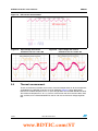
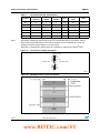
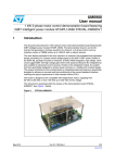
UM0926
User manual
STEVAL-ILL019V1 offline RGGB LED driver
demonstration board with high PF
Introduction
The STEVAL-ILL019V1 demonstration board was developed to drive high brightness and
power RGGB LEDs used in many different lighting applications. Thanks to RGGB LEDs, it is
possible to easily modify the color of the light, change the brightness level, implement
additional lighting features such as automatic color changes or a blinking mode, improve
lighting efficiency compared to standard lighting products and finally also achieve significant
energy savings. Typically, RGGB LED applications can be found as decorative lighting in
houses or hotels, as architectural lighting in stadiums, historic buildings, bridges and
monuments, as wall washing, shop lighting and in many other special lighting applications.
The STEVAL-ILL019V1 implements an innovative solution for driving multiple color RGGB
LEDs, where high Power Factor, safety isolation and individual regulation of LED brightness
are required. A constant current is set to 350 mA. Thanks to the microcontroller onboard,
the output channels are independently controlled by four PWM signals, allowing the
application users to set any color of the light or create automatic color effects. The
demonstration board is shown in Figure 1 and its ordering code is STEVAL-ILL019V1.
STEVAL-ILL019V1 main features
■
Constant LED current: 350 mA
■
4 channels for RGGB LEDs designed on the board
■
Line input voltage range: 88 V to 265 V AC
■
Load: 5 to 13 LEDs per each channel
■
32 W maximum RGGB LED power (wide input voltage range)
■
42 W maximum RGGB LED power (EU input voltage range)
■
Isolated SMPS
■
Individual regulation of RGGB brightness
■
EN55015 and EN61000-3-2 compliant
■
Double-sided PCB, 145 mm x 75 mm x 27 mm
Figure 1.
October 2010
STEVAL-ILL019V1 demonstration board
Doc ID 17274 Rev 1
1/25
www.st.com
www.BDTIC.com/ST
Contents
UM0926
Contents
1
Getting started with the STEVAL-ILL019V1 . . . . . . . . . . . . . . . . . . . . . . 5
1.1
Automatic color change mode . . . . . . . . . . . . . . . . . . . . . . . . . . . . . . . . . . 5
1.2
Manual color change mode . . . . . . . . . . . . . . . . . . . . . . . . . . . . . . . . . . . . 6
2
Design concept . . . . . . . . . . . . . . . . . . . . . . . . . . . . . . . . . . . . . . . . . . . . . 7
3
STEVAL-ILL019V1 measurements . . . . . . . . . . . . . . . . . . . . . . . . . . . . . . 8
3.1
PF, THD efficiency . . . . . . . . . . . . . . . . . . . . . . . . . . . . . . . . . . . . . . . . . . . 8
3.2
Output current for different number of LEDs . . . . . . . . . . . . . . . . . . . . . . 10
3.3
Maximum load capability . . . . . . . . . . . . . . . . . . . . . . . . . . . . . . . . . . . . . 11
3.4
Dimming . . . . . . . . . . . . . . . . . . . . . . . . . . . . . . . . . . . . . . . . . . . . . . . . . . 13
3.5
Input and output electrical waveforms . . . . . . . . . . . . . . . . . . . . . . . . . . . 13
3.6
Thermal measurement . . . . . . . . . . . . . . . . . . . . . . . . . . . . . . . . . . . . . . . 14
3.7
Standard EN61000-3-2 measurement . . . . . . . . . . . . . . . . . . . . . . . . . . . 15
3.8
EMI measurement (EN55015) . . . . . . . . . . . . . . . . . . . . . . . . . . . . . . . . . 16
4
Power transformer specifications . . . . . . . . . . . . . . . . . . . . . . . . . . . . . 17
5
Schematic diagrams . . . . . . . . . . . . . . . . . . . . . . . . . . . . . . . . . . . . . . . . 19
6
Bill of material . . . . . . . . . . . . . . . . . . . . . . . . . . . . . . . . . . . . . . . . . . . . . 21
7
References . . . . . . . . . . . . . . . . . . . . . . . . . . . . . . . . . . . . . . . . . . . . . . . . 24
8
Revision history . . . . . . . . . . . . . . . . . . . . . . . . . . . . . . . . . . . . . . . . . . . 24
2/25
Doc ID 17274 Rev 1
www.BDTIC.com/ST
UM0926
List of tables
List of tables
Table 1.
Table 2.
Table 3.
Table 4.
LED current vs. number of LEDs . . . . . . . . . . . . . . . . . . . . . . . . . . . . . . . . . . . . . . . . . . . . 11
Transformer design specifications . . . . . . . . . . . . . . . . . . . . . . . . . . . . . . . . . . . . . . . . . . . 18
Bill of material - STEVAL-ILL019V1 . . . . . . . . . . . . . . . . . . . . . . . . . . . . . . . . . . . . . . . . . . 21
Document revision history . . . . . . . . . . . . . . . . . . . . . . . . . . . . . . . . . . . . . . . . . . . . . . . . . 24
Doc ID 17274 Rev 1
www.BDTIC.com/ST
3/25
List of figures
UM0926
List of figures
Figure 1.
Figure 2.
Figure 3.
Figure 4.
Figure 5.
Figure 6.
Figure 7.
Figure 8.
Figure 9.
Figure 10.
Figure 11.
Figure 12.
Figure 13.
Figure 14.
Figure 15.
Figure 16.
Figure 17.
Figure 18.
Figure 19.
Figure 20.
Figure 21.
Figure 22.
Figure 23.
Figure 24.
Figure 25.
Figure 26.
Figure 27.
Figure 28.
Figure 29.
Figure 30.
4/25
STEVAL-ILL019V1 demonstration board . . . . . . . . . . . . . . . . . . . . . . . . . . . . . . . . . . . . . . . 1
Default RGGB LED load used for testing . . . . . . . . . . . . . . . . . . . . . . . . . . . . . . . . . . . . . . . 5
J3 connector with manual control circuitry . . . . . . . . . . . . . . . . . . . . . . . . . . . . . . . . . . . . . . 6
Different color settings using manual color control . . . . . . . . . . . . . . . . . . . . . . . . . . . . . . . . 6
STEVAL-ILL019V1 block diagram . . . . . . . . . . . . . . . . . . . . . . . . . . . . . . . . . . . . . . . . . . . . 7
STEVAL-ILL019V1 demonstration board used for measurements. . . . . . . . . . . . . . . . . . . . 8
Power Factor measurement . . . . . . . . . . . . . . . . . . . . . . . . . . . . . . . . . . . . . . . . . . . . . . . . . 9
Power Factor - zoom measurement . . . . . . . . . . . . . . . . . . . . . . . . . . . . . . . . . . . . . . . . . . . 9
Total Harmonic Distortion (THD) measurement . . . . . . . . . . . . . . . . . . . . . . . . . . . . . . . . . 10
Efficiency measurement . . . . . . . . . . . . . . . . . . . . . . . . . . . . . . . . . . . . . . . . . . . . . . . . . . . 10
Modified buck converter output current . . . . . . . . . . . . . . . . . . . . . . . . . . . . . . . . . . . . . . . 11
High PF flyback converter power capability for VIN = 88 V AC . . . . . . . . . . . . . . . . . . . . . . 12
High PF flyback converter power capability for VIN = 185 V AC . . . . . . . . . . . . . . . . . . . . . 12
PWM dimming 50% . . . . . . . . . . . . . . . . . . . . . . . . . . . . . . . . . . . . . . . . . . . . . . . . . . . . . . 13
PWM dimming 10% . . . . . . . . . . . . . . . . . . . . . . . . . . . . . . . . . . . . . . . . . . . . . . . . . . . . . . 13
PWM dimming 1% . . . . . . . . . . . . . . . . . . . . . . . . . . . . . . . . . . . . . . . . . . . . . . . . . . . . . . . 13
PWM dimming 1% - zoom . . . . . . . . . . . . . . . . . . . . . . . . . . . . . . . . . . . . . . . . . . . . . . . . . 13
LED current measurement . . . . . . . . . . . . . . . . . . . . . . . . . . . . . . . . . . . . . . . . . . . . . . . . . 14
Input voltage and current waveforms for VIN = 110 V AC. . . . . . . . . . . . . . . . . . . . . . . . . . 14
Input voltage and current waveforms for VIN = 230 V AC. . . . . . . . . . . . . . . . . . . . . . . . . . 14
Thermal measurement on the STEVAL-ILL019V1 . . . . . . . . . . . . . . . . . . . . . . . . . . . . . . . 15
EN61000-3-2 compliance for input voltage 110 V AC . . . . . . . . . . . . . . . . . . . . . . . . . . . . 16
EN61000-3-2 compliance for input voltage 230 V AC . . . . . . . . . . . . . . . . . . . . . . . . . . . . 16
Quasi-peak measurement from 9 KHz to 30 MHz . . . . . . . . . . . . . . . . . . . . . . . . . . . . . . . 16
Average measurement from 150 KHz to 30 MHz . . . . . . . . . . . . . . . . . . . . . . . . . . . . . . . . 16
Transformer frame dimensions . . . . . . . . . . . . . . . . . . . . . . . . . . . . . . . . . . . . . . . . . . . . . . 17
Transformer winding description. . . . . . . . . . . . . . . . . . . . . . . . . . . . . . . . . . . . . . . . . . . . . 18
Winding position on the transformer . . . . . . . . . . . . . . . . . . . . . . . . . . . . . . . . . . . . . . . . . . 18
High PF flyback converter . . . . . . . . . . . . . . . . . . . . . . . . . . . . . . . . . . . . . . . . . . . . . . . . . 19
Four modified buck converters and microcontroller . . . . . . . . . . . . . . . . . . . . . . . . . . . . . . 20
Doc ID 17274 Rev 1
www.BDTIC.com/ST
UM0926
1
Getting started with the STEVAL-ILL019V1
Getting started with the STEVAL-ILL019V1
This section allows designers to quickly evaluate the board as the load and external
potentiometer connections (to manually control the color of the light) are described.
As already stated, the light color can be changed automatically or manually. The application
is set by default to automatic mode in case no potentiometer nor jumper is connected to the
board via the J3 connector (see Figure 1). In order to control each LED channel manually,
the potentiometers and jumper must be connected to the J3 connector. These two modes
are demonstrated in the following sections.
1.1
Automatic color change mode
First, the RGGB LEDs must be connected to the board via the output connector J6 (see
Figure 1). Four independent channels marked as CH1, CH2, CH3 and CH4 allow controlling
four independent LED strings. The LED anode must be connected to the plus (+) pin and the
LED cathode must be connected to the minus (–) pin, which is marked close to the
connector J6. The recommended minimum LED voltage for each channel is 15 V and the
maximum voltage is 40 V, in order to keep the LED current within ±5%. As the typical LED
forward voltage is 3.5 V, an LED string with 5 to 11 LEDs per channel must be used. The
designers must also take into account that the maximum output LED power is 32 W for wide
input voltage range (88 V to 265 V AC) and
42 W for EU input voltage range (188 V to 265 V AC). It is also possible to use only one, two
or three channels. A typical example of how the load with RGGB LEDs can be designed is
shown in Figure 2 which is also the default RGGB LED load used for measurements on the
STEVAL-ILL019V1demonstration board. In this case channel 1 has 6 green LEDs,
channel 2 has 8 red LEDs, channel 3 has 7 green LEDs and channel 4 has 9 blue
LEDs. This RGGB LED load is just for demonstration purposes and is not available
for ordering.
Figure 2.
Default RGGB LED load used for testing
Doc ID 17274 Rev 1
www.BDTIC.com/ST
5/25
Getting started with the STEVAL-ILL019V1
UM0926
The last step after the RGGB LED load connection is to supply the demonstration board
with the proper input voltage. The output light color is automatically changed as soon as the
input voltage is applied to the board via connector J1.
1.2
Manual color change mode
First connect the RGGB LED load to the STEVAL-ILL019V1 as described in the previous
section. Then connect the potentiometers to the J3 connector as demonstrated in Figure 3.
The control connector has three main purposes. Firstly, it is used in manufacturing to
connect the programming station and program the ST7 microcontroller. Secondly, it
connects up to four potentiometers to set the brightness of each LED string. For the RGGB
LED module, only three potentiometers are used because two green LED strings are driven
with the same brightness. The last feature on the connector is a “Mode selection Pin 9"
which is used to choose either automatic or manual mode. During automatic mode, pin 9 is
internally grounded. A positive voltage of 5 V must be connected to pin 9 (for example to use
the switch S) for the manual mode. The automatic mode does not require any action from
the user and changes the colors through the color spectrum. The manual mode keeps the
color stable based on the position of the potentiometers. The last step is to resupply the
board with the proper input voltage. The output light color can be manually tuned as
demonstrated in Figure 4. The external control circuitry is again used just for
demonstration purposes and is not available for ordering.
6/25
Figure 3.
J3 connector with manual control circuitry
Figure 4.
Different color settings using manual color control
Doc ID 17274 Rev 1
www.BDTIC.com/ST
UM0926
2
Design concept
Design concept
Figure 5 shows the STEVAL-ILL019V1 block diagram. Basically, the board consists of two
converters. The first one is in fact an AC/DC converter designed as an isolated high PF
flyback converter using the L6562A controller with the STP7NK80ZFP Power MOSFET as
a switch. The input voltage for this convertor can be between 88 V and 265 V AC and the
converter delivers up to 35 W for this wide input voltage range. The output voltage is set to
48 V. The high Power Factor flyback convertor was already designed separately for
demonstration purposes (ordering code is EVL6562A-35WFLB) and therefore all design
equations and calculations are described in AN2838 (see Section 7: References).
The second converter is in fact a constant current LED driver. It is a modified buck converter
designed as the constant current source recommended for proper LED driving using the
L6562A and STS4NF100 Power MOSFETs. Four independent DC/DC converters are
assembled on the board in order to drive independent RGGB LED strings. The
demonstration board for a modified buck converter was also developed (ordering code is
EVL6562A-LED) and this design concept is described in AN2983 (see Section 7:
References). All design equations for the modified buck converter are shown in AN2928
(see Section 7: References).
The color control and brightness regulation is provided by the PWM generator which has
four independent channels. Each PWM signal is connected to one modified buck converter
in order to set the required brightness level for each LED string. The PWM signal can be set
between 0% and 100% (no brightness or maximum brightness). The ST7FLIT15BF1M6
microcontroller assembled on the board provides the right PWM signals. Thanks to the
microcontroller, it is also possible to modify the light effects. The RGGB LED brightness can
be set manually, if the external potentiometers are connected to the board via the connector
J3.
Figure 5.
STEVAL-ILL019V1 block diagram
()'(0/7%2&!#4/2&,9"!#+#/.6%24%2
6).6TO
6!#
-/$)&)%$"5#+#/.6%24%2#(
TO,%$S
6
344(23
3403(!
)NPUTFILTER
0&CONTROLLER
,!$
340.+:&0
343.&
0&CONTROLLER
,!$
#(!..%,
#(!..%,
07-'%.%2!4 /2
CHANNELS
#(!..%,
-ICROCONTROLLER
34&,)4"&-
0 0 0 0
EXTERNALPOTENTIOMETERS
FORINDIVIDUALBRIGHTNESS
!-
Doc ID 17274 Rev 1
www.BDTIC.com/ST
7/25
STEVAL-ILL019V1 measurements
3
UM0926
STEVAL-ILL019V1 measurements
The most important parameters such as electrical behavior, thermal behavior, dimming
function, board power capability and standards (EN55015 and EN61000-3-2) were
measured on the STEVAL-ILL019V1demonstration board shown in Figure 6 and the results
are given in the following section.
Figure 6.
3.1
STEVAL-ILL019V1 demonstration board used for measurements
PF, THD efficiency
The power factor (PF) is shown in Figure 7 and Figure 8. Two RGGB LED loads are used for
this measurement. Firstly, the default load of 30 W RGGB LEDs (9 blue LEDs, 13 green
LEDs and 8 red LEDs) was used for the measurement and this load is shown in Figure 2.
The second load used for the measurement is 20 W RGGB LEDs (5 blue LEDs, 8 green
LEDs and 7 red LEDs). The power factor is 0.995 for the input voltage 110 V AC and 0.94 for
the input voltage 230 V AC (measured for 30 W load).
The total harmonic distortion (THD) measurement is demonstrated in Figure 9. THD is 8.5
for the input voltage 110 V AC and 14.1 for the input voltage 230 V AC (measured for 30 W
load).
The efficiency measurement for these two loads is shown in Figure 10. The efficiency is
approximately 75% for a 30 W load, which is in line with the estimation performance
because there are two converters (AC/DC and DC/DC) used in the design.
8/25
Doc ID 17274 Rev 1
www.BDTIC.com/ST
UM0926
STEVAL-ILL019V1 measurements
Figure 7.
Power Factor measurement
0OWER&ACTOR;=
0O WER&ACTOR
,%$S
,%$S
)NPUTVOLTAGE;6=
!-
Figure 8.
Power Factor - zoom measurement
0OWER&ACTOR;=
0O WER&ACTORZOOM
,%$S
,%$S
)NPUTVOLTAGE;6=
!-
Doc ID 17274 Rev 1
www.BDTIC.com/ST
9/25
STEVAL-ILL019V1 measurements
Figure 9.
UM0926
Total Harmonic Distortion (THD) measurement
4($;=
4($
,%$S
,%$S
)NPUTVOLTAGE;6=
!-
Figure 10. Efficiency measurement
%FFICIENCY;=
%FFICIENCY
,%$S
,%$S
)NPUTVOLTAGE;6=
!-
3.2
Output current for different number of LEDs
Thanks to the modified buck converter designed as the current source (additional feedback
resistors R56, R57, R58 and R59 in the design), it is possible to drive a variable number of
LEDs. The output constant current was checked for different numbers of LEDs connected to
the modified buck converter and the result is demonstrated in Table 1 and Figure 11. It is
recommended to have the output voltage between 15 V and 38 V in order to keep the output
LED current within approximately ±5%. An established number of LEDs follows the output
voltage recommendation and can be easily calculated as the LED forward voltage is
a typical parameter written in any LED datasheet.
10/25
Doc ID 17274 Rev 1
www.BDTIC.com/ST
UM0926
STEVAL-ILL019V1 measurements
Table 1.
LED current vs. number of LEDs
Number of
LEDs
4
5
6
7
8
9
10
11
12
13
ILED [mA]
390
362
351
346
346
348
350
351
355
357
VLED[V]
12.1
15
17.9
20.8
23.7
26.7
29.7
32.7
35.6
38.7
Figure 11. Modified buck converter output current
),%$;M!=
),%$
6,%$;6=
!-
3.3
Maximum load capability
One of the most important features regarding this reference design is its maximum power
capability because it limits the maximum number of LEDs connected to this board. The
power capability measurement for wide input voltage range is shown in Figure 12. The worst
case for the measurement is the minimum input voltage and therefore the board was tested
with the input voltage 88 V AC. The maximum power is limited by the high PF flyback
converter and so its power capability is measured separately (resistive load is connected to
the output of the high PF flyback converter - capacitor C10). Figure 12 shows that the output
voltage starts to decrease as soon as the load current reaches 0.7 A (blue waveform). As
indicated by the red waveform, the maximum output power is limited to 35 W. The inverted
buck converters are used as the second stage DC/DC converter and it is possible to
estimate their efficiency at 90% (also measured). Therefore maximum power capability of
the STEVAL-ILL019V1 for wide input voltage range is 32 W. Also, the Power MOSFET and
transformer temperature was checked after one hour with maximum load (35.8 W) with 88 V
input voltage (ambient temperature 25 °C). The Power MOSFET had a temperature of 61 °C
and the transformer had a temperature of 60 °C.
The maximum power capability for the EU voltage range (188 V to 265 V AC) is also
measured, refer to Figure 13. The high PF flyback converter is again measured separately
using a resistive load connected to the capacitor C10. In this case the maximum power limit
is above 35 W, as the minimum input voltage was set to 188 V AC. Finally, a higher input
voltage (188 V) compared to a wide input voltage range (88 V) means that the primary
current is lower (avoiding transformer saturation) and therefore the high PF converter is able
to deliver higher power to the load for the EU input voltage range. In this case, the maximum
Doc ID 17274 Rev 1
www.BDTIC.com/ST
11/25
STEVAL-ILL019V1 measurements
UM0926
power capability is limited by the temperature of the power components (mainly the
transformer and Power MOSFET). The maximum Power MOSFET and inductor temperature
was selected at 61 °C in order to have the same maximum temperature on the transformer
and Power MOSFET as that of the wide input voltage range. The temperature was
measured after 1 hour and the Power MOSFET had a temperature of 59 °C and the
transformer had a temperature of 61 °C for load power of 46 W. Efficiency for the inverted
buck converter can be again estimated at 90% and therefore maximum power capability of
the STEVAL-ILL019V1 for the EU input voltage range is 42 W as shown in Figure 13.
0/54;7=
6/54;6=
Figure 12. High PF flyback converter power capability for VIN = 88 V AC
6/54
0/54
)/54;!=
!-
Figure 13. High PF flyback converter power capability for VIN = 185 V AC
0/54;7=
6/54;6=
6/54
0/54
-AXIMUMPOWER
)/54;!=
!-
12/25
Doc ID 17274 Rev 1
www.BDTIC.com/ST
UM0926
3.4
STEVAL-ILL019V1 measurements
Dimming
The dimming function on the STEVAL-ILL019V1 was evaluated. One output channel
(channel 4 with 9 blue LEDs) of the inverted buck converter was measured. Figure 14 to
Figure 17 show the output LED current and voltage for brightness levels set to 50%, 10%
and 1%. Thanks to the inverted buck topology, the application can be also completely
switched off (no current flows to the LEDs), because the Power MOSFET is turned off by the
PWM signal (the L6562A controls the Power MOSFET).
Figure 14. PWM dimming 50%
Figure 15. PWM dimming 10%
Figure 16. PWM dimming 1%
Figure 17. PWM dimming 1% - zoom
3.5
Input and output electrical waveforms
The LED current measured for one channel (channel 4 with 9 blue LEDs) is shown in
Figure 18. The LED average current is 350 mA, the inverted buck converter switching
frequency is 189 kHz and the peak-to-peak LED current ripple is 57.8 mA.
Figure 19 shows the input current and voltage waveforms for the input voltage 110 V AC.
The default load of 30 W RGGB LEDs is used for this measurement. In this case the
STEVAL-ILL019V1 has PF = 0.995 and THD = 8.5%.
Figure 20 shows the input current and voltage waveforms for the input voltage 230 V AC.
The default load of 30 W RGGB LEDs is again used for this measurement. In this case the
STEVAL-ILL019V1 has PF = 0.94 and THD = 14.1%.
Doc ID 17274 Rev 1
www.BDTIC.com/ST
13/25
STEVAL-ILL019V1 measurements
UM0926
Figure 18. LED current measurement
Figure 19. Input voltage and current
waveforms for VIN = 110 V AC
3.6
Figure 20. Input voltage and current
waveforms for VIN = 230 V AC
Thermal measurement
Thanks to the thermal chamber and camera, the overall temperature for all the components
assembled on the STEVAL-ILL019V1 is easily detected. Figure 21 shows the thermal
behavior for ambient temperature 25 °C, input voltage 230 V AC and 30 W RGGB LED load.
The maximum temperature is 76.1 °C and it is measured on the sense resistors R35, R36,
R41 and R42, on the Power MOSFET T3 and T4 and also on the linear voltage regulator
IC3.
14/25
Doc ID 17274 Rev 1
www.BDTIC.com/ST
UM0926
STEVAL-ILL019V1 measurements
Figure 21. Thermal measurement on the STEVAL-ILL019V1
3.7
Standard EN61000-3-2 measurement
If the input power for a lighting application is above 25 W, then it is required to have an active
Power Factor Correction (PFC) circuit in the final application. The high PF flyback converter
with the L6562A controller (transition mode PFC controller) is perfectly suitable for such
applications. Thanks to this design approach, input voltage 110 V AC or input voltage 230 V
AC meets the standard EN61000-3-2 as seen in Figure 22 and Figure 23.
Doc ID 17274 Rev 1
www.BDTIC.com/ST
15/25
STEVAL-ILL019V1 measurements
UM0926
Figure 22. EN61000-3-2 compliance for input
voltage 110 V AC
Figure 23. EN61000-3-2 compliance for input
voltage 230 V AC
,IMIT
2EAL
0ERCENTAGEOFFUNDAMENTAL
HARMONIC;=
0ERCENTAGEOFFUNDAMENTAL
HARMONIC;=
,IMIT
2EAL
(ARMONICORDER
(ARMONICORDER
!-
3.8
!-
EMI measurement (EN55015)
The norm EN55015 (CISPR15) describes the limits and methods of measuring radio
disturbance characteristics of electrical lighting and similar equipment. The limits of the
mains terminal disturbance voltages for quasi-peak measurement for frequency range from
9 KHz to 30 MHz and the real measurement is demonstrated in Figure 24. The test was
performed with input voltage VIN = 230 V AC, 30 W RGGB LED load and the LED brightness
was set to maximum level. The limits of the mains terminal disturbance voltages for average
measurement for frequency range from 150 KHz to 30 MHz and the real measurement is
shown in Figure 25. These results comply with the standard EN55015 as shown in
Figure 24 and Figure 25.
Figure 24. Quasi-peak measurement
from 9 KHz to 30 MHz
16/25
Figure 25. Average measurement
from 150 KHz to 30 MHz
Doc ID 17274 Rev 1
www.BDTIC.com/ST
UM0926
4
Power transformer specifications
Power transformer specifications
Transformer type:
●
Winding type: layer
●
Core type: ER30
●
Coil former: horizontal type, 9 + 9 pins (see dimensions in Figure 26)
●
Mains insulation: 4 KV
Figure 26. Transformer frame dimensions
Electrical specifications for the transformer:
●
Converter topology: flyback, TM mode
●
Ferrite material PC40 or similar for SMPS
●
Min. operating frequency: 36 kHz
●
Inductance factor approximately Al = 90 nH; air gap in central leg
●
Primary inductance 1.61 mH
●
Primary winding N1 + N2 = 134 turns
Doc ID 17274 Rev 1
www.BDTIC.com/ST
17/25
Power transformer specifications
Table 2.
Note:
UM0926
Transformer design specifications
Winding
Layer
sequence
Start pin
number
Finish pin
number
Turns
Wire diameter
(mm)
Side
N1
5
3
1
67
0.4
Primary
N2
2
5
3
67
0.4
Primary
N3
1
8
7
13
0.2
Primary
N4
3
17, (18)
14, (15)
33
2*0.4
Secondary
N5
4
11
12
17
0.2
Secondary
N6
9 - over core
8
8
1
Cu foil
Shielding
Intersperse winding N3, N5 through as much of the winding area as possible in order to
reduce the leakage inductance (since these windings do not completely fill a layer, the
winding should be spaced evenly across the layers).
Each layer of windings N1 and N2 must be isolated by a single layer of Mylar® Tape.
Figure 27. Transformer winding description
42 .
.
0RIMARYSIDE
.
3ECONDARYSIDE
.
.
!-
Figure 28. Winding position on the transformer
18/25
Doc ID 17274 Rev 1
www.BDTIC.com/ST
*
#
N&
8
!
&
#
XM( !
,
$"
#
n
"#3-$
N&
8
#
N&
2
N&
6
2
2
N&
2
2 #
2
2
2
)# ,!$
).6 6##
#O MP '$
-ULT '.$
#3 :#$
2
2
#
#
P&
0#"
/)
2
4,!)$
)#
6 2
2
# 2
2
$
.
$
.
6
2 #
6
!-
$ # # M& 6 M& ": 6#
$
344(! 6
)#
6
6
,-!#$4
,,!#$4
6 6
). /54
). /54
)#
'
$
#
'.$
#
' ' ' #
#
# N&
N& N&
N&
6
344(23 6
2
4":6#
34 0 .+:&0 $
2 22
2
2
6
. $
2
N&
# 42 0+%!
$
$ 344(25
5
# N& 9
UM0926
Schematic diagrams
Schematic diagrams
Figure 29. High PF flyback converter
Doc ID 17274 Rev 1
www.BDTIC.com/ST
19/25
Schematic diagrams
UM0926
Figure 30. Four modified buck converters and microcontroller
6
)# ,!$
).6 6
##
#OMP '$ -ULT '.$ N& 2 #3 :#$ #
2
6
#
N&
# N&
N& #
N& #
N& #
N& #
0/4
6
0/4
)#
34&,)4"&&-
633
/3#0##,+ ).
6$$
/3#0#
2ESET
0!( 3,4)#
33!).0"
0!(3!4)#
3#+!).0"
0!(3!407-
-)3/!).0"
0!(3!407-
-/3)!).0"
0!(3!407-
#,+).!).0"
0!!407-)##$!4!
!).0"
0!-#/)###,+
!).0"
0!(3 #/ -0/54
2
2
2
.
$
6
N& 6
,
$
N& 6
M( !
4
2
. $
2 #
2
P&
2
6
'2%%.
343.&
2
2
6
34 03(!
# # N&
, N&
$
#
6
N& 6
)# ,!$
M( ! 2%$
).6 6
##
343.&
#OMP '$ 2 4
-ULT '.$ . $
2 #3 :#$ 2
#
2
2
P&
#
*
6
2
2
P&
2
.
$
2
6
N&
)# ,!$
).6 6
##
#OMP '$ -ULT '.$ #3 :#$ -ODE SELE CTION
'.$AU TOMATIC6MANUAL
2
#
P&
.
. $
# 3403(!
# # N&
2
$
6
.
$
2
#
6
# N& 6 $
2 4
. $
2
,
N& 6
M(! ",5%
343.&
2
#
2
P& #
2
2
P&
.
$
6
6
*
)# ,!$
).6 6
##
#OMP '$ -ULT '.$ #3 :#$ .
$
3403(!
#
2 # N&
$
#
N& 6
2 4
. $
2
#
34 .&
343
2
2
P& #
3403(! #
N&
,
6
M ( ! '2%%.
2
2
P&
.
$
!-
20/25
Doc ID 17274 Rev 1
www.BDTIC.com/ST
UM0926
Bill of material
6
Bill of material
Table 3.
Bill of material - STEVAL-ILL019V1
I
Q
Reference
Part
Type
Manufacturer
1
1
C1
220 nF / ~305 V AC X2 capacitor
EPCOS
B32923C3224M
2
1
C2
150 nF / ~305 V AC X2 capacitor
EPCOS
B32922C3154M
3
1
C3
470 nF / ~305 V AC X2 capacitor
EPCOS
B32923C3474M
4
1
C4
2.2 nF / 63 V
0805 SMD capacitor
5
1
C5
220 nF / 63 V
0805 SMD capacitor
6
C6, C12, C13,
C14, C15, C19,
C20, C23, C24,
C25, C28, C29,
100 nF / 63 V
23
C30,C33, C34,
C35, C38, C39,
C40, C41, C42,
C43, C45
0805 SMD capacitor
7
2
C7, C11
47 µF / 35 V
Electrolytic capacitor
8
1
C8
330 pF / 63 V
0805 SMD capacitor
9
2
C9, C10
1 mF / 63 V
Electrolytic capacitor EPCOS
B41821F8108M
10
1
C16
2.2 µF / 25 V
1206 ceramic
capacitor X7R
12063C225KAT2A
11
1
C17
4.7 µF / 63 V
Electrolytic capacitor
12
1
C18
1 nF / 250 V AC
Y1 capacitor
13
8
C21, C22, C26,
C27, C31, C32, 330 pF / 63 V
C36, C37
0805 SMD capacitor
14
1
C44
10 nF / 63 V
0805 SMD capacitor
15
1
DB1
1 A / 250 V
Diode bridge SMD
16
1
D1
P6KE300A
Transil™
unidirectional 300 V
STMicroelectronics
P6KE300A
17
1
D2
STTH1R06U
1 A / 600 V
ultrafast diode
STMicroelectronics
STTH1R06U
AVX
Ordering code
Murata Manufacturing
DE1E3KX102MA5B
Co., Ltd.
D3, D7, D8, D9,
D11, D13, D15,
1N4148
18 15 D17, 18, D19,
D20, D22, D23,
D24, D25
150 mA / 75 V
universal diode
19
1
D4
STTH3R02S
3 A / 200 V
ultrafast diode
STMicroelectronics
STTH3R02S
20
1
D5
STTH102A
1 A / 200 V
ultrafast diode
STMicroelectronics
STTH102A
Doc ID 17274 Rev 1
www.BDTIC.com/ST
21/25
Bill of material
Table 3.
UM0926
Bill of material - STEVAL-ILL019V1 (continued)
I
Q
21
1
D6
22
4
D10, D12, D14,
STPS1H100A
D16
1 A / 100 V Schottky
STMicroelectronics
diode
23
1
D21
BZV55C30
30 V Zener diode
(SOD80)
24
1
F1
2.5 A / 250 V
Fuse
25
1
F1
Fuse socket
26
5
H1, H2, H3, H4,
Screw
T1HEAT
Screw 3 x 6 mm
27
4
H11, H22, H33,
Column distance
H44
15 mm
28
5
IC1, IC5, IC6,
IC7, IC8
L6562AD
PFC controller
STMicroelectronics
L6562AD
29
1
IC2
TL431AID
Programmable
voltage reference
STMicroelectronics
TL431AID
30
1
IC3
L78M15ACDT
Linear voltage
regulator
STMicroelectronics
L78M15ACDT
31
1
IC4
L78L05ACD13TR
Linear voltage
regulator
STMicroelectronics
L78L05ACD13TR
32
1
IC9
ST7FLIT15BF1M6
Microcontroller
STMicroelectronics
ST7FLIT15BF1M6
33
1
J1
ARK120/2
Input connector
34
2
J3, J6
S1G40
Control connector
40-pin
35
1
L1
B82732F2451B001
Frame core chokes
2 x 100 mH / 0.45 A
EPCOS
B82732F2451B001
36
4
L2, L3, L4, L5
MSS1260-105KLD
1 mH / 0.4 A
Coilcraft
MSS1260-105KLD
37
1
OI1
PC817B
Optocoupler
38
2
R1, R2
1.5 MΩ
1206 SMD resistor
39
2
R3, R6
22 KΩ
0805 SMD resistor
40
1
R4
9.1 KΩ
0805 SMD resistor
41
2
R5, R22
39 KΩ
0805 SMD resistor
42
3
R7, R20, R21
2.2 KΩ
0805 SMD resistor
43
2
R8, R9
220 KΩ
1206 SMD resistor
44
6
R10, R13, R27,
10 Ω
R33, R39, R45
0805 SMD resistor
45
2
R11, R23
0805 SMD resistor
46
6
R12, R18, R28,
1 KΩ
R34, R40, R46
22/25
Reference
Part
BZV55C15
47 KΩ
Type
Manufacturer
Ordering code
15 V Zener diode
(SOD80)
STPS1H100A
0805 SMD resistor
Doc ID 17274 Rev 1
www.BDTIC.com/ST
UM0926
Bill of material
Table 3.
Bill of material - STEVAL-ILL019V1 (continued)
I
Q
Reference
Part
Type
Manufacturer
Ordering code
47
2
R14, R15
1.3 Ω
1206 SMD resistor
48
1
R16
1.5 Ω
1206 SMD resistor
49
3
R17, R19, R54
4.7 KΩ
0805 SMD resistor
50
1
R24
3.9 KΩ
0805 SMD resistor
51
4
R25, R31, R37,
2.7 KΩ
R43
0805 SMD resistor
52
4
R26, R32, R38,
1.5 KΩ
R44
0805 SMD resistor
53
8
R29, R30, R35,
R36, R41, R42, 5.6 Ω
R47, R48
1206 SMD resistor
54
4
R49, R50, R51,
1.8 KΩ
R52
0805 SMD resistor
55
1
R53
390 KΩ
0805 SMD resistor
56
1
R55
10 KΩ
0805 SMD resistor
57
4
R56, R57, R58,
160 KΩ
R59
0805 SMD resistor
58
1
TR1
ER30 core
Specified in this
document
TDK
59
1
T1
STP7NK80ZFP
Power MOSFET
9 A / 800 V
STMicroelectronics
STP7NK80ZFP
60
1
T1HEAT
HEATSINK
61
4
T2, T3, T4, T5
STS4NF100
Power MOSFET
4 A / 100 V
STMicroelectronics
STS4NF100
Doc ID 17274 Rev 1
www.BDTIC.com/ST
23/25
References
7
8
UM0926
References
1.
STMicroelectronics, Application note AN2838, 35 W wide-range high power factor
flyback converter demonstration board using the L6562A; see www.st.com.
2.
STMicroelectronics, Application note AN2983, Constant current inverse buck LED
driver using L6562A, see www.st.com.
3.
STMicroelectronics, Application note AN2928, Modified buck converter for LED
applications, see www.st.com.
Revision history
Table 4.
24/25
Document revision history
Date
Revision
25-Oct-2010
1
Changes
Initial release.
Doc ID 17274 Rev 1
www.BDTIC.com/ST
UM0926
Please Read Carefully:
Information in this document is provided solely in connection with ST products. STMicroelectronics NV and its subsidiaries (“ST”) reserve the
right to make changes, corrections, modifications or improvements, to this document, and the products and services described herein at any
time, without notice.
All ST products are sold pursuant to ST’s terms and conditions of sale.
Purchasers are solely responsible for the choice, selection and use of the ST products and services described herein, and ST assumes no
liability whatsoever relating to the choice, selection or use of the ST products and services described herein.
No license, express or implied, by estoppel or otherwise, to any intellectual property rights is granted under this document. If any part of this
document refers to any third party products or services it shall not be deemed a license grant by ST for the use of such third party products
or services, or any intellectual property contained therein or considered as a warranty covering the use in any manner whatsoever of such
third party products or services or any intellectual property contained therein.
UNLESS OTHERWISE SET FORTH IN ST’S TERMS AND CONDITIONS OF SALE ST DISCLAIMS ANY EXPRESS OR IMPLIED
WARRANTY WITH RESPECT TO THE USE AND/OR SALE OF ST PRODUCTS INCLUDING WITHOUT LIMITATION IMPLIED
WARRANTIES OF MERCHANTABILITY, FITNESS FOR A PARTICULAR PURPOSE (AND THEIR EQUIVALENTS UNDER THE LAWS
OF ANY JURISDICTION), OR INFRINGEMENT OF ANY PATENT, COPYRIGHT OR OTHER INTELLECTUAL PROPERTY RIGHT.
UNLESS EXPRESSLY APPROVED IN WRITING BY AN AUTHORIZED ST REPRESENTATIVE, ST PRODUCTS ARE NOT
RECOMMENDED, AUTHORIZED OR WARRANTED FOR USE IN MILITARY, AIR CRAFT, SPACE, LIFE SAVING, OR LIFE SUSTAINING
APPLICATIONS, NOR IN PRODUCTS OR SYSTEMS WHERE FAILURE OR MALFUNCTION MAY RESULT IN PERSONAL INJURY,
DEATH, OR SEVERE PROPERTY OR ENVIRONMENTAL DAMAGE. ST PRODUCTS WHICH ARE NOT SPECIFIED AS "AUTOMOTIVE
GRADE" MAY ONLY BE USED IN AUTOMOTIVE APPLICATIONS AT USER’S OWN RISK.
Resale of ST products with provisions different from the statements and/or technical features set forth in this document shall immediately void
any warranty granted by ST for the ST product or service described herein and shall not create or extend in any manner whatsoever, any
liability of ST.
ST and the ST logo are trademarks or registered trademarks of ST in various countries.
Information in this document supersedes and replaces all information previously supplied.
The ST logo is a registered trademark of STMicroelectronics. All other names are the property of their respective owners.
© 2010 STMicroelectronics - All rights reserved
STMicroelectronics group of companies
Australia - Belgium - Brazil - Canada - China - Czech Republic - Finland - France - Germany - Hong Kong - India - Israel - Italy - Japan Malaysia - Malta - Morocco - Philippines - Singapore - Spain - Sweden - Switzerland - United Kingdom - United States of America
www.st.com
Doc ID 17274 Rev 1
www.BDTIC.com/ST
25/25