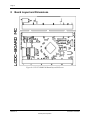
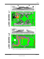
1
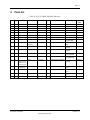
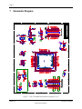
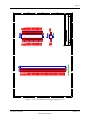
S5U13781R00C100 Reference Board User Manual Document Number: X94A-G-004-01 Status: Revision 1.0 Issue Date: 2012/03/26 SEIKO EPSON CORPORATION Rev. 1.0 Page 2 Evaluation board/kit and Development tool important notice 1. This evaluation board/kit or development tool is designed for use for engineering evaluation, demonstration, or development purposes only. Do not use it for other purpose. It is not intended to meet the requirement of design for finished product. 2. This evaluation board/kit or development tool is intended for use by an electronics engineer, and it is not a consumer product. The user should use these goods properly and safely. Seiko Epson dose not assume any responsibility and liability of any kind of damage and/or fire caused by usage of it. The user should cease to use it when any abnormal issue occurs, even during proper and safe use. 3. The parts used for this evaluation board/kit or development tool may change without notice. NOTICE No part of this material may be reproduced or duplicated in any form or by any means without the written permission of Seiko Epson. Seiko Epson reserves the right to make changes to this material without notice. Seiko Epson does not assume any liability of any kind arising out of any inaccuracies contained in this material or due to its application or use in any product or circuit and, further, there is no representation that this material is applicable to products requiring high level reliability, such as, medical products. Moreover, no license to any intellectual property rights is granted by implication or otherwise, and there is no representation or warranty that anything made in accordance with this material will be free from any patent or copyright infringement of a third party. This material or portions thereof may contain technology or the subject relating to strategic products under the control of the Foreign Exchange and Foreign Trade Law of Japan and may require an export license from the Ministry of Economy, Trade and Industry or other approval from another government agency. All brands or product names mentioned herein are trademarks and/or registered trademarks of their respective companies. S5U13781R00C100 Reference Board User Manual Revision 1.0 X94A-G-004-01 Issue Date: 2012/03/26 Seiko Epson Corporation Page 3 ©SEIKO EPSON CORPORATION 2012, All rights reserved. Table of Contents 1 Introduction ......................................................................................................................... 5 2 Features ............................................................................................................................. 6 3 Board Settings .................................................................................................................... 7 4 5 3.1 CNF[2:0] Configuration ................................................................................................................. 7 3.2 Jumper setting ............................................................................................................................... 8 3.3 Power Supply ................................................................................................................................ 9 3.3.1 VDDCORE ............................................................................................................................ 9 3.3.2 LED Back Light LED+/LED- Power Supply ........................................................................... 9 Connectors ........................................................................................................................10 4.1 J4 Host Interface Connector ....................................................................................................... 10 4.2 J5 Panel Interface Connector...................................................................................................... 10 4.3 J8 ~ J9 Connectors for Panel Connection ................................................................................ 11 Others ................................................................................................................................12 5.1 Quartz-Crystal Resonator for CLKI ............................................................................................. 12 5.2 SPI flash memory ........................................................................................................................ 12 6 Parts list .............................................................................................................................13 7 Schematic Diagram............................................................................................................14 8 Board Layout and Dimensions ...........................................................................................16 9 References ........................................................................................................................19 10 Change Record ..................................................................................................................20 X94A-G-004-01 Issue Date: 2012/03/26 S5U13781R00C100 Reference Board User Manual Revision 1.0 Seiko Epson Corporation Page 4 S5U13781R00C100 Reference Board User Manual Revision 1.0 X94A-G-004-01 Issue Date: 2012/03/26 Seiko Epson Corporation Page 5 1 Introduction This manual describes the setup and operation of the S5U13781R00C100 reference board. The reference board is designed as an evaluation platform for the S1D13781 Display Controller. The S5U13781R00C100 reference board has host controller connector, LCD panel connector, clock generator, SPI flash memory (16Mbit), power regulation circuit for S1D13781 core and DC/DC converter for LED back light. This user manual is updated as appropriate. Please check the Seiko Epson Website at http://www.epson.jp/device/semicon_e/product/lcd_controllers/index.htm for the latest revision of this document before beginning any development. We appreciate your comments on our documentation. Please contact us via email at [email protected]. X94A-G-004-01 Issue Date: 2012/03/26 S5U13781R00C100 Reference Board User Manual Revision 1.0 Seiko Epson Corporation Page 6 2 Features The S5U13781R00C100 reference board includes the following features: QFP 100pin S1D13781F00A100 Display Controller 2.54mm pitch vias for host bus interface header 2.54mm pitch vias for LCD panel header Connection area with 2.54mm pitch vias for header and FPC (0.5mm pitch 55 electrode) connector to connect LCD panel. On-board 24MHz crystal On-board voltage booster for LED back light (38V 60mA Maximum output at 5V input) On-board voltage regulator with 1.5V output from 3.3V/5.5V input for COREVDD and PLLVDD for the S1D13781 On-board 16Mbit SPI NOR FLASH standard memory S5U13781R00C100 Reference Board User Manual Revision 1.0 X94A-G-004-01 Issue Date: 2012/03/26 Seiko Epson Corporation Page 7 3 Board Settings 3.1 CNF[2:0] Configuration The S1D13781 has three configuration inputs, CNF[2:0], which are used to configure the S1D13781 host interface type as described in Table 3-1, Signal Allocation for Host Interface. The S5U13781R00C100 reference board defaults to the SPI interface (the default setting for CNF[2:0] = 111). Table 3-1 Signal Allocation for Host Interface S1D13781 Pin name Direct 16bit Mode 1 Direct 16bit Mode 2 Indirect 16bit Mode 1 Indirect 16bit Mode 2 Direct 8bit Indirect 8bit SPI CNF[2:0] 000 001 010 011 100 101 111 CS# CS# CS# CS# CS# CS# CS# SCS# WR# WR# RDU# WR# RDU# WR# WR# SCK RD# RD# RDL# RD# RDL# RD# RD# H UB# UB# WRU# UB# WRU# H H H LB# LB# WRL# LB# WRL# H H H AB0 TE TE TE TE AB0 TE TE AB1 AB1 AB1 P/C# P/C# AB1 P/C# Low AB[18:2] AB[18:2] AB[18:2] Low Low AB[18:2] Low Low DB0 DB0 DB0 DB0 DB0 DB0 DB0 SI DB1 DB1 DB1 DB1 DB1 DB1 DB1 SO DB[7:2] DB[7:2] DB[7:2] DB[7:2] DB[7:2] DB[7:2] DB[7:2] L DB8 DB8 DB8 DB8 DB8 TE L L DB[15:9] DB[15:9] DB[15:9] DB[15:9] DB[15:9] L L L Notes: “H” means direct connection to IOVDD “L” means direct connection to GND “Low” means internal pull-down for address bus active TE is determined by REG[22h] Display Settings Register bits 6-5 X94A-G-004-01 Issue Date: 2012/03/26 S5U13781R00C100 Reference Board User Manual Revision 1.0 Seiko Epson Corporation Page 8 3.2 Jumper setting The S5U13781R00C100 reference board includes jumpers which control the functions described in Table 3-2, Jumper settings. For jumper locations on the reference board, see Figure 3-1, Jumper Pin Locations. Table 3-2 Jumper Settings Function Jumper Settings Description Power supply for FLASH memory J1 1-2 2 3 Supply VDDIO to U2(FLASH-VCC) External power supply to U2(FLASH-VCC) GND CNF/RESET setting J2 1-2 3-4 5-6 7-8 CNF0 CNF1 CNF2 RESET Short: Short: Short: Short: Setting for back light LED regulator J3 1-2 3-4 5-6 7-8 Short: Short: Enables regulator Regulator output current +20mA Regulator output current +20mA Regulator output current +20mA Power supply for VDDIO / VDDDCDC J4 3 4 External power supply to VDDIO External power supply to VDDDCDC On board OSC setting J6 1-2 Short: Disable on board OSC On board OSC input J7 1 External clock input in case of OSC disable CNF0=0, Open: CNF0=1 CNF1=0, Open: CNF1=1 CNF2=0, Open: CNF2=1 RESET=0, Open: RESET=1 J2 J3 J4 J6 J1 Figure 3-1 Jumper Pin Locations S5U13781R00C100 Reference Board User Manual Revision 1.0 X94A-G-004-01 Issue Date: 2012/03/26 Seiko Epson Corporation Page 9 3.3 Power Supply The S5U13781R00C100 reference board is designed to supply VDDCORE (1.5V) and LED back light power (LED+/LED-) from the 2.7V to 5.5V input of J4-4 (VDD DCDC). The voltage output of 2.7V to 3.3V from J4-3 (VDDIO) is used for the U4 (S1D13781 Display Controller) power supply, D2 (LED indicator) and Y1(SG-310SCF 24MHz OSC). The power for U2 (M25P-16-VMN6P SPI flash memory) is supplied via J1-2 (FLASH-VCC). 3.3.1 VDDCORE VDDCORE (1.5V) is generated from U1 (BU15TD3WG Voltage regulator) and is used to supply power to COREVDD and PLLVDD of U4 (S1D13781 Display Controller). 3.3.2 LED Back Light LED+/LED- Power Supply The LED back light power supply (Maximum voltage between LED+ and LED- is 38V) is generated by U3 (TPS61161A voltage booster). The output current is set by J3 as described in Table 3-2, Jumper Settings. Connecting one of J3 3-4, J3 56 or J3 7-8 allows 20mA, connecting any two of them allows 40mA and connecting all of them allows 60mA output, maximum. Table 3-3 Power Supply for S5U13781R00C100 Power Supply Usage Voltage Range VDDIO Input IOVDD for U4 (S1D13781 Display Controller) Power supply for Y1 (SG-310SCF 24MHz OSC) Power supply for D2(SML-E12M8WT86 LED) 2.7V ~ 3.6V VDDDCDC Input Power supply for U1 (BU15TD3WG 1.5V LDO regulator) Power supply for U3(TPS61161A voltage booster) 2.7V ~ 5.5V FLASH-VCC Input Power supply for U2(M25P16-VMN6P SPI flash memory 2.7V ~ 3.6V VDDCORE Output COREVDD and PLLVDD for U4 (S1D13781 LCD controller) 1.5V (Fixed) LED+ / LED- Output LED back light power supply VDDDCDC ~ 38V Note: Do not short the power supply pins to any other pins. X94A-G-004-01 Issue Date: 2012/03/26 S5U13781R00C100 Reference Board User Manual Revision 1.0 Seiko Epson Corporation Page 10 4 Connectors The S5U13781R00C100 reference board has via for host interface and panel interface connectors (J4, J5, J8, J9 and J10). To locate of these connectors on the reference board, see Figure 4-1, Reference Board Connector Locations. J5 J4 J9 J10 J8 Figure 4-1 Reference Board Connector Locations 4.1 J4 Host Interface Connector The host interface pins of S1D13781 are connected to J4 of the S5U13781R00C100 reference board. See Figure 7-1, S5U13781R00C100 Schematic Diagram (1 of 2), and Figure 7-2, S5U13781R00C100 Schematic Diagram (2 of 2), for detailed pin allocation. 4.2 J5 Panel Interface Connector The panel interface pins of the S1D13781 are connected to J5 of the S5U13781R00C100 reference board. See Figure 7-1, S5U13781R00C100 Schematic Diagram (1 of 2), and Figure 7-2, S5U13781R00C100 Schematic Diagram (2 of 2), for detailed pin allocation. S5U13781R00C100 Reference Board User Manual Revision 1.0 X94A-G-004-01 Issue Date: 2012/03/26 Seiko Epson Corporation Page 11 4.3 J8 ~ J9 Connectors for Panel Connection J8 through J10 on the S5U13781R00C100 reference board are standard connectors used to implement suitable connection for various LCD panels. J8 is a 0.5mm pitch FPC connector (FH28-55S, bottom electrode type). See Figure 7-1, S5U13781R00C100 Schematic Diagram (1 of 2), and Figure 7-2, S5U13781R00C100 Schematic Diagram (2 of 2), for detailed pin allocation. X94A-G-004-01 Issue Date: 2012/03/26 S5U13781R00C100 Reference Board User Manual Revision 1.0 Seiko Epson Corporation Page 12 5 5.1 Others Quartz-Crystal Resonator for CLKI S5U13781R00C100 reference board includes Y1 (SG-310SCF 24MHz oscillator) for the CLKI input of the S1D13781. The output of the oscillator is disabled by connecting J6 1-2 and enabled by disconnecting. 5.2 SPI flash memory The S5U13781R00C100 reference board includes SPI NOR FLASH standard memory of 16Mbit capacity. It can be used as external image data storage for the S1D13781. S5U13781R00C100 Reference Board User Manual Revision 1.0 X94A-G-004-01 Issue Date: 2012/03/26 Seiko Epson Corporation Page 13 6 Parts list Table 6-1 S5U13781R00C100 Bill of Materials No. Qty Reference 1 1 U4 2 1 Y1 3 1 4 5 PKG Size Pin Part TQFP 14.0x14.0x1.7 100 S1D13781 LCD Controller EPSON 3225 3.2x2.5x1.2 4 SG-310SCF OSC 24MHz EPSON U3 QFN2x2 2.1x2.1x0.8 6 TPS61161ADRVT LED Driver TI 1 U1 SSOP5 3.1x3.0x1.25 5 BU15TD3WG Regulator LDO ROHM 1 L1 5050 5.0x5.0x2.0 2 VLCF5020T-220MR75-1 Inductor 22uH TDK 6 1 D1 3516 3.5x1.6.1.0 2 CRS04 SBD TOSHIBA 7 1 D2 1608 1.6x0.8x0.36 2 SML-E12M8WT86 LED ROHM 8 1 U2 SO8N 6x5 5.0x6.2x1.75 8 M25P16-VMN6P-ND SPI NORFLASH 16Mb Micron 9 1 J8 Bottom electrode 32.0x6.5x2.55 55 FH28-55S-0.5SH(05) FPC Connector 55P HIROSE 10 1 C18 2125 2.0x1.25x1.25 2 GRM21BB31H105KA12L Capacitor 1.0uF 50V/JB MURATA 11 1 C17 1608 1.6x0.8x0.8 2 GRM188B31E105KA75D Capacitor 1.0uF 25V/JB MURATA 12 2 C2,C14 1608 1.6x0.8x0.8 2 GRM188B31E474KA75D Capacitor 0.47uF 25V/JB MURATA 13 1 C16 1608 1.6x0.8x0.8 2 GRM188B31E224KA87D Capacitor 0.22uF 25V/JB MURATA 14 14 C1,C3,C4,C5, C6,C7,C8,C9, C10,C11,C12, C13,C15,C19 1005 1.0x0.5x0.5 2 GRM155B31C104KA87D Capacitor 0.1uF 16V/JB MURATA 15 7 R5,R6,R7,R8, R9,R10,R11 1608 1.6x0.8x0.45 2 RK73H1JTTD4702F Resistor 47K ohm KOA 16 1 R15 1608 1.6x0.8x0.45 2 RK73H1JTTD3300F Resistor 330 ohm KOA 17 3 R12,R13,R14 2125 2.0x1.25x0.5 2 RK73H2ATTD10R0F Resistor 10 ohm 1% KOA 18 4 R1,R2,R3,R4 1608 1.6x0.8x0.45 2 RK73Z1JTTD000 Resistor 0 ohm KOA X94A-G-004-01 Issue Date: 2012/03/26 Description Manufac turer S5U13781R00C100 Reference Board User Manual Revision 1.0 Seiko Epson Corporation Page 14 7 Schematic Diagram Figure 7-1 S5U13781R00C100 Schematic Diagram (1 of 2) S5U13781R00C100 Reference Board User Manual Revision 1.0 X94A-G-004-01 Issue Date: 2012/03/26 Seiko Epson Corporation Page 15 Figure 7-2 S5U13781R00C100 Schematic Diagram (2 of 2) X94A-G-004-01 Issue Date: 2012/03/26 S5U13781R00C100 Reference Board User Manual Revision 1.0 Seiko Epson Corporation Page 16 8 Board Layout and Dimensions Figure 8-1 S5U13781R00C100 Board Layout Silk Screen S5U13781R00C100 Reference Board User Manual Revision 1.0 X94A-G-004-01 Issue Date: 2012/03/26 Seiko Epson Corporation Page 17 Figure 8-2 S5U13781R00C100 Board Layout Top View Figure 8-3 S5U13781R00C100 Board Layout Bottom View X94A-G-004-01 Issue Date: 2012/03/26 S5U13781R00C100 Reference Board User Manual Revision 1.0 Seiko Epson Corporation Page 18 Figure 8-4 S5U13781R00C100 Board Dimensions (units: mm) S5U13781R00C100 Reference Board User Manual Revision 1.0 X94A-G-004-01 Issue Date: 2012/03/26 Seiko Epson Corporation Page 19 9 References Epson Research and Development, Inc., S1D13781 Hardware Functional Specification, document number X94A-A-001-xx. X94A-G-004-01 Issue Date: 2012/03/26 S5U13781R00C100 Reference Board User Manual Revision 1.0 Seiko Epson Corporation Page 20 10 Change Record X94A-G-005-01 Revision 1.0 - Issued: March 26, 2012 Release document as rev 1.0 S5U13781R00C100 Reference Board User Manual Revision 1.0 X94A-G-004-01 Issue Date: 2012/03/26 Seiko Epson Corporation International Sales Operations AMERICA ASIA EPSON ELECTRONICS AMERICA, INC. EPSON (CHINA) CO., LTD. 214 Devcon Drive, San Jose, CA 95112, USA Phone: +1-800-228-3964 7F, Jinbao Bldg., No.89 Jinbao St., Dongcheng District, Beijing 100005, CHINA Phone: +86-10-8522-1199 FAX: +1-408-922-0238 SHANGHAI BRANCH EUROPE EPSON EUROPE ELECTRONICS GmbH Riesstrasse 15, 80992 Munich, GERMANY Phone: +49-89-14005-0 FAX: +86-10-8522-1125 FAX: +49-89-14005-110 7F, Block B, Hi-Tech Bldg., 900 Yishan Road, Shanghai 200233, CHINA Phone: +86-21-5423-5577 FAX: +86-21-5423-4677 SHENZHEN BRANCH 12F, Dawning Mansion, Keji South 12th Road, Hi-Tech Park, Shenzhen 518057, CHINA Phone: +86-755-2699-3828 FAX: +86-755-2699-3838 EPSON HONG KONG LTD. Unit 715-723, 7/F Trade Square, 681 Cheung Sha Wan Road, Kowloon, Hong Kong. Phone: +852-2585-4600 FAX: +852-2827-4346 EPSON TAIWAN TECHNOLOGY & TRADING LTD. 14F, No. 7, Song Ren Road, Taipei 110, TAIWAN Phone: +886-2-8786-6688 FAX: +886-2-8786-6660 EPSON SINGAPORE PTE., LTD. 1 HarbourFront Place, #03-02 HarbourFront Tower One, Singapore 098633 Phone: +65-6586-5500 FAX: +65-6271-3182 SEIKO EPSON CORP. KOREA OFFICE 5F, KLI 63 Bldg., 60 Yoido-dong, Youngdeungpo-Ku, Seoul 150-763, KOREA Phone: +82-2-784-6027 FAX: +82-2-767-3677 SEIKO EPSON CORP. MICRODEVICES OPERATIONS DIVISION Device Sales & Marketing Dept. 421-8, Hino, Hino-shi, Tokyo 191-8501, JAPAN Phone: +81-42-587-5814 FAX: +81-42-587-5117 Document Code: X94A-G-004-xx First Issue March 2012 Revised March 2012 in JAPAN