1
SNIDS: FPGA-based Implementation of a Simple Network
Intrusion Detection System
Patrick Akl, Davor Capalija, Ivan Matosevic
Edward S. Rogers Sr. Department of Electrical and Computer Engineering
University of Toronto
{pakl, davor, imatos}@eecg.toronto.edu
ECE532S Course Project Group Report
April 13, 2006
Abstract
This report describes the implementation of SNIDS, a simple hardware network intrusion detection
system targeting FPGA devices. SNIDS snoops the traffic on the bus connecting the processor to the
Ethernet peripheral core and detects the Ethernet frames that match a predefined set of patterns indicating
malicious or disallowed content. SNIDS is based on a recently proposed architecture for high-throughput
string matching.
We implement the SNIDS using the Xilinx CAD tools and test its operation on an FPGA device.
Additionally, we implement software tools that enable automatic generation of a SNIDS core matching a
predefined set of patterns. We demonstrate the application of SNIDS within a realistic FPGA system-ona-chip connected to a small network.
1
Introduction
In this report, we describe the work done in the course of our ECE532 class project. We design and implement a simple network intrusion detection system (SNIDS) prototype using an FPGA platform.
SNIDS is implemented as an IP core that can be incorporated into systems-on-chip (SOC) based on
the Xilinx MicroBlaze processor that utilize the Ethernet Media Access Controller (EMAC) for network
access and the On-Chip Peripheral Bus (OPB) for interconnection. SNIDS implements a recently proposed
architecture for string matching [17]. This architecture delivers high throughput and efficient utilization
of chip area. Additionally, we argue that its specific memory utilization patterns make this architecture
especially suitable for implementation on modern FPGA devices featuring numerous small RAM blocks
that can be accessed independently.
1
SNIDS snoops the traffic on the OPB and detects the presence of patterns that indicate the presence of
malicious code or disallowed content in received Ethernet frames. If a suspicious pattern is detected in a
packet, SNIDS provides a unique identification code of the matched pattern to the processor.
We implement and synthesize the SNIDS core using the Xilinx EDK and ISE tools and test its operation
on a Xilinx Virtex II FPGA device. We develop software tools that enable us to automatically synthesize a
SNIDS core matching any predefined set of patterns, which can be provided in form of a simple text file.
For the purpose of testing the functionality of SNIDS and demonstrating its application in the context
of a realistic system, we develop a SOC based on the MicroBlaze and EMAC, which we then use to create
a rudimentary network consisting of two such systems. We successfully interconnect the SNIDS core with
the implemented SOC and demonstrate that it correctly recognizes Ethernet frames in which any of the
predefined patterns are present.
The remainder of this report is organized as follows. Section 2 presents a brief introduction into the area
of hardware-based network intrusion detection systems and describes the technique on which we base our
approach. Section 3 presents a high-level overview of the architecture of our implemented system. Section 4
provides a detailed description of the internal structure of SNIDS. Section 5 describes the software tools that
we have used in the course of the project. In Section 6, we present an overview of the testing and evaluation
of our system. In Section 7, we survey the related work in the area of hardware-based network intrusion
detection systems. Section 8 presents the conclusions and discusses the possible directions for future work.
Finally, we include two appendices that provide some additional details about the software structure of our
project and the bus interface of our system.
2
Background
2.1 Network Intrusion Detection Systems
Due to the increasing throughput of modern computer networks, as well as the constant emergence of new
security threats, effective network intrusion detection is becoming an increasingly challenging task. One of
the principal techniques for dealing with security threats are network intrusion detection systems (NIDS) that
operate by scanning the traffic on gateways that connect the vulnerable local area networks to the outside
2
world. A NIDS scans the header and payload of each transmitted network packet and filters out packets
suspected to be a part of an attempted intrusion or to carry some kind of disallowed content. The payload of
each packet is matched against a set of rules that specify various classes of potentially threatening content.
Such scanning is typically performed in conjunction with filtering at the TCP/IP layer, i.e. with the classic
network firewall functionality.
NIDS implementations in software are a well-studied area, in which the Snort system [13, 14] has
emerged as the de facto standard. The core of Snort is based on a database of rules, each of which specifies
an action to be performed when a packet satisfies a condition stated as a part of the rule. The rules refer to
the header as well as the payload of the packet. For example, the rule:
drop tcp any any -> 10.1.1.0/24 80 (content:"|00 01 86 a5|")
instructs the Snort NIDS to drop the packet sent from any IP address and any TCP port to the port 80
of any machine whose IP address matches the mask 10.1.1.0/24 and whose payload contains the sequence
of bytes in the quotation marks. Snort also supports other actions, such as alerting the system administrator
or logging the suspicious packets into a file. Although some of the payload matching rules are in form of
regular expressions, most of the rules consist of strings to be matched literally.
A NIDS must be able to process the traffic over the network connection in real-time without becoming
a performance bottleneck. Software NIDS implementations are no longer capable of handling the enormous
bandwidth provided by modern network connections [16]. This problem has motivated extensive research
into hardware implementations of intrusion detection systems in recent years. Several authors have investigated the possible ways of implementing hardware mechanisms for matching Snort rules. We survey their
work in Section 7. Aldwairi et al. [2] study the Snort rules and show that in practice, 87% of the rules contain
strings to match against the packet payload. In addition, they demonstrate that the string matching is the most
computationally intensive component of a Snort implementation. Therefore, the key issue in hardware-based
intrusion detection is the implementation of efficient string matching techniques in hardware.
The goal of our project is to implement the approach for hardware-based string matching recently proposed by Tan and Sherwood [17] using FPGAs. This approach is based on a modified version of the AhoCorasick string matching algorithm, which we describe in the following subsection.
3
2.2 The Bit-Split Aho-Corasick FSM
The Aho-Corasick algorithm [1, 17] constructs a finite state machine (FSM) for matching a given set of
strings. The string matching architecture that we describe in this report is based on constructing a set of
Aho-Corasick FSMs, to which we subsequently apply a technique called bit-splitting in order to enable their
efficient implementation in hardware. In this section, we provide an informal summary of the Aho-Corasick
algorithm and a description of the bit-splitting procedure.
The Aho-Corasick algorithm initially builds a directed tree whose root represents the initial state of
the FSM, and whose other nodes represent the states that correspond to a matched string or string prefix.
Let Sk be the node corresponding to the string c 1 c2 · · · ck , where ci is the i-th character in the string. Let
S0 → S1 → · · · → Sk be the path from the root node S0 to the node Sk . Then the edge Si−1 → Si
represents the transition taken by the Aho-Corasich FSM for the character c i during the matching of the
string c1 c2 · · · ck . If a subset of two or more strings shares a common prefix, then the paths from the root
to their corresponding nodes share a path prefix. For example, matching of the string c 1 c2 c3 d4 · · · dl , where
d4 6= c4 , would require adding a new path to the Aho-Corasick tree, which would however share the initial
state and the three subsequent states with the above mentioned path S 0 → S1 → · · · → Sk , because of a
common three-character prefix of the corresponding strings. Since the root node S 0 represents the initial
state, in which nothing has been matched so far, it is shared between all paths in the Aho-Corasick tree.
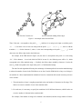
An example of an Aho-Corasick tree is shown in Figure 1(a). The tree corresponds to the set of strings
{abab, ac} over the alphabet {a, b, c}. The accepting states, i.e. the states corresponding to a fully matched
string, are shown in a darker color.
The second and final step in the Aho-Corasick algorithm consists of adding the so-called failure edges
to the FSM graph. Figure 1(b) shows the Aho-Corasick FSM for the set of strings {abab, abc} after adding
the backward edges. These edges represent the transitions that occur:
• When a prefix c1 · · · ci of a partially matched string c1 · · · ck is followed by a character different from
ci+1 , i.e. when a failure in matching occurs;
• When a new character is received after matching a full string.
In both cases, it is possible that the several last received characters correspond to a prefix of a different string.
4
(a) The Aho-Corasick tree
(b) The FSM after adding failure edges
Figure 1: An example Aho-Corasick FSM
Thus, if the state s corresponds to the prefix c 1 · · · ci , and there is no string in the input set with the prefix
c0 c1 · · · ci d, but there exists at least one string with the prefix c j cj+1 · · · ci d, 1 < j < i, then we add the
transition s → s0 for the character d, where s0 is the state corresponding to the prefix c j cj+1 · · · ck d. In all
other cases, the failure edge leads to the initial state.
For example, in the FSM shown in Figure 1(b), the state S 3 corresponds to the prefix aba of the string
abab. If the character c is received while the FSM is in state S 3 , the following state will be S5 , which
corresponds to the fully matched string ac. Similarly, the failure edges marked by character a lead to the
state S1 , which corresponds to the single-letter prefix a of both matched strings.
The Aho-Corasich algorithm efficiently takes advantage of common prefixes between the matched strings
to reduce the number of states in the FSM. However, an Aho-Corasick FSM built for a large set of strings is
not suitable for a direct implementation in hardware based on a transition table stored in memory, because
of two reasons:
1. The total number of states is roughly proportional to the total number of characters in all strings. This
leads to an excessive number of rows in the transition table.
2. For each state, it is necessary to specify the transitions for 256 different characters, which leads to an
excessive number of columns in the transition table.
For example, if the number of strings to be matched is one thousand, and the average number of charac5
ters per string is somewhat higher than ten, the number of states in the Aho-Corasick FSM can be expected
to be on the order of ten thousand. Thus, fourteen bits are necessary for encoding the FSM state. For this
number of states, it is necessary to have a transition table with ten thousand rows and 256 columns of 14-bit
values. Therefore, the total size of the transition table is on the order of several megabytes. The memory
necessary for storing such a large transition table cannot be fit onto a reasonably sized chip. Furthermore,
since the transition table must be read for each input character, the latency of such a large memory block
would lower the throughput of the FSM to an unacceptable level. Additionally, the transition table of an
Aho-Corasick FSM is typically sparse, since for most states, all but a handful of characters cause transitions
into the initial state or its direct descendants corresponding to single-character prefixes. Implementation of
the transition table in a single RAM block fails to take advantage of this sparsity.
The problem of excessive table height can be solved by dividing the set of input strings into multiple subsets and creating separate Aho-Corasick state machines for each set. Each partial FSM can be implemented
as a separate module, each using a significantly smaller and thus faster RAM block. However, the problems
of excessive table width and inefficient handling of the transition table sparsity still remain.
The latter problem of excessive table width can be solved using a technique called bit splitting, proposed
in a recent paper by Tan and Sherwood [17]. This technique splits the FSM into multiple FSMs, each of
which processes a subset of the eight bits of each input character. This reduces the table width, since for
each state, it is now necessary to specify only 2 k transitions, where k is the number of bits per bit-split
FSM. For example, if an FSM is bit-split into four FSMs, each of which takes as input two bits of the input
character, it is necessary to specify only 2 2 = 4 transitions per state. For reasons explained by Tan and
Sherwood [17], the optimal way of bit-splitting an Aho-Corasick FSM is to utilize four bit-split FSMs, each
of which matches two bits of the input character.
We describe the procedure for bit-splitting of Aho-Corasick FSMs using the example of the bit-split
machine that handles the least significant bits b 1 and b0 of the input character. The states of the bit-split FSM
correspond to sets of states of the original FSM. The initial state of each bit-split FSM corresponds to a set
whose only element is the initial state of the original FSM, i.e. {S 0 }. We partition the states following the
initial state S0 into four categories, depending on the two least significant bits of the character that causes the
transition from the initial state. The sets of the original FSM states containing the elements from each of those
6
four categories become the four states of the bit-split FSM to which its initial state transits for different values
of the two least significant bits of the input character. Subsequently, for each set of states {S i1 , . . . , Sin } and
each combination of bits b1 b0 , we define the next state as the set of all states {S j1 , . . . , Sjm } of the original
FSM such that some state Sik transits into some Sjl for some character c whose least significant bits are b 1 b0 .
The process is repeated iteratively, adding new sets of states of the original FSM into the bit-split FSM, until
a fixed point is reached, i.e. the procedure stops once all of the new transitions lead to already existing states
of the bit-split FSM. The construction of bit-split FSMs for other pairs of bits is performed analogously.
For arbitrary FSMs, this method may result in an exponential combinatorial explosion of the number of
states in bit-split FSMs. However, for Aho-Corasick FSMs, this is guaranteed not to be the case – the number
of states in each bit-split FSM is at most equal to the number of states in the original FSM. Furthermore,
for Aho-Corasich FSMs, it is guaranteed that each string is matched by the original FSMs if and only if it is
matched by all of the bit-split FSMs produced. The justification and more detailed discussion of these facts
can be found in the paper by Tan and Sherwood [17]. Their hardware string matching architecture, which
we implement in the course of our project, is based on splitting the input set of strings to be matched into a
number of subsets, each of which is matched by a single rule module. Each rule module is implemented as
an Aho-Corasick FSM bit-split into four tiles, as shown in Figure 6. Each input character is broadcast to all
rule modules in each cycle.
Within a rule module, each tile processes two bits of the input character. A rule module matches an input
string if and only if all of its tiles agree on matching in the same cycle. Each tile generates a bit-vector, called
its partial match vector (PMV), which contains the number of bits equal to the number of strings matched
by the rule module. The bit k of the PMV of a tile is set to one if and only if the k-th string is matched by the
tile in the current cycle. The match vector of the rule module is thus obtained as the logical AND of the four
PMVs. Each row of the transition table for a bit-split FSM contains the PMV for the corresponding state,
besides the next state for
The paper by Tan and Sherwood [17] contains an extensive discussion of the various possibilities for
partitioning the input set of strings across the rule modules and bit-splitting the FSMs across tiles. Their
conclusion is that the optimal solution is to use four-way bit-split FSMs with 16 strings per rule module
and 256 states per tile. With this approach, the state of a bit-split FSMs is encoded with 8 bits, and the
7
transition table of a tile has 256 rows. Each row of the transition table contains four 8-bit next state codes
plus a 16-bit PMV. Thus, a single tile requires a RAM block with 256 × 48 = 12, 288 bits. Hence, for ten
thousand input strings, roughly six hundred rule modules are necessary, each containing four 12kbit memory
blocks, totaling roughly four hundred kilobytes of total on-chip RAM. This represents a saving of an order
of magnitude over the earlier described straightforward Aho-Corasick FSM implementation. Furthermore,
small 12kbit memories can be implemented with a very low read latency, enabling a high clock speed and
thus a high throughput of the string matching hardware.
Tan and Sherwood target their architecture for application-specific chips, however we argue that FPGAs
are a suitable target as well. First, this massively parallel architecture can be easily mapped to an FPGA chip.
Second, FPGAs contain numerous small blocks of on-chip memory that can be accessed simultaneously, and
are thus suitable for implementing individual tiles of the rule modules. We provide a practical test of these
claims by implementing a working FPGA-based prototype of a simple network intrusion system based on
the described architecture.
3
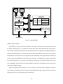
System Architecture Overview
Our system consists of the following components: a MicroBlaze soft processor [7], an Ethernet IP core, a
UART peripheral, and our hardware implementation of SNIDS, as shown in Figure 3. The components are
interconnected using the On-Chip Peripheral Bus (OPB) [8]. The Ethernet IP Core (EMAC) [9] implements
the Ethernet network layer and communicates with the off-chip physical Ethernet interface (PHY) [6]. The
UART peripheral [10] is used to output the necessary information to the PC terminal across an RS232 serial
interface.
We have considered two approaches to the system architecture. In this section, we describe and analyze
both approaches and explain the reasons for the choice of our design.
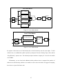
3.1 The Filtering SNIDS
With the first approach, the SNIDS hardware component is placed between the Ethernet IP core and the
processor. The SNIDS core forwards to the processor only those Ethernet frames that do not match any
of the malicious patters, thus effectively filtering the content received from the network. We refer to this
8
dlmb
ilmb
cntr
dlmb
O PB BUS
dlmb
cntr
MicroBlaze
O PB BUS
OPB_Intc
SNIDS IP
BRAM Block
OPB
Custom
Interface Logic
OPB
Interface
...
OPB_Emac
BRAM Block
OPB_Uartlite
PHY Device
RS 232
Figure 2: The filtering SNIDS
approach as the filtering SNIDS.
The system architecture of the filtering SNIDS is shown in Figure 2. The SNIDS core includes two OPB
interfaces, which connect it to the EMAC on one side and to the processor on the other. When an Ethernet
frame is received from the network, the EMAC interrupts the SNIDS core, which then reads the entire frame
and stores it into an internal buffer. Alternatively, the filtering SNIDS could be configured to poll the EMAC
instead of answering to the interrupts. The SNIDS string matching engine runs using the internally buffered
frame as input. Depending on whether the content of the frame is found to be malicious, the SNIDS either
drops the frame or interrupts the processor and transfers it via the second OPB bus.
3.2 Snooping SNIDS
With the second approach, which we refer to as the snooping SNIDS, the EMAC and the processor communicate directly via the OPB, as if the SNIDS was not present in the system. The architecture of the snooping
9
dlmb
cntr
ilmb
cntr
SNIDS IP
dlmb
ilmb
MicroBlaze
BRAM Block
O PB B US
OPB_Intc
OPB
Custom
Interface Logic
...
BRAM Block
OPB_Emac
OPB_Uartlite
PHY Device
RS 232
Figure 3: Snooping SNIDS
SNIDS is shown in Figure 3.
The SNIDS core is placed on the same OPB bus as the EMAC and snoops the communication between
the EMAC and the processor. It examines the content of the frame being transferred and stores the decision. The bus transactions between the processor and the EMAC are recognized by examining the addresses
placed on the OPB address bus. This approach assumes that the the Ethernet device drivers or the software
implementation of the network layer are augmented so that immediately after storing the frame in RAM, the
processor queries the SNIDS IP core about the safety of the frame. The SNIDS IP core replies with the ID of
the matched threat pattern, or a special code indicating that no patterns were matched and the frame is thus
safe. Depending on the threat ID received from SNIDS, the processor can discard the frame or take some
other action to handle the threat.
With the snooping SNIDS approach, every received frame is stored in RAM, including the malicious
ones. However, the malicious frames are detected and discarded before they are processed by any of the the
higher network layers, thus eliminating any detected threats.
10
3.3 Comparison of the Two Approaches
The advantages of the snooping SNIDS are its simpler design and lower cost in terms of chip resources. In
addition, it does not require extensive modifications of the existing SOC designs, since the SNIDS core is
connected as a simple slave component to the OPB bus. The only modification required is the addition of a
read transaction between the processor and the SNIDS upon receiving an Ethernet frame. On the other hand,
the filtering SNIDS includes two complex OPB interfaces and buffers for incoming and outgoing frames,
which require a significant chip area and might negatively affect the maximum operating frequency.
A disadvantage of the snooping SNIDS is that the processor is kept busy for each received frame, since
the decision to drop the frame is made only after it is stored into the memory. On the other hand, with the
filtering SNIDS, the processor is interrupted only if a safe frame is received.
In the course of our project, we have chosen the snooping SNIDS architecture due to its greater ease of
implementation.
4
SNIDS Architecture
The SNIDS core consists of two modules: the OPB snooping front-end and the string matching engine, as
shown in Figure 4. The OPB snooping front-end snoops the OPB bus and provides the input byte stream for
the string matching engine. The snooping front-end also stores the ID of the matched string generated by
the string matching engine and provides this information when queried by the processor. In this section, we
describe the architecture of these modules.
4.1 Architecture of the String Matching Engine
Figure 5 shows a string matching engine with four rule modules. Each input byte is broadcast to all rule
modules. Each rule module is responsible for matching a subset of the entire string set, as explained in
Section 2.2. In our SNIDS prototype, a module is responsible for matching a set of 16 input strings.
In order to assert that a string has been matched, a rule module generates a match vector, which is a
16-bit wide bit vector. Each bit in the match vector corresponds to one of the strings in the rule set matched
by the rule module, and is set if and only if the corresponding string has been matched after reading the last
11
SNIDS
Global OPB
signals
OPB snooping
front-end
String matching
engine
Input [7:0]
Slave OPB
signals
Enable
SID [6:0]
Figure 4: SNIDS
String Matching Engine
Rule Module 0
MV0 [15:0]
MV1 [15:0]
Rule Module 1
SID [6:0]
Input [7:0]
Encoder
MV2 [15:0]
Rule Module 2
Enable
MV3 [15:0]
Rule Module 3
Figure 5: String Matching Engine
input character.
The match vectors generated by the rule modules are inputs to the encoder, which translates the set of
match vectors into the numerical ID of the matched string. In the example in Figure 5, there are 64 matched
strings, which are assigned ID numbers from 1 to 64. The output of the encoder is the 7-bit string ID (SID).
The value of SID is zero if none of the strings were matched in the previous cycle, and equal to the number
12
Rule Module
Input [1:0]
Tile 0
PMV0 [15:0]
Input [3:2]
Tile 1
PMV1 [15:0]
Tile 2
PMV2 [15:0]
Tile 3
PMV3 [15:0]
MatchVector [15:0]
Input [7:0]
Input [5:4]
Input [7:6]
Enable
Figure 6: Rule module
of the matched string otherwise.
At a given clock cycle (i.e. at a given position in the input stream), at most one string can be matched
per rule module, and hence only a single bit in the match vector can be set. However, since different rule
modules represent independent Aho-Corasick FSMs, they can simultaneously match a string. For example,
if the input stream is defzabc, one rule module can match the string abc, whereas another module matches
the string zabc. In such cases, our system gives priority to the string matched by the rule module with the
lowest number. Since the set of input strings is sorted lexicographically prior to being partitioned across the
rule modules, the priority of strings is determined by their lexicographical order.
Figure 6 shows the implementation of a rule module. A rule module consists of four tiles, each of which
corresponds to a bit-split Aho-Corasick FSM, as described in Section 2.2. The input 8-bit byte stream is split
into four 2-bit streams. Each of the four tiles operates on one of the 2-bit streams. A single tile generates
only a partial match; a string is matched when the outputs of all four tiles agree. Therefore, the partial
match vectors generated by the tiles are AND-ed together bitwise to produce the full match vector of the rule
13
Tile
BRAM
Enable
Saved
State
DATA [47:0]
Address [7:0]
State Table
next_state [7:0]
next_states [7:0] [0..3]
Bit-split
input
data [47:0]
input [1:0]
pmv [15:0]
PMV
Partial Match
Vector
Figure 7: Tile
module. The width of the partial match vector is 16 bits, the same as the width of the full match vector.
The internal structure of a tile is shown in Figure 7. The bit-split FSM state table contains the information
on the next state and the partial match vector for each combination of the current state and the received 2-bit
input. The figure shows the design that we implement, with 256 states and a 16-bit partial match vector. Thus,
the state table contains 256 48-bit entries. Each 48-bit entry consists of four 8-bit IDs corresponding to the
four possible next states and a 16-bit partial match vector. The contents of the state tables are automatically
generated from the list of matched strings using a software tool that we describe in Section 5.3.
The current state of the bit-split FSM implemented by the tile is not stored in a separate register, but
exists in the form of the last value registered by the address input of the state table BRAM. Thus, the lower
32 bits of the state table output contain the four possible next states, one of which will be selected as the
current state in the next cycle. This selection depends on the input 2-bit value, and is performed by means
of a 4:1 byte multiplexer, whose four inputs are denoted as next states[7:0][3:0] in the figure. The
upper 16 bits of the state table output, which contain the partial match vector for the current state, are stored
in a dedicated register that drives the output of the tile.
The tile is equipped with the enable signal, whose purpose is to ensure correct operation in case the
input stream is not continuous. When the enable signal is disabled, the current state is stored into a dedicated
register named saved state, and the bit-split FSM remains in its current state for an indefinite period,
14
until the enable signal is asserted again. This feature is essential for the correct functioning of the snooping
SNIDS core, since the input bytes might not arrive from the OPB bus as a continuous sequence, as explained
in the following section.
4.2 The OPB Snooping Front-End
Upon the reception of a frame, the EMAC core interrupts the processor. The processor then issues a series
of bus transactions to fetch the frame length, as well as the frame itself from the EMAC. Alternatively, the
processor can poll EMAC to check for the presence of a frame, eliminating the need for the interrupt. In both
configurations, the transfers of the frame length and the frame itself take place using the same sequence of
I/O functions.
As a slave component on the OPB bus, the SNIDS core implements the following functions:
• Snooping of the frame length. The frame length read from the OPB is stored into a dedicated register
register, which is decremented every time a byte is fed to the string matching engine. Whenever the
counter reaches zero, the string matching engine is disabled. This enables the correct processing of
frames of arbitrary lengths, including those that are not 32-bit word-aligned.
• Snooping of the frame content. SNIDS snoops 32-bit words from the OPB bus and feeds them to the
string matching engine at the rate of one byte per cycle.
• Informing the processor on the matched string ID. After the completion of a frame transfer, the processor initiates a read transaction to the SNIDS. The SNIDS returns the ID of the matched string, or
zero if no strings were matched.
As an OPB slave, SNIDS does not initiate any bus transactions. It only snoops the OPB to capture the
frame length and the frame payload, and replies to the read transactions issued by the processor.
Figure 8 shows the structure of the OPB snooping front-end. Whenever the address decoder senses that
the EMAC is transferring the frame length to the processor, which indicates the start of the transmission of a
frame, the controller asserts the appropriate signals and the frame length is read from the data bus and used to
initialize the counter register. At this point, the controller also issues the reset signal to the string matching
engine in order to reset the FSMs.
15
OPB_xferAck
OPB_DBus
OPB_ABus
OPB_Select
OPB_Clk
Address
Decoder
0
Counter
1
2
3
Input [0:7]
Enable
Controller
Control signals
Matched string ID
1
0
0
Sln_xferAck
Matched
String ID
Sln_DBus[0:31]
Figure 8: OPB Snooping Front-end
After the frame length is captured, the contents of the frame are snooped from the data bus. The EMAC
keeps the frame content in a FIFO buffer. The processors can access the frame by reading a designated
address in the address range assigned to the EMAC. The processor transfers the frame from the Ethernet
FIFO to the data memory one word at a time. This is performed using a loop with a repetitive sequence of
load and store instructions, where every load is from the same FIFO address. SNIDS detects this address and
stores the value from the data bus to a special content register. The controller is responsible for selecting the
consecutive bytes from the content register and feeding them to the string matching engine. This is done by
means of an internal position register, which is not shown in Figure 8 for simplicity. Consequently, the string
matching engine takes four cycles to process a single word of the frame content. After a word is processed,
if the next one is not available, the controller stalls the string matching engine by lowering the enable signal.
16
Once the frame is transfered, the processor checks if the frame is safe, i.e. whether any of the strings
have been matched. The processor issues a read transaction to the SNIDS. The address decoder in the SNIDS
OPB interface senses that the processor is requesting the matched string ID. As a result, a dedicated control
signal is asserted and the content of the Matched String ID register is written to the slave OPB data bus. This
output is shown in the bottom part of the Figure 8.
The unused slave signals of the OPB interface are pulled to zero. When the SNIDS is not using the slave
data OPB lines, it sets all of its outputs to zero, as specified by the OPB standard.
In order to snoop the OPB bus and capture both the frame length and payload, the SNIDS must be able to
recognize the base address and the register offsets of the EMAC. These values are parameters of the SNIDS
core, which can be customized by the user for different versions of the EMAC.
Upon the reception of a four-byte word, it takes four cycles to properly process it and change the states of
the FSMs, as explained above. If the delay between two consecutive word transmissions is shorter than four
cycles, SNIDS will not process it fully. This would result in incorrect operation of the string matching engine.
This situation does not occur with the current system implementation, because the processor executes several
instructions between each two consecutive loads from the EMAC FIFO. To support faster transmission rates,
SNIDS would require the capability to buffer an entire frame. This would probably be required if the Ethernet
to memory transfer is implemented using DMA.
5
Software Tools
In this section, we describe the software tools used in the course of our project. We describe the tools
provided by Xilinx and other vendors, as well as the tools that we developed ourselves.
5.1 Provided Tools
We used the following off-the-shelf software tools:
1. Xilinx EDK: This tool was used to create both the software and hardware components of the MicroBlaze SoC system. In addition, EDK was used to encapsulate the SNIDS design in an IP core that can
be added to existing MicroBlaze-based designs.
17
2. Xilinx ISE: This tool is used by EDK to synthesize, place, and route the design onto the target FPGA.
Additionally, we used this tool for synthesis aimed at analyzing the performance of various modules.
3. Xilinx CoreGen: SNIDS utilizes the on-chip BRAMs to implement the bit-split FSMs. The CoreGen tool was used to generate and configure the netlists that implement the BRAM modules. We
created scripts that automatically invoke CoreGen to automate the netlist generation process, which
we describe in Section 5.2.
4. Mentor Graphics Modelsim: We used the Modelsim for the simulation testing of our system.
5. The g++ Compiler: The transition tables of the bit-split FSMs are generated using an automated tool
written in C++, which we compiled using the g++ compiler.
5.2 Generator of SNIDS Components
The SNIDS IP core can be customized in multiple ways. For example, it is possible to change the number of
rule modules and the set of matched strings. However, implementation of such customizable cores is not a
straightforward process, since changing the system parameters requires modifications of the Verilog source
code, in addition to changing parameters of Verilog modules. In order to enable customization of the SNIDS
core, we have developed a set of tools for automated generation of customized Verilog source code files.
Figure 9 shows the steps in generation of the SNIDS IP core. The software tools are shown using rounded
rectangles, and the files are shown using ordinary rectangles.
The given set of strings to be matched by the string matching engine is fed to the automated bit-split
FSM generator, which implements the algorithms described in Section 2.2. The output of this generator is
the number of required rule modules and the initialization files for the state tables of the tiles for each rule
module. These files are in the .coe format. They are used as inputs to the Xilinx CoreGen.
All the tiles used in the string matching engine are structurally fully identical; they differ only in the .coe
files used to initialize them. Other parameters of the BRAMs are the same. Initially, our plan was to use the
same module for all tiles, which would be parameterized by the initialization file. However, a limitation of
the CoreGen version 6.3 is that each BRAM module is tightly coupled with its initialization file. In other
words, for each state table with different contents, a separate module has to be generated. Consequently, we
18
Verilog
templates
Set of Strings
Verilog module
generator
Bit-split FSM
automatic
generator
Tiles
Rule_Modules
(Verilog)
Memory
initalization
files (COE)
BRAM
description
COREGEN
Top level
modules
(Verilog)
BRAM
Netlist
Pcore
Synthesis
Figure 9: Automatic SNIDS generator
had to generate a separate Verilog module for each rule module and each tile within each module.
For this purpose, we implemented shell scripts that create a number of Verilog files named rule module X,
where X varies from one to the total number of modules, as well as the files tile X Y, Y = 1, . . . , 4 for each
rule module X. These files are generated by modifying specific template Verilog sources that we wrote. Each
module tile X Y instantiates the corresponding BRAM module state table X Y. This module serves as the
wrapper for the BRAM netlist generated by the CoreGen.
The top-level modules instantiate the rule modules, the connecting logic, and the OPB snooping frontend. Together with the above mentioned automatically generated files, they are given as input to the EDK
environment, which is then used to produce the synthesizable SNIDS core. The details of the files and the
directory structure used to implement the SNIDS core in XPS are described in Appendix A.
19
5.3 Generator of Bit-Split FSMs
In this section, we describe the generator of bit-split finite state machines. The generator is a program written
in C++, whose input is the list of strings to be matched by the FSM, and the output is the set of transition
tables of the corresponding bit-split Aho-Corasick state machines, which is in the form of .coe files used by
CoreGen to initialize the BRAMs.
The program creates transition tables of multiple rule modules, each of which matches a subset of the
strings in the input file. The number of created rule modules depends on the number of input strings. Prior
to the construction of the tables, the input list of strings is sorted lexicographically in order to group strings
with common prefixes together. This increases the number of strings that can be fit into each module, since
the Aho-Corasick algorithm tends to minimize the number of states in the presence of common prefixes, as
described in Section 2.2.
We assume a 4-way bit-split Aho-Corasick state machine with up to 256 states and a 16-bit matching
vector. This places the upper bound of 16 strings per module (this number will be smaller than 16 if the
number of states exceeds 256 after adding less than 16 strings). Thus, a single module contains four BRAM
blocks, each storing 256 48-bit values, as explained in Section 2.2. For each module, the generator outputs
four .coe files, which are used for initializing the BRAM blocks.
The sorted list of the input strings is traversed using an algorithm whose simplified pseudocode is shown
in Figure 10. The input strings are added to the Aho-Corasick state machine until either the number of strings
exceeds the size of the match vector (16) or the number of states exceeds 256. The state machine is then split
into four bit-split FSMs. These steps are performed as described in Section 2.2. In the pseudocode shown in
Figure 10, we assume that these procedures are implemented by the functions add string to AC FSM,
which returns the number of newly added states, and split AC FSM, which returns a set of four transition
tables, each containing 256 48-bit values. A new rule module is created in each iteration of the outer do
loop.
6
Testing and Evaluation
In this section, we describe the testing and evaluation of our design.
20
L = array of input strings;
N = number of input strings;
lexicographical sort(L);
n = 0;
do {
n states = 0;
i = 0;
AC = empty FSM;
do {
n states += add string to AC FSM(L[n + i], AC);
i++;
} while (n + i < N && i < 16 && n states < 256);
tiles = split AC FSM(AC);
output COE files(tiles);
n += i;
} while (n < N);
Figure 10: Construction of the bit-split Aho-Corasick state machines
6.1 Simulation-Based Verification
We used simulation test benches to test the behavior of the implemented modules. We verified the functionality of the design incrementally, starting with the lower-level modules:
• Tiles constitute the lowest-level components in our design. The simulation of a tile was performed by
initializing the tile to a simple state machine, and observing the state transitions obtained given an input
stream of two-bit values. We also verified the correctness of the tile operation when the input stream
is not continuous and the enable signal is lowered to preserve the state during periods of inactivity.
• Rule Modules: each rule module instantiates four tiles and combines the output partial match vectors
of each tile into its match vector. Functional simulations of a rule module allowed us to verify the
correct matching of a string of 8-bit characters.
• The string matching engine instantiates multiple rule modules. We verified the functionality of the
string matching engine using different input patterns containing strings matched by different rule modules. We also varied the timing of the received bytes and the position of the strings, for the purpose of
further stress testing of the lower level modules.
21
• The SNIDS core instantiates the string matching engine and the snooping OPB interface. We simulated
this level of the design in a complete system simulation, which is described in the following subsection,
due to the complexity of modeling bus transactions using manually written test-benches.
After verifying the functional correctness of each of level in the design hierarchy, we synthesized it to
make sure that the behavioral description synthesizes into correct logic circuits. The synthesis process also
gave us hints about possible errors in the coding.
6.1.1
Complete System Simulation
In this phase, we simulated the system consisting of the following components:
• MicroBlaze processor, whose role is to send frames to the EMAC IP core.
• EMAC core, which receives frames from the processor and loops them back via the OPB bus.
• Interrupt controller, which enables the EMAC to interrupt the processor.
• SNIDS IP core, which snoops the bus to extract the frame payload and analyze it.
We wrote a simple program for the MicroBlaze that sends a high number of “malicious” frames, containing strings to be matched by SNIDS, as well as some “safe” frames, containing no such strings.
Initially, we planned to have the EMAC configured in loopback mode, so that the frames sent by MicroBlaze would be resent to it by the EMAC. Unfortunately, the loopback capability required a simulation
model for the external PHY Ethernet device, which we did not have. As a result, no received frames were
observed on the OPB, and the SNIDS core was unable to read anything from the bus. To solve the problem,
we modified the SNIDS OPB interface to snoop for the sent frames instead of the received frames. This
allowed us to verify the correctness of the OPB interface and to further test the functionality of the string
matching engine.
6.2 Real Hardware Tests
After verifying the functionality of the system using behavioral simulation, we performed multiple tests in
real hardware. We synthesized the above described system targeting the Xilinx Virtex-2 device and downloaded it to the Xilinx Multimedia board.
22
6.2.1
Test 1: EMAC Configured in Loopback Mode
To test the SNIDS using a single board, we configured the EMAC in loopback mode, so that all frames
sent to the EMAC are sent back to the processor. We sent a high number of safe and malicious frames and
verified that SNIDS returns the correct string ID, which is displayed on the PC terminal via the UART serial
interface. We tested this configuration with EMAC configured both in the interrupt-driven mode and in the
loopback mode. The MicroBlaze was configured with 32KB of on-chip data and instruction memory, so that
the free BRAMs could be used to implement the tiles of SNIDS. The SNIDS was configured with 14 strings
to be matched, and included four rule modules.
6.2.2
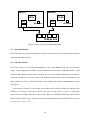
Test 2: Network of Boards
For the demo of our project, we interconnected two boards using a 10Mbps Ethernet hub, as shown in
Figure 11. Each of the systems running on the two boards consists of a MicroBlaze processor, a UART
controller for monitoring, an interrupt controller, a GPIO core, an EMAC core, and a SNIDS core. The
GPIO core implements communication between the processor and the DIP switch, which is used to control
the sending of packets from the board. For both systems, EMAC was configured in interrupt-driven mode.
Each board is configured with a different physical MAC address. MicroBlaze was again configured with
32KB of data and instruction memory. Each of the two boards is configured with a different SNIDS core,
implementing a different rule set. As in the previous tests, the SNIDS implementation contains four rule
modules.
The software running on each board is configured to send both malicious and safe frames to the second
board whenever a DIP switch is toggled. After a frame is received and completely buffered by the processor
in the interrupt service routine, a “read ID” OPB transaction is issued by the processor to the SNIDS, which
replies with the appropriate matched string ID (or zero in case no strings were matched). The string ID
is transferred via the serial port and printed on a HyperTerminal screen, which enables us to control the
correctness of the system operation.
23
Board 1
Board 2
FPGA
FPGA
PHY
PHY
DIP switch
DIP switch
10 Mbps Hub
Figure 11: Demo setup with two Multimedia boards
6.3 System Evaluation
In this subsection, we present the evaluation of our design in terms of the FPGA resource utilization and the
maximum achievable frequency.
6.3.1
BRAM Utilization
The critical resource for our SNIDS implementation are the on-chip BRAM blocks, since the maximum
number of rules supported by SNIDS is directly proportional to the number of BRAMs available. With
32KB of RAM dedicated to the processor memories, the base system without SNIDS (processor, Ethernet,
UART) uses 20 BRAMs. The Virtex-2 chip on the Multimedia board has the total of 56 BRAMs, the rest
being available for our core. With four BRAMs per rule module, this enables the implementation of nine
rule modules.
As described in Section 2.2, the bit-split state machine inside each tile includes the transition table
consisting of 256 entries. Each entry consists of four 8-bit next state codes, as well as a 16-bit partial
match vector, thus totaling 12,288 bits of data per tile. However, each BRAM block in the Virtex-2 FPGA
devices contains 18kbits of data. For these reasons, the maximum utilization of the BRAMs for our system
is 12, 288/(18 × 1024) = 67%.
24
6.3.2
Maximum Frequency
For the purposes of performance evaluation, we synthesized our SNIDS design targeting the Xilinx Virtex-4
xc4vfx140 device. This is a state-of-the-art Xilinx FPGA chip, which contains 552 BRAM blocks. For
the synthesis, we selected the speed grade -11. The results of the synthesis enabled us to estimate the
performance of SNIDS when synthesized on a modern high-end FPGA device. Furthermore, they enabled
us to investigate the behavior of our design when the number of rule modules is increased beyond what is
possible using the Virtex-2 device provided on the Multimedia Board.
The synthesis in the ISE reported a maximum frequency estimate of 263 MHz for one tile. We iteratively
lowered the timing constraint for the place and route process until we obtained the real maximum frequency.
We were able to place and route a tile with the operating frequency of 225MHz. The same applies for a
rule module. For a string matching engine consisting of four rule modules, we were able to obtain a postplace-and-route frequency of 217MHz. For 8 and 32 rule modules, the frequency dropped to 216MHz and
202MHz, respectively. We were not able to place and route the system with 64 rule modules, since ISE failed
to complete the low level synthesis due to memory requirements.
From these results, it is obvious that increasing the number of rule modules leads to performance deterioration. We believe that this is mainly due to the increased complexity of the rule ID encoder. Another
probable contributing factor is the increased routing delay due to the higher device utilization. In the following subsection, we discuss some possible ways for addressing this problem in order to increase the scalability
of our design.
6.4 Routability Analysis and Possible Improvements
The analysis of the critical path in our design shows that it depends on the configuration of the string matching
engine. For small designs with a relatively small number of rule modules, we found that the maximum
frequency is mainly determined by the feedback loop inside each tile, as shown in Figure 7. For larger
designs, two additional sources of large delays develop. The first source is the distribution of the input byte
stream across the rule modules. The second source is the encoder that translates the set of match vectors
of individual rule modules into the matched string ID. In both cases, for large numbers of rule modules,
excessive routing delay may develop that severely affects the frequency. Furthermore, the centralized encoder
25
causes routing congestion, which makes the routability infeasible for large systems.
In our current implementation, a monolithic match encoder takes the matching vectors from all the rule
modules as inputs and generates the ID of the matched string, as described in section 4. Each rule module
generates a 16-bit match vector. The number of inputs of the monolithic match encoder grows linearly with
the number of rule modules in the system, which obviously creates a routing congestion for larger numbers
of rule modules.
We devised a solution to this problem, whose main idea is to modify the encoder design so that it consists
of a hierarchy of interconnected smaller encoders, thus distributing the encoder hardware across the string
matching engine. Furthermore, all the levels of the encoder hierarchy are aggressively pipelined to distribute
the encoding across several cycles, in order to address the routing delay. In addition, the distribution of input
byte stream is pipelined to avoid excessively large fan-outs.
We implemented a simple design along these lines, based on a hierarchy of rule modules coupled with a
hierarchical encoding scheme. The rule modules are divided into levels designated by numbers starting with
zero. A Level-k rule module consists of 2 Level-(k − 1) rule modules, and hence of 2 k Level-0 rule modules.
Figure 12 shows the architecture of a Level-0 rule module. The inputs of the rule module are fed to a
input pipeline register. Similarly, the output of the rule module is stored in an output pipeline register. The
output matching vector is encoded already at this level. This minimizes the number of output wires and
provides for greater routing flexibility. As shown in Figure 12, the encoded matching vector requires 5 bits
instead of the original 16-bit vector (since it needs to encode 16 possible matched strings plus a single special
value signifying that no strings are matched).
Figures 13 shows the method for combining two lower-level rule modules into a higher-level rule module.
The inputs and outputs of this rule module are also stored in registers for the purpose of pipelining. In
addition, the two 5-bit matching vectors from the lower level rule modules are combined into a 6-bit matching
vector. In the figure, a Level-1 rule module is constructed from two Level-0 rule modules. Two Level-k rule
modules are combined into a Level-(k + 1) rule module in an analogous manner for any k. For example, a
Level-2 rule module instantiates a pair of Level-1 rule modules and outputs a 7-bit encoded match ID.
We had problems during the synthesis of the specified system, which required careful modification of
the synthesis parameters in ISE. The synthesis process performed optimizations of the system by sharing
26
Level 0 Rule Module
Input [1:0]
Tile 0
PMV0 [15:0]
Input [3:2]
Tile 1
Input
Enable
PMV1 [15:0]
Encoded Match
Vector[4:0]
MatchVector [15:0]
Encoder
Input [7:0]
Input [5:4]
Enable
Tile 2
PMV2 [15:0]
Tile 3
PMV3 [15:0]
Input [7:6]
Figure 12: Level-0 Rule Module
Level 1 Rule Module
MV1 [4:0]
Matching
Vector
[5:0]
Level 0 Rule Module 0
Input
Input [7:0]
Encoder
MV2 [4:0]
Enable
Enable
Level 0 Rule Module 1
Figure 13: Level 1 Rule Module
the registers in the same level of the hierarchy due to the fact that they have the same inputs. To deal
with the issue, we modified the synthesis options by setting the “Resource Sharing” flag to false, and the
“Keep Hierarchy” option to true. The obtained post-place-and-route frequency for a Level-0 rule module
was 225MHz.
Unfortunately, we were faced with additional similar problems when we attempted the synthesis of
further levels in the hierarchy, which we were unable to resolve due to time limits. We suggest investigating
these issues as a part of the future work.
27
7
Related Work
In this section, we review several hardware-based network intrusion detection systems proposed in previous
literature.
In recent years, numerous authors have studied the problem of efficient real-time string matching using
reconfigurable hardware in the context of network intrusion detection [2, 3, 4, 5, 12, 15, 16, 17]. Recent surveys of the subject can be found in the papers by Tan and Sherwood [17] and Sourdis and Pnevmatikatos [16].
Most of the cited authors ignore the header-based rules and focus on string-matching in the payload.
Cho et al. [4] implement an FPGA-based NIDS based on a set of parallel modules, each of which implements a single pattern. Their system supports both packet header inspection and payload string matching.
The modules implementing individual rules are completely independent and do not share any logic resources.
This approach is simple to implement, but quickly becomes inefficient for large sets of rules.
Sidhu et al. [15] and Hutchings et al. [12] propose systems for mapping non-deterministic finite automata
(NFA) into reconfigurable hardware. They perform translation of a set of rules into a regular expression, trying to minimize the complexity of the expression in order to reduce the resources necessary for the synthesis
of the NFA. Clark and Schimmel [5] attempt to further optimize the use of logic for the NFA synthesis resources by using shared decoders instead of distributed comparators for decoding characters from the input.
Aldwairi et al. [2] propose solutions based on the Aho-Corasick finite state machine (FSM) [1]. They
store the state tables in RAM, rather than mapping the state machine directly into sequential and combinational logical circuits.
Sourdis and Pnevmatikatos [16] propose an FPGA architecture based on the pre-decoded content addressable memory (DCAM). This approach is very efficient for small sets of rules. Furthermore, in contrast
to FSM-based techniques, their approach can handle multiple input characters in parallel. However, it requires a highly complex interconnection network, whose synthesis is not feasible for larger sets of rules.
Baker and Prasanna [3] propose a similar approach, which they attempt to optimize for large rule databases
using graph-based partitioning of the set of rules.
Finally, Tan and Sherwood [17] propose a string-matching architecture based on bit-split Aho-Corasick
FSMs, on which the work described in this report is based.
28
8
Conclusions and Future Work
In this report, we have described our implementation of SNIDS, an FPGA-based simple network intrusion
detection system prototype. SNIDS is connected as a slave on an OPB bus and processes the frame without
affecting the normal operation of the system. A single additional bus transaction is required to transfer the
status of the processed frame to the processor. SNIDS is based on a recently proposed architecture, which
was initially proposed for application-specific chips. However, our prototype demonstrates that FPGAs are
a suitable platform to implement this class of application-specific architectures.
In the remainder of this section, we suggest several potential improvements to the design of SNIDS that
could be implemented as a part of the future work.
8.1 Including Regular Pattern Expression Matching in SNIDS
Previous work on network intrusion detection in hardware, which we survey in Section 7, has dealt mostly
with hardware-based string matching, rather than the matching of general regular expressions. This category
includes the work by Tan and Sherwood [17], on which our design is based. Thus, general regular expression
matching is currently not supported by the SNIDS prototype.
A significant number of Snort rules requires two strings to be present in the packet, with a certain number
of arbitrary bytes (usually a well-defined range) between the two strings. SNIDS is capable of matching
strings, but does not currently keep track of all the detected strings along with their order of occurrence
and location in the frame payload. This functionality could be implemented by keeping the IDs of matched
strings in a queue, along with position indexes which specify where the corresponding entries of the table
were matched. Extra logic to analyze the table and find matched regular expressions would have to be
developed and integrated to SNIDS. The string matching engine would be unaffected by those modifications.
As for the other, more complex regular expressions, dedicated hardware described in references [5, 12, 15]
could be coupled with the current architecture.
8.2 Implementing a Detailed Matching Report
Currently, SNIDS reports only the first string matched for each frame. The other strings matched within the
same frame are observed at the output of the string matching engine, but they are not registered anywhere.
29
The advantage of this design is its simplicity, since only one register is needed to buffer the matched string
ID.
In a more advanced system, matching a given string could lead to more complex actions than just dropping the frame, which might depend on multiple strings matched within the same frame. SNIDS could be
augmented to buffer all non-zero SIDs returned by the string matching engine in an array structure. This
array would be initialized to zero before a new frame is processed. After latching the frame, the processor
would need to issue multiple transactions to acquire all IDs of matched strings buffered by the SNIDS.
This procedure could be implemented with a minimal number of bus transactions using the following
protocol:
1. The processor issues a read transaction to get the number of matched SIDs from SNIDS.
2. In case SNIDS replies with a zero value, it means that no strings were matched.
3. In case SNIDS replies with a non-zero value, the processor uses this information to issue the specific
number of bus read transactions to read to the entire array of matched string IDs.
Given the current state of Snort, which consists of about 3000 rules, 13 bits are required to uniquely
identify each matched rule. Hence, to minimize the number of bus transactions required, multiple rule IDs
could be written into the same 32-bit or 64-bit word transferred during a single cycle on the OPB.
8.3 Live Updates of the Rule Set
Currently, SNIDS implements the FSMs on BRAMs configured as ROMs. Whenever one or more new rules
are to be added to the system, the rule set must be partitioned and the state machines generated anew.
Updating the system requires regenerating the bitstream, since the BRAMs configured as ROMs cannot
be initialized otherwise. The bitstream regeneration is done offline and hence does not disrupt the operation
of the system on the FPGA. However, repeated downloading of the bitstream onto the board is undesirable
for the following reasons:
• The time needed to download the bitstream and initialize the system would leave the system unprotected, which is unacceptable even for a shot period of time.
30
• If the system on the FPGA is keeping track of run-time statistics or maintaining other critical data
structures, these would have to be saved before the bitstream is downloaded and subsequently restored.
Configuring the BRAMs as RAM memories would allow the update of the state machines with a minimal
disruption of the system operation. An offline system, or even a system running on the chip, could then check
the Snort rule set at regular intervals, construct new state machines whenever new rules are added, and update
the FSMs by rewriting the contents of the BRAMs.
A problem could arise when the size of the rule set becomes too large for the currently used set of
BRAMs. In this case, the bitstream would have to be regenerated and downloaded to the chip. One way
to avoid this problem would be to originally design the system to use all the BRAMs on the chip. In that
case, as long as the rule set still fits on the chip’s memory, it can always be updated without interrupting the
system. Once it no longer fits, an altogether new SNIDS design would be needed.
8.4 Supporting Faster Communication Systems
SNIDS currently contains a single 32-bit register to copy the word transferred over the OPB. In addition,
because the string matching engine can only process one input byte per cycle, the four bytes in this word
must be fed sequentially to the string matching engine. As a result, four cycles are required between two
word transfers on the OPB to ensure the data in the data register of SNIDS are not overwritten before they is
completely processed.
In the current implementation of the OPB data transfer functions, this condition is guaranteed to be
valid. However, optimized transfer protocols might be able to decrease the time between two consecutive
OPB transfers to only two cycles (one for initiating the transaction, and one to read the acknowledge signal
and potentially the data). Our SNIDS core would not work in this case. The same problem occurs if the OPB
is configured to transfer data in 64-bit words. In this case, 8 cycles would be required between data transfers.
One way to deal with this problem is to buffer incoming frame words into a FIFO queue and process
the content of the FIFO queue serially a byte at a time. The added hardware could potentially decrease the
performance of SNIDS, but we have not investigated this issue further. An alternative solution would be to
modify the architecture of the string matching engine to process the data multiple bytes at a time. Further
implications of such a design are presently unclear.
31
8.5 Combined Header-Payload Based Frame Filtering
SNIDS currently considers the whole Ethernet frame for detection matching. As a result, a matched string
could be found either in the payload or the header of the frame. The matched string could also span across
both the payload and the header.
In order to process only the payload of the Ethernet frame, a simple counter could delay the issuing of
the enable signals to the rule modules until the bytes corresponding to the payload of the Ethernet frames are
fed to the string matching engine. Thus, the FSMs would only be active after the Ethernet frame header is
skipped. These changes would have to be done in the OPB front end, without any modifications of the string
matching architecture.
Snort rules based on the packet header, rather than the payload, typically involve decisions that do not
require string or regular expression matching, but rather simple matching of sender and receiver IP addresses
and ports. Thus, we believe that these rules could be implemented in a separate module, which would
primarily utilize the logic resources of the FPGA, rather than the BRAM blocks.
9
Acknowledgments
We would like to thank Xilinx Corporation for their donations to our university, which have made possible
the organization of the course centered on the practical work. We are also grateful for their organization
of the project competition. Particular thanks to Prof. Zhu and the teaching assistants for their successful
organization and running of the course, as well as for the time that they dedicated to answering our questions
and resolving our problems. We also thank the instructors who taught the course in previous years, whose
efforts were also essential for organizing the course.
32
References
[1] Alfred V. Aho and Margaret J. Corasick. Efficient string matching: An aid to bibliographic search.
Communications of the ACM, 18(6):333–340, 1975.
[2] Monther Aldwairi, Thomas Conte, and Paul Franzon. Configurable string matching hardware for speeding up intrusion detection. ACM SIGARCH Computer Architecture News, 33(1):99–107, 2005.
[3] Zachary K. Baker and Viktor K. Prasanna. A methodology for synthesis of efficient intrusion detection
systems on FPGAs. In Proceedings of the 12th IEEE Symposium on Field-Programmable Custom
Computing Machines (FCCM’04), pages 135–144, 2004.
[4] Young H. Cho, Shiva Navab, and William H. Mangione-Smith. Specialized hardware for deep network
packet filtering. In Proceedings of the 12th International Converence on Field-Programmable Logic
and Applications (FPL’04), pages 452–461, 2002.
[5] Christopher R. Clark and David E. Schimmel. Efficient reconfigurable logic circuits for matching
complex network intrusion detection patterns. In Proceedings of the 12th International Converence on
Field-Programmable Logic and Applications (FPL’04), pages 956–959, 2003.
[6] Xilinx Corporation.
MicroBlaze and Multimedia
www.xilinx.com/bvdocs/userguides/ug020.pdf.
Development
[7] Xilinx Corporation.
MicroBlaze Processor Reference Guide.
www.xilinx.com/ise/embedded/edk6 3docs/mb ref guide.pdf.
Board
User
Guide.
EDK v6.3 Documentation,
[8] Xilinx Corporation. On-Chip Peripheral Bus V2.0 with OPB Arbiter (v1.10b). EDK v6.3 Documentation.
[9] Xilinx Corporation. OPB Ethernet Media Access Controller (EMAC) (v1.00m). EDK v6.3 Documentation, www.xilinx.com/ipcenter/catalog/logicore/docs/opb ethernet.pdf.
[10] Xilinx
Corporation.
OPB
UART
Lite.
www.xilinx.com/bvdocs/ipcenter/data sheet/opb uartlite.pdf.
EDK
v6.3
Documentation,
[11] Xilinx Corporation. Platform Specification Format Reference Manual. EDK v6.3 Documentation,
www.xilinx.com/ise/embedded/edk6 3docs/psf rm.pdf.
[12] Brad L. Hutchings, R. Franklin, and D. Carver. Assisting network intrusion detection with reconfigurable hardware. In Proceedings of the 10th IEEE Symposium on Field-Programmable Custom
Computing Machines (FCCM’02), pages 111–120, 2002.
[13] Martin Roesch. Snort: Lightweight intrusion detection for networks. In Proceedings of the 13th
Conference on Systems Administration (LISA’99), pages 229–238, 1999.
[14] Martin Roesch and Chris Green. The Snort User’s Manual, 2005.
http://www.snort.org/docs/snort manual.pdf.
[15] Reetinder Sidhu and Viktor Prasanna. Fast regular expression matching using FPGAs. In Proceedings
of the 9th Annual IEEE Symposium on Field-Programmable Custom Computing Machines (FCCM’01),
pages 227–238, 2001.
33
[16] Ioannis Sourdis and Dionisios N. Pnevmatikatos. Pre-decoded CAMs for efficient and high-speed
NIDS pattern matching. In Proceedings of the 12th Annual IEEE Symposium on Field Programmable
Custom Computing Machines (FCCM’04), pages 258–267, 2004.
[17] Lin Tan and Timothy Sherwood. A high throughput string matching architecture for intrusion detection and prevention. In Proceedings of the 32nd International Symposium on Computer Architecture
(ISCA’05), pages 112–122, 2005.
34
pcores
snids_v1_00_a
data
.BBD
netlist
hdl
.PAO
.MPD
...
...
verilog
...
Rule_module_x
snids.v
tile_x_y
rule_module_x.v
tile_x_y.v
state_table_x_y.edn
string_matching_engine.v
state_table_x_y.v
Figure 14: String matching engine architecture
A
The SNIDS Pcore
In Xilinx EDK, the term Pcore is used to denote an IP core developed so that it can be automatically incorporated into a MicroBlaze-based system on FPGA. This appendix describes the details of the directory
structure of the SNIDS Pcore and explains the structure and content of various design files.
The SNIDS Pcore directory structure is shown in Figure 14. Directories are represented by rounded
rectangles, while files are represented by regular rectangles.
The directory data contains three files: a .pao file (peripheral analyze order), an .mpd file (microprocessor
peripheral description), and a .bbd file (black-box description). The .pao file specifies the order in which the
EDK tool analyzes the files implementing various modules of the system. The .mpd file describes the bus
interface and the customizable parameters of the core. The .bbd file is necessary because our design includes
netlist components for the BRAMs (.edn files), which we import from the ISE tool. This file lists all the
components used in the Pcore that come in the form of netlists.
Because of the mixed use of Verilog and netlist descriptions for the design, two extra options are added
to the .mpd file to specify that the design contains mixed HDL-netlist components and that the multiple
hardware netlists used should be merged into a single netlist:
35
• OPTION STYLE: MIX
• RUN NGCBUILD: TRUE
In addition, the .vhd wrappers for the netlists that are created by CoreGen had to be included in the .pao
file. More information about these files can be found in the Xilinx Platform Specification Format Reference
Manual [11].
The verilog directory contains multiple subdirectories that implement various Verilog modules in the
system. Each rule module is implemented in a different directory, named Rule module X. In each rule module directory, the top level Verilog wrapper for the rule module is defined, and the wrappers for the netlists
used to implement the four tiles of each rule module are implemented within four separate tile directories
named tile X Y. These Verilog files are generated automatically using the tools described in Section 5.2.
Besides the rule module directories, two additional Verilog files are specified in the verilog directory:
string matching engine.v and snids.v. The first file instantiates the rule modules and creates the logic for the
encoder of the matched string ID, as described in Section 4.1. The second file instantiates the string matching
engine and implements the OPB interface, as well as the control logic circuits described in Section 4.2.
The .edn netlists generated by CoreGen are copied into a special directory called netlist.
Additional information about the details of the software structure of our project can be found in the
README file that is bundled together with the code.
B
The OPB Interface
SNIDS connects to a MicroBlaze system as a slave on the On-Chip Peripheral Bus (OPB) [8]. In this section,
we present a brief overview of the OPB protocol.
The OPB is a general purpose synchronous bus, which is used for the interconnection of on-chip peripheral devices in Xilinx embedded processor systems. Master and slave devices connect to the bus directly.
A master has the capability to initiate read or write OPB transactions, while a slave only snoops the bus to
respond to transactions initiated by masters. On a write transaction, the master places data on the data bus
and orders a peripheral device to buffer or process the data. On a read transaction, the master requests some
data from a slave peripheral. In case multiple masters are present (up to 16 master devices are allowed on an
36
OPB), a bus arbiter handles the accesses to the shared bus.
The signals on the OPB bus are divided into two categories. Some signals are exclusively driven by the
masters to initiate bus transactions and are read by the slaves. The remaining signals are driven by the slaves
to reply to the requests issued by masters.
The output OPB signals of the peripheral devices are ORed together to combine the multiple drivers
into the bus. This model requires the devices connected to the OPB to force their driving signals to ground
whenever they are not explicitly driving the OPB bus. The OPB bus can be configured with a 32 or 64 bit
data width and up to 64 bits for the address bus.
B.1
Master-to-Slave signals
Assuming 32-bit data and address buses, the OPB signals written by the masters and read by the slaves are
as follows:
• OPB Clk: the OPB clock signal.
• OPB Rst: the reset signal.
• OPB Select: valid address signal. This flag is set to one by an OPB master whenever it issues a
transaction to indicate that a valid address is present on the address bus.
• OPB RNW: read-not-write flag. The masters set this to 1 or 0 to indicate whether the transaction in
progress is a read or write transaction.
• OPB SeqAddr:
• OPB BE[0:3]: byte enable flags. Each bit enables one byte of the transferred 32 bit word.
• OPB ABus[0:31]: address bus. This specifies the transaction address. Each slave checks this address
whenever OPB Select is set to one to identify whether the transaction is related to it.
• OPB DBus[0:31]: data bus. The masters use this bus for data transfer whenever they issue a write
transaction.
37
B.2
Slave-to-Master signals
Assuming a 32-bit data bus, the OPB signals written by slaves are as follows:
• Sln xferAck: acknowledge signal. A slave sets this signal to one to indicate that the transaction is
complete in case of a write transaction, or that it has placed the data on the Sln DBus in case of a read
transaction. The slave should acknowledge the master within 16 cycles after the OPB Select is set to
one (transaction start time).
• Sln toutSup: acknowledge timeout suppression. A slave can use this signal to signal to a master that
it needs more than 16 cycles to complete the transaction.
• Sln Retry: retry signal. In case the transaction fails, the slave indicates to the master that it should
retry the transaction.
• Sln DBus[0:31]: data bus. A slave uses this bus to return data to the master that issued a read transaction.
• Sln errAck: acknowledgment with error. A slave use this signal to indicate that an error has occurred
in the transaction.
38