1
AN10609_3
NXP Semiconductors
PN532 C106 application note
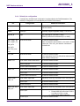
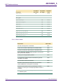
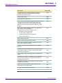
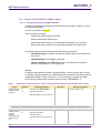
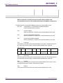
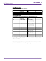
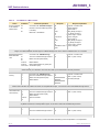
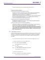
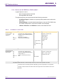
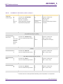
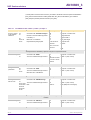
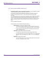
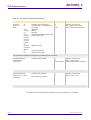
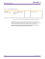
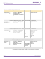
2.4.4 Default pin configuration
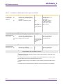
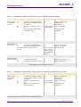
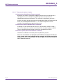
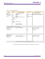
Consequently, the default pin configuration is as described in the PN532 datasheet. (The
default pin configuration is not changed by the PN532C106 firmware).
Pin
I0
Configuration
Additional information
Input
Connect directly to DVDD or to GND (no need of
external resistor)
PVDD
Power pin
Externally supplied regulated voltage, 1.6V to 3.6V
RSTPD_N
Input
NFC reset signal. (Low state = reset)
I1
RSTPD_N must never exceed min(3.6 V, VBAT)
P30 / UART_RX
Quasi bi directional
No need of external resistor.
When connected to the P5CN072, to be used in Virtual
Card mode, P34 / SIC_CLK shall be connected to
P5CN072 I02
P31 / UART_TX
P32_INT0
P33_INT1
P34 / SIC_CLK
P35
P70_IRQ
Quasi bi directional
No need of external resistor.
In the Application Note P70_IRQ will be written as IRQ
when used as interrupt line.
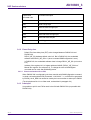
MISO / P71
In I2C mode: Quasi bi directional
No need of external resistor.
In SPI: Push pull
No need of external resistor
In HSU: Quasi bi directional
No need of external resistor
In I2C mode: Quasi bi directional
No need of external resistor.
In SPI: Input
No need of external resistor.
In HSU: Quasi bi directional
No need of external resistor
In I2C mode: Open drain
Use pull up, 1k/V. E.g. for PVDD = 3.3V, 3.3 k pull-up.
In SPI: Input
No need of external resistor
In HSU: Push pull
No need of external resistor
In I2C mode: Open drain
Use pull up, 1k/V. E.g. for PVDD = 3.3V, 3.3 k pull-up.
In SPI: Input
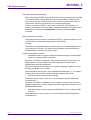
Use resistor bridge or LDO and pull up to be able
• to keep NSS high even when PVDD =
0 (to stay in LowVBAT mode)
• to force a low state to wake up.
In HSU: Input
No need of external resistor
SCK / P72
MOSI / SDA /
HSU_TX
NSS / P50_SCL /
HSU_RX
<DOC_ID>
Application note
© NXP B.V. 2006. All rights reserved.
Rev. 1.2 — 1/14/2010
21 of 75