1
US006076183A
United States Patent
[19]
[11]
Espie et al.
[54]
[451
Patent Number:
Date of Patent:
6,076,183
Jun. 13, 2000
Primary Examiner—Stephen M. Baker
METHOD OF MEMORY ERROR
CORRECTION BY SCRUBBING
Attorney, Agent, or Firm—EdWard J. Kondracki; Miles &
Stockbridge RC.
[75] Inventors: Eric Espie, Villard de Lans; Zoltan
Menyhart, Meylan, both of France
[57]
ABSTRACT
Appl. No.: 08/993,109
The invention relates to a method of correction of corrupted
data stored in a memory location by scrubbing. The memory
is associated With an error correcting code device Which
Filed:
method comprises three steps. During a ?rst step, the data is
Assignee: Bull, S.A., Louveciennes, France
corrects the data transmitted to a user requesting them. The
Dec. 18, 1997
Int. Cl.7 ........................... .. G06F 11/10; G11C 29/00
read from the memory at an address contained in a ?rst
US. Cl. .............................. .. 714/764; 714/6; 714/773
Field of Search ................................... .. 714/764, 754,
reservation is created. During a second step, if a reservation
register, corrected, and stored into a second register. A
exists the data contained in the second register is Written
714/773, 6
back into the same memory location. The reservation is
cleared and a particular ?eld of a condition register is
modi?ed. If a reservation does not exist, the second step is
References Cited
U.S. PATENT DOCUMENTS
5,263,032
5,267,242
5,428,761
11/1993
11/1993
6/1995 Herlihy et al.
third step, the status of the condition register is checked. If
the test is positive the process is ended, the scrubbing being
..... .. 395/425
5,502,728 3/1996 Smith, III
5,588,112 12/1996 Dearth et a1.
5,629,950
5,768,560
completed Without altering the memory location. During the
Porter et a1. ......................... .. 371/40.2
Lavallee et a1. ..
.. 371/10.1
.. 395/18203
.. 395/182.07
successful; if not, an iteration of the three above steps is
executed.
5/1997 Godiwala et a1.
.... .. 371/51.1
6/1998 Lieberman et a1. .................. .. 395/494
23 Claims, 4 Drawing Sheets
SCRUBBING FLOWCHART
@
Loop iterated
FETEHING DATA FROM
MEN 0RY( address Rx)
.XIOO
CORRECTING DATA
(ECC)
_,1Q1
STEP I
LOADING CORRELTED
DATA INTO Ryl register)
CREATING A RESERVATION
STORING comm
0F Ry mm N2 1
MEMORYladdressRx
0
STEP II
202
MARKING A
N203
CONDFHON REGISTER
“STORlNG 0K"
Yes
Scrubbling
completed
STORING DAT
0K” ?
300
N0
STEP III
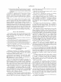
U.S. Patent
Jun. 13,2000
Sheet 1 of4
6,076,183
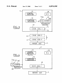
FIGJ PRIOR ART
MEMORY
x-kxx
UNIT
I
ECC
bits
CIRCUlTS
USER —>
XXXX
ECC
bits
If
F|G_2 PRIOR ART
X
X
X
X
ECC
DMA
I
MEMORY
ECC
XXXX
{1 ECC
ECC
bits
XXXX
l
1
EEC
CIRCUITS
bits
l
l
l
|
\
l
l
.1
USER->
XXXX
ECC
bits
fr
2F
fr
)1
D
t2
Time
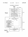
U.S. Patent
Jun. 13,2000
3
Sheet 2 of4
6,076,183
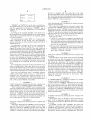
?ENERfAalj
[30
REGISTERS
ALU
Flag
33
(31’
/ (330
cownmow
,3
REGISTERS
331
ADDRESS
RESERVATlON
32
"_
REGlSTER
K
_/Po
CACHE LEVEL 1
5
A
\['n
1+O_/‘l —____r--———__J
C A CHE LEVELZ ‘I,}
r. ___.._____1_______l
4
m/L __..____r______
CACHE LEVEL3 _]l
v
MEMORY UNIT
I
3
MS
I
GENERAL
REGISTERS
ALU
(RX,R)I)
(34
H
39 33 330'
common:
REGISTERS
( / f
32
ADDRESS
\ RESERVATION
§
CACHE EEVEH
331, REGISTER
Y
MEMORY UNIT
”5
U.S. Patent
Jun. 13,2000
Sheet 3 of4
6,076,183
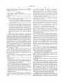
SCRUBBING FLOWCHART
@
Loop i’rera'red
FETCHING DATA FROM
MEMORYI address Rx)
M100
II
CORRECTING OATA
(ECCI
,101
LOADING CORRECTED
’\/102
FlG-S
‘F
ISTEPI
DATA INTO Ry(regisIerI
i
CREATING A RESERVA‘I'IONh/IOB
RESERVATION?
I
200
STORING CONTENT
OF Ry INTO N201
IsTEPn
MEMORYIaddressRxI
I
CLEARING
RESERl/ATION
MARKING A
CONDITION REGISTER
202
N203
“STORING OK"
Yes
SCrubblIng
comple’red
‘
END
/\Q)
sTORING DAT
OK” ?
N0
FSTEPIII
/
6,076,183
1
2
METHOD OF MEMORY ERROR
CORRECTION BY SCRUBBING
Other approaches consist in freeZing or stopping the other
active components in the machine by softWare means While
the data in the corrupted memory is being refreshed.
BACKGROUND OF THE INVENTION
1. Field of the Invention
The above solutions are unsatisfactory.
On the one hand, using additional hardWare devices does
not meet the main requirements of modern computers, i.e.:
The invention relates to a method of memory error
correction by scrubbing.
simpli?cation of the hardWare circuits;
2. Description of the Prior Art
A computer memory is usually equipped With hardware
circuits Which detect errors and repair them. To this end,
Error Correction Code, here-after called “ECC”, is used. The
data in the computer memory contains information bits and
redundant bits computed from the information bits. Such a
drastic reduction of sale costs.
On the other hand, freeZing or stopping the other active
components in the machine by softWare means requires
de?ning “consistency points” Where it can be ensured that
the active components have not got more recent data in their
caches than the memory has (i.e. they have not got any
possibility to Write into the memory, because cache copy
code is capable of supplying correct (i.e. recovered) data to
a particular processing element even if some bits of the data
in the memory are corrupted. This mechanism provides a
15
back or the direct memory access is not under control of the
softWare). This approach can be only used for monoproces
security reserve against the data loss.
The capability to correct corrupted data is primarily
limited by the length of the redundant part of the data.
processor synchroniZation Would be required.
Accordingly, once a data element contains some corrupted
consuming and thus impair the performance of the machine.
Taking advantage of the ECC, a main object of the
sor machines. For multiprocessor machines, too much inter
Furthermore freeZing or stopping mechanisms are time
bits, there is not enough security reserve against additional
bit corruption. Measures have to be taken to reWrite the
corrupted data into the memory With a fresh and corrected
copy. This later task is referred to as memory scrubbing.
BRIEF DESCRIPTION OF THE DRAWINGS
25
FIG. 1, appended to the description, illustrates the above
recalled process. It is assumed that a Word W1 is stored in a
given memory address. In addition to the information bits,
SUMMARY OF THE INVENTION
The invention consists of a method for correcting cor
rupted data stored in a main memory location of a given
ECC bits are provided in order to perform a correction if
needed. It is further assumed that Word W1 contains a
corrupted bit shoWn as an asterisk. When W1 is fetched from
the memory and transmitted to another location of the
computer, called “User”, the ECC circuits 1, using the ECC
bits, repair corrupted Word W1. The transmitted Word, i.e.
W‘l, is thus correct. This operation takes place at time to.
The Word stored in the memory, W1, remains unchanged,
i.e. corrupted. As above recalled, the reserve of security is
address by scrubbing the main memory location, said main
memory being associated With an error correcting code
device in order to correct said corrupted data as they are read
35 from said main memory location and transmitted to a user
requesting such data, reading and Writing of data from and
into said main memory being under control of a processor,
the method consisting in an iterative loop comprising the
loW, and the data may be further corrupted, even to an extent
three folloWing steps:
that it cannot be corrected (due to the limited correction
capacity of the ECC bits). To avoid this adverse effect, it is
necessary to refresh the memory With corrected data, i.e.
Word W‘l. At time t1, this data is Written back into the same
memory or address. The ECC bits recover their full correct
ing capacity.
The basic problem is that any active components
45
a second step comprising a stage of checking Whether a
reservation information associated to said given
may modify at any moment the data to be refreshed, and
consequently, a race condition can develop: if an active
address exists, and:
(i) if the condition checked is true, executing the
folloWing further stages: storing the content of said
component modi?es the data before the refreshment can take
by ECC circuits 1 and transmitted to a “User”.
At time t1, a neW Word W2 is Written into the same
memory location through a DMA circuit 2 and modi?es the
content of that memory location. HoWever, at time t2, the
corrected Word W‘1 is Written back into that memory loca
tion (as at time t1 in FIG. 1). Word W2 is thus lost.
To overcome this problem, the existing prior art solutions
use techniques to exclude the active components from
accessing the memory.
Some existing machines achieve data refreshment by
means of additional hardWare devices making memory
reading and correction cycles indivisible.
a ?rst step comprising a stage of fetching data from said
main memory location of given address, a stage of
correcting said data by means of said error correcting
device, a stage of loading said corrected data into a
second memory location, and a stage of creating a
reservation information associated to said given
address;
(processors, DMA-s, i.e. Direct Memory Access devices),
place, the neW data is going to be lost, because the scrubbing
mechanism Writes back the original data.
FIG. 2, appended to the description, illustrates the above
recalled process. As in FIG. 1, Word W1 is corrupted. At time
to, Word W1 is read from a given memory location, corrected
invention is to offer the possibility to refresh the corrupted
data Without any additional hardWare support or disturbing
the operations of the other active components, such as
processors, DMA-s, etc.
The invention is directed to alleviating the draWbacks of
the prior art devices, some of Which have just been referred
to, and to meeting the stated requirements.
second memory location into said memory location
of given address, in order to perform said scrubbing,
erasing said reservation information, storing a pre
55
determined condition information into a third
memory location, in order to re?ect the effective data
storing into said main memory location of given
address, and
(ii) if the condition checked is false, executing a stage
consisting in completing said second step Without
altering the content of said main memory location of
said given address;
and a third step comprising a stage of checking the status
of said condition information, and:
(i) if said status indicates that said storing corrected
data has failed, executing an iteration of the above
three steps,
6,076,183
4
3
(ii) if said status indicates that said storing of corrected
assumed that processor 3 is directly attached to memory unit
data has been executed, ending said loop, scrubbing
5, via a bus (dotted line).
of said main memory location of given address being
When data are read from main memory unit 5, a copy is
Written into cache memory 32.
successful.
According to a preferred embodiment of the invention,
the process is implemented in a “PoWerPCTM” based
machine. A processor of the latter type (for example a
processor such as “PoWerPCTM604”) provides a data pro
The process of refreshing the memory by scrubbing
tection called “reservation”, Which Will be later explained in
detail.
Contrary to the existing solutions Which exclude all other
memory accesses While the memory scrubbing is taking
place, the approach according to the invention can start the
memory scrubbing at any moment, Without any need of
10
more particularly associated to a so-called reservation
mechanism. Here-after, “instruction LWARX” and “instruc
tion STWCX.” Will be replaced by “LWARX” and
“STWCX”
synchroniZation or mutual exclusion. It makes use of an 15
instructions sequence that fails and restarts if somebody is
modifying the same data area. If this scrubbing instruction
mentioned “User’s Manual”.
This instruction creates a reservation for use by a store
Any operating system can take advantage of this mecha
Word conditional instruction. This operation consists in
storing an address associated With the reservation into the
?rst ?eld 330 of the register 33, and in setting the ?ag stored
msm.
LIST OF THE DRAWINGS
in the second ?eld 331 to a value re?ecting that a reservation
25
features and advantages Will emerge from reading the fol
FIGS. 1 and 2 illustrate methods according to the prior art
and draWbacks thereof;
ervation (?eld 330 of register 33) and replaces any address
FIG. 3 illustrates a machine implementing the method of
the invention according to a preferred embodiment;
35
scrubbing according to the invention.
As above, the target address EA is the sum (rA|( ))+(rB).
If a reservation exists (?ag stored in ?eld 331 of register 33),
DETAILED DESCRIPTION OF THE
INVENTION
the contents of the register rS are stored into the Word in
memory location addressed by EA and the reservation is
cleared (bits of ?eld 331 set to Zero). If no reservation exists,
Though the invention is not limited to “PoWerPCTM”
based machines, the folloWing detailed description applies
the instruction completes Without altering said memory
45
is set to re?ect Whether the store operation Was performed,
i.e. Whether a reservation existed When the “STWCX.”
RISC Microprocessor User’s Manual”, both published by
began execution. A bit in the condition ?eld CR( ), called
MOTOROLA Inc., in 1993 and 1994 rsp.
FIG. 3 is a block diagram shoWing the main parts of a
processor 3 according to the preferred embodiment. In
“EQ” (namely bit No. 2), is set to “1” if the data store Was
completed successfully.
The invention takes advantage of this mechanism (or
typical manner, processor 3 comprises an ALU (Arithmetic
more generally of a similar mechanism as it Will be
described With respect to FIG. 5), as Well as the existence of
Logic Unit) 30, general registers 31, condition registers 34,
and a built-in ?rst level cache memory 32, plus other
a ?rst ?eld 330 dedicated to the storing of a Word specifying
a memory location to be scrubbed, and a second ?eld 331
dedicated to the storing of a ?ag. The mechanism of the
reservation Will be explained hereafter.
Processor 3 communicates With a memory unit 5, directly
location.
A condition register ?eld, called “CR( ) Field”, is used. It
Such processors are described in “PoWerPCTM 601—RISC
Microprocessor User’s Manual” and “PoWerPCTM604—
Well-knoWn circuits (clock circuits, etc.) not shoWn. Cache
memory 32 is split into lines IO to In of a given byte-length.
More speci?cally, it contains a register 33, so-called
“reservation register”. The register 33 is split into tWo ?elds:
previously associated With the reservation.
The complete name of the second instruction, i.e.
“STWCX.”, is “Store Word Conditional Indexed”. This
instruction is associated With three registers called rS, rA and
rB. A detailed description of this instruction is also given in
the above-mentioned “User’s Manual”.
FIG. 6 is a multiprocessor according to the invention.
to such a con?guration (Which constitutes the preferred
embodiment), unless otherWise stated.
is created (for example setting a bit to “1”). Atarget address
called EA, is computed from tWo other address Words
contained in tWo general registers called rA and rB. More
precisely EA is the sum (rA|( ))+(rB). The Word in memory
addressed by EA is loaded into a further register called rD.
An address computed from EA is associated With the res
loWing description, given With reference to the appended
draWings Wherein:
FIG. 4 illustrates a machine implementing the method of
the invention according to a more general embodiment;
FIG. 5 is a ?oWchart of the error correcting method by
The complete name of the ?rst instruction, i.e. “LWARX”,
is “Load Word and Reserve Indexed”. This instruction is
associated With three registers called rD, rA and rB. A
detailed description of this instruction is given in the above
sequence reaches its end, then it is sure that no other active
component has modi?ed the same memory location in the
meantime and therefore the race condition Was avoided.
The invention Will be more clearly understood and other
according to the invention Will be noW explained.
The standard instructions set of the “PoWerPCTM” pro
cessors comprises, among others, the tWo folloWing ones
called “LWARX” and “STWCX.” instructions, Which are
55
ECC, to implement a refresh process using scrubbing Which
alloWs memory accesses While the memory scrubbing is
taking place, the memory scrubbing starting at any moment,
Without any need of synchroniZation or mutual exclusion.
The invention makes use of an instructions sequence that
fails and restarts if somebody is modifying the same data
area. If the scrubbing instruction sequence reaches its end,
then it is sure that no other active component has modi?ed
the same memory location in the meantime, therefore the
or through one or more optional caches 4, called second 65 race condition Was avoided.
level cache 40, and in some cases a third level cache 41, as
The particular scrubbing sequence is the folloWing itera
shoWn in FIG. 3. For the sake of simplicity, it Will be
tive sequence of instructions:
6,076,183
6
LWARX
Ry, O, Rx
STWCX.
Ry, O, Rx
BNE
loop
the error is repaired. The data cache line of the other
processor gets killed. There is no iteration (loop). The cache
line of the other processor containing the data may have to
be re-fetched if the load instruction has not been completed
before “STWCX.” obtains exclusivity.
EXAMPLE 3
“Data load-modify-store” instruction by another processor
competes With scrubbing.
“LWARX” and “STWCX.” are the above recalled stan
The cache line containing the data gets loaded. This
dard instructions. Ry, 0, and Rx refer to the registers rD, rA
and rB, respectively, for instruction “LWARX”, and to
operation and “LWARX” can be executed in any order. The
loaded data is correct. “LWARX” gets the correct data and
obtains the reservation. The states of both caches are shared.
registers rS, rA and rB, respectively, for instruction
“STWCX.”.
According to the example described, rA is alWays Zero.
More speci?cally, it is assumed that Rx is one of the general
register 31 and contains the address to be scrubbed, and Ry
15
There are tWo cases:
is a scratch register.
The loop instruction called “BNE” is a “branch condi
tional” instruction. In the present case, this instruction
If “STWCX.” Wins, then it completes successfully, the
error is repaired. There is no iteration (loop). The cache
line of the other processor containing the data has to be
re-fetched for the sake of the pending store. Finally, the
store Will be accomplished.
If the store of the other processor Wins, then the error gets
checks a particular bit of the condition register ?eld CR( ),
namely bit No. 2.
To summarise, during the ?rst step (instruction
“LWARX”) data load takes place and a reservation in
register 33 is made. Due to the ECC, the data loaded are
25
correct. During the second step (instruction “STWCX.”), if
EXAMPLE 4
“Data store” instruction by another processor competes With
scrubbing.
to Zero at the beginning of instruction “STWCX”. During
the third step, the instruction “BNE” checks this bit. If the
store operation Was not completed during the previous step
(i.e. scrubbing is not achieved), the loop is iterated once
35
It is enough that a processor has the corrected data in its
If the data line is in the cache of the processor intending
to execute the store, then this situation is covered by the
previous case 3. Otherwise, “LWARX” gets the correct data
and obtains the reservation. The processor intending to
execute the store issues a read With intention to modify type
bus cycle that kills the data obtained by “LWARX” (the
reservation gets lost too) and fetches the cache line (the data
cache in modi?ed state. Since then, there can be no more
access to the defective data in the memory. A corrected data
is correct). It inserts the data of the store into the cache line.
The data in memory location to be scrubbed Will be correct
is provided to anyone Who Wants to access it. Eventually the
corrected data Will replace the corrupted one in the memory.
NoW, the main situations When a scrubbing sequence
collides With another memory cycle, ie when there is
contention for accessing the memory location to be
scrubbed, Will be detailed beloW. Obviously, if there is no
other access to said memory location, the scrubbing opera
tion can be executed Without any problem.
repaired. The scrubbing loop Will do another iteration.
“LWARX” forces the copy-back operation to take
place. Next “STWCX.” succeeds.
a reservation exists (?ag stored in ?eld 331 of register 33),
the content of Ry is stored into the Word addressed by Rx.
If the store is completed, bit “EQ” of the Condition register
“CR( )” is set to “1”. Obviously, said bit “EQ” must be reset
again.
“STWCX.” and the store competes for obtaining exclusivity.
The data cache line of the looser processor gets killed, if
“STWCX.” has lost, the reservation gets lost, too.
When the copy-back takes place. “STWCX.” fails. The
scrubbing loop Will do another iteration and next “LWARX”
forces the copy-back operation to take place. Next
“STWCX.” succeeds.
EXAMPLE 5
45
A “LWARX/STWCX.” instructions sequence by another
processor competes With scrubbing.
Both of the tWo “LWARX” instructions get the correct
data. One of the tWo “STWCX.” instructions succeeds (the
data is corrected), the other loop has to repeat its iteration.
EXAMPLE 1
“fetch” instruction by another processor (eg a processor in
another machine or module) competes With scrubbing.
“LWARX” forces the copy-back operation to take place. The
“Fetch” instruction and “LWARX” can be executed in any
order. The caches tolerate if the same line is accessed as data
correctness of competing “LWARXISTWCX.” instructions
sequences is the very essence of the multiprocessor archi
and instruction. Due to the ECC, the instruction fetched is
tecture synchroniZation.
correct. There Will be no Write-back due to this “Fetch”
instruction. “LWARX” gets the correct data and obtains the
reservation. “STWCX.” obtains the exclusivity (the instruc
tion cache is not affected) and completes successfully; the
error is thus repaired. There is no iteration (loop).
55
EXAMPLE 6
A “DCBZ” instruction by another processor competes With
scrubbing.
“Data load” instruction by another processor competes With
The complete name of “DCBZ” is “Data Cache Block to
Zero”. It is an instruction specially dedicated to certain
cache memory operation. It alloWs to clear to Zero all bytes
scrubbing.
of a block.
EXAMPLE 2
If “DCBZ” executes after “LWARX” but before the
“Data load” instruction and “LWARX” can be executed in
any order. Due to the ECC, the data loaded is correct. There
“STWCX.” instruction, then it kills the data obtained by
Will be no Write-back. “LWARX” gets the correct data and 65 “LWARX” (the reservation is lost too). The processor hav
ing executed “DCBZ” oWns the cache line corresponding to
obtains the reservation. The states of both caches are shared.
the defective memory location in modi?ed state. The scrub
“STWCX.” obtains exclusivity and completes successfully,
6,076,183
8
7
As already indicated, according to the preferred
bing loop Will do another iteration and next “LWARX”
forces the copy-back operation to take place and subsequent
embodiment, the machines are based on a “PoWerPcTM”
“STWCX.” succeeds.
microprocessor. Though it is very ef?cient to use such a
processor because the so-called “reservation mechanism”
and the instructions as Well as the hardWare (reservation
EXAMPLE 7
“DMA accesses” compete With scrubbing.
Any “DMA” sequence falls into already described
register) needed to implement said mechanism are provided
as standard, it should be clear hoWever that the invention is
not limited to this sole architecture.
examples 2, 4 or 6.
The above recalled examples may be summarized as
folloWs:
a/ If the scrubbing loop has completed successfully, then
Generally speaking, in order to implement the iterative
10
requirements have to be met.
the error has been repaired, because:
it is sure that nobody else Wanted to modify the data;
With respect to the hardWare, the microprocessor (see
FIG. 3: 3) must comprise general registers and condition
the content of the memory location to be scrubbed has
not been altered (With respect to the data supplied by
the ECC logic).
scrubbing loop according to the invention, the folloWing
registers. These registers are needed to store the address to
15
be scrubbed (register Rx), the content of this address
b/ If someone else is modifying the content of the memory
(register Ry), after the correcting process (ECC) is
location to be scrubbed, then the scrubbing loop fails.
performed, and a condition register (FIG. 3: 34). Such
registers do exist in any integrated microprocessors.
As explained in the examples, if an other process
“Wins”, i.e. it Writes neW data into said memory loca
According to an essential feature of the invention, a
tion before the scrubbing process completes (see for
example FIG. 2). The reservation is lost (bits of ?ag
stored in ?eld 331 of register 33 cleared). The scrub
bing process according to the invention does not
modify the data in any Way and retries the operation
later.
For most of the memory operations, it is very important
to achieve What is called a “coherency”, specially With
respect to the “DMA” operations, and more especially in a
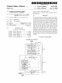
multiprocessor architecture, as shoWn in exemplary form in
FIG. 6. FIG. 6 shoWs multiprocessor 50 including a plurality
further register is needed, i.e. the so-called “reservation
register”. If the microprocessor does contain any built-in
register Which can be employed to this end, an external
memory location constitutes an alternative solution, eg an
external dedicated register.
25
FIG. 4 is a block diagram shoWing the architecture of this
further embodiment. As in the preferred embodiment (FIG.
3), processor 3‘ comprises an ALU 30, general registers 31,
conditions registers 34 and a cache memory 32. Processor 3‘
communicates With a main memory unit 5 through a bus
of processors (P) indicated by reference numerals 3, 3‘, 3“,
(dotted line). HoWever, contrary to the processor 3 (FIG. 3),
each having an architecture such as, for example, processor
3, illustrated in FIG. 3. Each of processors 3, 3‘, 3“ has
a built-in “reservation register” is not provided. An external
register 33‘ acts as a “reservation register”. It is also split into
respective cache C, C‘, C“, Which are comparable to cache
32 shoWn in FIG. 3. Multiprocessor 50 includes appropriate
bus 52 connecting processors 3, 3‘, 3“ With other multipro
cessor 50 components, including I/O 54, ALU 56, and
memory (M) 58, all cooperating in knoWn manner. Memory
tWo ?elds: a ?rst ?eld 330‘ intended to store an address
associated to the reservation, and a second ?eld 331‘
35 intended to store a ?ag. This ?ag can be one sole bit and is
set to a predetermined value re?ecting Whether a reservation
(58) further includes a means for running a coherency
FIG. 5 is a ?oWchart implementing a scrubbing iterative
loop according to the invention. This ?oWchart shoWs a
exists or not.
protocol function (CP) 60.
An example of coherency protocol is given by the
three-step iterative process of memory scrubbing Which
meets the speci?c features of the invention, i.e. Without any
need for synchroniZation or mutual exclusion.
STEP I comprises four stages: 100 to 103.
Stage 100 consists in data fetching from memory 5 at the
so-called “MESI” protocol, Which is described in the pre
viously cited “User’s Manuals”. Bus snooping is used to
drive a four-state cache coherency protocol Which ensures
the coherency of all processor and direct-memory access
(DMA) transactions.
45
granularity, typically at a granularity of 32-byte cache
memory location to be scrubbed.
Stage 101 consists in data correction by means of ECC
blocks.
circuits (not shoWn).
The four possible states for a block in a cache are the
folloWing ones:
1. Modi?ed: The addressed block is valid in the cache and
in only this cache. The block is modi?ed With respect to
the system memory. The modi?ed data in the block has
not been Written back to the memory.
2. Exclusive: The addressed block is in this cache only. The
data in this block is consistent With system memory.
3. Shared: The addressed block is valid in the cache and in
at least one other cache. This block is alWays consistent
With system memory. The shared state is shared
address contained in register Rx (or computed from the
content of this register). Said address is relating to the
The coherency of memory is maintained at a certain
Stage 102 consists in loading of so corrected data into
register Ry.
55
Stage 103 consists in creating a reservation. This opera
tion consists in storing an address associated With the
reservation into the ?rst ?eld 330‘ of the register 33‘, and in
setting the ?ag stored in the second ?eld 331‘ to a value
re?ecting that a reservation is created (for example setting a
bit to “1”). The reservation address stored in the ?rst ?eld
330‘ is computed from the content of register Rx. The
manner in Which the address to be associated With the
reservation is computed depends on the speci?c architecture
unmodi?ed. There is no shared-modi?ed state.
4. Invalid: This state indicates that the addressed block is not
resident in the cache and/or any data contained is not
considered useful.
of the machine. It is the result of an effective address
calculation Well knoWn in the art. This address replaces any
exclusive access to an addressed block before an update is
address previously associated With the reservation.
STEP II also comprises four stages: 200 to 203.
Stage 200 consists in a checking operation. The content of
register 33‘ is checked, in particular the status of the ?ag in
made.
the second ?eld 331‘. If a reservation exists for the address
Coherency is a very important feature of multiprocessor
systems. For example, a given processor must obtain an
65
6,076,183
10
to be scrubbed (branch “Yes”), stages 201 to 203 are
microprocessor in question (i.e. instructions performing
executed. On the contrary (branch “No”), the process is
STEP I or STEP II, rsp., at one go), it is alWays possible to
divide each step into a sequence of substeps (or stages as
shoWn in FIG. 5). For example, stage 200 consists in a
directed to STEP III. In other Words, no storing operation is
performed and the process completes Without altering the
memory location to be scrubbed.
“conditional branch” instruction Which is very common.
It means that “someone else” (i.e. another process) has
modifyied the content of the location to be scrubbed, then
“BNE” Which forces the iteration (loop) is also a “condi
tional branch” instruction.
While the preferred forms and embodiments of the inven
tion have been illustrated and described, it Will be apparent
to those of ordinary skill in the art that various changes and
modi?cations may be Without deviating from the inventive
concept and spirit of the invention as set forth above, and it
is intended by the appended claims to de?ne all such
concepts Which come Within the full scope and true spirit of
the invention.
What is claimed is:
1. Amethod for correcting corrupted data stored in a main
the scrubbing loop fails. As explained in the examples, if
another process “Wins”, ie it Writes neW data into the
memory address to be scrubbed before the scrubbing process
10
completes (see for example FIG. 2). The reservation is lost
(bits of ?ag stored in ?eld 331‘ of register 33‘ cleared).
Stage 201 consists in storing the content of register Ry
into the memory location addressed by Rx (or an address
computed from this address Word), ie the memory location
15
to be scrubbed.
Stage 202 consists in clearing the reservation. In
particular, the ?ag in ?eld 331‘ is altered to re?ect that there
is no more reservation (for example, the above-mentioned
bit is set to “0”).
Stage 203 consists in modifying a speci?ed ?eld of a
memory location of a given address by scrubbing of the
main memory location, said main memory being associated
With an error correcting code device in order to correct said
corrupted data as the data is read from said main memory
location and transmitted to a user requesting such data,
given condition registers 34, for example in setting a pre
determined bit to the value “1”. This operation re?ects a
status Which may be called “storing OK”.
Obviously, said bit must be reset to “0” at the beginning
of STEP II.
Wherein reading and Writing data from and into said main
memory is under control of a processor, the method com
25
STEP III comprises only one stage: 300.
After that STEP 11 is completed, Whatever the path
corrected data into a second memory location, and
creating a reservation information associated to said
folloWed (branch “Yes” or branch “No”), a neW check is
performed. Stage 300 consists in checking the status of the
condition register storing said speci?ed ?eld to determine
Whether the storing Was completed during STEP II (stage
given address;
(b) a second step comprising checking Whether the res
ervation information associated With said given address
201) or not.
If the condition “storing data OK” is true (branch “Yes”),
the process is ended and the scrubbing loop has completed
successfully. Then the error has been safely repaired. It is
prising the three folloWing steps in an iterative loop:
(a) ?rst step comprising fetching data from said main
memory location of given address, correcting said data
by means of said error correcting device, loading said
35
exists, and:
(i) if the condition checked is true, executing the
folloWing further steps:
storing the corrected data in said second memory
location into said memory location of given
address in order to perform said scrubbing of the
main memory location, erasing said reservation
sure that no other process (DMA and so on) Wanted to
modify the data stored in the scrubbing memory location.
If the condition “storing data OK” is false (branch “No”),
the scrubbing sequence has failed and STEPI to STEP III are
iterated (loop) again. The data in memory location to be
information, storing a predetermined condition
scrubbed are not modi?ed in any Way.
information into a third memory location in order
to re?ect the effective content of said second
With respect to the branch “No” of step II, it is important
memory location storing into said main memory
to note that, as stage 203 is not executed, the check per
formed at stage 300 alWays fails.
45
It is also important to note that each of the above detailed
STEP I to STEP III must be considered as a unitary
location of given address, and
(ii) if the condition checked is false, executing a step
consisting of completing said second step Without
operations set. In other Words, all the operations (called
altering the content of said main memory location of
stages in the ?oWchart) are under control of processor 3‘.
The latter must ascertain that a particular step (STEPI to III)
is completed before executing the folloWing one. It must
also ascertain the correctness of the various operations and
maintain the coherency betWeen the various cache
said given address;
memories, ie a predetermined coherency protocol is
adhered to.
A reading of the above description con?rms that the
invention achieves the stated objectives.
It should be clear, hoWever, that invention is not limited
to the embodiments previously described, in particular With
55
(c) and a third step comprising checking the status of said
condition information, and:
(i) if said status indicates that said storing corrected
data has failed, executing an iteration of the above
three steps, and
(ii) if said status indicates that said storing of corrected
data has been executed, ending said loop, Whereby
said indication means that scrubbing of said main
memory location of given address is successful.
2. Amethod according to claim 1, Wherein said processor
memory location dedicated to the reservation data is pro
is an integrated microprocessor comprising a plurality of
general registers, and said given address to be scrubbed is
stored in a ?rst general register.
3. A method according to claim 2,Wherein said second
vided (for example an external register), any existing inte
memory location is a second general registrer Which stores
reference to FIGS. 3 to 5. As a matter of fact, as already
stated, the invention is not limited to a machine based on
speci?c integrated microprocessors. On condition that a
grated microprocessor or even discrete processor can be 65 the said corrected data.
used. If instructions “LWARX” and “STWCX.” or similar
4. Amethod according to claim 1, Wherein said processor
are not provided in the standard instructions set of the
is an integrated microprocessor and further comprising at
6,076,183
11
12
least one condition register, said condition information being
stored in a predetermined ?eld of said condition register.
5. A method according to claim 4, Wherein said condition
means responsive to said determining means for
preventing, When said reservation information is not
present, said corrected data from being stored in said
main memory location;
information consists in one sole bit Which is set to the logic
value “1” When said data storing is executed.
6. Amethod according to claim 1, Wherein said processor
means for checking a status of said predetermined con
dition information;
is associated With a dedicated register divided into a ?rst and
means responsive to said status checking means, When
a second ?eld, and Wherein said stage of creating reservation
information consists in storing into said ?rst ?eld an address
Word specifying said given address to be scrubbed, and
storing into said second ?eld a ?ag re?ecting Whether a
reservation exists or not for said given address.
7. Amethod according to claim 6, Wherein said processor
is an integrated microprocessor and said dedicated register is
a built-in register.
8. Amethod according to claim 6, Wherein said processor
is an integrated microprocessor and said dedicated register is
an eXternal register.
9. A method according to claim 6, Wherein said ?ag
said predetermined condition information indicates that
said corrected data has not been stored in said main
10
corrected data storing means to store corrected data in
said main memory location; and
means responsive to said status checking means, When
15
said predetermined condition information indicates that
said corrected data has been stored in said main
memory location, for ceasing operation of said appa
ratus With respect to said data fetched from said main
memory and With respect to said corrected data.
16. Apparatus as recited claim 15, Wherein said processor
consists in one sole bit Which is set to the logic value “1”
When said reservation eXists.
10. A method according to claim 1, Wherein said proces
sor is an integrated microprocessor comprising a built-in
cache memory and said corrected data read from said
is an integrated microprocessor comprising a plurality of
general registers, and Wherein an address for said main
memory location from Which data is fetched is stored in a
?rst general register.
memory being copied in predetermined locations of said
cache memory.
memory location, for initiating further attempts by said
17. Apparatus as recited in claim 16, Wherein said second
25
11. A method according to claim 10, Wherein said prede
termined locations contain blocks of a predetermined byte
memory location comprises a second general register.
18. Apparatus according to claim 15, Wherein said pro
12. A method according to claim 10, Wherein the com
pleteness and the correctness of each of said three steps are
under control of said processor.
13. A method according to claim 10 Wherein said proces
cessor is an integrated microprocessor and Wherein said
third memory location comprises at least one condition
register, and Wherein said condition information is stored in
a predetermined ?eld of said condition register.
19. Apparatus as recited in claim 15, Wherein said pro
sor is a part of a multiprocessor machine comprising a
cessor is associated With a dedicated register divided into a
length.
plurality of cache memories Where data are copied, the
method further comprises a predetermined coherency pro
tocol under control of said processor ensuring the coherency
betWeen said plurality of cache memories.
?rst ?eld and a second ?eld, and wherein said means for
generating reservation information stores, in said ?rst ?eld,
35
14. A method according to claim 11 Wherein said proces
sor is a part of a multiprocessor machine comprising a
plurality of cache memories Where data are copied, the
method further comprises a predetermined coherency pro
tocol under control of said processor ensuring the coherency
betWeen said plurality of cache memories.
15. Apparatus for correcting corrupted data stored in a
location in a ?rst main memory, by a memory scrubbing
technique, said main memory being under control of a
45
processor, comprising:
an address Word specifying said address of said main
memory location, and stores, in said second ?eld, a ?ag
indicating the presence of reservation information associ
ated With said address.
20. Apparatus as recited in claim 19, Wherein said pro
cessor comprises an integrated microprocessor, and Wherein
said dedicated register is a built-in register.
21. Apparatus as recited in claim 19, Wherein said pro
cessor comprises an integrated microprocessor and Wherein
said dedicated register is an external register.
22. Apparatus as recited in claim 15, Wherein said pro
cessor comprises an integrated microprocessor having a
means for fetching data from said main memory location;
an error correcting device for correcting said data;
built-in cache memory.
means for loading corrected data into a second memory
location in a ?rst main memory, by a memory scrubbing
technique, said main memory being under control of a
23. Apparatus for correcting corrupted data stored in a
location;
processor, comprising:
means for generating and storing reservation information
associated With an address of said main memory loca
tion;
means for determining the presence of said reservation
information associated With said address of said main
55
means for loading corrected data into a second memory
memory location;
means responsive to said determining means for storing
said corrected data in said main memory location, When
said reservation information is present;
means for erasing said reservation information When said
corrected data is stored;
means for storing a predetermined condition information
in a third memory location, said predetermined condi
tion information being indicative of Whether said cor
rected data has been stored in said main memory
location;
a multiprocessor machine having a plurality of cache
memories Where data are copied;
means for fetching data from said main memory location;
an error correcting device for correcting said data;
location;
means for generating and storing reservation information
associated With an address of said main memory loca
tion;
means for determining the presence of said reservation
information associated With said address of said main
memory location;
65
means responsive to said determining means for storing
said corrected data in said main memory location, When
said reservation information is present;
6,076,183
14
13
means for erasing said reservation information When said
said corrected data has not been stored in said main
corrected data is stored;
memory location, for initiating further attempts by said
corrected data storing means to store said corrected
means for storing a predetermined condition information
in a third memory location, said predetermined condi
tion information being indicative of Whether said cor
rected data has been stored in said main memory
data in said main memory location;
means responsive to said status checking means, When
said predetermined condition information indicates that
said corrected data has been stored in said main
memory location, for ceasing operation of said appa
location;
means responsive to said determining means for
preventing, When said reservation information is not
present, corrected data from being stored in said main
memory location;
means for checking a status of said predetermined con
dition information;
means responsive to said status checking means, When
said predetermined condition information indicates that
10
ratus With respect to said data fetched from said main
memory and With respect to said corrected data, and
means for running a predetermined coherency protocol,
under the control of said processor, to ensure coherency
betWeen said plurality of cache memories.