1
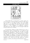
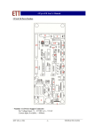
User Manual For ET-ARM BASE2103/2106 ET-ARM BASE2103/2106 ET-ARM BASE2103 which is Board Microcontroller ARM7TDMI-S Core family uses Microcontroller 16/32–Bit 48 Pin low power type to be permanent MCU on board and uses MCU No.LPC2103/2106 from Philips. Board is designed a small size and easy to apply for various project works. MCU is arranged with necessary components as ETT Port 10PIN and uses Power Supply as +5V. Moreover, GPIO can support signal 5V. There is Connector UART0 (RS-232) 2 Ports for Download Hex File and using as RS232 Serial Port Communication for Program Application. Specifications of Board if using LPC2106 16/32-Bit MCU ARM7TDMI-S family No.LPC2106 from Philips Crystal 19.6608 MHz; MCU can collect data maximum high speed 58.9824 MHz if using with Phase-Locked Loop (PLL)internal MCU Support In-System Programming (ISP) and InApplication Programming (IAP) through On-Chip Boot-Loader Software of Port RS232-1 1 Port JTAG 20PIN for Real Time Debugging 1 Port LCD standard ETT 14PIN 4 Port GPIO 10PIN standard ETT 128KB Flash Memory and 64KB RAM +5V Power Supply Maximum 32 I/O Pins GPIO (only GPIO supports signal 5V) Pin GPIO can be used with other functions as following; SPI 1 Channel I2C 1 Channel UART Full-Duplex 2 Channel; RS232-1 and RS232-2 standard 4 Pin ETT Timer 32-bit 1 Channel (7 Input Capture / 7 Output Compare) Watchdog Timer Real Time Clock PWM Output 6 Output ETT CO.,LTD. -1- WWW.ETT.CO.TH User Manual For ET-ARM BASE2103/2106 Specifications of Board if using LPC2103 16/32-Bit MCU ARM7TDMI-S family No.LPC2103 from Philips Crystal 19.6608 MHz; MCU can collect data maximum high speed 58.9824 MHz if using with Phase-Locked Loop (PLL) internal MCU Support In-System Programming (ISP) and InApplication Programming (IAP) through On-Chip Boot-Loader Software of Port RS232-1 1 Port JTAG 20PIN for Real Time Debugging 1 Port LCD standard ETT 14PIN 4 Port GPIO 10PIN standard ETT 32KB Flash Memory and 8KB RAM RTC (Real Time Clock) 32.768KHz with Battery Backup +3V +5V Power Supply maximum 32 I/O Pins GPIO (only GPIO support signal 5V)Pins GPIO can be used with other Functions as following; SPI 2 Channel I2C 2 Channel 8-Channel 10 Bit A/D Converter UART Full-Duplex 2 Channel; RS232-1 and RS232-2 standard 4 Pin ETT Timer 32-bit 2 Channel (7 Input Capture / 7 Output Compare) Timer 16-bit 2 Channel (3 Input Capture / 7 Output Compare) Watchdog Timer, PWM Output ETT CO.,LTD. -2- WWW.ETT.CO.TH User Manual For ET-ARM BASE2103/2106 Structure of Board ET-ARM BASE2103/2106 1 3 2 4 5 6 7 18 17 8 9 10 11 12 16 15 14 13 No. 1 and 3 is Port Communication RS232-2 and RS232-1 respectively. 2 3 4 GND GND 1 TX2 4 RX2 3 +5V 2 TX1 +5V 1 RS232-2 RX1 RS232-1 • No. 2 is Set Jumper as Enable or Disable signal GPIO of P0.8 and P0.9 to be RS232-2 or GPIO. ENA/DIS ENA/DIS Select Jumper For RS232-2 Select Jumper For GPIO ETT CO.,LTD. -3- WWW.ETT.CO.TH User Manual For ET-ARM BASE2103/2106 • No. 4 and 6 is Switch RESET and LOAD respectively. • No. 5 and 7 is LCD Connector 14PIN and VR-10K for contrasting the brightness of LCD Monitor respectively. Circuit and Signal is arranged as following; +5V +VCC RS EN 10K +V RS EN D1 D3 D5 D7 P0.19 P0.17 P0.21 P0.22 1 3 5 7 9 11 13 2 4 6 8 10 12 14 GND VO RW D0 D2 D4 D6 P0.18 P0.20 P0.22 ET-CLCD GND VO RW D1 D3 D5 D0 D2 D4 D7 D6 ET-CLCD • No. 8, 11, 16, and 18 is GPIO0 is divided into 4 Ports and has 8 Bit per Port, totally 32Bit (only GPIO can support Signal 3.3V and 5V). P0.0 P0.1 P0.8 P0.9 P0.2 P0.3 P0.10 P0.11 P0.4 P0.5 P0.12 P0.13 P0.6 P0.7 P0.14 P0.15 +3V3 GND +3V3 GND PORT0[0..7] PORT0[8..15] P0.16 P0.17 P0.24 P0.25 P0.18 P0.19 P0.26 P0.27 P0.20 P0.21 P0.28 P0.29 P0.22 P0.23 P0.30 P0.31 +3V3 GND +3V3 GND PORT0[16..23] PORT0[24..31] Figure displays the Signal GPIO arrangement of all 4 sets. ETT CO.,LTD. -4- WWW.ETT.CO.TH User Manual For ET-ARM BASE2103/2106 • • • • No. 9 is Crystal Oscillator 32.768 KHz for RTC (only version LPC2103). No. 10 is MCU ARM7TDMI-S LPC2103 or LPC2106 from Philips. No.12 is Crystal 19.6608 MHz for MCU . No. 13 is Set Jumper for selecting RUN Mode or Debugging Mode RUN/DEB RUN/DEB Set Jumper as Run Mode Set Jumper as Debug Mode • No. 14 is JTAG Connector 20PIN for Interfacing with JTAG Debugger. Circuit and Signal are arranged as following; +3V3 100K * 5 VTref TRST +VTref TRST TDI TMS TCK RTCK TDO RST# P0.27 P0.30 P0.28 P0.29 RTCK P0.31 RST# 1 3 5 7 9 11 13 15 17 19 +VTarget GND GND GND GND GND GND GND GND GND 2 4 6 8 10 12 14 16 18 20 ARM-JTAG VTarget GND 100K TDI TMS GND GND TCK RTCK GND GND TDO RES# NC GND GND GND NC GND ARM JTAG Pin Connector • No.15 is Connecting Point of Power Supply +5V and GND for supplying only DC+5V into Board. The Connector is arranged as the picture below. +VIN 2 +5V GND 1 • No. 17 is red LED to display status operation of Power Supply. ETT CO.,LTD. -5- WWW.ETT.CO.TH User Manual For ET-ARM BASE2103/2106 To Download Hex File into MCU of Board We use program “LPC2000 Flash Utility V2.3.3” of Philips to Download Hex File into Flash Memory of MCU internal board and we can download this Program free without any charge from www.semiconductors.philips.com. In this case, it communicates with MCU through Serial Port of computer PC. The procedure to Download HEX File into MCU 1. Interface Cable RS232 from RS232 Serial Port of PC with Board RS232-1. 2. Supply Power +5V into Board and we can see red LED (PWR) is in status ON. 3. Run Program LPC2000 Flash Utility of Philips and it will display window as in the picture below. 4. Set configurations of program into Board ET-ARM BASE210x from ETT as shown in the picture below. 1) Select number of COM Port is corresponding with the truly usage, for example, select number as COM1. 2) Set Baud Rate value as 4800 - 38400 or setting the standard speed as 9600. 3) We can not select MCU in the Device blank; Program will display number of LPC2103 or LPC2106 automatically. (depend on the permanent MCU on Board) when we command Read Device ID successfully. 4) Set Crystal Oscillator value to be corresponding with the truly usage internal Board, use KHz to be unit of value and do not set more than 5 units. In this case, we set it as 19.6608MHz that equals 19660. ETT CO.,LTD. -6- WWW.ETT.CO.TH User Manual For ET-ARM BASE2103/2106 5) Click Button Read Device ID to communicate with CPU and it will display message to welcome to Boot Mode as in the picture. 6) Press Switch RESET and LOAD on Board ET-ARM BASE210X to Reset MCU running in Mode Boot Loader as following; Press Switch LOAD for a while. Press Switch RESET and Switch Load remains pressing. Release Switch RESET but Switch Load remains pressing Finally, Release Switch LOAD and then click “OK”. 7) When we can communicate with CPU successfully, it will display window that shows the information of Part ID and Boot Loader ID as in the picture below. 8) Select HEX File that we want to program into MCU. ETT CO.,LTD. -7- WWW.ETT.CO.TH User Manual For ET-ARM BASE2103/2106 9) Click “Upload to Flash” and Program LPC2000 starts Download data into MCU instantly and we can notice at Status “Uploading to LPC2000 RAM and Copying to Flash Memory” as in the picture below. In this step, we must wait for the operation of program is completely and we can notice at Status “File Upload Successfully Completed” when operation of Program is completely, press Switch Reset on board and MCU starts run as the downloaded program instantly ----------------------------------------------------ETT CO., LTD 1112/96-98 Sukhumvit Rd., Phrakanong, Bangkok 10110 THAILAND Tel : (662) 712-1120 Fax : (662) 3917216 E-Mail : [email protected] Website : www.ett.co.th, www.etteam.com ETT CO.,LTD. -8- WWW.ETT.CO.TH 1 2 3 4 +VDD(3V3) 26 27 RTCK DBGSEL +3V3 P0.24 P0.25 P0.26 P0.27/TRST P0.28/TMS P0.29/TCK P0.30/TDI P0.31/TDO P0.0 P0.1 P0.2 P0.3 P0.4 P0.5 P0.6 P0.7 RTCK DBGSEL P0.8 P0.9 P0.10 P0.11 P0.12 P0.13 P0.14 P0.15 +VDD(3V3) FERRIDE BEAD 17 40 42 1N60 10uF P0.16 P0.17 P0.18 P0.19 P0.20 P0.21 P0.22 P0.23 0.1uF 4 VBAT +1V8 VSS VSS VSS VSS RTXC1 6 X1 RTXC2 +3V3 VCC C1- V+ 16 0.1uF 3 4 RES# P0.8 P0.9 P0.10 P0.11 P0.12 P0.13 P0.14 P0.15 P0.14 RESET 0.1uF 0.1uF LOAD 5 C2+ V- C2- GND R1O T1I R2O T2I R1I T1O R2I T2O +5V 2 +5V RX2 TX2 GND 6 DIS/ENA P0.8 P0.1 P0.0 12 11 9 10 D +5V 13 14 8 7 +5V RX1 TX1 GND MAX3232 +3V3 1 2 3 4 RS232-2 0.1uF 15 DIS/ENA P0.9 1K P0.16 P0.17 P0.18 P0.19 P0.20 P0.21 P0.23 P0.24 1 2 3 4 RS232-1 (DOWNLOAD) +3V3 +5V 10K RES# C 1 2 3 4 5 6 7 8 9 10 11 12 13 14 20 DEBSEL 25 22K 22pF 22pF +VTref TRST TDI TMS TCK RTCK TDO RST# P0.27 P0.30 P0.28 P0.29 RTCK P0.31 RST# 19.6608MHz 22pF C1+ 0.1uF 32.768KHz 12 BATTERY VDD(1V8) 11 7 19 43 31 RST# X2 5 46 47 48 1 2 3 32 33 +VDD(3V3) 1 P0.0 P0.1 P0.2 P0.3 P0.4 P0.5 P0.6 P0.7 RUN/DEB 1N60 29 30 35 36 37 41 44 45 6 100K * 5 C VDD(3V3) VDD(3V3) VDD(3V3) 13 14 18 21 22 23 24 28 22K D LPC2103/LPC2106 22K 34 38 39 8 9 10 15 16 P0.24 P0.25 P0.26 P0.27 P0.28 P0.29 P0.30 P0.31 5 22pF 1 3 5 7 9 11 13 15 17 19 2 4 6 8 10 12 14 16 18 20 +VTarget GND GND GND GND GND GND GND GND GND ARM-JTAG GND VCC VO RS RW EN D0 D1 D2 D3 D4 D5 D6 D7 P0.19 P0.18 P0.17 P0.20 P0.21 P0.22 P0.23 ET-CLCD 100K B B P0.0 P0.2 P0.4 P0.6 +3V3 1 3 5 7 9 2 4 6 8 10 P0.1 P0.3 P0.5 P0.7 GND P0.8 P0.10 P0.12 P0.14 +3V3 PORT[0..7] P0.16 P0.18 P0.20 P0.22 +3V3 +3V3 560 POWER Vout 3 5V6 100uF 1 0.1uF 2 A Vin 100uF 0.1uF LD1117(1V8) Vin Vout 2 4 6 8 10 P0.17 P0.19 P0.21 P0.23 GND P0.24 P0.26 P0.28 P0.30 +3V3 +5V RS EN D1 D3 D5 D7 PWR 0.1uF 3 1 3 5 7 9 2 4 6 8 10 P0.25 P0.27 P0.29 P0.31 GND 3 1 3 5 7 9 11 13 2 4 6 8 10 12 14 GND VO RW D0 D2 D4 D6 A Title Size B Date: File: 2 P0.9 P0.11 P0.13 P0.15 GND PORT0[24..31] ET-CLCD 1 2 4 6 8 10 PORT0[8..15] PORT0[16..23] +1V8 1N5819 GND 1 2 1 LD1086(3V3) 2 1N5819 GND +5V 1 3 5 7 9 1 3 5 7 9 4 5 CIRCUIT OF ET-BASE ARM LPC2103 Version 1.0(R0) Number Revision ETT CO.,LTD (WWW.ETT.CO.TH) 25-Apr-2006 D:\My Circuit\MyCircuit.Ddb Rev.0 Sheet 1 of 1 Drawn By: Eakachai Makarn 6