1
SERIES IOS-330 I/O SERVER MODULE
16-BIT HIGH DENSITY ANALOG INPUT MODULE
___________________________________________________________________________________________
Access to both ID and I/O spaces are implemented with one
wait state read or write data transfers. There is one exception, on
a rare occasions read and write operations to the Mailbox buffer
may contend. Since the Mailbox buffer is not implemented as a
dual port memory, simultaneous read and write access to RAM is
not possible. If a read access to the RAM is initiated
simultaneously with an internal RAM write (for update of the
Mailbox buffer with ADC data), the read access will be held until
after the write operation has completed. Thus, the read operation
from RAM (Mailbox) may require up to six waits to avoid
contention with an internal write cycle.
analog input data to the FPGA one convert cycle after it has been
digitized. Serially shifting of the 16-bits of digitized data to the
FPGA and then writing to the Mailbox buffer is completed 8 sec
after start of the convert cycle.
IOS-330 CONTROL LOGIC
Understanding this sequence of events is important when
using the External Trigger Only scan mode. The first digitized
value received from the A/D Converter in External Trigger Only
mode will not be written to the Mailbox buffer if the Start Convert
bit is set prior to issuance of the first external trigger signal. This
first value received from the A/D Converter is digitized data that
has remained in the A/D Converter’s buffer from a previous data
acquisition session. Likewise, to update the Mailbox with the last
desired digitized data value one additional convert cycle is
required.
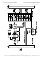
All logic to control data acquisition is imbedded in the IOS’s
FPGA. The control logic of the IOS-330 is responsible for
controlling the operation of a user specified sequence of data
acquisitions. Once the IOS-330 has been configured, the control
logic performs the following:
Controls the channel multiplexers based upon start and
end channel values, and single ended or differential
analog input mode.
Selects channel gain at the programmable gain amplifier
corresponding to the current channel.
Controls data conversion at the A/D Converter based on
one of five different scan modes of operation.
Controls data transfer from the A/D Converter to the
FPGA’s 16-bit serial shift register.
Controls and updates the Mailbox buffer, New Data
register, and Missed Data register.
Stops data acquisition for Single Cycle Scan modes.
Provides external or internal trigger control.
Controls the interval between data conversions.
Issues interrupt requests to the carrier.
INTERNAL CHANNEL POINTERS
Internal counters in the FPGA are used as pointers to: control
the multiplexers for selection of the current channel’s analog
signal; select and set the current channel’s Gain; and control
update of the Mailbox RAM buffer. The start channel register
controls the value at which these counters start, and the end value
register controls the maximum channel number which is reached.
In the continuous modes of operation these counters
continuously cycle, in sequential order, from the defined start value
to the defined end value. When the continuous mode of operation
is halted by disabling the scan mode via the control register, the
internal hardware counter remains at the count value reached
when halted. Upon start of a new scan mode, via the software
start convert bit or external trigger, the internal pointers are
reinitialized. Thus, the first channel converted, upon restart of data
conversions, will correspond to that set in the start value register.
A 16-bit serial shift register is implemented in the IOS’s FPGA.
This serial shift register interfaces to the A/D Converter. A clock
signal provided by the converter is used to serially shift the new
data from the converter to the FPGA’s 16-bit serial shift register.
Use of the converter’s clock signal (instead of an external clock)
minimizes the danger of digital noise feeding through and
corrupting the results of a conversion in process.
The converted data serially shifted, from the A/D Converter to
the FPGA, represents the analog signal digitized in the previous
convert cycle. That is, the A/D Converter transfers digitized
Upon initiation of an A/D convert cycle, the analog input data is
digitized and stored into an internal A/D Converter buffer. Also
during this cycle, the last converted data value is moved from the
A/D Converter buffer to the FPGA’s Mailbox Buffer. At this time
the New Data Available bit corresponding to the previous
converted channel is set in the FPGA register.
For all other scan modes the FPGA control logic will
automatically discard the first digitized data value received from
the A/D Converter. It is not written to the Mailbox buffer. In
addition, the FPGA logic also automatically generates the required
“flush” convert signals to obtain the last converted data value from
the A/D Converter.
EXTERNAL TRIGGER
The external trigger connection is made via pin 49 of the P2
Field I/O Connector. For the Burst and Continuous scan modes
the falling edge of the external trigger will start data acquisition
which will then be controlled by the FPGA. For External Trigger
Only mode, each falling edge of the external trigger causes a
conversion at the A/D Converter. Once the external trigger signal
has been driven low, it should remain low for minimum of 500n
seconds.
TIMED PERIODIC TRIGGER CIRCUIT
Timed Periodic Triggering is provided by two programmable
counters (an 8-bit Timer Prescaler and a 16-bit Conversion Timer).
The Timer Prescaler is clocked by the 8MHz. board clock. The
output of the Timer Prescaler counter is then used to clock the
second counter (Conversion Timer). In this way, the two counters
are cascaded to provide variable time periods anywhere from
8 sec to 2.0889 seconds. The output of the second counter is
used to trigger the start of new A/D conversions for the Uniform
Scan modes of operation. For the Burst Continuous mode, the
interval between conversions of each channel is fixed at 15 sec.
However, the interval between the group (burst) of channels can
be controlled by the Interval Timer.
INTERRUPT CONTROL LOGIC
The IOS-330 can be configured to generate an interrupt after
completion of conversion of a single channel or after conversion of
a group of channels is completed. IOS interrupt signal INTREQ0*
is issued to the carrier to request an interrupt. The interrupt
release mechanism employed is ROAK (Release On
Acknowledge). The IOS-330 will release the INTREQ0* signal
during an interrupt acknowledge cycle from the carrier.
- 17 Acromag, Inc. Tel:248-295-0310 Fax:248-624-9234 Email:[email protected] http://www.acromag.com