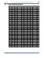
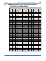
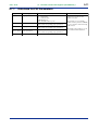
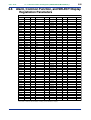
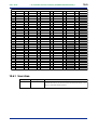
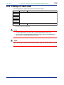
1
User’s
Manual
GREEN Series
Communication Reference
IM 05G01B02-02E
IM 05G01B02-02E
7th Edition
Blank Page
<Toc> <Ind> <Rev>
i
<Introduction>
Introduction
This user’s manual provides information about internal registers, which is required to
implement communication with the GREEN Series of controllers.
The GREEN Series have the following internal registers.
1) D registers
2) B registers <UP550 and UP750 only>
3) I relays
The GREEN Series controllers communicate with a higher-level device via these internal
registers.
You are required to understand the communication specifications of higher-level devices,
and have knowledge of the communication hardware, language used for creating communication programs, and so on.
* Higher-level devices: PCs, PLCs (sequencers), graphic panels, and others
■ Intended Readers
This manual is intended for people familiar with the functions of the GREEN Series controllers such as control engineers and personnel in charge of the maintenance of instrumentation and control equipment.
■ Related Documents
The following user’s manuals all relate to the communication functions of the GREEN
Series.
Read them as necessary. The codes enclosed in parentheses are the document numbers.
• UT350/UT320 User’s Manual
(IM 05D01D02-01E to 03E)
Explains the basic operation of the UT350/UT320 controller.
• UT351/UT321 User’s Manual
(IM 05D01D12-01E to 04E)
Explains the basic operation of the UT351/UT321 controller.
• UT450/UT420 User’s Manual
(IM 05D01C12-01E to 04E)
Explains the basic operation of the UT450/UT420 controller.
• UT550/UT520 User’s Manual for Single-loop Control
(IM 05D01C02-01E to 05E)
Explains the basic operation of the UT550/UT520 controller.
Media No. IM 05G01B02-02E
7th Edition : May 2006 (YK)
All Rights Reserved Copyright © 2000, Yokogawa Electric Corporation
IM 05G01B02-02E
7th Edition : 2006.05.31-00
<Toc> <Ind> <Rev>
ii
<Introduction>
• UT551 with embedded Ethernet User’s Manual for Single-loop Control
(IM 05D01C03-01E to 06E)
Explains the basic operation of the UT551 controller.
• UT551 User’s Manual for Single-loop Control
(IM 05D01C04-01E to 06E)
Explains the basic operation of the UT551 controller.
• UT750 User’s Manual for Single-loop Control
(IM 05D01B02-01E to 05E)
Explains the basic operation of the UT750 controller.
• UP350 User’s Manual
(IM 05E01D02-01E to 04E)
Explains the basic operation of the UP350 controller.
• UP351 User’s Manual
(IM 05E01D12-01E to 05E)
Explains the basic operation of the UP351 controller.
• UP550 User’s Manual for Single-loop Control
(IM 05E01C02-01E to 07E)
Explains the basic operation of the UP550 controller.
• UP750 User’s Manual for Single-loop Control
(IM 05E01B02-01E to 07E)
Explains the basic operation of the UP750 controller.
• UM350/UM330 User’s Manual
(IM 05F01D02-01E to 03E)
Explains the basic operation of the UM350/UM330 indicator.
• UM351/UM331 User’s Manual
(IM 05F01D12-01E to 04E)
Explains the basic operation of the UM351/UM331 indicator.
• GREEN Series User’s Manual - Detailed Instructions
(IM 05J01B02-01E)
Explains the functions of the GREEN Series controllers in detail.
• GREEN Series Communication Function
(IM 05G01B02-01E)
Provides detailed information about the GREEN Series controller’s communication protocol.
IM 05G01B02-02E
7th Edition : 2006.05.31-00
<Toc> <Ind> <Rev>
iii
<Introduction>
• GREEN Series Communication Reference
(IM 05G01B02-02E)
Provides detailed information about the GREEN Series controller’s internal registers that
can be accessed by communication.
• LL100 PC-based Parameters Setting Tool
(IM 05G01B12-01E)
A user’s manual for setting the parameters of the GREEN Series controllers from a personal computer.
• LL200 PC-based Custom Computation Building Tool
(IM 05G01B22-01E)
A user’s manual for creating GREEN Series custom computations on a personal computer.
• LL200 PC-based Custom Computation Building Tool User’s Reference
(for UT750: IM 05G01B22-02E)
(for UP750: IM 05G01B22-03E)
An user’s manual that describes the functions needed to create GREEN Series custom
computations. Refer to this manual if you are not familiar with the types of functions available or how these functions work.
• Ethernet Communication Functions User’s Manual
(IM 05G01B52-01E)
Provides detailed information about the Ethernet communication functions, communication
protocol and D registers.
■ Trademarks
Windows98/2000/XP and Windows NT 4.0 are registered trademarks of Microsoft Corporation, USA.
IM 05G01B02-02E
7th Edition : 2006.05.31-00
<Toc> <Ind> <Rev>
iv
<Introduction>
Documentation Conventions
■ Symbols
WARNING
Indicates that operating the hardware or software in this manner may damage it or lead to
system failure.
NOTE
Draws attention to information that is essential for understanding the operation and/or
features of the product.
TIP
Gives additional information to complement the present topic.
See Also
Gives reference locations for further information on the topic.
■ Description of Displays
(1) Some of the representations of product displays shown in this manual may be exaggerated, simplified, or partially omitted for reasons of convenience when explaining them.
(2) Figures and illustrations representing the controller’s displays may differ from the real
displays in regard to the position and/or indicated characters (upper-case or lowercase, for example), to the extent that they do not impair a correct understanding of the
functions and the proper operation and monitoring of the system.
IM 05G01B02-02E
7th Edition : 2006.05.31-00
<Toc> <Ind> <Rev>
v
<Introduction>
Notices
■ Regarding This User’s Manual
(1) This manual should be passed on to the end user. Keep at least one extra copy of the
manual in a safe place.
(2) Read this manual carefully to gain a thorough understanding of how to operate this
product before you start using it.
(3) This manual is intended to describe the functions of this product. Yokogawa Electric
Corporation (hereinafter simply referred to as Yokogawa Electric) does not guarantee
that these functions are suited to the particular purpose of the user.
(4) Under absolutely no circumstance may the contents of this manual, in part or in whole,
be transcribed or copied without permission.
(5) The contents of this manual are subject to change without prior notice.
(6) Every effort has been made to ensure accuracy in the preparation of this manual.
Should any errors or omissions come to your attention, however, please contact your
nearest Yokogawa representative or our sales office.
■ Regarding Protection, Safety, and Prohibition Against Unauthorized
Modification
In order to protect the product and the system controlled by it against damage and ensure
its safe use, make certain that all of the instructions and precautions relating to safety
contained in this document are strictly adhered to. Yokogawa Electric does not guarantee
safety if products are not handled according to these instructions.
■ Force Majeure
(1) Yokogawa Electric does not make any warranties regarding the product except those
mentioned in the WARRANTY that is provided separately.
(2) Yokogawa Electric assumes no liability to any party for any loss or damage, direct or
indirect, caused by the use or any unpredictable defect of the product.
(3) Be sure to use the spare parts approved by Yokogawa Electric when replacing parts or
consumables.
(4) Modification of the product is strictly prohibited.
(5) Use this software with one specified computer only. You must purchase another copy of
the software for use on each additional computer.
(6) Copying this software for purposes other than backup is strictly prohibited.
(7) Store the floppy disk(s) (original medium or media) containing this software in a secure
place.
(8) Reverse engineering such as the disassembly or decompilation of software is strictly
prohibited.
(9) No portion of the software supplied by Yokogawa Electric may be transferred, exchanged, leased or sublet for use by any third party without the prior permission of
Yokogawa Electric.
■ Trademark
“Ethernet” is registered trademark of XEROX Corporation.
IM 05G01B02-02E
7th Edition : 2006.05.31-00
Blank Page
Toc-i
<Int> <Ind> <Rev>
GREEN Series
Communication Reference
IM 05G01B02-02E 7th Edition
CONTENTS
Introduction........................................................................................................... i
Documentation Conventions ..............................................................................iv
Notices ................................................................................................................. v
1.
Functions and Use of D Registers (UT750/UT550/UT520/UT551) ......... 1-1
1.1
Overview .......................................................................................................... 1-1
1.2
Interpretation of D Register Tables ................................................................ 1-1
1.3
Classification of D Registers .......................................................................... 1-2
1.4
Process Data and User Area .......................................................................... 1-3
1.5
1.6
1.4.1
Process Data Area (Read-only) ........................................................ 1-4
1.4.2
User Area ....................................................................................... 1-12
Operation Mode and Computation Parameters .......................................... 1-13
1.5.1
Operation Mode Information ........................................................... 1-14
1.5.2
Write-only Data Area ....................................................................... 1-15
1.5.3
Data Area for Computation Parameters .......................................... 1-16
Loop-1 PID Parameters ................................................................................. 1-17
1.6.1
1.7
Loop-2 PID Parameters ................................................................................. 1-20
1.7.1
1.8
1.9
1.10
Data Area for Loop-1 PID Parameters ............................................. 1-19
Data Area for Loop-2 PID Parameters ............................................. 1-22
USER Parameters, Ten-segment Linearizer Parameters, and Messages .. 1-23
1.8.1
Data Area for USER Parameters ..................................................... 1-25
1.8.2
Data Area for Parameters of Ten-segment Linearizers 1 and 2 ........ 1-25
1.8.3
Area for Message ........................................................................... 1-26
Control Action, Loop-common Function, and I/O Configuration Parameters ... 1-27
1.9.1
Data Area for Control Action Parameters ......................................... 1-30
1.9.2
Data Area for Loop-common Function Parameters ......................... 1-30
1.9.3
Data Area for I/O Configuration Parameters .................................... 1-30
Controller Mode (UT mode), PV Input, and Control Output Parameters .... 1-31
1.10.1
Data Area for Controller Mode (UT mode), PV Input, and
Control Output Parameters ............................................................. 1-32
1.11
Input Block Area for Custom Computation (UT750 only) ........................... 1-33
1.12
Output Block Area for Custom Computation (UT750 only) ........................ 1-35
IM 05G01B02-02E
7th Edition : 2006.05.31-00
Toc-ii
<Int> <Ind> <Rev>
2.
Functions and Use of D Registers (UT450/UT420) ................................ 2-1
2.1
Overview .......................................................................................................... 2-1
2.2
Interpretation of D Register Tables ................................................................ 2-1
2.3
Classification of D Registers .......................................................................... 2-2
2.4
Process Data and User Area .......................................................................... 2-3
2.5
2.6
2.4.1
Process Data Area (Read-only) ........................................................ 2-4
2.4.2
User Area ......................................................................................... 2-8
Operation Mode and Computation Parameters ............................................ 2-9
2.5.1
Operation Mode Information ........................................................... 2-10
2.5.2
Write-only Data Area ....................................................................... 2-10
2.5.3
Data Area for Computation Parameters ........................................... 2-11
PID Parameters ............................................................................................. 2-12
2.6.1
2.7
2.8
Control Action, Common Function, and SELECT Display Registration
Parameters .................................................................................................... 2-15
2.7.1
Data Area for Control Action Parameters ......................................... 2-18
2.7.2
Data Area for Common Function Parameters .................................. 2-18
2.7.3
Data Area for SELECT Display Registration Parameters ................. 2-18
PV Input, Control Output, and Communication Parameters ...................... 2-19
2.8.1
3.
Data Area for PID Parameters ........................................................ 2-14
Data Area for PV Input, Control Output, and Communication Parameters .. 2-20
Functions and Use of D Registers (UT350/UT320,UT351/UT321) ......... 3-1
3.1
Overview .......................................................................................................... 3-1
3.2
Interpretation of D Register Tables ................................................................ 3-1
3.3
Classification of D Registers .......................................................................... 3-2
3.4
Process Data and User Area .......................................................................... 3-3
3.5
3.6
3.4.1
Process Data Area (Read-only) ........................................................ 3-4
3.4.2
User Area ......................................................................................... 3-6
Operation Mode and Computation Parameters ............................................ 3-7
3.5.1
Operation Mode Information ............................................................. 3-8
3.5.2
Write-only Data Area ......................................................................... 3-8
3.5.3
Data Area for Computation Parameters ............................................ 3-9
PID Parameters ............................................................................................. 3-10
3.6.1
3.7
3.8
Data Area for PID Parameters ......................................................... 3-11
Control Action, Common Function, and SELECT Display Registration
Parameters .................................................................................................... 3-12
3.7.1
Data Area for Control Action Parameters ......................................... 3-15
3.7.2
Data Area for Common Function Parameters .................................. 3-15
3.7.3
Data Area for SELECT Display Registration Parameters ................. 3-15
PV Input, Control Output, and Communication Parameters ...................... 3-16
3.8.1
Data Area for PV Input, Control Output, and Communication Parameters .. 3-17
IM 05G01B02-02E
7th Edition : 2006.05.31-00
Toc-iii
<Int> <Ind> <Rev>
4.
Functions and Use of D Registers (UP750/UP550) ................................ 4-1
4.1
Overview .......................................................................................................... 4-1
4.2
Interpretation of D Register Tables ................................................................ 4-1
4.3
Classification of D Registers .......................................................................... 4-2
4.4
Process Data and User Area .......................................................................... 4-3
4.4.1
Process Data Area (Read-only) ........................................................ 4-4
4.4.2
User Area ....................................................................................... 4-13
4.5
Program Data ................................................................................................ 4-14
4.6
Operation Mode and Computation Parameters .......................................... 4-15
4.7
4.6.1
Operation Mode Information ........................................................... 4-16
4.6.2
Write-only Data Area ....................................................................... 4-17
4.6.3
Data Area for Computation Parameters .......................................... 4-17
Loop-1 PID Parameters ................................................................................. 4-18
4.7.1
4.8
Loop-2 PID Parameters ................................................................................. 4-21
4.8.1
4.9
4.10
4.11
Data Area for Loop-1 PID Parameters ............................................. 4-20
Data Area for Loop-2 PID Parameters ............................................. 4-23
USER Parameters, Ten-segment Linearizer Parameters, and Messages .. 4-24
4.9.1
Data Area for USER Parameters ..................................................... 4-26
4.9.2
Data Area for Parameters of Ten-segment Linearizers 1 and 2 ........ 4-26
4.9.3
Area for Message ........................................................................... 4-27
Control Action, Loop-common Function, and I/O Configuration Parameters ... 4-28
4.10.1
Data Area for Control Action Parameters ......................................... 4-31
4.10.2
Data Area for Loop-common Function Parameters ......................... 4-31
4.10.3
Data Area for I/O Configuration Parameters .................................... 4-31
Controller Mode (UP mode), PV Input, and Control Output Parameters .... 4-32
4.11.1
Data Area for Controller Mode (UP mode), PV Input, and
Control Output Parameters ............................................................. 4-33
4.12
Input Block Area for Custom Computation (UP750 only) ........................... 4-34
4.13
Output Block Area for Custom Computation (UP750 only) ........................ 4-36
IM 05G01B02-02E
7th Edition : 2006.05.31-00
Toc-iv
<Int> <Ind> <Rev>
5.
Functions and Use of D Registers (UP350/UP351) ................................ 5-1
5.1
Overview .......................................................................................................... 5-1
5.2
Interpretation of D Register Tables ................................................................ 5-1
5.3
Classification of D Registers .......................................................................... 5-2
5.4
Process Data and User Area .......................................................................... 5-3
5.4.1
Process Data Area (Read-only) ........................................................ 5-4
5.4.2
User Area ......................................................................................... 5-5
5.5
Program Parameters ....................................................................................... 5-6
5.6
Operation Mode and Computation Parameters ............................................ 5-7
5.7
5.6.1
Operation Mode Information ............................................................. 5-8
5.6.2
Write-only Data Area ......................................................................... 5-8
5.6.3
Data Area for Computation Parameters ............................................ 5-8
PID Parameters ............................................................................................... 5-9
5.7.1
5.8
5.9
Control Action, Common Function, and SELECT Display Registration
Parameters .................................................................................................... 5-12
5.8.1
Data Area for Control Action Parameters ......................................... 5-15
5.8.2
Data Area for Common Function Parameters .................................. 5-15
5.8.3
Data Area for SELECT Display Registration Parameters ................. 5-15
PV Input, Control Output, and Communication Parameters ...................... 5-16
5.9.1
6.
Data Area for PID Parameters ......................................................... 5-11
Data Area for PV Input, Control Output, and Communication Parameters .. 5-17
Functions and Use of D Registers (UM350/UM330,UM351/UM331) ...... 6-1
6.1
Overview .......................................................................................................... 6-1
6.2
Interpretation of D Register Tables ................................................................ 6-1
6.3
Classification of D Registers .......................................................................... 6-2
6.4
Process Data and User Area .......................................................................... 6-3
6.5
6.4.1
Process Data Area (Read-only) ........................................................ 6-4
6.4.2
User Area ......................................................................................... 6-5
Computation Parameters ............................................................................... 6-6
6.5.1
6.6
6.7
Data Area for Alarm Setpoint, Computation, and PV-related Parameters ... 6-7
Alarm, Common Function, and SELECT Display Registration Parameters ... 6-8
6.6.1
Data Area for Alarm-related Parameters .......................................... 6-11
6.6.2
Data Area for Common Function Parameters ................................... 6-11
6.6.3
Data Area for SELECT Display Registration Parameters .................. 6-11
PV Input and Communication Parameters .................................................. 6-12
6.7.1
Data Area for PV Input and Communication Parameters ................. 6-13
IM 05G01B02-02E
7th Edition : 2006.05.31-00
Toc-v
<Int> <Ind> <Rev>
7.
Functions and Use of B Registers (UP750/UP550) ................................ 7-1
7.1
Overview .......................................................................................................... 7-1
7.2
Interpretation of B Register Tables ................................................................ 7-1
7.3
Classification of B Registers .......................................................................... 7-2
7.4
Program Pattern and Segment Data .............................................................. 7-3
7.4.1
7.5
Final Target Setpoint (TSP) Data .................................................................... 7-8
7.6
Using B Registers .......................................................................................... 7-11
7.7
8.
9.
7.6.1
Reading/Writing the Start Condition Data ......................................... 7-11
7.6.2
Reading/Writing the Segment Data and Event Data ........................ 7-12
7.6.3
Reading the Numbers of Remaining Segments and Remaining Events . 7-13
7.6.4
Copying, Deleting, and Reading a Program Pattern ........................ 7-14
Error Indication at Program Pattern Creation and Editing ......................... 7-15
Functions and Use of I Relays (UT750/UT550/UT520/UT551) ............... 8-1
8.1
Overview .......................................................................................................... 8-1
8.2
Classification of I Relays ................................................................................ 8-1
8.3
Status I Relays ................................................................................................ 8-2
8.4
ON-Status I Relays .......................................................................................... 8-4
8.5
OFF-Status I Relays ........................................................................................ 8-6
8.6
Status I Relays for Alarm, Timer, Power-on Flags, Reverse Status, and Others... 8-8
8.6.1
User Area ........................................................................................ 8-11
8.6.2
Timer Function ................................................................................. 8-11
Functions and Use of I Relays (UT450/UT420) ...................................... 9-1
9.1
Overview .......................................................................................................... 9-1
9.2
Classification of I Relays ................................................................................ 9-1
9.3
Status I Relays ................................................................................................ 9-2
9.4
ON-Status I Relays .......................................................................................... 9-4
9.5
OFF-Status I Relays ........................................................................................ 9-6
9.6
I Relays in User Area ....................................................................................... 9-8
9.6.1
10.
Program Pattern Information ............................................................. 7-5
User Area ......................................................................................... 9-9
Functions and Use of I Relays (UT350/UT320,UT351/UT321) ............. 10-1
10.1
Overview ........................................................................................................ 10-1
10.2
Classification of I Relays .............................................................................. 10-1
10.3
Status I Relays .............................................................................................. 10-2
10.4
ON-Status I Relays ........................................................................................ 10-4
10.5
OFF-Status I Relays ...................................................................................... 10-6
10.6
Status I Relays in User Area ......................................................................... 10-8
10.6.1
User Area ....................................................................................... 10-9
IM 05G01B02-02E
7th Edition : 2006.05.31-00
Toc-vi
<Int> <Ind> <Rev>
11.
12.
Functions and Use of I Relays (UP750/UP550) ..................................... 11-1
11.1
Overview ......................................................................................................... 11-1
11.2
Classification of I Relays ............................................................................... 11-1
11.3
Status I Relays ...............................................................................................11-2
11.4
ON-Status I Relays .........................................................................................11-4
11.5
OFF-Status I Relays ....................................................................................... 11-6
11.6
Status I Relays for Alarm, Timer, and Power-on Flags, and Others ............ 11-8
11.6.1
User Area ........................................................................................ 11-9
11.6.2
Timer Function ............................................................................... 11-10
Functions and Use of I Relays (UP350/UP351) .................................... 12-1
12.1
Overview ........................................................................................................ 12-1
12.2
Classification of I Relays .............................................................................. 12-1
12.3
Status I Relays .............................................................................................. 12-2
12.4
ON-Status I Relays ........................................................................................ 12-4
12.5
OFF-Status I Relays ...................................................................................... 12-6
12.6
I Relays in User Area ..................................................................................... 12-8
12.6.1
13.
User Area ....................................................................................... 12-9
Functions and Use of I Relays (UM350/UM330,UM351/UM331) .......... 13-1
13.1
Overview ........................................................................................................ 13-1
13.2
Classification of I Relays .............................................................................. 13-1
13.3
Status I Relays .............................................................................................. 13-2
13.4
ON-Status I Relays ........................................................................................ 13-4
13.5
OFF-Status I Relays ...................................................................................... 13-6
13.6
I Relays in User Area ..................................................................................... 13-8
13.6.1
User Area ....................................................................................... 13-9
Revision Information ............................................................................................ i
IM 05G01B02-02E
7th Edition : 2006.05.31-00
<Toc> <Ind>
1-1
<1. Functions and Use of D Registers (UT750/UT550/UT520/UT551) >
1.
Functions and Use of D Registers
(UT750/UT550/UT520/UT551)
1.1
Overview
This section explains the functions and use of D registers.
D registers store parameter data, flag data and process data of a GREEN Series controller.
You can readily use these internal data items by reading from or writing to the D registers.
You can use D registers to perform:
● Centralized control using a higher-level device
● Data exchange by reading/writing data from/to a higher-level device
1.2
Interpretation of D Register Tables
This section explains how to read the D Register Map tables in this chapter. The numbers
listed in the leftmost column are D register numbers ((1) below). The five-digit numbers in
the next column are reference numbers used for MODBUS communication ((2) below).
The numbers in the column third from left are register numbers in hexadecimal notation
used in MODBUS communication programs ((3) below). Each register code name in the D
Register Map tables represents a specific process data item, operation parameter, setup
parameter or other data items such as a flag. For details on the operation parameters and
setup parameters, see the user’s manual of UT750/UT550/UT520/UT551.
Name of D Register Map
D-Reg No.
Ref No.
H No.
Register name
R/W
D0001
40001
0000
ADERROR
R
(1) D register number
(3) Hex number
(for MODBUS communication
program)
Permission of read/write by communication
An asterisk (*) in this column indicates that the
number of writing actions is limited to 100,000.
(2) Reference number (for MODBUS communication)
■ Names of D Registers
The base names of some D registers are preceded by a combination of a number and then
a period, and/or followed by a combination of a period and then a number, as shown in the
format Y.
.X. (Y: group number; X: loop number)
Examples:
• The name 3.SP.1 means the SP of group 3 and for Loop-1.
• The name OUT.2 means the OUT of Loop-2.
IM 05G01B02-02E
7th Edition : 2006.05.31-00
<Toc> <Ind>
1.3
1-2
<1. Functions and Use of D Registers (UT750/UT550/UT520/UT551) >
Classification of D Registers
■ Classification of D Register Map Tables
The table below outlines how the D registers are classified by their numbers in the D
Register Map tables.
Table 1.1 Classification of D Registers
Register No.
Area and data categories
D0001 to D0049 Process data area (Note 1)
Data displayed for operation
D0050 to D0100 User area (Note 2),
represented by shaded cells in
the table
_
Description
Reference
PV, SP, OUT, and others
Section 1.4
If a graphic panel is used, this area is Section 1.4
used for communication with the
graphic panel.
D0101 to D0200 Cannot be used
D0201 to D0230 Operation parameters (Note 1) Operation mode parameters
A/M, C/A/M, MOUT, and others
Section 1.5
D0231 to D0300
Operation-related parameters for
Loop-1 and -2
AT, SC, BS, FL, and others
Sections 1.6
and 1.7
PID parameters for Loop-1 and -2
P, I, D, and others
Sections 1.6
and 1.7
D0301 to D0700
D0701 to D0800 Operation parameters
Ten-segment linearizer parameters and 1.A1 to 1.PMD and others
USER parameters
D0801 to D0900 Display messages
Message texts
Display messages (each comprising
up to 20 alphanumeric characters)
Section 1.8
D0901 to D1000 Setup parameters (Note 1)
Control action parameters for Loop-1
and -2
SP, ALM, CTL
Section 1.9
D1001 to D1100
Loop-common function parameters
AIN, RET, TRND, LOCK
Section 1.9
D1101 to D1200
Display and I/O configuration
parameters
CSEL, DO, DI, C.PYS
Section 1.9
Controller mode, PV input, and
control output parameters
UTMD, IN, OUT, R485, INIT
Section 1.10
Input block
Block input/output and module
output
Sections 1.11
and 1.12
D1201 to D1300
D1301 to D1500 User definitions (custom
computation area)
D1501 to D1700
Output block
Section 1.8
Note 1: Data for process values, operation parameters and setup parameters are stored in the types (PV input range, PV input range span, %, or
ABS without the decimal point) indicated in the Operation Parameter Lists and Setup Parameter Lists of the user s manual of
UT750/UT550/UT520/UT551. The OFF and ON states are represented by 0 and 1, respectively. D registers D0001 to D0049 are readonly.
Note 2: When communicating with a graphic panel, do not write to or read from this area (D0050 to D0100) because this area is reserved for 16bit register data used by graphic panels.
NOTE
It is prohibited to read/write data by communication from/to the registers of blank cells in the
register map tables. If you attempt to do so, the UT750/UT550/UT520/UT551 may not
operate properly.
IM 05G01B02-02E
7th Edition : 2006.05.31-00
<Toc> <Ind>
1.4
1-3
<1. Functions and Use of D Registers (UT750/UT550/UT520/UT551) >
Process Data and User Area
Area for process data
D-Reg No. Ref No.
D0001
D0002
D0003
D0004
D0005
D0006
D0007
D0008
D0009
D0010
D0011
D0012
D0013
D0014
D0015
D0016
D0017
D0018
D0019
D0020
D0021
D0022
D0023
D0024
D0025
D0026
D0027
D0028
D0029
D0030
D0031
D0032
D0033
D0034
D0035
D0036
D0037
D0038
D0039
D0040
D0041
D0042
D0043
D0044
D0045
D0046
D0047
D0048
D0049
D0050
Shaded area
H No.
Register name
40001
40002
40003
40004
40005
40006
40007
40008
40009
40010
40011
0000
0001
0002
0003
0004
0005
0006
0007
0008
0009
000A
ADERROR
ERROR.1
PV.1
CSP.1
OUT.1
HOUT.1
COUT.1
MOD.1
PIDNO.1
CSPNO
ALM
R/ W
R
R
R
R
R
R
R
R
R
R
R
40018
40019
40020
40021
40022
40023
40024
40025
40026
40027
0011
0012
0013
0014
0015
0016
0017
0018
0019
001A
ERROR.2
PV.2
CSP.2
OUT.2
HOUT.2
COUT.2
MOD.2
PIDNO.2
DEV.1
OR.1
R
R
R
R
R
R
R
R
R
R
40030
40031
40032
40033
40034
40035
40036
40037
40038
40039
40040
001D
001E
001F
0020
0021
0022
0023
0024
0025
0026
0027
DEV.2
OR.2
SMEC
DISTS
RDISTS
PARAERR
ALOSTS
TIM1
TIM2
DISP1
DISP2
R
R
R
R
R
R
R
R
R
R
R
40050
0031
R/W
D-Reg No. Ref No.
D0051
D0052
D0053
D0054
D0055
D0056
D0057
D0058
D0059
D0060
D0061
D0062
D0063
D0064
D0065
D0066
D0067
D0068
D0069
D0070
D0071
D0072
D0073
D0074
D0075
D0076
D0077
D0078
D0079
D0080
D0081
D0082
D0083
D0084
D0085
D0086
D0087
D0088
D0089
D0090
D0091
D0092
D0093
D0094
D0095
D0096
D0097
D0098
D0099
D0100
40051
40052
40053
40054
40055
40056
40057
40058
40059
40060
40061
40062
40063
40064
40065
40066
40067
40068
40069
40070
40071
40072
40073
40074
40075
40076
40077
40078
40079
40080
40081
40082
40083
40084
40085
40086
40087
40088
40089
40090
40091
40092
40093
40094
40095
40096
40097
40098
40099
40100
H No.
Register name
0032
0033
0034
0035
0036
0037
0038
0039
003A
003B
003C
003D
003E
003F
0040
0041
0042
0043
0044
0045
0046
0047
0048
0049
004A
004B
004C
004D
004E
004F
0050
0051
0052
0053
0054
0055
0056
0057
0058
0059
005A
005B
005C
005D
005E
005F
0060
0061
0062
0063
R/ W
R/W
R/W
R/W
R/W
R/W
R/W
R/W
R/W
R/W
R/W
R/W
R/W
R/W
R/W
R/W
R/W
R/W
R/W
R/W
R/W
R/W
R/W
R/W
R/W
R/W
R/W
R/W
R/W
R/W
R/W
R/W
R/W
R/W
R/W
R/W
R/W
R/W
R/W
R/W
R/W
R/W
R/W
R/W
R/W
R/W
R/W
R/W
R/W
R/W
R/W
: User area (You cannot use these registers when a graphic panel is used.)
IM 05G01B02-02E
7th Edition : 2006.05.31-00
<Toc> <Ind>
1.4.1
1-4
<1. Functions and Use of D Registers (UT750/UT550/UT520/UT551) >
Process Data Area (Read-only)
Some of the registers in this area (D0001 to D0049, read-only) are designed to represent
two or more events, such as errors and statuses, using combinations of bits within the
register. If any of the events shown in the following tables occur, the corresponding bit is set
to 1. The bit remains 0 if the event does not occur. Note that bits with blank fields in the
tables are not in use.
● Bit Configuration of D0001: ADERROR (Input Error)
Bit
Code
Event
0
1
2
3
4
5
6
7
8
9
10 to 15
AD1ERR.st
AD2ERR.st
AD3ERR.st
Input-1 A/D converter error
Input-2 A/D converter error (UT750 only)
Input-3 A/D converter error
AD1BO.st
AD2BO.st
AD3BO.st
Input-1 burnout error
Input-2 burnout error (UT750 only)
Input-3 burnout error
RJC1ERR.st
RJC2ERR.st
Input-1 RJC error
Input-2 RJC error (UT750 only)
● Bit Configuration of D0002: ERROR.1 (PV1 Error)
Bit
Code
Event
0
1
2
3
4
5
6, 7
8
9
10, 11
12
13
14
15
PV1ADC.st
PV1BO.st
RJC1ERR.st
PV1 A/D converter error
PV1 burnout error
PV1 RJC error
PV1+over.st
PV1-over.st
PV1 over-scale
PV1 under-scale
RSP1ADC.st
RSP1BO.st
RSP1 A/D converter error
RSP1 burnout error
C.RSP1ADC.st
C.RSP1BO.st
AT1ERR.st
RSP1 A/D converter error when RSP1 is used for control
Burnout error when RSP1 is used for control
Auto-tuning error
● D0003: PV.1 (Measured input value [PV] for Loop-1)
● D0004: CSP.1 (Current target setpoint [SP] for Loop-1)
IM 05G01B02-02E
7th Edition : 2006.05.31-00
<Toc> <Ind>
1-5
<1. Functions and Use of D Registers (UT750/UT550/UT520/UT551) >
● D0005: OUT.1 (Control output value [OUT] for Loop-1)
• During PID computation, you can read the computation result as is from this register.
For example, when the computation result is 75.0%, the register contains a value of
“750.”
• During on-off computation, the register contains “0” (0.0%) for the OFF state or “1000”
(100.0%) for the ON state.
• During heating/cooling computation, this register contains a value half the PID computation result.
● D0006: HOUT.1 (Heating-side control output for Loop-1 in Heating/Cooling
Control)
• During heating/cooling computation, this register contains the heating-side control
output value.
● D0007: COUT.1 (Cooling-side control output for Loop-1 in Heating/Cooling
Control)
• During heating/cooling computation, this register contains the cooling-side control
output value.
● Bit Configuration of D0008: MOD.1 (Operation mode of Loop-1)
Bit
Code
Event
0
1
2
3
4
5
6
7 to 13
14
15
A/M1.st
R/L1.st
R/S1.st
0: AUTO; 1: MAN
0: Local; 1: Remote
0: Run; 1: Stop
CAS.st
AUT.st
MAN.st
1: CAS
1: AUTO
1: MAN
AT1.st
0: Auto-tuning is OFF; 1: Auto-tuning is ON
● D0009: PIDNO.1 (Current PID number for Loop-1)
Bit
Code
Event
0
1
2
3
4 to 15
PIDNO.0
PIDNO.1
PIDNO.2
PIDNO.3
Bit
Bit
Bit
Bit
0
1
2
3
of
of
of
of
the
the
the
the
current
current
current
current
PID
PID
PID
PID
number
number
number
number
From this register, you can read the PID number currently in use in the form of a binary bit
string. For example, the configuration of “bit 3 = off; bit 2 = on; bit 1 = off; bit 0 = on”, which
is represented as “0101” in binary notation and as “5” in decimal notation, indicates that the
PID number currently being used is 5.
IM 05G01B02-02E
7th Edition : 2006.05.31-00
<Toc> <Ind>
1-6
<1. Functions and Use of D Registers (UT750/UT550/UT520/UT551) >
● D0010: CSPNO (Current target-setpoint number)
Bit
Code
Event
0
1
2
3
4 to 15
CSPNO1.0
CSPNO1.1
CSPNO1.2
CSPNO1.3
Bit 0 of CSP (current SP number)
Bit 1 of CSP (current SP number)
Bit 2 of CSP (current SP number)
Bit 3 of CSP (current SP number)
From this register, you can read the SP number of the target setpoint currently being used
in the form of a binary bit string. For example, the configuration of “bit 3 = off; bit 2 = on; bit
1 = off; bit 0 = on”, which is represented as “0101” in binary notation and as “5” in decimal
notation, indicates that the target setpoint value of 5.SP is now being used.
● Bit Configuration of D0011: ALM (Alarm Status)
Bit
Code
Event
0
1
2
3
4
5
6, 7
8
9
10
11
12
13
14, 15
ALM11.st
ALM12.st
ALM13.st
‘1’ when alarm 1 for Loop-1 is ON; ‘0’ when OFF
‘1’ when alarm 2 for Loop-1 is ON; ‘0’ when OFF
‘1’ when alarm 3 for Loop-1 is ON; ‘0’ when OFF
ALM14.st
OR1.st
‘1’ when alarm 4 for Loop-1 is ON; ‘0’ when OFF
‘1’ when sensor grounding alarm for Loop-1 is ON; ‘0’ when OFF
ALM21.st
ALM22.st
ALM23.st
‘1’ when alarm 1 for Loop-2 is ON; ‘0’ when OFF
‘1’ when alarm 2 for Loop-2 is ON; ‘0’ when OFF
‘1’ when alarm 3 for Loop-2 is ON; ‘0’ when OFF
ALM24.st
OR2.st
‘1’ when alarm 4 for Loop-2 is ON; ‘0’ when OFF
‘1’ when sensor grounding alarm for Loop-2 is ON; ‘0’ when OFF
When the controller mode (UT mode) is other than “cascade control,” ALM21 to ALM24 for
Loop-2 are used as alarms 5 to 8 for Loop-1 if the 8-alarm mode is selected using setup
parameter AMD.
[See Also] The section on the 8-alarm mode in the User’s Manual of UT750/UT550/
UT520/UT551
IM 05G01B02-02E
7th Edition : 2006.05.31-00
<Toc> <Ind>
1-7
<1. Functions and Use of D Registers (UT750/UT550/UT520/UT551) >
● Bit Configuration of D0018: ERROR.2 (PV2 Error)
Bit
Code
Event
0
1
2
3
4
5
6, 7
8
9
10, 11
12
PV2ADC.st
PV2BO.st
RJC2ERR.st
PV2 A/D converter error
PV2 burnout error
PV2 RJC error (UT750 only)
PV2+over.st
PV2-over.st
PV2 over-scale
PV2 under-scale
RSP2ADC.st
RSP2BO.st
RSP2 A/D converter error (UT750 only)
RSP2 burnout error (UT750 only)
C.RSP2ADC.st
13
14
15
C.RSP2BO.st
AT2ERR.st
RSP2 A/D converter error when RSP1 is used for control
(UT750 only)
Burnout error when RSP2 is used for control (UT750 only)
Auto-tuning error
● D0019: PV.2 (Measured input value [PV] for Loop-2)
● D0020: CSP.2 (Current target setpoint [SP] for Loop-2)
● D0021: OUT.2 (Control output value [OUT] for Loop-2)
• During PID computation, you can read the computation result as is from this register.
For example, when the computation result is 75.0%, the register contains a value of
“750.”
• During on-off computation, the register contains “0” (0.0%) for the OFF state or “1000”
(100.0%) for the ON state.
• During heating/cooling computation, this register contains a value half the PID computation result.
● D0022: HOUT.2 (Heating-side control output for Loop-2 in Heating/Cooling
Control)
• During on-off computation, the register contains “0” (0.0%) for the OFF state or “1000”
(100.0%) for the ON state.
• During heating/cooling computation, this register contains the heating-side control
output value.
● D0023: COUT.2 (Cooling-side control output for Loop-2 in Heating/Cooling
Control)
• During on-off computation, the register contains “0” (0.0%) for the OFF state or “1000”
(100.0%) for the ON state.output value.
• During heating/cooling computation, this register contains the heating-side control
output value.
IM 05G01B02-02E
7th Edition : 2006.05.31-00
<Toc> <Ind>
1-8
<1. Functions and Use of D Registers (UT750/UT550/UT520/UT551) >
● Bit Configuration of D0024: MOD.2 (Operation mode of Loop-2)
Bit
Code
Event
0
1
2 to 13
14
15
A/M2.st
R/L2.st
0: AUTO; 1: MAN (UT750 only)
0: Local; 1: Remote (UT750 only)
AT2.st
0: Auto-tuning is OFF; 1: Auto-tuning is ON
● D0025: PIDNO.2 (Current PID number for Loop-2)
Bit
Code
Event
0
1
2
3
4 to 15
PIDNO2.0
PIDNO2.1
PIDNO2.2
PIDNO2.3
Bit
Bit
Bit
Bit
0
1
2
3
of
of
of
of
the
the
the
the
current
current
current
current
PID
PID
PID
PID
number
number
number
number
From this register, you can read the PID number currently in use in the form of a binary bit
string. For example, the configuration of “bit 3 = off; bit 2 = on; bit 1 = off; bit 0 = on”, which
is represented as “0101” in binary notation and as “5” in decimal notation, indicates that the
PID number currently being used is 5.
● D0026: DEV.1 (Deviation for Loop-1)
● D0027: OR.1 (Moving average of sensor grounding alarm for Loop-1)
● D0030: DEV.2 (Deviation for Loop-2)
● D0031: OR.2 (Moving average of sensor grounding alarm for Loop-2)
● D0032: SMEC (Sampling error counter).
IM 05G01B02-02E
7th Edition : 2006.05.31-00
<Toc> <Ind>
<1. Functions and Use of D Registers (UT750/UT550/UT520/UT551) >
1-9
● Bit Configuration of D0033: DISTS (Statuses of External Contact Inputs)
Bit
Code
Event
0
DI1.st
1
DI2.st
2
DI3.st
3
DI4.st
4
DI5.st
5
DI6.st
6
DI7.st
7
DI8.st
8
DP1
9
DP2
10
MG1
11
MG2
12
MG3
13
MG4
Status of external contact input terminal 1
(1: contact is ON; 0: contact is OFF)
Status of external contact input terminal 2
(1: contact is ON; 0: contact is OFF)
Status of external contact input terminal 3
(1: contact is ON; 0: contact is OFF)
Status of external contact input terminal 4
(1: contact is ON; 0: contact is OFF)
Status of external contact input terminal 5
(1: contact is ON; 0: contact is OFF)
Status of external contact input terminal 6
(1: contact is ON; 0: contact is OFF)
Status of external contact input terminal 7
(1: contact is ON; 0: contact is OFF)
Status of external contact input terminal 8
(1: contact is ON; 0: contact is OFF) (UT550/UT520/UT551 only)
Status of interruptive operation display 1
(1: displayed; 0: not displayed)
Status of interruptive operation display 2
(1: displayed; 0: not displayed)
Status of interruptive message 1
(1: displayed; 0: not displayed)
Status of interruptive message 2
(1: displayed; 0: not displayed)
Status of interruptive message 3
(1: displayed; 0: not displayed)
Status of interruptive message 4
(1: displayed; 0: not displayed)
14, 15
Functions assigned to external contact inputs vary depending on the setting of the controller mode (UT mode) and whether or not functions have been assigned to the contact
inputs.
[See Also] User’s manual of UT750/UT550/UT520/UT551, for the function assignments of
external contact inputs.
IM 05G01B02-02E
7th Edition : 2006.05.31-00
<Toc> <Ind>
<1. Functions and Use of D Registers (UT750/UT550/UT520/UT551) >
1-10
● Bit Configuration of D0034: RDISTS (Statuses of I/O expansion module’s
external contact inputs) (UT750 only)
Bit
Code
Event
0
RDI101.st
1
RDI102.st
2
RDI103.st
3
RDI104.st
4
RDI105.st
5
RDI106.st
6
RDI107.st
7
RDI108.st
8
RDI201.st
9
RDI202.st
10
RDI203.st
11
RDI204.st
12
RDI205.st
13
RDI206.st
14
RDI207.st
15
RDI208.st
Input terminal 1 status of expansion module-1
(1: contact is ON; 0: contact is OFF)
Input terminal 2 status of expansion module-1
(1: contact is ON; 0: contact is OFF)
Input terminal 3 status of expansion module-1
(1: contact is ON; 0: contact is OFF)
Input terminal 4 status of expansion module-1
(1: contact is ON; 0: contact is OFF)
Input terminal 5 status of expansion module-1
(1: contact is ON; 0: contact is OFF)
Input terminal 6 status of expansion module-1
(1: contact is ON; 0: contact is OFF)
Input terminal 7 status of expansion module-1
(1: contact is ON; 0: contact is OFF)
Input terminal 8 status of expansion module-1
(1: contact is ON; 0: contact is OFF)
Input terminal 1 status of expansion module-2
(1: contact is ON; 0: contact is OFF)
Input terminal 2 status of expansion module-2
(1: contact is ON; 0: contact is OFF)
Input terminal 3 status of expansion module-2
(1: contact is ON; 0: contact is OFF)
Input terminal 4 status of expansion module-2
(1: contact is ON; 0: contact is OFF)
Input terminal 5 status of expansion module-2
(1: contact is ON; 0: contact is OFF)
Input terminal 6 status of expansion module-2
(1: contact is ON; 0: contact is OFF)
Input terminal 7 status of expansion module-2
(1: contact is ON; 0: contact is OFF)
Input terminal 8 status of expansion module-2
(1: contact is ON; 0: contact is OFF)
Initially, no function is assigned to the external contact inputs via an expansion module.
Statuses of these contact inputs can be read only after functions are assigned to them.
[See Also] User’s manual of UT750, for function assignment of external contact inputs via
an expansion module.
IM 05G01B02-02E
7th Edition : 2006.05.31-00
<Toc> <Ind>
1-11
<1. Functions and Use of D Registers (UT750/UT550/UT520/UT551) >
● Bit Configuration of D0035: PARAERR (Error in calibration values and
parameters)
Bit
Code
Event
0
1
2
CALB.E.st
Calibration value error
USER.E.st
Error in the data set using the custom computation building tool
(UT750 only)
UTMD.st
RANGE.st
SETUP.st
UT mode error
Input range data error
Setup parameter error
PARA.E.st
MODE.E.st
Operation parameter error
Error in power-failure backup data
EEP.E.st
EEPROM error (UT550/UT520 only)
SYSTEM.E.st
System data error
3
4
5
6
7
8
9
10, 11
12
13
14
15
● Bit Configuration of D0036: ALOSTS (Status of alarm output)
Bit
Code
Event
0
ALO11
1
ALO12
2
ALO13
Status of output assigned with alarm 1 for Loop-1
0: alarm is OFF for “energized” type alarm or ON for
“deenergized” type alarm (the relay contact is open)
1: alarm is ON for “energized” type alarm or OFF for
“deenergized” type alarm (the relay contact is closed)
Status of output assigned with alarm 2 for Loop-1
Bit status information is the same as bit 0.
Status of output assigned with alarm 3 for Loop-1
Bit status information is the same as bit 0.
3
4
ALO14
Status of output assigned with alarm 4 for Loop-1
Bit status information is the same as bit 0.
5 to 7
8
ALO21
9
ALO22
10
ALO23
Status of output assigned with alarm 1 for Loop-2
Bit status information is the same as bit 0.
Status of output assigned with alarm 2 for Loop-2
Bit status information is the same as bit 0.
Status of output assigned with alarm 3 for Loop-2
Bit status information is the same as bit 0.
11
12
ALO24
Status of output assigned with alarm 4 for Loop-2
Bit status information is the same as bit 0.
13 to 15
IM 05G01B02-02E
7th Edition : 2006.05.31-00
<Toc> <Ind>
1-12
<1. Functions and Use of D Registers (UT750/UT550/UT520/UT551) >
● D0037: TIM1 (Remaining timer count value for Loop-1 timer function)
The following are the registers for UT750 only.
● D0038: TIM2 (Remaining timer count value for Loop-2 timer function)
● D0039: DISP1 (Setting value of the parameter for Interruptive Operation
Display-1 defined using the Custom Computation Building Tool)
● D0040: DISP2 (Setting value of the parameter for Interruptive Operation
Display-2 defined using the Custom Computation Building Tool)
1.4.2
User Area
Register No.
D0050 to D0100
Category
User area
Description
Users can read/write data from/to the registers in this area.
However, if a graphic panel is used in the system, users cannot use this area.
IM 05G01B02-02E
7th Edition : 2006.05.31-00
<Toc> <Ind>
1.5
1-13
<1. Functions and Use of D Registers (UT750/UT550/UT520/UT551) >
Operation Mode and Computation Parameters
Area for Operation Mode and Computation Parameters
D-Reg No. Ref No.
D0201
D0202
D0203
D0204
D0205
D0206
D0207
D0208
D0209
D0210
D0211
D0212
D0213
D0214
D0215
D0216
D0217
D0218
D0219
D0220
D0221
D0222
D0223
D0224
D0225
D0226
D0227
D0228
D0229
D0230
D0231
D0232
D0233
D0234
D0235
D0236
D0237
D0238
D0239
D0240
D0241
D0242
D0243
D0244
D0245
D0246
D0247
D0248
D0249
D0250
40201
40202
40203
40204
40205
40206
40207
40215
40216
40217
40218
40219
40220
H No.
Register name
R/W
00C8
00C9
00CA
00CB
00CC
00CD
00CE
A/M1
A/M2
R/L1
R/L2
S/R
C.A.M
SPN
R/W
R/W
R/W
R/W
R/W
R/W
R/W
00D6
00D7
00D8
00D9
00DA
00DB
C.RSP.1
C.RSP.2
MOUT.1
MOUTc.1
MOUT.2
MOUTc.2
R/W
R/W
R/W
R/W
R/W
R/W
40225
00E0
PNO (NOTE)
R/W
40241
40242
40243
40244
40245
40246
40247
40248
40249
40250
00F0
00F1
00F2
00F3
00F4
00F5
00F6
00F7
00F8
00F9
AT.1
SC.1
BS.1
FL.1
UPR.1
DNR.1
RT.1
RBS.1
RFL.1
ORB.1
*R/W
*R/W
*R/W
*R/W
*R/W
*R/W
*R/W
*R/W
*R/W
*R/W
D-Reg No. Ref No.
D0251
D0252
D0253
D0254
D0255
D0256
D0257
D0258
D0259
D0260
D0261
D0262
D0263
D0264
D0265
D0266
D0267
D0268
D0269
D0270
D0271
D0272
D0273
D0274
D0275
D0276
D0277
D0278
D0279
D0280
D0281
D0282
D0283
D0284
D0285
D0286
D0287
D0288
D0289
D0290
D0291
D0292
D0293
D0294
D0295
D0296
D0297
D0298
D0299
D0300
H No.
Register name
R/W
40251
40252
00FA
00FB
ORH.1
ORL.1
*R/W
*R/W
40262
40263
0105
0106
PCH.1 (NOTE)
PCL.1 (NOTE)
*R/W
*R/W
40271
40272
40273
40274
40275
40276
40277
40278
40279
40280
40281
40282
010E
010F
0110
0111
0112
0113
0114
0115
0116
0117
0118
0119
AT.2
SC.2
BS.2
FL.2
UPR.2
DNR.2
RT.2
RBS.2
RFL.2
ORB.2
ORH.2
ORL.2
*R/W
*R/W
*R/W
*R/W
*R/W
*R/W
*R/W
*R/W
*R/W
*R/W
*R/W
*R/W
40292
40293
0123
0124
PCH.2 (NOTE)
PCL.2 (NOTE)
*R/W
*R/W
An asterisk (*) indicates that the number of writing actions is limited to 100,000. (UT550/UT520/UT551 only)
NOTE : UT551 only
IM 05G01B02-02E
7th Edition : 2006.05.31-00
<Toc> <Ind>
1.5.1
1-14
<1. Functions and Use of D Registers (UT750/UT550/UT520/UT551) >
Operation Mode Information
The mode registers listed below are designed to show, by the value contained, which mode
is selected.
You can change the mode by writing a different mode to the register via communication.
● D0201: A/M.1 (AUTO/MAN modes for Loop-1)
When D0201 = 0, Loop-1 is in the AUTO (automatic) mode.
When D0201 = 1, Loop-1 is in the MAN (manual) mode.
● D0202: A/M.2 (AUTO/MAN modes for Loop-2) (UT750 only)
When D0202 = 0, Loop-2 is in the AUTO mode.
When D0202 = 1, Loop-2 is in the MAN mode.
● D0203: R/L.1 (REMOTE/LOCAL modes for Loop-1)
When D0203 = 0, Loop-1 is in the LOCAL mode.
When D0203 = 1, Loop-1 is in the REMOTE mode.
● D0204: R/L.2 (REMOTE/LOCAL modes for Loop-2) (UT750 only)
When D0204 = 0, Loop-2 is in the LOCAL mode.
When D0204 = 1, Loop-2 is in the REMOTE mode.
● D0205: S/R (STOP/RUN modes)
When D0205 = 0, the controller is in the STOP mode.
When D0205 = 1, the controller is in the RUN mode.
When the contact input registration parameter S/R of setup parameters is set to “0”, you
can write via communication. When it is set to “5162”, you can not write via communication.
● D0206: C.A.M (CAS/AUTO/MAN modes)
When D0206 = 0, the controller is in the AUTO mode.
When D0206 = 1, the controller is in the MAN mode.
When D0206 = 2, the controller is in the CAS (cascade) mode.
IM 05G01B02-02E
7th Edition : 2006.05.31-00
<Toc> <Ind>
1.5.2
1-15
<1. Functions and Use of D Registers (UT750/UT550/UT520/UT551) >
Write-only Data Area
The registers listed below are write-only registers that are accessed by a higher-level
device.
For example, to set 150.0˚C in the C.RSP.1 register, write 1500 in the register.
Register No.
Code
Description
D0215
C.RSP.1
Used to set SP value for Loop-1.
D0216
C.RSP.2
Used to set SP value for Loop-2. (UT750 only)
D0217
MOUT.1
Used to set control output value or heating-side control output value when Loop-1 is in
the MAN mode.
D0218
MOUTc.1
Used to set cooling-side control output value when Loop-1 is in the MAN mode.
D0219
MOUT.2
Used to set control output value or heating-side control output value when Loop-2 is in
the MAN mode. (UT750 only)
D0220
MOUTc.2
Used to set cooling-side control output value when Loop-2 is in the MAN mode.
(UT750 only)
■ Writing an SP Value
An SP value can be written via communication only when the loop is in the REMOTE
mode.
(1) Set the remote input selection parameter RMS to “COM.”
(2) Write the SP value to the C.RSP1 or C.RSP2 register.
(3) Set the loop to the REMOTE mode.
In this way, you can operate the controller to set SP values via communication.
■ Writing a Control Output Value in MAN Mode
You can write a control output value via communication only when the loop is in MAN
mode.
(1) Set the loop to the MAN mode.
(2) Write the control output value to MOUT.1, MOUT.2, MOUTc.1 or MOUTc.2 register.
In this way, you can operate the controller in MAN mode to set control output values via
communication.
■ Manipulating Valves (Position proportional type only)
In the MAN mode with position-proportional PID computation, write a valve position to the
MOUT.1 register.
■ PID Number Selection
Can be used when zone PID selection parameter ZON is set to “3.”
D0225 = 1 to 8
(Depends on the setting of the setup parameter GRP.)
It cannot be set via communication when the PID number is selected by external contact
input.
IM 05G01B02-02E
7th Edition : 2006.05.31-00
<Toc> <Ind>
1.5.3
<1. Functions and Use of D Registers (UT750/UT550/UT520/UT551) >
1-16
Data Area for Computation Parameters
Register No.
Category
Description
Remarks
D0241 to D0252
Loop-1
computation
parameters
AT.1: Loop-1 auto-tuning selection
SC.1: Loop-1 SUPER function selection
BS.1: Loop-1 PV bias
FL.1: Loop-1 PV filter
UPR.1: Loop-1 setpoint ramp-up rate
DNR.1: Loop-1 setpoint ramp-down rate
RT.1: Loop-1 ratio setting
RBS.1: Loop-1 remote bias
RFL.1: Loop-1 remote input filter
ORB.1: Loop-1 ON/OFF rate detection band
ORH.1: Loop-1 ON/OFF rate high-limit
ORL.1: Loop-1 ON/OFF rate low-limit
D0262, D0263
PV color change
parameters
(UT551 only)
PCH.1: High limit for PV color change
PCL.1: Low limit for PV color change
D0271 to D0282
Loop-2
computation
parameters
The Loop-2 computation parameters, i.e.,
AT.2 through ORL.2, are functionally the
same as their corresponding Loop-1
computation parameters.
D0292, D0293
PV color change
parameters
(cascade
secondary-loop)
(UT551 only)
PCH.2: High limit for PV color change
PCL.2: Low limit for PV color change
For details on the
parameters, see the
User s Manual of
UT750/UT550/UT520
/UT551.
IM 05G01B02-02E
7th Edition : 2006.05.31-00
<Toc> <Ind>
1.6
1-17
<1. Functions and Use of D Registers (UT750/UT550/UT520/UT551) >
Loop-1 PID Parameters
Area for Loop-1 PID Parameters (1/2)
D-Reg No. Ref No.
D0301
D0302
D0303
D0304
D0305
D0306
D0307
D0308
D0309
D0310
D0311
D0312
D0313
D0314
D0315
D0316
D0317
D0318
D0319
D0320
D0321
D0322
D0323
D0324
D0325
D0326
D0327
D0328
D0329
D0330
D0331
D0332
D0333
D0334
D0335
D0336
D0337
D0338
D0339
D0340
D0341
D0342
D0343
D0344
D0345
D0346
D0347
D0348
D0349
D0350
H No.
Register name
40301
40302
40303
40304
40305
40306
40307
40308
40309
40310
40311
40312
40313
40314
40315
40316
40317
40318
40319
40320
40321
012C
012D
012E
012F
0130
0131
0132
0133
0134
0135
0136
0137
0138
0139
013A
013B
013C
013D
013E
013F
0140
1.SP
1.A1
1.A2
1.A3
1.A4
1.P
1.I
1.D
1.OH
1.OL
1.MR
1.H
1.DR
1.Pc
1.Ic
1.Dc
1.Hc
1.DB
1.RP
1.PO
1.Oc
R/ W
R/W
*R/W
*R/W
*R/W
*R/W
*R/W
*R/W
*R/W
*R/W
*R/W
*R/W
*R/W
*R/W
*R/W
*R/W
*R/W
*R/W
*R/W
*R/W
*R/W
*R/W
40326
40327
40328
40329
40330
40331
40332
40333
40334
40335
40336
40337
40338
40339
40340
40341
40342
40343
40344
40345
40346
0145
0146
0147
0148
0149
014A
014B
014C
014D
014E
014F
0150
0151
0152
0153
0154
0155
0156
0157
0158
0159
2.SP
2.A1
2.A2
2.A3
2.A4
2.P
2.I
2.D
2.OH
2.OL
2.MR
2.H
2.DR
2.Pc
2.Ic
2.Dc
2.Hc
2.DB
2.RP
2.PO
2.Oc
R/W
*R/W
*R/W
*R/W
*R/W
*R/W
*R/W
*R/W
*R/W
*R/W
*R/W
*R/W
*R/W
*R/W
*R/W
*R/W
*R/W
*R/W
*R/W
*R/W
*R/W
D-Reg No. Ref No.
D0351
D0352
D0353
D0354
D0355
D0356
D0357
D0358
D0359
D0360
D0361
D0362
D0363
D0364
D0365
D0366
D0367
D0368
D0369
D0370
D0371
D0372
D0373
D0374
D0375
D0376
D0377
D0378
D0379
D0380
D0381
D0382
D0383
D0384
D0385
D0386
D0387
D0388
D0389
D0390
D0391
D0392
D0393
D0394
D0395
D0396
D0397
D0398
D0399
D0400
H No.
Register name
R/ W
40351
40352
40353
40354
40355
40356
40357
40358
40359
40360
40361
40362
40363
40364
40365
40366
40367
40368
40369
40370
40371
015E
015F
0160
0161
0162
0163
0164
0165
0166
0167
0168
0169
016A
016B
016C
016D
016E
016F
0170
0171
0172
3.SP
3.A1
3.A2
3.A3
3.A4
3.P
3.I
3.D
3.OH
3.OL
3.MR
3.H
3.DR
3.Pc
3.Ic
3.Dc
3.Hc
3.DB
3.RP
3.PO
3.Oc
R/W
*R/W
*R/W
*R/W
*R/W
*R/W
*R/W
*R/W
*R/W
*R/W
*R/W
*R/W
*R/W
*R/W
*R/W
*R/W
*R/W
*R/W
*R/W
*R/W
*R/W
40376
40377
40378
40379
40380
40381
40382
40383
40384
40385
40386
40387
40388
40389
40390
40391
40392
40393
40394
40395
40396
0177
0178
0179
017A
017B
017C
017D
017E
017F
0180
0181
0182
0183
0184
0185
0186
0187
0188
0189
018A
018B
4.SP
4.A1
4.A2
4.A3
4.A4
4.P
4.I
4.D
4.OH
4.OL
4.MR
4.H
4.DR
4.Pc
4.Ic
4.Dc
4.Hc
4.DB
4.RP
4.PO
4.Oc
R/W
*R/W
*R/W
*R/W
*R/W
*R/W
*R/W
*R/W
*R/W
*R/W
*R/W
*R/W
*R/W
*R/W
*R/W
*R/W
*R/W
*R/W
*R/W
*R/W
*R/W
An asterisk (*) indicates that the number of writing actions is limited to 100,000 (UT550/UT520/UT551 only).
IM 05G01B02-02E
7th Edition : 2006.05.31-00
<Toc> <Ind>
1-18
<1. Functions and Use of D Registers (UT750/UT550/UT520/UT551) >
Area for Loop-1 PID Parameters (2/2)
D-Reg No. Ref No.
D0401
D0402
D0403
D0404
D0405
D0406
D0407
D0408
D0409
D0410
D0411
D0412
D0413
D0414
D0415
D0416
D0417
D0418
D0419
D0420
D0421
D0422
D0423
D0424
D0425
D0426
D0427
D0428
D0429
D0430
D0431
D0432
D0433
D0434
D0435
D0436
D0437
D0438
D0439
D0440
D0441
D0442
D0443
D0444
D0445
D0446
D0447
D0448
D0449
D0450
H No.
Register name
40401
40402
40403
40404
40405
40406
40407
40408
40409
40410
40411
40412
40413
40414
40415
40416
40417
40418
40419
40420
40421
0190
0191
0192
0193
0194
0195
0196
0197
0198
0199
019A
019B
019C
019D
019E
019F
01A0
01A1
01A2
01A3
01A4
5.SP
5.A1
5.A2
5.A3
5.A4
5.P
5.I
5.D
5.OH
5.OL
5.MR
5.H
5.DR
5.Pc
5.Ic
5.Dc
5.Hc
5.DB
5.RP
5.PO
5.Oc
R/W
R/W
*R/W
*R/W
*R/W
*R/W
*R/W
*R/W
*R/W
*R/W
*R/W
*R/W
*R/W
*R/W
*R/W
*R/W
*R/W
*R/W
*R/W
*R/W
*R/W
*R/W
40426
40427
40428
40429
40430
40431
40432
40433
40434
40435
40436
40437
40438
40439
40440
40441
40442
40443
40444
40445
40446
01A9
01AA
01AB
01AC
01AD
01AE
01AF
01B0
01B1
01B2
01B3
01B4
01B5
01B6
01B7
01B8
01B9
01BA
01BB
01BC
01BD
6.SP
6.A1
6.A2
6.A3
6.A4
6.P
6.I
6.D
6.OH
6.OL
6.MR
6.H
6.DR
6.Pc
6.Ic
6.Dc
6.Hc
6.DB
6.RP
6.PO
6.Oc
R/W
*R/W
*R/W
*R/W
*R/W
*R/W
*R/W
*R/W
*R/W
*R/W
*R/W
*R/W
*R/W
*R/W
*R/W
*R/W
*R/W
*R/W
*R/W
*R/W
*R/W
D-Reg No. Ref No.
D0451
D0452
D0453
D0454
D0455
D0456
D0457
D0458
D0459
D0460
D0461
D0462
D0463
D0464
D0465
D0466
D0467
D0468
D0469
D0470
D0471
D0472
D0473
D0474
D0475
D0476
D0477
D0478
D0479
D0480
D0481
D0482
D0483
D0484
D0485
D0486
D0487
D0488
D0489
D0490
D0491
D0492
D0493
D0494
D0495
D0496
D0497
D0498
D0499
D0500
H No.
Register name
R/W
40451
40452
40453
40454
40455
40456
40457
40458
40459
40460
40461
40462
40463
40464
40465
40466
40467
40468
40469
40470
40471
01C2
01C3
01C4
01C5
01C6
01C7
01C8
01C9
01CA
01CB
01CC
01CD
01CE
01CF
01D0
01D1
01D2
01D3
01D4
01D5
01D6
7.SP
7.A1
7.A2
7.A3
7.A4
7.P
7.I
7.D
7.OH
7.OL
7.MR
7.H
7.DR
7.Pc
7.Ic
7.Dc
7.Hc
7.DB
RHY
7.PO
7.Oc
R/W
*R/W
*R/W
*R/W
*R/W
*R/W
*R/W
*R/W
*R/W
*R/W
*R/W
*R/W
*R/W
*R/W
*R/W
*R/W
*R/W
*R/W
*R/W
*R/W
*R/W
40476
40477
40478
40479
40480
40481
40482
40483
40484
40485
40486
40487
40488
40489
40490
40491
40492
40493
40494
40495
40496
01DB
01DC
01DD
01DE
01DF
01E0
01E1
01E2
01E3
01E4
01E5
01E6
01E7
01E8
01E9
01EA
01EB
01EC
01ED
01EE
01EF
8.SP
8.A1
8.A2
8.A3
8.A4
8.P
8.I
8.D
8.OH
8.OL
8.MR
8.H
8.DR
8.Pc
8.Ic
8.Dc
8.Hc
8.DB
RDV
8.PO
8.Oc
R/W
*R/W
*R/W
*R/W
*R/W
*R/W
*R/W
*R/W
*R/W
*R/W
*R/W
*R/W
*R/W
*R/W
*R/W
*R/W
*R/W
*R/W
*R/W
*R/W
*R/W
An asterisk (*) indicates that the number of writing actions is limited to 100,000 (UT550/UT520/UT551 only).
IM 05G01B02-02E
7th Edition : 2006.05.31-00
<Toc> <Ind>
1.6.1
1-19
<1. Functions and Use of D Registers (UT750/UT550/UT520/UT551) >
Data Area for Loop-1 PID Parameters
Register No.
Category
D0301 to D0321
Group-1 parameters for
Loop-1
Description
1.SP: Target setpoint
1.A1: Alarm 1 setpoint
1.A2: Alarm 2 setpoint
1.A3: Alarm 3 setpoint
1.A4: Alarm 4 setpoint
1.P: Proportional band
1.I: Integral time
1.D: Derivative time
1.OH: Upper limit of output
1.OL: Lower limit of output
1.MR: Manual reset
1.H: Hysteresis
1.DR: Direct/reverse action switchover
1.Pc: Cooling-side proportional band
1.Ic: Cooling-side integral time
1.Dc: Cooling-side derivative time
1.Hc: Cooling-side relay hysteresis
1.DB: Deadband
1.RP: Zone PID reference point
1.PO: Preset output value
1.Oc: Cooling-side preset output value
D0326 to D0346
Group-2 parameters for
Loop-1
The parameters from 2.SP to 2.Oc are functionally
the same as their corresponding group-1 parameters.
D0351 to D0371
Group-3 parameters for
Loop-1
The parameters from 3.SP to 3.Oc are functionally
the same as their corresponding group-1 parameters.
D0376 to D0396
Group-4 parameters for
Loop-1
The parameters from 4.SP to 4.Oc are functionally
the same as their corresponding group-1 parameters.
D0401 to D0421
Group-5 parameters for
Loop-1
The parameters from 5.SP to 5.Oc are functionally
the same as their corresponding group-1 parameters.
D0426 to D0446
Group-6 parameters for
Loop-1
The parameters from 6.SP to 6.Oc are functionally
the same as their corresponding group-1 parameters.
D0451 to D0471
Group-7 parameters for
Loop-1
The parameters from 7.SP to 7.Oc are functionally
the same as their corresponding group-1 parameters.
Remarks
Selecting an SP number by means of
communication enables a parameter
group with the same number to be
used for both Loop-1 and Loop-2
simultaneously.
For example, if you set the SP number
selection parameter (SPNO) to 5, the
parameters from 5.SP through 5.Oc are
used.
For details on the parameters, see the
User s Manual of
UT750/UT550/UT520/UT551.
However, parameter RHY, which corresponds to
1.RP, denotes the zone PID hysteresis.
D0476 to D0496
Group-8 parameters for
Loop-1
The parameters from 8.SP to 8.Oc are functionally
the same as their corresponding group-1 parameters.
However, parameter RDV, which corresponds to
1.RP, denotes the zone PID reference deviation.
IM 05G01B02-02E
7th Edition : 2006.05.31-00
<Toc> <Ind>
1.7
1-20
<1. Functions and Use of D Registers (UT750/UT550/UT520/UT551) >
Loop-2 PID Parameters
Area for Loop-2 PID Parameters (1/2)
D-Reg No. Ref No.
D0501
D0502
D0503
D0504
D0505
D0506
D0507
D0508
D0509
D0510
D0511
D0512
D0513
D0514
D0515
D0516
D0517
D0518
D0519
D0520
D0521
D0522
D0523
D0524
D0525
D0526
D0527
D0528
D0529
D0530
D0531
D0532
D0533
D0534
D0535
D0536
D0537
D0538
D0539
D0540
D0541
D0542
D0543
D0544
D0545
D0546
D0547
D0548
D0549
D0550
H No.
Register name
40501
40502
40503
40504
40505
40506
40507
40508
40509
40510
40511
40512
40513
40514
40515
40516
40517
40518
40519
40520
40521
01F4
01F5
01F6
01F7
01F8
01F9
01FA
01FB
01FC
01FD
01FE
01FF
0200
0201
0202
0203
0204
0205
0206
0207
0208
1.SP
1.A1
1.A2
1.A3
1.A4
1.P
1.I
1.D
1.OH
1.OL
1.MR
1.H
1.DR
1.Pc
1.Ic
1.Dc
1.Hc
1.DB
1.RP
1.PO
1.Oc
R/W
R/W
*R/W
*R/W
*R/W
*R/W
*R/W
*R/W
*R/W
*R/W
*R/W
*R/W
*R/W
*R/W
*R/W
*R/W
*R/W
*R/W
*R/W
*R/W
*R/W
*R/W
40526
40527
40528
40529
40530
40531
40532
40533
40534
40535
40536
40537
40538
40539
40540
40541
40542
40543
40544
40545
40546
020D
020E
020F
0210
0211
0212
0213
0214
0215
0216
0217
0218
0219
021A
021B
021C
021D
021E
021F
0220
0221
2.SP
2.A1
2.A2
2.A3
2.A4
2.P
2.I
2.D
2.OH
2.OL
2.MR
2.H
2.DR
2.Pc
2.Ic
2.Dc
2.Hc
2.DB
2.RP
2.PO
2.Oc
R/W
*R/W
*R/W
*R/W
*R/W
*R/W
*R/W
*R/W
*R/W
*R/W
*R/W
*R/W
*R/W
*R/W
*R/W
*R/W
*R/W
*R/W
*R/W
*R/W
*R/W
D-Reg No. Ref No.
D0551
D0552
D0553
D0554
D0555
D0556
D0557
D0558
D0559
D0560
D0561
D0562
D0563
D0564
D0565
D0566
D0567
D0568
D0569
D0570
D0571
D0572
D0573
D0574
D0575
D0576
D0577
D0578
D0579
D0580
D0581
D0582
D0583
D0584
D0585
D0586
D0587
D0588
D0589
D0590
D0591
D0592
D0593
D0594
D0595
D0596
D0597
D0598
D0599
D0600
H No.
Register name
R/W
40551
40552
40553
40554
40555
40556
40557
40558
40559
40560
40561
40562
40563
40564
40565
40566
40567
40568
40569
40570
40571
0226
0227
0228
0229
022A
022B
022C
022D
022E
022F
0230
0231
0232
0233
0234
0235
0236
0237
0238
0239
023A
3.SP
3.A1
3.A2
3.A3
3.A4
3.P
3.I
3.D
3.OH
3.OL
3.MR
3.H
3.DR
3.Pc
3.Ic
3.Dc
3.Hc
3.DB
3.RP
3.PO
3.Oc
R/W
*R/W
*R/W
*R/W
*R/W
*R/W
*R/W
*R/W
*R/W
*R/W
*R/W
*R/W
*R/W
*R/W
*R/W
*R/W
*R/W
*R/W
*R/W
*R/W
*R/W
40576
40577
40578
40579
40580
40581
40582
40583
40584
40585
40586
40587
40588
40589
40590
40591
40592
40593
40594
40595
40596
023F
0240
0241
0242
0243
0244
0245
0246
0247
0248
0249
024A
024B
024C
024D
024E
024F
0250
0251
0252
0253
4.SP
4.A1
4.A2
4.A3
4.A4
4.P
4.I
4.D
4.OH
4.OL
4.MR
4.H
4.DR
4.Pc
4.Ic
4.Dc
4.Hc
4.DB
4.RP
4.PO
4.Oc
R/W
*R/W
*R/W
*R/W
*R/W
*R/W
*R/W
*R/W
*R/W
*R/W
*R/W
*R/W
*R/W
*R/W
*R/W
*R/W
*R/W
*R/W
*R/W
*R/W
*R/W
An asterisk (*) indicates that the number of writing actions is limited to 100,000 (UT550/UT520/UT551 only).
IM 05G01B02-02E
7th Edition : 2006.05.31-00
<Toc> <Ind>
1-21
<1. Functions and Use of D Registers (UT750/UT550/UT520/UT551) >
Area for Loop-2 PID Parameters (2/2)
D-Reg No. Ref No.
D0601
D0602
D0603
D0604
D0605
D0606
D0607
D0608
D0609
D0610
D0611
D0612
D0613
D0614
D0615
D0616
D0617
D0618
D0619
D0620
D0621
D0622
D0623
D0624
D0625
D0626
D0627
D0628
D0629
D0630
D0631
D0632
D0633
D0634
D0635
D0636
D0637
D0638
D0639
D0640
D0641
D0642
D0643
D0644
D0645
D0646
D0647
D0648
D0649
D0650
H No.
Register name
40601
40602
40603
40604
40605
40606
40607
40608
40609
40610
40611
40612
40613
40614
40615
40616
40617
40618
40639
40620
40621
0258
0259
025A
025B
025C
025D
025E
025F
0260
0261
0262
0263
0264
0265
0266
0267
0268
0269
026A
026B
026C
5.SP
5.A1
5.A2
5.A3
5.A4
5.P
5.I
5.D
5.OH
5.OL
5.MR
5.H
5.DR
5.Pc
5.Ic
5.Dc
5.Hc
5.DB
5.RP
5.PO
5.Oc
R/W
R/W
*R/W
*R/W
*R/W
*R/W
*R/W
*R/W
*R/W
*R/W
*R/W
*R/W
*R/W
*R/W
*R/W
*R/W
*R/W
*R/W
*R/W
*R/W
*R/W
*R/W
40626
40627
40628
40629
40630
40631
40632
40633
40634
40635
40636
40637
40638
40639
40640
40641
40642
40643
40644
40645
40646
0271
0272
0273
0274
0275
0276
0277
0278
0279
027A
027B
027C
027D
027E
027F
0280
0281
0282
0283
0284
0285
6.SP
6.A1
6.A2
6.A3
6.A4
6.P
6.I
6.D
6.OH
6.OL
6.MR
6.H
6.DR
6.Pc
6.Ic
6.Dc
6.Hc
6.DB
6.RP
6.PO
6.Oc
R/W
*R/W
*R/W
*R/W
*R/W
*R/W
*R/W
*R/W
*R/W
*R/W
*R/W
*R/W
*R/W
*R/W
*R/W
*R/W
*R/W
*R/W
*R/W
*R/W
*R/W
D-Reg No. Ref No.
D0651
D0652
D0653
D0654
D0655
D0656
D0657
D0658
D0659
D0660
D0661
D0662
D0663
D0664
D0665
D0666
D0667
D0668
D0669
D0670
D0671
D0672
D0673
D0674
D0675
D0676
D0677
D0678
D0679
D0680
D0681
D0682
D0683
D0684
D0685
D0686
D0687
D0688
D0689
D0690
D0691
D0692
D0693
D0694
D0695
D0696
D0697
D0698
D0699
D0700
H No.
Register name
R/W
40651
40652
40653
40654
40655
40656
40657
40658
40659
40660
40661
40662
40663
40664
40665
40666
40667
40668
40669
40670
40671
028A
028B
028C
028D
028E
028F
0290
0291
0292
0293
0294
0295
0296
0297
0298
0299
029A
029B
029C
029D
029E
7.SP
7.A1
7.A2
7.A3
7.A4
7.P
7.I
7.D
7.OH
7.OL
7.MR
7.H
7.DR
7.Pc
7.Ic
7.Dc
7.Hc
7.DB
RHY
7.PO
7.Oc
R/W
*R/W
*R/W
*R/W
*R/W
*R/W
*R/W
*R/W
*R/W
*R/W
*R/W
*R/W
*R/W
*R/W
*R/W
*R/W
*R/W
*R/W
*R/W
*R/W
*R/W
40676
40677
40678
40679
40680
40681
40682
40683
40684
40685
40686
40687
40688
40689
40690
40691
40692
40693
40694
40695
40696
02A3
02A4
02A5
02A6
02A7
02A8
02A9
02AA
02AB
02AC
02AD
02AE
02AF
02B0
02B1
02B2
02B3
02B4
02B5
02B6
02B7
8.SP
8.A1
8.A2
8.A3
8.A4
8.P
8.I
8.D
8.OH
8.OL
8.MR
8.H
8.DR
8.Pc
8.Ic
8.Dc
8.Hc
8.DB
RDV
8.PO
8.Oc
R/W
*R/W
*R/W
*R/W
*R/W
*R/W
*R/W
*R/W
*R/W
*R/W
*R/W
*R/W
*R/W
*R/W
*R/W
*R/W
*R/W
*R/W
*R/W
*R/W
*R/W
An asterisk (*) indicates that the number of writing actions is limited to 100,000 (UT550/UT520/UT551 only).
IM 05G01B02-02E
7th Edition : 2006.05.31-00
<Toc> <Ind>
1.7.1
1-22
<1. Functions and Use of D Registers (UT750/UT550/UT520/UT551) >
Data Area for Loop-2 PID Parameters
Register No.
D0501 to D0521
Category
Group-1 parameters for
Loop-2
Description
1.SP: Target setpoint
1.A1: Alarm 1 setpoint
1.A2: Alarm 2 setpoint
1.A3: Alarm 3 setpoint
1.A4: Alarm 4 setpoint
1.P: Proportional band
1.I: Integral time
1.D: Derivative time
1.OH: Upper limit of output
1.OL: Lower limit of output
1.MR: Manual reset
1.H: Hysteresis
1.DR: Direct/reverse action switchover
1.Pc: Cooling-side proportional band
1.Ic: Cooling-side integral time
1.Dc: Cooling-side derivative time
1.Hc: Cooling-side relay hysteresis
1.DB: Deadband
1.RP: Zone PID reference point
1.PO: Preset output value
1.Oc: Cooling-side preset output value
D0526 to D0546
Group-2 parameters for
Loop-2
The parameters from 2.SP to 2.Oc are functionally
the same as their corresponding group-1 parameters.
D0551 to D0571
Group-3 parameters for
Loop-2
The parameters from 3.SP to 3.Oc are functionally
the same as their corresponding group-1 parameters.
D0576 to D0596
Group-4 parameters for
Loop-2
The parameters from 4.SP to 4.Oc are functionally
the same as their corresponding group-1 parameters.
D0601 to D0621
Group-5 parameters for
Loop-2
The parameters from 5.SP to 5.Oc are functionally
the same as their corresponding group-1 parameters.
D0626 to D0646
Group-6 parameters for
Loop-2
The parameters from 6.SP to 6.Oc are functionally
the same as their corresponding group-1 parameters.
D0651 to D0671
Group-7 parameters for
Loop-2
The parameters from 7.SP to 7.Oc are functionally
the same as their corresponding group-1 parameters.
Remarks
Selecting an SP number by means of
communication enables a parameter
group with the same number to be
used for both Loop-1 and Loop-2
simultaneously.
For example, if you set the SP number
selection parameter (SPNO) to 5, the
parameters from 5.SP through 5.Oc are
used.
For details on the parameters, see the
User s Manual of
UT750/UT550/UT520/UT551.
However, parameter RHY, which corresponds to
1.RP, denotes the zone PID hysteresis.
D0676 to D0696
Group-8 parameters for
Loop-2
The parameters from 8.SP to 8.Oc are functionally
the same as their corresponding group-1 parameters.
However, parameter RDV, which corresponds to
1.RP, denotes the zone PID reference deviation.
IM 05G01B02-02E
7th Edition : 2006.05.31-00
<Toc> <Ind>
1.8
1-23
<1. Functions and Use of D Registers (UT750/UT550/UT520/UT551) >
USER Parameters, Ten-segment Linearizer
Parameters, and Messages
Area for USER Parameters and Ten-segment Linearizer Parameters
D-Reg No. Ref No.
D0701
D0702
D0703
D0704
D0705
D0706
D0707
D0708
D0709
D0710
D0711
D0712
D0713
D0714
D0715
D0716
D0717
D0718
D0719
D0720
D0721
D0722
D0723
D0724
D0725
D0726
D0727
D0728
D0729
D0730
D0731
D0732
D0733
D0734
D0735
D0736
D0737
D0738
D0739
D0740
D0741
D0742
D0743
D0744
D0745
D0746
D0747
D0748
D0749
D0750
40701
40702
40703
40704
40705
40706
40707
40708
40709
40710
40711
40712
40713
40714
40715
40716
40717
40718
40719
40720
40721
40722
40723
40724
40725
40726
40727
40728
40729
40730
40731
40732
40733
40734
40735
40736
40737
40738
40739
40740
40741
40742
40743
40744
40745
40746
40747
40748
H No.
Register name
R/W
02BC
02BD
02BE
02BF
02C0
02C1
02C2
02C3
02C4
02C5
02C6
02C7
02C8
02C9
02CA
02CB
02CC
02CD
02CE
02CF
02D0
02D1
02D2
02D3
02D4
02D5
02D6
02D7
02D8
02D9
02DA
02DB
02DC
02DD
02DE
02DF
02E0
02E1
02E2
02E3
02E4
02E5
02E6
02E7
02E8
02E9
02EA
02EB
U1
U2
U3
U4
U5
U6
U7
U8
*R/W
*R/W
*R/W
*R/W
*R/W
*R/W
*R/W
*R/W
1.A1
1.B1
1.A2
1.B2
1.A3
1.B3
1.A4
1.B4
1.A5
1.B5
1.A6
1.B6
1.A7
1.B7
1.A8
1.B8
1.A9
1.B9
1.A10
1.B10
1.A11
1.B11
1.PMD
*R/W
*R/W
*R/W
*R/W
*R/W
*R/W
*R/W
*R/W
*R/W
*R/W
*R/W
*R/W
*R/W
*R/W
*R/W
*R/W
*R/W
*R/W
*R/W
*R/W
*R/W
*R/W
*R/W
D-Reg No. Ref No.
D0751
D0752
D0753
D0754
D0755
D0756
D0757
D0758
D0759
D0760
D0761
D0762
D0763
D0764
D0765
D0766
D0767
D0768
D0769
D0770
D0771
D0772
D0773
D0774
D0775
D0776
D0777
D0778
D0779
D0780
D0781
D0782
D0783
D0784
D0785
D0786
D0787
D0788
D0789
D0790
D0791
D0792
D0793
D0794
D0795
D0796
D0797
D0798
D0799
D0800
40751
40752
40753
40754
40755
40756
40757
40758
40759
40760
40761
40762
40763
40764
40765
40766
40767
40768
40769
40770
40771
40772
40773
H No.
02EE
02EF
02F0
02F1
02F2
02F3
02F4
02F5
02F6
02F7
02F8
02F9
02FA
02FB
02FC
02FD
02FE
02FF
0300
0301
0302
0303
0304
Register name
2.A1
2.B1
2.A2
2.B2
2.A3
2.B3
2.A4
2.B4
2.A5
2.B5
2.A6
2.B6
2.A7
2.B7
2.A8
2.B8
2.A9
2.B9
2.A10
2.B10
2.A11
2.B11
2.PMD
R/W
*R/W
*R/W
*R/W
*R/W
*R/W
*R/W
*R/W
*R/W
*R/W
*R/W
*R/W
*R/W
*R/W
*R/W
*R/W
*R/W
*R/W
*R/W
*R/W
*R/W
*R/W
*R/W
*R/W
An asterisk (*) indicates that the number of writing actions is limited to 100,000 (UT550/UT520/UT551 only).
IM 05G01B02-02E
7th Edition : 2006.05.31-00
<Toc> <Ind>
1-24
<1. Functions and Use of D Registers (UT750/UT550/UT520/UT551) >
Area for Messages
D-Reg No. Ref No.
D0801
D0802
D0803
D0804
D0805
D0806
D0807
D0808
D0809
D0810
D0811
D0812
D0813
D0814
D0815
D0816
D0817
D0818
D0819
D0820
D0821
D0822
D0823
D0824
D0825
D0826
D0827
D0828
D0829
D0830
D0831
D0832
D0833
D0834
D0835
D0836
D0837
D0838
D0839
D0840
D0841
D0842
D0843
D0844
D0845
D0846
D0847
D0848
D0849
D0850
40801
40802
40803
40804
40805
40806
40807
40808
40809
40810
40811
40812
40813
40814
40815
40816
40817
40818
40819
40820
40821
40822
40823
40824
40825
40826
40827
40828
40829
40830
40831
40832
40833
40834
40835
40836
40837
40838
40839
40840
40841
40842
40843
40844
40845
40846
40847
40848
40849
40850
H No.
Register name
0320
0321
0322
0323
0324
0325
0326
0327
0328
0329
032A
032B
032C
032D
032E
032F
0330
0331
0332
0333
0334
0335
0336
0337
0338
0339
033A
033B
033C
033D
033E
033F
0340
0341
0342
0343
0344
0345
0346
0347
0348
0349
034A
034B
034C
034D
034E
034F
0350
0351
MG10
MG11
MG12
MG13
MG14
MG15
MG16
MG17
MG18
MG19
MG20
MG21
MG22
MG23
MG24
MG25
MG26
MG27
MG28
MG29
MG30
MG31
MG32
MG33
MG34
MG35
MG36
MG37
MG38
MG39
MG40
MG41
MG42
MG43
MG44
MG45
MG46
MG47
MG48
MG49
NAME1
NAME2
NAME3
NAME4
NAME5
NAME6
NAME7
NAME8
NAME9
NAME10
R/W
R
R
R
R
R
R
R
R
R
R
R
R
R
R
R
R
R
R
R
R
R
R
R
R
R
R
R
R
R
R
R
R
R
R
R
R
R
R
R
R
R
R
R
R
R
R
R
R
R
R
D-Reg No. Ref No.
H No.
Register name
R/W
D0851
D0852
D0853
D0854
D0855
D0856
D0857
D0858
D0859
D0860
D0861
D0862
D0863
D0864
D0865
D0866
D0867
D0868
D0869
D0870
D0871
D0872
D0873
D0874
D0875
D0876
D0877
D0878
D0879
D0880
D0881
D0882
D0883
D0884
D0885
D0886
D0887
D0888
D0889
D0890
D0891
D0892
D0893
D0894
D0895
D0896
D0897
D0898
D0899
D0900
IM 05G01B02-02E
7th Edition : 2006.05.31-00
<Toc> <Ind>
1.8.1
Data Area for USER Parameters
Register No.
D0701 to D0708
1.8.2
1-25
<1. Functions and Use of D Registers (UT750/UT550/UT520/UT551) >
Category
User parameter
Description
U1 to U8
Remarks
Parameters U1 to U3 are used when the controller mode (UT
mode) is set for loop control with PV switching, loop control with
PV auto-selector, loop control with PV switching and two
universal inputs, or loop control with PV auto-selector and two
universal inputs.
Parameters U4 to U8 are used when the controller is set up for
custom computation control and are available only with UT750.
[See Also] User s Manual of UT750/UT550/UT520/UT551.
Data Area for Parameters of Ten-segment Linearizers 1 and 2
Register No.
D0726 to D0748
D0751 to D0773
Category
Ten-segment
linearizer-1
parameters
Ten-segment
linearizer-2
parameters
Description
1.A1: Ten-segment linearizer-1 input 1
1.B1: Ten-segment linearizer-1 output 1
1.A2: Ten-segment linearizer-1 input 2
1.B2: Ten-segment linearizer-1 output 2
1.A3: Ten-segment linearizer-1 input 3
1.B3: Ten-segment linearizer-1 output 3
1.A4: Ten-segment linearizer-1 input 4
1.B4: Ten-segment linearizer-1 output 4
1.A5: Ten-segment linearizer-1 input 5
1.B5: Ten-segment linearizer-1 output 5
1.A6: Ten-segment linearizer-1 input 6
1.B6: Ten-segment linearizer-1 output 6
1.A7: Ten-segment linearizer-1 input 7
1.B7: Ten-segment linearizer-1 output 7
1.A8: Ten-segment linearizer-1 input 8
1.B8: Ten-segment linearizer-1 output 8
1.A9: Ten-segment linearizer-1 input 9
1.B9: Ten-segment linearizer-1 output 9
1.A10: Ten-segment linearizer-1 input 10
1.B10: Ten-segment linearizer-1 output 10
1.A11: Ten-segment linearizer-1 input 11
1.B11: Ten-segment linearizer 1 output 11
1.PMD: Ten-segment linearizer 1 mode
Remarks
For details on the parameters, see the User’s
Manual of UT750/UT550/UT520/UT551.
1. A1≤1.A2≤...≤1.A11
1. B1≤1.B2≤...≤1.B11
Unit and setting range
EU data: -66.7 through 105.0% of
PV input range;
EUS data: -66.7 through 105.0% of
PV input range span;
% data: -5.0 through 105.0%
The parameters from 2.A1 to 2.PMD are
functionally the same as their
corresponding parameters for ten-segment
linearizer-1.
IM 05G01B02-02E
7th Edition : 2006.05.31-00
<Toc> <Ind>
1.8.3
1-26
<1. Functions and Use of D Registers (UT750/UT550/UT520/UT551) >
Area for Message
Register No.
Category
Description
D0801 to D0820
Message 1 text setting
MG10 to MG29
D0821 to D0840
Message 2 text setting
MG30 to MG49
D0841 to D0850
Message 3 text setting
NAME1 to NAME10
Remarks
These registers store the messages registered
using the LL100 PC-based Parameters Setting
Tool. Each message text should include no
more than 33 alphanumeric characters.
You can register a maximum of four messages.
Message (MG) To display a message on the LCD display of UT750, do the following.
(1) Assign the interruptive message display function to a contact input.
(2) Register a message using LL100 PC-based Parameters Setting Tool.
(3) Turn ON the contact input.
However, assigning the setup parameters MG1 to MG4 to the external contact inputs is
required.
Name (NAME) The characters entered in the name area will not be shown on UT750/
UT550/UT520/UT551’s display. This name is used as a tag name, instrument name, or
other.
IM 05G01B02-02E
7th Edition : 2006.05.31-00
<Toc> <Ind>
1.9
1-27
<1. Functions and Use of D Registers (UT750/UT550/UT520/UT551) >
Control Action, Loop-common Function, and I/O
Configuration Parameters
Area for Control Action Parameters
D-Reg No. Ref No.
D0901
D0902
D0903
D0904
D0905
D0906
D0907
D0908
D0909
D0910
D0911
D0912
D0913
D0914
D0915
D0916
D0917
D0918
D0919
D0920
D0921
D0922
D0923
D0924
D0925
D0926
D0927
D0928
D0929
D0930
D0931
D0932
D0933
D0934
D0935
D0936
D0937
D0938
D0939
D0940
D0941
D0942
D0943
D0944
D0945
D0946
D0947
D0948
D0949
D0950
40901
40902
40903
40904
H No.
Register name
0384
0385
0386
0387
RMS.1
SPT.1
PVT.1
TMU.1
R/W
*R/W
*R/W
*R/W
*R/W
40915
40916
40917
40918
40919
40920
40921
40922
40923
0392
0393
0394
0395
0396
0397
0398
0399
039A
AL1.1
AL2.1
AL3.1
AL4.1
HY1.1
HY2.1
HY3.1
HY4.1
AMD.1
*R/W
*R/W
*R/W
*R/W
*R/W
*R/W
*R/W
*R/W
*R/W
40926
40927
40928
40929
40930
40931
039D
039E
039F
03A0
03A1
03A2
OPR.1
MOD.1
AR.1
ZON
R.MD
R.TM
*R/W
*R/W
*R/W
*R/W
*R/W
*R/W
40933
40934
40935
40936
40937
40938
03A4
03A5
03A6
03A7
03A8
03A9
SPH.1
SPL.1
DY1.1
DY2.1
DY3.1
DY4.1
*R/W
*R/W
*R/W
*R/W
*R/W
*R/W
40940
40941
40942
40943
40944
03AD
03AC
03AD
03AE
03AF
GRP
RMS.2
SPT.2
PVT.2
TMU.2
*R/W
*R/W
*R/W
*R/W
*R/W
D-Reg No. Ref No.
D0951
D0952
D0953
D0954
D0955
D0956
D0957
D0958
D0959
D0960
D0961
D0962
D0963
D0964
D0965
D0966
D0967
D0968
D0969
D0970
D0971
D0972
D0973
D0974
D0975
D0976
D0977
D0978
D0979
D0980
D0981
D0982
D0983
D0984
D0985
D0986
D0987
D0988
D0989
D0990
D0991
D0992
D0993
D0994
D0995
D0996
D0997
D0998
D0999
D1000
H No.
Register name
R/W
40955
40956
40957
40958
40959
40960
40961
40962
40963
03BA
03BB
03BC
03BD
03BE
03BF
03C0
03C1
03C2
AL1.2
AL2.2
AL3.2
AL4.2
HY1.2
HY2.2
HY3.2
HY4.2
AMD.2
*R/W
*R/W
*R/W
*R/W
*R/W
*R/W
*R/W
*R/W
*R/W
40966
40967
40968
03C5
03C6
03C7
OPR.2
MOD.2
AR.2
*R/W
*R/W
*R/W
40973
40974
40975
40976
40977
40978
03CC
03CD
03CE
03CF
03D0
03D1
SPH.2
SPL.2
DY1.2
DY2.2
DY3.2
DY4.2
*R/W
*R/W
*R/W
*R/W
*R/W
*R/W
An asterisk (*) indicates that the number of writing actions is limited to 100,000 (UT550/UT520/UT551 only).
IM 05G01B02-02E
7th Edition : 2006.05.31-00
<Toc> <Ind>
1-28
<1. Functions and Use of D Registers (UT750/UT550/UT520/UT551) >
Area for Loop-common Function Parameters
D-Reg No. Ref No.
D1001
D1002
D1003
D1004
D1005
D1006
D1007
D1008
D1009
D1010
D1011
D1012
D1013
D1014
D1015
D1016
D1017
D1018
D1019
D1020
D1021
D1022
D1023
D1024
D1025
D1026
D1027
D1028
D1029
D1030
D1031
D1032
D1033
D1034
D1035
D1036
D1037
D1038
D1039
D1040
D1041
D1042
D1043
D1044
D1045
D1046
D1047
D1048
D1049
D1050
H No.
Register name
R/W
41001
41002
41003
41004
41005
41006
41007
41008
41009
41010
41011
41012
41013
41014
41015
41016
41017
41018
41019
41020
41021
41022
41023
41024
41025
03E8
03E9
03EA
03EB
03EC
03ED
03EE
03EF
03F0
03F1
03F2
03F3
03F4
03F5
03F6
03F7
03F8
03F9
03FA
03FB
03FC
03FD
03FE
03FF
0400
A.BS1
A.FL1
A.SR1
A.LC1
A.BS2
A.FL2
A.SR2
A.LC2
A.BS3
A.FL3
A.SR3
A.LC3
RET1
RTH1
RTL1
RET2
RTH2
RTL2
DVB1
DVB2
TSC1
TSC2
TTM
▲▼
A/M
*R/W
*R/W
*R/W
*R/W
*R/W
*R/W
*R/W
*R/W
*R/W
*R/W
*R/W
*R/W
*R/W
*R/W
*R/W
*R/W
*R/W
*R/W
*R/W
*R/W
*R/W
*R/W
*R/W
*R/W
*R/W
41028
0403
MODE
*R/W
41030
41031
41032
41033
41034
41035
0405
0406
0407
0408
0409
040A
LP1
LP2
PID
USR
PYS1
PYS2
*R/W
*R/W
*R/W
*R/W
*R/W
*R/W
41037
41038
41039
040C
040D
040E
PCM.1 (NOTE)
ERJ (NOTE)
PCM.2 (NOTE)
*R/W
*R/W
*R/W
D-Reg No. Ref No.
H No.
Register name
R/W
D1051
D1052
D1053
D1054
D1055
D1056
D1057
D1058
D1059
D1060
D1061
D1062
D1063
D1064
D1065
D1066
D1067
D1068
D1069
D1070
D1071
D1072
D1073
D1074
D1075
D1076
D1077
D1078
D1079
D1080
D1081
D1082
D1083
D1084
D1085
D1086
D1087
D1088
D1089
D1090
D1091
D1092
D1093
D1094
D1095
D1096
D1097
D1098
D1099
D1100
An asterisk (*) indicates that the number of writing actions is limited to 100,000 (UT550/UT520/UT551 only).
NOTE : UT551 only.
IM 05G01B02-02E
7th Edition : 2006.05.31-00
<Toc> <Ind>
1-29
<1. Functions and Use of D Registers (UT750/UT550/UT520/UT551) >
Area for I/O Configuration Parameters
D-Reg No. Ref No.
D1101
D1102
D1103
D1104
D1105
D1106
D1107
D1108
D1109
D1110
D1111
D1112
D1113
D1114
D1115
D1116
D1117
D1118
D1119
D1120
D1121
D1122
D1123
D1124
D1125
D1126
D1127
D1128
D1129
D1130
D1131
D1132
D1133
D1134
D1135
D1136
D1137
D1138
D1139
D1140
D1141
D1142
D1143
D1144
D1145
D1146
D1147
D1148
D1149
D1150
41101
41102
41103
41104
41105
41106
41107
41108
41109
41110
41111
41112
41113
41114
41115
41116
41117
41118
41119
41120
41121
41122
41123
41124
41125
41126
41127
41128
41129
41130
41131
41132
41133
41134
41135
41136
41137
41138
41139
41140
41141
41142
41143
41144
41145
41146
H No.
Register name
R/W
044C
044D
044E
044F
0450
0451
0452
0453
0454
0455
0456
0457
0458
0459
045A
045B
045C
045D
045E
045F
0460
0461
0462
0463
0464
0465
0466
0467
0468
0469
046A
046B
046C
046D
046E
046F
0470
0471
0472
0473
0474
0475
0476
0477
0478
0479
C.S1
C.S2
C.S3
C.S4
C.S5
DO1
DO2
DO3
DO4
DO5
DO6
DO7
R151
R152
R153
R154
R155
R156
R157
R158
R251
R252
R253
R254
R255
R256
R257
R258
A/M.1
A/M.2
R/L.1
R/L.2
S/R
CAS
AUTO
MAN
SP.b0
SP.b1
SP.b2
SP.b3
DP1
DP2
MG1
MG2
MG3
MG4
*R/W
*R/W
*R/W
*R/W
*R/W
*R/W
*R/W
*R/W
*R/W
*R/W
*R/W
*R/W
*R/W
*R/W
*R/W
*R/W
*R/W
*R/W
*R/W
*R/W
*R/W
*R/W
*R/W
*R/W
*R/W
*R/W
*R/W
*R/W
*R/W
*R/W
*R/W
*R/W
*R/W
*R/W
*R/W
*R/W
*R/W
*R/W
*R/W
*R/W
*R/W
*R/W
*R/W
*R/W
*R/W
*R/W
D-Reg No. Ref No.
D1151
D1152
D1153
D1154
D1155
D1156
D1157
D1158
D1159
D1160
D1161
D1162
D1163
D1164
D1165
D1166
D1167
D1168
D1169
D1170
D1171
D1172
D1173
D1174
D1175
D1176
D1177
D1178
D1179
D1180
D1181
D1182
D1183
D1184
D1185
D1186
D1187
D1188
D1189
D1190
D1191
D1192
D1193
D1194
D1195
D1196
D1197
D1198
D1199
D1200
H No.
Register name
R/W
41170
41171
41172
41173
41174
41175
41176
41177
41178
0491
0492
0493
0494
0495
0496
0497
0498
0499
PYA1
PYB1
PYA2
PYB2
PIDNO.b0 (NOTE)
PIDNO.b1 (NOTE)
PIDNO.b2 (NOTE)
PIDNO.b3 (NOTE)
REM (NOTE)
*R/W
*R/W
*R/W
*R/W
*R/W
*R/W
*R/W
*R/W
*R/W
41180
049B
LCL(NOTE)
*R/W
An asterisk (*) indicates that the number of writing actions is limited to 100,000 (UT550/UT520/UT551 only).
NOTE : UT551 only.
IM 05G01B02-02E
7th Edition : 2006.05.31-00
<Toc> <Ind>
1.9.1
Data Area for Control Action Parameters
Register No.
1.9.2
Category
Description
Remarks
D0901 to D0904
D0933, D0934
SP-related parameters for Loop-1
RMS.1 to TMU.1
SPH.1, SPL.1
D0915 to D0923
D0935, D0938
Alarm setting parameters for Loop-1
AL1.1 to AMD.1
DY1.1 to DY4.1
D0926 to D0931
D0940
Control function setting parameters for
Loop-1
OPR.1 to R.TM
GRP (common to Loop-1 and -2)
D0941 to D0944
D0973, D0974
SP-related parameters for Loop-2
RMS.2 to TMU.2
RMS.2 (UT750 only)
SPH.2, SPL.2
D0955 to D0963
D0975, D0978
Alarm setting parameters for Loop-2
AL1.2 to AMD.2
DY1.2 to DY4.2
D0966 to D0968
D0940
Control function setting parameters for
Loop-2
OPR.2 to AR.2
GRP (common to Loop-1 and -2)
For details on the
parameters, see the User’s
Manual of
UT750/UT550/UT520/UT551.
Data Area for Loop-common Function Parameters
Register No.
D1001 to D1004
1.9.3
1-30
<1. Functions and Use of D Registers (UT750/UT550/UT520/UT551) >
Category
Input computation setting parameters
Description
A.BS1 to A.LC1
D1005 to D1008
A.BS2 to A.LC2
(UT750 only)
D1009 to D1012
A.BS3 to A.LC3
D1013 to D1018
Retransmission output setting parameters
RET1 to RTL2
D1019 to D1023
Deviation trend setting parameters
DVB1 to TTM
TSC1 to TTM
(UT750 only)
D1024, D1025
Key-lock setting parameters
▲▼, A/M
D1028 to D1035
Menu-lock setting parameters
MODE to PYS2
D1037, D1039
PV color mode parameters (UT551 only)
PCM.1, PCM.2
D1038
External RJC setpoint (UT551 only)
ERJ
Remarks
For details on the parameters, see the
User s Manual of
UT750/UT550/UT520/UT551.
Data Area for I/O Configuration Parameters
Register No.
Category
Description
For details on the
parameters, see the User s
Manual of
UT750/UT550/UT520/UT551.
D1101 to D1105
SELECT display registration parameters
C.S1 to C.S5
D1106 to D1112
Contact output flag configuration parameters
DO1 to DO7
D1113 to D1128
R*** output flag configuration parameters
R151 to R258
(UT750 only)
D1129 to D1146
Contact input configuration parameters
A/M to MG4,
A/M2, R/L2, and DP1 to
MG4 are for UT750 only.
D1170 to D1173
Ten-segment linearizer unit setting parameters PYA1 to PYB2
D1174 to D1177
Contact input cofiguration parameters
(UT551 only)
D1178, D1180
Remarks
PIDNO.b0 to PIDNO.b3
REM, LCL
IM 05G01B02-02E
7th Edition : 2006.05.31-00
<Toc> <Ind>
1-31
<1. Functions and Use of D Registers (UT750/UT550/UT520/UT551) >
1.10 Controller Mode (UT mode), PV Input, and
Control Output Parameters
Area for Controller Mode, PV Input, and Control Output Parameters
D-Reg No. Ref No.
D1201
D1202
D1203
D1204
D1205
D1206
D1207
D1208
D1209
D1210
D1211
D1212
D1213
D1214
D1215
D1216
D1217
D1218
D1219
D1220
D1221
D1222
D1223
D1224
D1225
D1226
D1227
D1228
D1229
D1230
D1231
D1232
D1233
D1234
D1235
D1236
D1237
D1238
D1239
D1240
D1241
D1242
D1243
D1244
D1245
D1246
D1247
D1248
D1249
D1250
H No.
Register name
R/W
41201
41202
04B0
04B1
IN1
UNI1
*R/W
*R/W
41204
41205
41206
41207
41208
41209
41210
41211
41212
04B3
04B4
04B5
04B6
04B7
04B8
04B9
04BA
04BB
RH1
RL1
SDP1
SH1
SL1
BSL1
RJC1
IN2
UNI2
*R/W
*R/W
R
*R/W
*R/W
*R/W
*R/W
*R/W
*R/W
41214
41215
41216
41217
41218
41219
41220
41221
41222
04BD
04BE
04BF
04C0
04C1
04C2
04C3
04C4
04C5
RH2
RL2
SDP2
SH2
SL2
BSL2
RJC2
IN3
UNI3
*R/W
*R/W
R
*R/W
*R/W
*R/W
*R/W
*R/W
*R/W
41224
41225
41226
41227
41228
41229
41230
41231
41232
41233
41234
41235
41236
41237
41238
41239
41240
41241
41242
41243
41244
41245
41246
41247
41248
41249
41250
04C7
04C8
04C9
04CA
04CB
04CC
04CD
04CE
04CF
04D0
04D1
04D2
04D3
04D4
04D5
04D6
04D7
04D8
04D9
04DA
04DB
04DC
04DD
04DE
04DF
04E0
04E1
RH3
RL3
SDP3
SH3
SL3
BSL3
P.UNI1
P.DP1
P.RH1
P.RL1
P.UNI2
P.DP2
P.RH2
P.RL2
OT1
OT2
CT1
CT2
CTc1
CTc2
AO1
AO2
AO3
PSL1
BPS1
PRI1
STP1
*R/W
*R/W
R
*R/W
*R/W
*R/W
*R/W
*R/W
*R/W
*R/W
*R/W
*R/W
*R/W
*R/W
*R/W
*R/W
*R/W
*R/W
*R/W
*R/W
*R/W
*R/W
*R/W
*R/W
*R/W
*R/W
*R/W
D-Reg No. Ref No.
D1251
D1252
D1253
D1254
D1255
D1256
D1257
D1258
D1259
D1260
D1261
D1262
D1263
D1264
D1265
D1266
D1267
D1268
D1269
D1270
D1271
D1272
D1273
D1274
D1275
D1276
D1277
D1278
D1279
D1280
D1281
D1282
D1283
D1284
D1285
D1286
D1287
D1288
D1289
D1290
D1291
D1292
D1293
D1294
D1295
D1296
D1297
D1298
D1299
D1300
H No.
Register name
R/W
41251
41252
41253
41254
41255
41256
41257
41258
41259
41260
41261
41262
41263
41264
41265
41266
41267
41268
41269
41270
41271
41272
41273
04E2
04E3
04E4
04E5
04E6
04E7
04E8
04E9
04EA
04EB
04EC
04ED
04EE
04EF
04F0
04F1
04F2
04F3
04F4
04F5
04F6
04F7
04F8
DLN1
ADR1
RP.T1
PSL2
BPS2
PRI2
STP2
DLN2
ADR2
RP.T2
V.RS
V.L
V.H
TR.T
V.MOD
INIT
V.AT
A1H
A1L
A2H
A2L
A3H
A3L
*R/W
*R/W
*R/W
*R/W
*R/W
*R/W
*R/W
*R/W
*R/W
*R/W
*R/W
*R/W
*R/W
*R/W
*R/W
*R/W
*R/W
*R/W
*R/W
*R/W
*R/W
*R/W
*R/W
41280
41281
04FF
0500
UTM
SMP
*R/W
*R/W
An asterisk (*) indicates that the number of writing actions is limited to 100,000 (UT550/UT520/UT551 only).
IM 05G01B02-02E
7th Edition : 2006.05.31-00
<Toc> <Ind>
1-32
<1. Functions and Use of D Registers (UT750/UT550/UT520/UT551) >
1.10.1 Data Area for Controller Mode (UT mode), PV Input, and
Control Output Parameters
Register No.
Category
Description
Remarks
D1201 to D1210 Analog input 1 parameters
IN1 to RJC1
DP1 (D register number 1203) is not a parameter,
and this register is read-only.
For details on the parameters, see the User’s
Manual of UT750/UT550/UT520/UT551.
D1211 to D1220 Analog input 2 parameters
IN2 to RJC2 (UT750 only)
DP2 (D register number 1213) is not a parameter,
and this register is read-only.
For details on the parameters, see the User’s
Manual of UT750/UT550/UT520/UT551.
D1221 to D1229 Analog input 3 parameters
IN3 to BSL3
DP3 (D register number 1223) is not a parameter,
and this register is read-only.
For details on the parameters, see the User’s
Manual of UT750/UT550/UT520/UT551.
D1230 to D1233 PV input 1 parameters
P.UNI1 to P.RL1
D1234 to D1237 PV input 2 parameters
P.UNI2 to P.RL2
For details on the parameters, see the User’s
Manual of UT750/UT550/UT520/UT551.
D1238 to D1243 Control output parameters
OT1 to CTc2;
(CT2 to CTc2 are for UT750 only)
D1247 to D1260 RS-485 communication
parameters
PSL to RP.T2;
(PSL.2 to RP.T2 are for UT750 only)
D1244 to D1246 Analog output 1 to 3 types
AO1 to AO3
D1261 to D1265 Valve calibration parameters
V.RS to V.MOD
D1266
Parameter initialization
INIT
D1267
Automatic valve adjustment
V.AT
D1268 to D1273 Analog output scales
A1H to A3L
D1280
UT mode parameter
UTM
D1281
Control period parameter
SMP
IM 05G01B02-02E
7th Edition : 2006.05.31-00
<Toc> <Ind>
1-33
<1. Functions and Use of D Registers (UT750/UT550/UT520/UT551) >
1.11 Input Block Area for Custom Computation
(UT750 only)
Area for Input Block (1/2)
D-Reg No. Ref No.
D1301
D1302
D1303
D1304
D1305
D1306
D1307
D1308
D1309
D1310
D1311
D1312
D1313
D1314
D1315
D1316
D1317
D1318
D1319
D1320
D1321
D1322
D1323
D1324
D1325
D1326
D1327
D1328
D1329
D1330
D1331
D1332
D1333
D1334
D1335
D1336
D1337
D1338
D1339
D1340
D1341
D1342
D1343
D1344
D1345
D1346
D1347
D1348
D1349
D1350
H No.
Register name
R/W
41301
41302
41303
0514
0515
0516
AIN1
AIN2
ANI3
R/W
R/W
R/W
41331
41332
41333
41334
41335
41336
41337
41338
41339
41340
0532
0533
0534
0535
0536
0537
0538
0539
053A
053B
PVIN.1
PVIN.2
RSPIN.1
RSPIN.2
GAIN.1
GAIN.2
TRG.1
TRG.2
TRF.1
TRF.2
R/W
R/W
R/W
R/W
R/W
R/W
R/W
R/W
R/W
R/W
41343
41344
41345
41346
41347
41348
41349
41350
053E
053F
0540
0541
0542
0543
0544
0545
A/M.1
A/M.2
R/L.1
R/L.2
S/R
CAS
AUTO
MAN
R/W
R/W
R/W
R/W
R/W
R/W
R/W
R/W
D-Reg No. Ref No.
D1351
D1352
D1353
D1354
D1355
D1356
D1357
D1358
D1359
D1360
D1361
D1362
D1363
D1364
D1365
D1366
D1367
D1368
D1369
D1370
D1371
D1372
D1373
D1374
D1375
D1376
D1377
D1378
D1379
D1380
D1381
D1382
D1383
D1384
D1385
D1386
D1387
D1388
D1389
D1390
D1391
D1392
D1393
D1394
D1395
D1396
D1397
D1398
D1399
D1400
41351
41352
41353
41354
41355
41356
41357
41358
41359
41360
H No.
0546
0547
0548
0549
054A
054B
054C
054D
054E
054F
Register name
SP.b0
SP.b1
SP.b2
SP.b3
DP1
DP2
MG1
MG2
MG3
MG4
IM 05G01B02-02E
R/W
R/W
R/W
R/W
R/W
R/W
R/W
R/W
R/W
R/W
R/W
7th Edition : 2006.05.31-00
<Toc> <Ind>
1-34
<1. Functions and Use of D Registers (UT750/UT550/UT520/UT551) >
Area for Input Block (2/2)
D-Reg No. Ref No.
D1401
D1402
D1403
D1404
D1405
D1406
D1407
D1408
D1409
D1410
D1411
D1412
D1413
D1414
D1415
D1416
D1417
D1418
D1419
D1420
D1421
D1422
D1423
D1424
D1425
D1426
D1427
D1428
D1429
D1430
D1431
D1432
D1433
D1434
D1435
D1436
D1437
D1438
D1439
D1440
D1441
D1442
D1443
D1444
D1445
D1446
D1447
D1448
D1449
D1450
41401
41402
41403
41404
41405
41406
41407
41408
41409
41410
41411
41412
41413
41414
41415
41416
41417
41418
41419
41420
41421
41422
41423
41424
41425
41426
41427
41428
41429
41430
41431
41432
41433
41434
41435
41436
41437
41438
41439
41440
41441
41442
41443
41444
41445
41446
41447
41448
41449
41450
H No.
Register name
R/W
0578
0579
057A
057B
057C
057D
057E
057F
0580
0581
0582
0583
0584
0585
0586
0587
0588
0589
058A
058B
058C
058D
058E
058F
0590
0591
0592
0593
0594
0595
0596
0597
0598
0599
059A
059B
059C
059D
059E
059F
05A0
05A1
05A2
05A3
05A4
05A5
05A6
05A7
05A8
05A9
MO1L
MO1H
MO2L
MO2H
MO3L
MO3H
MO4L
MO4H
MO5L
MO5H
MO6L
MO6H
MO7L
MO7H
MO8L
MO8H
MO9L
MO9H
MO10L
MO10H
MO11L
MO11H
MO12L
MO12H
MO13L
MO13H
MO14L
MO14H
MO15L
MO15H
MO16L
MO16H
MO17L
MO17H
MO18L
MO18H
MO19L
MO19H
MO20L
MO20H
MO21L
MO21H
MO22L
MO22H
MO23L
MO23H
MO24L
MO24H
MO25L
MO25H
R/W
R/W
R/W
R/W
R/W
R/W
R/W
R/W
R/W
R/W
R/W
R/W
R/W
R/W
R/W
R/W
R/W
R/W
R/W
R/W
R/W
R/W
R/W
R/W
R/W
R/W
R/W
R/W
R/W
R/W
R/W
R/W
R/W
R/W
R/W
R/W
R/W
R/W
R/W
R/W
R/W
R/W
R/W
R/W
R/W
R/W
R/W
R/W
R/W
R/W
D-Reg No. Ref No.
D1451
D1452
D1453
D1454
D1455
D1456
D1457
D1458
D1459
D1460
D1461
D1462
D1463
D1464
D1465
D1466
D1467
D1468
D1469
D1470
D1471
D1472
D1473
D1474
D1475
D1476
D1477
D1478
D1479
D1480
D1481
D1482
D1483
D1484
D1485
D1486
D1487
D1488
D1489
D1490
D1491
D1492
D1493
D1494
D1495
D1496
D1497
D1498
D1499
D1500
41451
41452
41453
41454
41455
41456
41457
41458
41459
41460
41461
41462
41463
41464
41465
41466
41467
41468
41469
41470
41471
41472
41473
41474
41475
41476
41477
41478
41479
41480
41481
41482
41483
41484
41485
41486
41487
41488
41489
41490
41491
41492
41493
41494
41495
41496
41497
41498
41499
41500
H No.
05AA
05AB
05AC
05AD
05AE
05AF
05B0
05B1
05B2
05B3
05B4
05B5
05B6
05B7
05B8
05B9
05BA
05BB
05BC
05BD
05BE
05BF
05C0
05C1
05C2
05C3
05C4
05C5
05C6
05C7
05C8
05C9
05CA
05CB
05CC
05CD
05CE
05CF
05D0
05D1
05D2
05D3
05D4
05D5
05D6
05D7
05D8
05D9
05DA
05DB
Register name
MO26L
MO26H
MO27L
MO27H
MO28L
MO28H
MO29L
MO29H
MO30L
MO30H
MO31L
MO31H
MO32L
MO32H
MO33L
MO33H
MO34L
MO34H
MO35L
MO35H
MO36L
MO36H
MO37L
MO37H
MO38L
MO38H
MO39L
MO39H
MO40L
MO40H
MO41L
MO41H
MO42L
MO42H
MO43L
MO43H
MO44L
MO44H
MO45L
MO45H
MO46L
MO46H
MO47L
MO47H
MO48L
MO48H
MO49L
MO49H
MO50L
MO50H
IM 05G01B02-02E
R/W
R/W
R/W
R/W
R/W
R/W
R/W
R/W
R/W
R/W
R/W
R/W
R/W
R/W
R/W
R/W
R/W
R/W
R/W
R/W
R/W
R/W
R/W
R/W
R/W
R/W
R/W
R/W
R/W
R/W
R/W
R/W
R/W
R/W
R/W
R/W
R/W
R/W
R/W
R/W
R/W
R/W
R/W
R/W
R/W
R/W
R/W
R/W
R/W
R/W
R/W
7th Edition : 2006.05.31-00
<Toc> <Ind>
1-35
<1. Functions and Use of D Registers (UT750/UT550/UT520/UT551) >
1.12 Output Block Area for Custom Computation
(UT750 only)
Area for Output Block (1/2)
D-Reg No. Ref No.
D1501
D1502
D1503
D1504
D1505
D1506
D1507
D1508
D1509
D1510
D1511
D1512
D1513
D1514
D1515
D1516
D1517
D1518
D1519
D1520
D1521
D1522
D1523
D1524
D1525
D1526
D1527
D1528
D1529
D1530
D1531
D1532
D1533
D1534
D1535
D1536
D1537
D1538
D1539
D1540
D1541
D1542
D1543
D1544
D1545
D1546
D1547
D1548
D1549
D1550
H No.
Register name
R/W
41501
41502
41503
41504
41505
41506
41507
41508
41509
41510
41511
41512
05DC
05DD
05DE
05DF
05E0
05E1
05E2
05E3
05E4
05E5
05E6
05E7
PV.1
PV.2
CSP.1
CSP.2
OUT.1
OUT.2
HOUT.1
HOUT.2
COUT.1
COUT.2
RET1
RET2
R/W
R/W
R/W
R/W
R/W
R/W
R/W
R/W
R/W
R/W
R/W
R/W
41531
41532
41533
41534
41535
41536
41537
41538
41539
41540
41541
41542
41543
41544
41545
41546
41547
41548
41549
41550
05FA
05FB
05FC
05FD
05FE
05FF
0600
0601
0602
0603
0604
0605
0606
0607
0608
0609
060A
060B
060C
060D
OUT1A
OUT2A
OUT3A
OUT1R
OUT2R
DO1
DO2
DO3
DO4
DO5
DO6
DO7
R151
R152
R153
R154
R155
R156
R157
R158
R/W
R/W
R/W
R/W
R/W
R/W
R/W
R/W
R/W
R/W
R/W
R/W
R/W
R/W
R/W
R/W
R/W
R/W
R/W
R/W
D-Reg No. Ref No.
D1551
D1552
D1553
D1554
D1555
D1556
D1557
D1558
D1559
D1560
D1561
D1562
D1563
D1564
D1565
D1566
D1567
D1568
D1569
D1570
D1571
D1572
D1573
D1574
D1575
D1576
D1577
D1578
D1579
D1580
D1581
D1582
D1583
D1584
D1585
D1586
D1587
D1588
D1589
D1590
D1591
D1592
D1593
D1594
D1595
D1596
D1597
D1598
D1599
D1600
41551
41552
41553
41554
41555
41556
41557
41558
H No.
060E
060F
0610
0611
0612
0613
0614
0615
Register name
R251
R252
R253
R254
R255
R256
R257
R258
IM 05G01B02-02E
R/W
R/W
R/W
R/W
R/W
R/W
R/W
R/W
R/W
7th Edition : 2006.05.31-00
<Toc> <Ind>
1-36
<1. Functions and Use of D Registers (UT750/UT550/UT520/UT551) >
Area for Output Block (2/2)
D-Reg No. Ref No.
D1601
D1602
D1603
D1604
D1605
D1606
D1607
D1608
D1609
D1610
D1611
D1612
D1613
D1614
D1615
D1616
D1617
D1618
D1619
D1620
D1621
D1622
D1623
D1624
D1625
D1626
D1627
D1628
D1629
D1630
D1631
D1632
D1633
D1634
D1635
D1636
D1637
D1638
D1639
D1640
D1641
D1642
D1643
D1644
D1645
D1646
D1647
D1648
D1649
D1650
41601
41602
41603
41604
416505
41606
41607
41608
41609
41610
41611
41612
41613
41614
41615
41616
41617
41618
41619
41620
41621
41622
41623
41624
41625
41626
41627
41628
41629
41630
41631
41632
41633
41634
41635
41636
41637
41638
41639
41640
41641
41642
41643
41644
41645
41646
41647
41648
41649
41650
H No.
Register name
R/W
0640
0641
0642
0643
0644
0645
0646
0647
0648
0649
064A
064B
064C
064D
064E
064F
0650
0651
0652
0653
0654
0655
0656
0657
0658
0659
065A
065B
065C
065D
065E
065F
0660
0661
0662
0663
0664
0665
0666
0667
0668
0669
066A
066B
066C
066D
066E
066F
0670
0671
MO1L
MO1
MO2L
MO2H
MO3L
MO3H
MO4L
MO4H
MO5L
MO5H
MO6L
MO6H
MO7L
MO7H
MO8L
MO8H
MO9L
MO9H
MO10L
MO10H
MO11L
MO11H
MO12L
MO12H
MO13L
MO13H
MO14L
MO14H
MO15L
MO15H
MO16L
MO16H
MO17L
MO17H
MO18L
MO18H
MO19L
MO19H
MO20L
MO20H
MO21L
MO21H
MO22L
MO22H
MO23L
MO23H
MO24L
MO24H
MO25L
MO25H
R/W
R/W
R/W
R/W
R/W
R/W
R/W
R/W
R/W
R/W
R/W
R/W
R/W
R/W
R/W
R/W
R/W
R/W
R/W
R/W
R/W
R/W
R/W
R/W
R/W
R/W
R/W
R/W
R/W
R/W
R/W
R/W
R/W
R/W
R/W
R/W
R/W
R/W
R/W
R/W
R/W
R/W
R/W
R/W
R/W
R/W
R/W
R/W
R/W
R/W
D-Reg No. Ref No.
D1651
D1652
D1653
D1654
D1655
D1656
D1657
D1658
D1659
D1660
D1661
D1662
D1663
D1664
D1665
D1666
D1667
D1668
D1669
D1670
D1671
D1672
D1673
D1674
D1675
D1676
D1677
D1678
D1679
D1680
D1681
D1682
D1683
D1684
D1685
D1686
D1687
D1688
D1689
D1690
D1691
D1692
D1693
D1694
D1695
D1696
D1697
D1698
D1699
D1700
41651
41652
41653
41654
41655
41656
41657
41658
41659
41660
41661
41662
41663
41664
41665
41666
41667
41668
41669
41670
41671
41672
41673
41674
41675
41676
41677
41678
41679
41680
41681
41682
41683
41684
41685
41686
41687
41688
41689
41690
41691
41692
41693
41694
41695
41696
41697
41698
41699
41700
H No.
0672
0673
0674
0675
0676
0677
0678
0679
067A
067B
067C
067D
067E
067F
0680
0681
0682
0683
0684
0685
0686
0687
0688
0689
068A
068B
068C
068D
068E
068F
0690
0691
0692
0693
0694
0695
0696
0697
0698
0699
069A
069B
069C
069D
069E
069F
06A0
06A1
06A2
06A3
Register name
MO26L
MO26H
MO27L
MO27H
MO28L
MO28H
MO29L
MO29H
MO30L
MO30H
MO31L
MO31H
MO32L
MO32H
MO33L
MO33H
MO34L
MO34H
MO35L
MO35H
MO36L
MO36H
MO37L
MO37H
MO38L
MO38H
MO39L
MO39H
MO40L
MO40H
MO41L
MO41H
MO42L
MO42H
MO43L
MO43H
MO44L
MO44H
MO45L
MO45H
MO46L
MO46H
MO47L
MO47H
MO48L
MO48H
MO49L
MO49H
MO50L
MO50H
IM 05G01B02-02E
R/W
R/W
R/W
R/W
R/W
R/W
R/W
R/W
R/W
R/W
R/W
R/W
R/W
R/W
R/W
R/W
R/W
R/W
R/W
R/W
R/W
R/W
R/W
R/W
R/W
R/W
R/W
R/W
R/W
R/W
R/W
R/W
R/W
R/W
R/W
R/W
R/W
R/W
R/W
R/W
R/W
R/W
R/W
R/W
R/W
R/W
R/W
R/W
R/W
R/W
R/W
7th Edition : 2006.05.31-00
<Toc> <Ind>
2-1
<2. Functions and Use of D Registers (UT450/UT420) >
2.
Functions and Use of D Registers
(UT450/UT420)
2.1
Overview
This section explains the functions and use of D registers.
D registers store parameter data, flag data and process data of the GREEN Series controller. You can readily use these internal data items by reading from or writing to the D registers.
You can use D registers to perform:
● Centralized control using a higher-level device
● Data exchange by reading/writing data from/to a higher-level device
2.2
Interpretation of D Register Tables
This section explains how to read the D Register Map tables in this chapter. The numbers
listed in the leftmost column are D register numbers ((1) below). The five-digit numbers in
the next column are reference numbers used for MODBUS communication ((2) below).
The numbers in the column third from left are register numbers in hexadecimal notation
used in MODBUS communication programs ((3) below). Each register code name in the D
Register Map tables represents a specific process data item, operation parameter, setup
parameter or other data items such as a flag. For details on the operation parameters and
setup parameters, see the user’s manual of UT450/UT420.
Name of D Register Map
D-Reg No.
Ref No.
H No.
Register name
R/W
D0001
40001
0000
ADERROR
R
(1) D register number
(3) Hex number
(for MODBUS communication
program)
Permission of read/write by communication
An asterisk (*) in this column indicates that the
number of writing actions is limited to 100,000.
(2) Reference number (for MODBUS communication)
■ Names of D Registers
The base names of some D registers are preceded by a combination of a number and then
a period as shown in the format Y.
. (Y: group number)
Examples:
• The name 3.SP means the SP of group 3.
IM 05G01B02-02E
7th Edition : 2006.05.31-00
<Toc> <Ind>
2.3
2-2
<2. Functions and Use of D Registers (UT450/UT420) >
Classification of D Registers
■ Classification of D Register Map Tables
The table below outlines how the D registers are classified by their numbers in the D
Register Map tables.
Table 2.1 Classification of D Registers
Register No.
Area and data categories
D0001 to D0049 Process data area (Note 1)
D0050 to D0100 User area (Note 2),
represented by shaded cells in
the table
Data displayed for operation
_
Description
Reference
PV, SP, OUT, and others
Section 2.4
If a graphic panel is used, this area is used
for communication with the graphic panel.
Section 2.4
D0101 to D0200 Cannot be used.
D0201 to D0230 Operation parameters (Note 1) Operation mode parameters
A/M, MOUT, and others
Section 2.5
D0231 to D0300
Computation parameters
AT, SC, BS, FL, and others
Section 2.5
D0301 to D0500
PID parameters
P, I, D, and others
Section 2.6
D0901 to D1000 Setup parameters (Note 1)
Control action parameters
OPR, MOD
Section 2.7
D1001 to D1100
Common function parameters
RET, DVB
Section 2.7
D1101 to D1200
SELECT display registration
parameters
CS
Section 2.7
D1201 to D1300
PV input, control output, and
communication parameters
IN, OT, PSL
Section 2.8
D0501 to D0900 Cannot be used
Note 1: Data for process values, operation parameters and setup parameters are stored in the types (PV input range, PV input range span, %, or
ABS without the decimal point) indicated in the Operation Parameter Lists and Setup Parameter Lists of the user s manual of
UT450/UT420. The OFF and ON states are represented by 0 and 1, respectively. D registers D0001 to D0049 are read-only.
Note 2: When communicating with a graphic panel, do not write to or read from this area (D0050 to D0100) because this area is reserved for 16bit register data used by graphic panels.
[See Also] Section 2.4, Process Data and User Area.
NOTE
It is prohibited to read/write data by communication from/to the registers of blank cells in the
register map tables. If you attempt to do so, the UT450/UT420 may not operate properly.
IM 05G01B02-02E
7th Edition : 2006.05.31-00
<Toc> <Ind>
2.4
2-3
<2. Functions and Use of D Registers (UT450/UT420) >
Process Data and User Area
Area for Process Data
D-Reg No. Ref No.
D0001
D0002
D0003
D0004
D0005
D0006
D0007
D0008
D0009
D0010
D0011
D0012
D0013
D0014
D0015
D0016
D0017
D0018
D0019
D0020
D0021
D0022
D0023
D0024
D0025
D0026
D0027
D0028
D0029
D0030
D0031
D0032
D0033
D0034
D0035
D0036
D0037
D0038
D0039
D0040
D0041
D0042
D0043
D0044
D0045
D0046
D0047
D0048
D0049
D0050
Shaded area
H No.
Register name
40001
40002
40003
40004
40005
40006
40007
40008
40009
40010
40011
0000
0001
0002
0003
0004
0005
0006
0007
0008
0009
000A
ADERROR
ERROR
PV
CSP
OUT
HOUT
COUT
MOD
PIDNO
CSPNO
ALM
R/W
R
R
R
R
R
R
R
R
R
R
R
40026
40027
0019
001A
DEV
OR
R
R
40033
0020
DISTS
R
40035
40036
40037
40038
0022
0023
0024
0025
PARAERR
ALOSTS
TIM1
TIM2
R
R
R
R
40050
0031
R/W
D-Reg No. Ref No.
D0051
D0052
D0053
D0054
D0055
D0056
D0057
D0058
D0059
D0060
D0061
D0062
D0063
D0064
D0065
D0066
D0067
D0068
D0069
D0070
D0071
D0072
D0073
D0074
D0075
D0076
D0077
D0078
D0079
D0080
D0081
D0082
D0083
D0084
D0085
D0086
D0087
D0088
D0089
D0090
D0091
D0092
D0093
D0094
D0095
D0096
D0097
D0098
D0099
D0100
40051
40052
40053
40054
40055
40056
40057
40058
40059
40060
40061
40062
40063
40064
40065
40066
40067
40068
40069
40070
40071
40072
40073
40074
40075
40076
40077
40078
40079
40080
40081
40082
40083
40084
40085
40086
40087
40088
40089
40090
40091
40092
40093
40094
40095
40096
40097
40098
40099
40100
H No.
Register name
0032
0033
0034
0035
0036
0037
0038
0039
003A
003B
003C
003D
003E
003F
0040
0041
0042
0043
0044
0045
0046
0047
0048
0049
004A
004B
004C
004D
004E
004F
0050
0051
0052
0053
0054
0055
0056
0057
0058
0059
005A
005B
005C
005D
005E
005F
0060
0061
0062
0063
R/W
R/W
R/W
R/W
R/W
R/W
R/W
R/W
R/W
R/W
R/W
R/W
R/W
R/W
R/W
R/W
R/W
R/W
R/W
R/W
R/W
R/W
R/W
R/W
R/W
R/W
R/W
R/W
R/W
R/W
R/W
R/W
R/W
R/W
R/W
R/W
R/W
R/W
R/W
R/W
R/W
R/W
R/W
R/W
R/W
R/W
R/W
R/W
R/W
R/W
R/W
: User area (You cannot use these registers when a graphic panel is used.)
IM 05G01B02-02E
7th Edition : 2006.05.31-00
<Toc> <Ind>
2.4.1
2-4
<2. Functions and Use of D Registers (UT450/UT420) >
Process Data Area (Read-only)
Some of the registers in this area (D0001 to D0049, read-only) are designed to represent
two or more events, such as errors and statuses, using combinations of bits within the
register. If any of the events shown in the following tables occur, the corresponding bit is set
to 1. The bit remains 0 if the event does not occur. Note that bits with blank fields in the
tables are not in use.
● Bit Configuration of D0001: ADERROR (Input Error)
Bit
Code
Event
0
1
2
3
4
5
6
7
8
9 to 15
AD1ERR.st
Input-1 A/D converter error
AD3ERR.st
Input-3 A/D converter error
AD1BO.st
Input-1 burnout error
AD3BO.st
Input-3 burnout error
RJC1ERR.st
Input-1 RJC error
● Bit Configuration of D0002: ERROR (PV Error)
Bit
Code
Event
0
1
2
3
4
5
6, 7
8
9
10, 11
12
13
14
15
PVADC.st
PVBO.st
RJCERR.st
PV A/D converter error
PV burnout error
PV RJC error
PV+over.st
PV-over.st
PV over-scale
PV under-scale
RSPADC.st
RSPBO.st
RSP A/D converter error
RSP burnout error
C.RSPADC.st
C.RSPBO.st
ATERR.st
RSP A/D converter error when RSP is used for control
Burnout error when RSP is used for control
Auto-tuning error
● D0003: PV (Measured input value)
● D0004: CSP (Current target setpoint [SP])
IM 05G01B02-02E
7th Edition : 2006.05.31-00
<Toc> <Ind>
2-5
<2. Functions and Use of D Registers (UT450/UT420) >
● D0005: OUT (Control output value [OUT])
• During PID computation, you can read the computation result as is from this register.
For example, when the computation result is 75.0%, the register contains a value of
“750.”
• During on-off computation, the register contains “0” (0.0%) for the OFF state or “1000”
(100.0%) for the ON state.
• During heating/cooling computation, this register contains a value half the PID computation result.
● D0006: HOUT (Heating-side control output in Heating/Cooling Control)
• During heating/cooling computation, this register contains the heating-side control
output value.
● D0007: COUT (Cooling-side control output in Heating/Cooling Control)
• During heating/cooling computation, this register contains the cooling-side control
output value.
● Bit Configuration of D0008: MOD (Operation mode)
Bit
Code
Event
0
1
2
3 to 13
14
15
A/M.st
R/L.st
R/S.st
0: AUTO; 1: MAN
0: Local; 1: Remote
0: Run; 1: Stop
AT.st
0: Auto-tuning is OFF; 1: Auto-tuning is ON
● D0009: PIDNO (Current PID number)
Bit
Code
Event
0
1
2
3
4 to 15
PIDNO.0
PIDNO.1
PIDNO.2
PIDNO.3
Bit
Bit
Bit
Bit
0
1
2
3
of
of
of
of
the
the
the
the
current
current
current
current
PID
PID
PID
PID
number
number
number
number
From this register, you can read the PID number currently in use in the form of a binary bit
string. For example, the configuration of “bit 3 = off; bit 2 = on; bit 1 = off; bit 0 = on”, which
is represented as “0101” in binary notation and as “5” in decimal notation, indicates that the
PID number currently being used is 5.
IM 05G01B02-02E
7th Edition : 2006.05.31-00
<Toc> <Ind>
2-6
<2. Functions and Use of D Registers (UT450/UT420) >
● D0010: CSPNO (Current target-setpoint number)
Bit
Code
Event
0
1
2
3
4 to 15
CSPNO1.0
CSPNO1.1
CSPNO1.2
CSPNO1.3
Bit 0 of CSP (current SP number)
Bit 1 of CSP (current SP number)
Bit 2 of CSP (current SP number)
Bit 3 of CSP (current SP number)
From this register, you can read the SP number of the currently used target setpoint in the
form of a binary bit string. For example, the configuration of “bit 3 = off; bit 2 = on; bit 1 = off;
bit 0 = on”, which is represented as “0101” in binary notation and as “5” in decimal notation,
indicates that the target setpoint value of 5.SP is now being used.
● Bit Configuration of D0011: ALM (Alarm Status)
Bit
Code
Event
0
1
2
3
4
5
6 to 15
ALM1.st
ALM2.st
ALM3.st
‘1’ when alarm 1 is ON; ‘0’ when OFF
‘1’ when alarm 2 is ON; ‘0’ when OFF
‘1’ when alarm 3 is ON; ‘0’ when OFF
ALM4.st
OR.st
‘1’ when alarm 4 is ON; ‘0’ when OFF
‘1’ when sensor grounding alarm is ON; ‘0’ when OFF
[See Also]
User’s Manual of UT450/UT420
● D0026: DEV (Deviation)
● D0027: OR (Moving average of sensor grounding alarm)
IM 05G01B02-02E
7th Edition : 2006.05.31-00
<Toc> <Ind>
2-7
<2. Functions and Use of D Registers (UT450/UT420) >
● Bit Configuration of D0033: DISTS (Statuses of External Contact Inputs)
Bit
Code
Event
0
DI1.st
1
DI2.st
2
DI3.st
3
DI4.st
4
DI5.st
5
DI6.st
Status of external contact input terminal 1
(1: contact is ON; 0: contact is OFF)
Status of external contact input terminal 2
(1: contact is ON; 0: contact is OFF)
Status of external contact input terminal 3
(1: contact is ON; 0: contact is OFF)
Status of external contact input terminal 4
(1: contact is ON; 0: contact is OFF)
Status of external contact input terminal 5
(1: contact is ON; 0: contact is OFF)
Status of external contact input terminal 6
(1: contact is ON; 0: contact is OFF)
6
7
DI8.st
Status of external contact input terminal 8
(1: contact is ON; 0: contact is OFF)
8 to 15
Functions assigned to external contact inputs vary depending on whether or not functions
have been assigned to the contact inputs.
[See Also]
User’s manual of UT450/UT420, for the function assignments of external
contact inputs.
● Bit Configuration of D0035: PARAERR (Error in calibration values and
parameters)
Bit
Code
Event
0
1 to 4
5
6
7
8
9
10, 11
12
13
14
15
CALB.E.st
Calibration value error
RANGE.st
SETUP.st
Input range data error
Setup parameter error
PARA.E.st
MODE.E.st
Operation parameter error
Error in power-failure backup data
EEP.E.st
EEPROM error
SYSTEM.E.st
System data error
IM 05G01B02-02E
7th Edition : 2006.05.31-00
<Toc> <Ind>
2-8
<2. Functions and Use of D Registers (UT450/UT420) >
● Bit Configuration of D0036: ALOSTS (Status of alarm output)
Bit
Code
Event
0
ALO1
1
ALO2
2
ALO3
Status of output assigned with alarm 1
0: alarm is OFF for “energized” type alarm or ON
for“deenergized” type alarm (the relay contact is open)
1: alarm is ON for “energized” type alarm or OFF for
“deenergized” type alarm (the relay contact is closed)
Status of output assigned with alarm 2
Bit status information is the same as bit 0.
Status of output assigned with alarm 3
Bit status information is the same as bit 0.
3
4
ALO4
Status of output assigned with alarm 4
Bit status information is the same as bit 0.
5 to 15
● D0037/38: TIM1/2 (Remaining timer count value for timer function)
2.4.2
User Area
Register No.
D0050 to D0100
Category
User area
Description
Users can read/write data from/to the registers in this area.
However, if a graphic panel is used in the system, users cannot use this area.
IM 05G01B02-02E
7th Edition : 2006.05.31-00
<Toc> <Ind>
2.5
2-9
<2. Functions and Use of D Registers (UT450/UT420) >
Operation Mode and Computation Parameters
Area for Operation Mode and Computation Parameters
D-Reg No. Ref No.
D0201
D0202
D0203
D0204
D0205
D0206
D0207
D0208
D0209
D0210
D0211
D0212
D0213
D0214
D0215
D0216
D0217
D0218
D0219
D0220
D0221
D0222
D0223
D0224
D0225
D0226
D0227
D0228
D0229
D0230
D0231
D0232
D0233
D0234
D0235
D0236
D0237
D0238
D0239
D0240
D0241
D0242
D0243
D0244
D0245
D0246
D0247
D0248
D0249
D0250
H No.
Register name
R/W
40201
00C8
A/M
R/W
40203
00CA
R/L
R/W
40205
00CC
S/R
R/W
40207
00CE
SPN
R/W
40215
00D6
C.RSP
R/W
40217
40218
00D8
00D9
MOUT
MOUTc
R/W
R/W
40231
40232
40233
40234
00E6
00E7
00E8
00E9
A1
A2
A3
A4
R/W
R/W
R/W
R/W
40241
40242
40243
40244
40245
40246
40247
40248
40249
40250
00F0
00F1
00F2
00F3
00F4
00F5
00F6
00F7
00F8
00F9
AT
SC
BS
FL
UPR
DNR
RT
RBS
RFL
ORB
*R/W
*R/W
*R/W
*R/W
*R/W
*R/W
*R/W
*R/W
*R/W
*R/W
D-Reg No. Ref No.
D0251
D0252
D0253
D0254
D0255
D0256
D0257
D0258
D0259
D0260
D0261
D0262
D0263
D0264
D0265
D0266
D0267
D0268
D0269
D0270
D0271
D0272
D0273
D0274
D0275
D0276
D0277
D0278
D0279
D0280
D0281
D0282
D0283
D0284
D0285
D0286
D0287
D0288
D0289
D0290
D0291
D0292
D0293
D0294
D0295
D0296
D0297
D0298
D0299
D0300
40251
40252
H No.
00FA
00FB
Register name
ORH
ORL
R/W
*R/W
*R/W
An asterisk (*) indicates that the number of writing actions is limited to 100,000.
IM 05G01B02-02E
7th Edition : 2006.05.31-00
<Toc> <Ind>
2.5.1
2-10
<2. Functions and Use of D Registers (UT450/UT420) >
Operation Mode Information
The mode registers listed below are designed to show, by the value contained, which mode
is selected.
You can change the mode by writing a different mode to the register via communication.
● D0201: A/M (AUTO/MAN modes)
When D0201 = 0, the controller is in the AUTO (automatic) mode.
When D0201 = 1, the controller is in the MAN (manual) mode.
● D0203: R/L (REMOTE/LOCAL modes)
When D0203 = 0, the controller is in the LOCAL mode.
When D0203 = 1, the controller is in the REMOTE mode.
● D0205: S/R (STOP/RUN modes)
When D0205 = 0, the controller is in the RUN mode.
When D0205 = 1, the controller is in the STOP mode.
When the DI function selection parameter DIS of setup parameters is set to “0”, you can
write via communication.
2.5.2
Write-only Data Area
The registers listed below are write-only registers that are accessed by a higher-level
device.
For example, to set 150.0˚C in the C.RSP.1 register, write 1500 in the register.
Register No.
Code
Description
D0215
C.RSP
Used to set SP value.
D0217
MOUT
Used to set control output value or heating-side control output value in the MAN mode.
D0218
MOUTc
Used to set cooling-side control output value in the MAN mode.
■ Writing an SP Value
An SP value can be written via communication only when the controller is in the REMOTE
mode.
(1) Set the remote input selection parameter RMS to “COM.”
(2) Write the SP value into the C.RSP register.
(3) Set the controller to the REMOTE mode.
In this way, you can operate the controller to set SP values via communication.
IM 05G01B02-02E
7th Edition : 2006.05.31-00
<Toc> <Ind>
2-11
<2. Functions and Use of D Registers (UT450/UT420) >
■ Writing a Control Output Value in MAN Mode
You can write a control output value via communication only when the controller is in MAN
mode.
(1) Set the controller to the MAN mode.
(2) Write the control output value to MOUT or MOUTc register.
In this way, you can operate the controller in MAN mode to set control output values via
communication.
■ Manipulating Valves (UT450-1 only)
In the MAN mode with position-proportional PID computation, write a valve position to the
MOUT register.
2.5.3
Data Area for Computation Parameters
Register No.
Category
Description
Remarks
D0231 to D0234
Alarm setpoint parameters
A1 to A4: Alarm setpoints for alarm 1 to 4
D0241 to D0252
Computation parameters
AT: Auto-tuning selection
SC: SUPER function selection
BS: PV bias
FL: PV filter
UPR: Setpoint ramp-up rate
DNR: Setpoint ramp-down rate
RT: Ratio setting
RBS: Remote bias
RFL: Remote input filter
ORB: ON/OFF rate detection band
ORH: ON/OFF rate high-limit
ORL: ON/OFF rate low-limit
For details on the
parameters, see the User s
Manual of UT450/UT420.
IM 05G01B02-02E
7th Edition : 2006.05.31-00
<Toc> <Ind>
2.6
2-12
<2. Functions and Use of D Registers (UT450/UT420) >
PID Parameters
Area for PID Parameters (1/2)
D-Reg No. Ref No.
D0301
D0302
D0303
D0304
D0305
D0306
D0307
D0308
D0309
D0310
D0311
D0312
D0313
D0314
D0315
D0316
D0317
D0318
D0319
D0320
D0321
D0322
D0323
D0324
D0325
D0326
D0327
D0328
D0329
D0330
D0331
D0332
D0333
D0334
D0335
D0336
D0337
D0338
D0339
D0340
D0341
D0342
D0343
D0344
D0345
D0346
D0347
D0348
D0349
D0350
H No.
Register name
R/W
40301
012C
1.SP
R/W
40306
40307
40308
40309
40310
40311
40312
40313
40314
40315
40316
40317
40318
40319
40320
40321
0131
0132
0133
0134
0135
0136
0137
0138
0139
013A
013B
013C
013D
013E
013F
0140
1.P
1.I
1.D
1.OH
1.OL
1.MR
1.H
1.DR
1.Pc
1.Ic
1.Dc
1.Hc
1.DB
1.RP
1.PO
1.Oc
*R/W
*R/W
*R/W
*R/W
*R/W
*R/W
*R/W
*R/W
*R/W
*R/W
*R/W
*R/W
*R/W
*R/W
*R/W
*R/W
40326
0145
2.SP
R/W
40331
40332
40333
40334
40335
40336
40337
40338
40339
40340
40341
40342
40343
40344
40345
40346
014A
014B
014C
014D
014E
014F
0150
0151
0152
0153
0154
0155
0156
0157
0158
0159
2.P
2.I
2.D
2.OH
2.OL
2.MR
2.H
2.DR
2.Pc
2.Ic
2.Dc
2.Hc
2.DB
2.RP
2.PO
2.Oc
*R/W
*R/W
*R/W
*R/W
*R/W
*R/W
*R/W
*R/W
*R/W
*R/W
*R/W
*R/W
*R/W
*R/W
*R/W
*R/W
D-Reg No. Ref No.
D0351
D0352
D0353
D0354
D0355
D0356
D0357
D0358
D0359
D0360
D0361
D0362
D0363
D0364
D0365
D0366
D0367
D0368
D0369
D0370
D0371
D0372
D0373
D0374
D0375
D0376
D0377
D0378
D0379
D0380
D0381
D0382
D0383
D0384
D0385
D0386
D0387
D0388
D0389
D0390
D0391
D0392
D0393
D0394
D0395
D0396
D0397
D0398
D0399
D0400
H No.
Register name
R/W
40351
015E
3.SP
R/W
40356
40357
40358
40359
40360
40361
40362
40363
40364
40365
40366
40367
40368
40369
40370
40371
0163
0164
0165
0166
0167
0168
0169
016A
016B
016C
016D
016E
016F
0170
0171
0172
3.P
3.I
3.D
3.OH
3.OL
3.MR
3.H
3.DR
3.Pc
3.Ic
3.Dc
3.Hc
3.DB
3.RP
3.PO
3.Oc
*R/W
*R/W
*R/W
*R/W
*R/W
*R/W
*R/W
*R/W
*R/W
*R/W
*R/W
*R/W
*R/W
*R/W
*R/W
*R/W
40376
0177
4.SP
R/W
40381
40382
40383
40384
40385
40386
40387
40388
40389
40390
40391
40392
40393
40394
40395
40396
017C
017D
017E
017F
0180
0181
0182
0183
0184
0185
0186
0187
0188
0189
018A
018B
4.P
4.I
4.D
4.OH
4.OL
4.MR
4.H
4.DR
4.Pc
4.Ic
4.Dc
4.Hc
4.DB
4.RP
4.PO
4.Oc
*R/W
*R/W
*R/W
*R/W
*R/W
*R/W
*R/W
*R/W
*R/W
*R/W
*R/W
*R/W
*R/W
*R/W
*R/W
*R/W
An asterisk (*) indicates that the number of writing actions is limited to 100,000.
IM 05G01B02-02E
7th Edition : 2006.05.31-00
<Toc> <Ind>
2-13
<2. Functions and Use of D Registers (UT450/UT420) >
Area for PID Parameters (2/2)
D-Reg No. Ref No.
D0401
D0402
D0403
D0404
D0405
D0406
D0407
D0408
D0409
D0410
D0411
D0412
D0413
D0414
D0415
D0416
D0417
D0418
D0419
D0420
D0421
D0422
D0423
D0424
D0425
D0426
D0427
D0428
D0429
D0430
D0431
D0432
D0433
D0434
D0435
D0436
D0437
D0438
D0439
D0440
D0441
D0442
D0443
D0444
D0445
D0446
D0447
D0448
D0449
D0450
H No.
Register name
R/W
40401
0190
5.SP
R/W
40406
40407
40408
40409
40410
40411
40412
40413
40414
40415
40416
40417
40418
40419
40420
40421
0195
0196
0197
0198
0199
019A
019B
019C
019D
019E
019F
01A0
01A1
01A2
01A3
01A4
5.P
5.I
5.D
5.OH
5.OL
5.MR
5.H
5.DR
5.Pc
5.Ic
5.Dc
5.Hc
5.DB
5.RP
5.PO
5.Oc
*R/W
*R/W
*R/W
*R/W
*R/W
*R/W
*R/W
*R/W
*R/W
*R/W
*R/W
*R/W
*R/W
*R/W
*R/W
*R/W
40426
01A9
6.SP
R/W
40431
40432
40433
40434
40435
40436
40437
40438
40439
40440
40441
40442
40443
40444
40445
40446
01AE
01AF
01B0
01B1
01B2
01B3
01B4
01B5
01B6
01B7
01B8
01B9
01BA
01BB
01BC
01BD
6.P
6.I
6.D
6.OH
6.OL
6.MR
6.H
6.DR
6.Pc
6.Ic
6.Dc
6.Hc
6.DB
6.RP
6.PO
6.Oc
*R/W
*R/W
*R/W
*R/W
*R/W
*R/W
*R/W
*R/W
*R/W
*R/W
*R/W
*R/W
*R/W
*R/W
*R/W
*R/W
D-Reg No. Ref No.
D0451
D0452
D0453
D0454
D0455
D0456
D0457
D0458
D0459
D0460
D0461
D0462
D0463
D0464
D0465
D0466
D0467
D0468
D0469
D0470
D0471
D0472
D0473
D0474
D0475
D0476
D0477
D0478
D0479
D0480
D0481
D0482
D0483
D0484
D0485
D0486
D0487
D0488
D0489
D0490
D0491
D0492
D0493
D0494
D0495
D0496
D0497
D0498
D0499
D0500
H No.
Register name
R/W
40451
01C2
7.SP
R/W
40456
40457
40458
40459
40460
40461
40462
40463
40464
40465
40466
40467
40468
40469
40470
40471
01C7
01C8
01C9
01CA
01CB
01CC
01CD
01CE
01CF
01D0
01D1
01D2
01D3
01D4
01D5
01D6
7.P
7.I
7.D
7.OH
7.OL
7.MR
7.H
7.DR
7.Pc
7.Ic
7.Dc
7.Hc
7.DB
RHY
7.PO
7.Oc
*R/W
*R/W
*R/W
*R/W
*R/W
*R/W
*R/W
*R/W
*R/W
*R/W
*R/W
*R/W
*R/W
*R/W
*R/W
*R/W
40476
01DB
8.SP
R/W
40481
40482
40483
40484
40485
40486
40487
40488
40489
40490
40491
40492
40493
40494
40495
40496
01E0
01E1
01E2
01E3
01E4
01E5
01E6
01E7
01E8
01E9
01EA
01EB
01EC
01ED
01EE
01EF
8.P
8.I
8.D
8.OH
8.OL
8.MR
8.H
8.DR
8.Pc
8.Ic
8.Dc
8.Hc
8.DB
RDV
8.PO
8.Oc
*R/W
*R/W
*R/W
*R/W
*R/W
*R/W
*R/W
*R/W
*R/W
*R/W
*R/W
*R/W
*R/W
*R/W
*R/W
*R/W
An asterisk (*) indicates that the number of writing actions is limited to 100,000.
IM 05G01B02-02E
7th Edition : 2006.05.31-00
<Toc> <Ind>
2.6.1
2-14
<2. Functions and Use of D Registers (UT450/UT420) >
Data Area for PID Parameters
Register No.
D0301 to D0321
Category
Group-1 parameters
Description
1.SP: Target setpoint
1.P: Proportional band
1.I: Integral time
1.D: Derivative time
1.OH: Upper limit of output
1.OL: Lower limit of output
1.MR: Manual reset
1.H: Hysteresis
1.DR: Direct/reverse action switchover
1.Pc: Cooling-side proportional band
1.Ic: Cooling-side integral time
1.Dc: Cooling-side derivative time
1.Hc: Cooling-side relay hysteresis
1.DB: Deadband
1.RP: Zone PID reference point
1.PO: Preset output value
1.Oc: Cooling-side preset output value
D0326 to D0346
Group-2 parameters
The parameters from 2.SP to 2.Oc are functionally
the same as their corresponding group-1 parameters.
D0351 to D0371
Group-3 parameters
The parameters from 3.SP to 3.Oc are functionally
the same as their corresponding group-1 parameters.
D0376 to D0396
Group-4 parameters
The parameters from 4.SP to 4.Oc are functionally
the same as their corresponding group-1 parameters.
D0401 to D0421
Group-5 parameters
The parameters from 5.SP to 5.Oc are functionally
the same as their corresponding group-1 parameters.
D0426 to D0446
Group-6 parameters
The parameters from 6.SP to 6.Oc are functionally
the same as their corresponding group-1 parameters.
D0451 to D0471
Group-7 parameters
The parameters from 7.SP to 7.Oc are functionally
the same as their corresponding group-1 parameters.
However, parameter RHY, which corresponds to
1.RP, denotes the zone PID hysteresis.
D0476 to D0496
Group-8 parameters
The parameters from 8.SP to 8.Oc are functionally
the same as their corresponding group-1 parameters.
However, parameter RDV, which corresponds to
1.RP, denotes the zone PID reference deviation.
Remarks
Selecting an SP number by means of
communication enables a parameter
group with the same number to be
used.
For example, if you set the SP number
selection parameter (SPNO) to 5, the
parameters from 5.SP through 5.Oc are
used.
For details on the parameters, see the
User s Manual of UT450/UT420.
IM 05G01B02-02E
7th Edition : 2006.05.31-00
<Toc> <Ind>
2.7
2-15
<2. Functions and Use of D Registers (UT450/UT420) >
Control Action, Common Function, and SELECT
Display Registration Parameters
Area for Control Action Parameters
D-Reg No. Ref No.
D0901
D0902
D0903
D0904
D0905
D0906
D0907
D0908
D0909
D0910
D0911
D0912
D0913
D0914
D0915
D0916
D0917
D0918
D0919
D0920
D0921
D0922
D0923
D0924
D0925
D0926
D0927
D0928
D0929
D0930
D0931
D0932
D0933
D0934
D0935
D0936
D0937
D0938
D0939
D0940
D0941
D0942
D0943
D0944
D0945
D0946
D0947
D0948
D0949
D0950
H No.
Register name
R/W
40901
40902
40903
40904
0384
0385
0386
0387
RMS
SPT
PVT
TMU
*R/W
*R/W
*R/W
*R/W
40915
40916
40917
40918
40919
40920
40921
40922
40923
0392
0393
0394
0395
0396
0397
0398
0399
039A
AL1
AL2
AL3
AL4
HY1
HY2
HY3
HY4
AMD
*R/W
*R/W
*R/W
*R/W
*R/W
*R/W
*R/W
*R/W
*R/W
40926
40927
40928
40929
40930
40931
40932
40933
40934
40935
40936
40937
40938
039D
039E
039F
03A0
03A1
03A2
03A3
03A4
03A5
03A6
03A7
03A8
03A9
OPR
MOD
AR
ZON
R.MD
R.TM
DIS
SPH
SPL
DY1
DY2
DY3
DY4
*R/W
*R/W
*R/W
*R/W
*R/W
*R/W
*R/W
*R/W
*R/W
*R/W
*R/W
*R/W
*R/W
40940
03AB
GRP
*R/W
D-Reg No. Ref No.
H No.
Register name
R/W
D0951
D0952
D0953
D0954
D0955
D0956
D0957
D0958
D0959
D0960
D0961
D0962
D0963
D0964
D0965
D0966
D0967
D0968
D0969
D0970
D0971
D0972
D0973
D0974
D0975
D0976
D0977
D0978
D0979
D0980
D0981
D0982
D0983
D0984
D0985
D0986
D0987
D0988
D0989
D0990
D0991
D0992
D0993
D0994
D0995
D0996
D0997
D0998
D0999
D1000
An asterisk (*) indicates that the number of writing actions is limited to 100,000.
IM 05G01B02-02E
7th Edition : 2006.05.31-00
<Toc> <Ind>
2-16
<2. Functions and Use of D Registers (UT450/UT420) >
Area for Common Function Parameters
D-Reg No. Ref No.
D1001
D1002
D1003
D1004
D1005
D1006
D1007
D1008
D1009
D1010
D1011
D1012
D1013
D1014
D1015
D1016
D1017
D1018
D1019
D1020
D1021
D1022
D1023
D1024
D1025
D1026
D1027
D1028
D1029
D1030
D1031
D1032
D1033
D1034
D1035
D1036
D1037
D1038
D1039
D1040
D1041
D1042
D1043
D1044
D1045
D1046
D1047
D1048
D1049
D1050
H No.
Register name
R/W
41013
41014
41015
03F4
03F5
03F6
RET
RTH
RTL
*R/W
*R/W
*R/W
41019
03FA
DVB
*R/W
41024
41025
03FF
0400
▲▼
A/M
*R/W
*R/W
41028
0403
R/L
*R/W
41032
0407
PID
*R/W
D-Reg No. Ref No.
H No.
Register name
R/W
D1051
D1052
D1053
D1054
D1055
D1056
D1057
D1058
D1059
D1060
D1061
D1062
D1063
D1064
D1065
D1066
D1067
D1068
D1069
D1070
D1071
D1072
D1073
D1074
D1075
D1076
D1077
D1078
D1079
D1080
D1081
D1082
D1083
D1084
D1085
D1086
D1087
D1088
D1089
D1090
D1091
D1092
D1093
D1094
D1095
D1096
D1097
D1098
D1099
D1100
An asterisk (*) indicates that the number of writing actions is limited to 100,000.
IM 05G01B02-02E
7th Edition : 2006.05.31-00
<Toc> <Ind>
2-17
<2. Functions and Use of D Registers (UT450/UT420) >
Area for SELECT Display Registration Parameters
D-Reg No. Ref No.
D1101
D1102
D1103
D1104
D1105
D1106
D1107
D1108
D1109
D1110
D1111
D1112
D1113
D1114
D1115
D1116
D1117
D1118
D1119
D1120
D1121
D1122
D1123
D1124
D1125
D1126
D1127
D1128
D1129
D1130
D1131
D1132
D1133
D1134
D1135
D1136
D1137
D1138
D1139
D1140
D1141
D1142
D1143
D1144
D1145
D1146
D1147
D1148
D1149
D1150
41101
41102
41103
41104
41105
H No.
Register name
044C
044D
044E
044F
0450
C.S1
C.S2
C.S3
C.S4
C.S5
R/W
*R/W
*R/W
*R/W
*R/W
*R/W
D-Reg No. Ref No.
H No.
Register name
R/W
D1151
D1152
D1153
D1154
D1155
D1156
D1157
D1158
D1159
D1160
D1161
D1162
D1163
D1164
D1165
D1166
D1167
D1168
D1169
D1170
D1171
D1172
D1173
D1174
D1175
D1176
D1177
D1178
D1179
D1180
D1181
D1182
D1183
D1184
D1185
D1186
D1187
D1188
D1189
D1190
D1191
D1192
D1193
D1194
D1195
D1196
D1197
D1198
D1199
D1200
An asterisk (*) indicates that the number of writing actions is limited to 100,000.
IM 05G01B02-02E
7th Edition : 2006.05.31-00
<Toc> <Ind>
2.7.1
Data Area for Control Action Parameters
Register No.
2.7.2
Category
Description
D0901 to D0904
D0933, D0934
SP-related parameters
RMS to TMU
SPH, SPL
D0915 to D0923
D0935 to D0938
Alarm setting parameters
AL1 to AMD
DY1 to DY4
D0926 to D0931
D0940
Control function setting parameters
OPR to R.TM
GRP
D0932
DI selection parameter
DIS
Remarks
For details on the parameters, see the
User’s Manual of UT450/UT420.
Setting: 0, 1, 2, 3, or 4
Data Area for Common Function Parameters
Register No.
2.7.3
2-18
<2. Functions and Use of D Registers (UT450/UT420) >
Category
Description
D1013 to D1015
Retransmission output setting parameters
RET to RTL
D1019
Deviation trend setting parameter
DVB
D1024 to D1032
Lock setting parameters
▲▼ to PID
Remarks
For details on the parameters, see the
User’s Manual of UT450/UT420.
Data Area for SELECT Display Registration Parameters
Register No.
D1101 to D1105
Category
SELECT display registration
parameters
Description
C.S1 to C.S5
Remarks
For details on the parameters, see the
User’s Manual of UT450/UT420.
IM 05G01B02-02E
7th Edition : 2006.05.31-00
<Toc> <Ind>
2.8
2-19
<2. Functions and Use of D Registers (UT450/UT420) >
PV Input, Control Output, and Communication
Parameters
Area for PV Input, Control Output, and Communication Parameters
D-Reg No. Ref No.
D1201
D1202
D1203
D1204
D1205
D1206
D1207
D1208
D1209
D1210
D1211
D1212
D1213
D1214
D1215
D1216
D1217
D1218
D1219
D1220
D1221
D1222
D1223
D1224
D1225
D1226
D1227
D1228
D1229
D1230
D1231
D1232
D1233
D1234
D1235
D1236
D1237
D1238
D1239
D1240
D1241
D1242
D1243
D1244
D1245
D1246
D1247
D1248
D1249
D1250
H No.
Register name
R/W
41201
41202
04B0
04B1
IN
UNI
*R/W
*R/W
41204
41205
41206
41207
41208
41209
41210
04B3
04B4
04B5
04B6
04B7
04B8
04B9
RH
RL
SDP
SH
SL
BSL
RJC
*R/W
*R/W
R
*R/W
*R/W
*R/W
*R/W
41221
04C4
RSP
*R/W
41227
41228
04CA
04CB
RSH
RSL
*R/W
*R/W
41238
04D5
OT
*R/W
41240
04D7
CT
*R/W
41242
04D9
CTc
*R/W
41247
41248
41249
41250
04DE
04DF
04E0
04E1
PSL
BPS
PRI
STP
*R/W
*R/W
*R/W
*R/W
D-Reg No. Ref No.
D1251
D1252
D1253
D1254
D1255
D1256
D1257
D1258
D1259
D1260
D1261
D1262
D1263
D1264
D1265
D1266
D1267
D1268
D1269
D1270
D1271
D1272
D1273
D1274
D1275
D1276
D1277
D1278
D1279
D1280
D1281
D1282
D1283
D1284
D1285
D1286
D1287
D1288
D1289
D1290
D1291
D1292
D1293
D1294
D1295
D1296
D1297
D1298
D1299
D1300
H No.
Register name
R/W
41251
41252
41253
04E2
04E3
04E4
DLN
ADR
RP.T
*R/W
*R/W
*R/W
41261
41262
41263
41264
41265
41266
41267
04EC
04ED
04EE
04EF
04F0
04F1
04F2
V.RS
V.L
V.H
TR.T
V.MOD
INI
V.AT
*R/W
*R/W
*R/W
*R/W
*R/W
*R/W
*R/W
41274
04F9
DPC
*R/W
An asterisk (*) indicates that the number of writing actions is limited to 100,000.
IM 05G01B02-02E
7th Edition : 2006.05.31-00
<Toc> <Ind>
2.8.1
2-20
<2. Functions and Use of D Registers (UT450/UT420) >
Data Area for PV Input, Control Output, and
Communication Parameters
Register No.
Category
Description
Remarks
D1201 to D1210
PV input parameters
IN to RJC
DP (D register number 1203) is not a
parameter, and this register is read-only.
For details on the parameters, see the User s
Manual of UT450/UT420.
D1221 to D1228
Remote input parameters
RSP to RSL
D1238 to D1242
Control output parameters
OT to CTc
For details on the parameters, see the User s
Manual of UT450/UT420.
D1247 to D1253
RS-485 communication parameters
RSL to RP.T
D1261 to D1265
Valve calibration parameters
V.RS to V.MOD
D1266
Parameter initialization
INIT
D1267
Automatic valve adjustment
V.AT
D1274
Decimal places cut-off parameter
DPC
IM 05G01B02-02E
7th Edition : 2006.05.31-00
<Toc> <Ind>
3-1
<3. Functions and Use of D Registers (UT350/UT320, UT351/UT321) >
3.
Functions and Use of D Registers
(UT350/UT320,UT351/UT321)
3.1
Overview
This section explains the functions and use of D registers.
D registers store parameter data, flag data and process data of the GREEN Series controller. You can readily use these internal data items by reading from or writing to the D registers.
You can use D registers to perform:
● Centralized control using a higher-level device
● Data exchange by reading/writing data from/to a higher-level device
3.2
Interpretation of D Register Tables
This section explains how to read the D Register Map tables in this chapter. The numbers
listed in the leftmost column are D register numbers ((1) below). The five-digit numbers in
the next column are reference numbers used for MODBUS communication ((2) below).
The numbers in the column third from left are register numbers in hexadecimal notation
used in MODBUS communication programs ((3) below). Each register code name in the D
Register Map tables represents a specific process data item, operation parameter, setup
parameter or other data items such as a flag. For details on the operation parameters and
setup parameters, see the user’s manual of UT350/UT320, UT351/UT321.
Name of D Register Map
D-Reg No.
Ref No.
H No.
Register name
R/W
D0001
40001
0000
ADERROR
R
(1) D register number
(3) Hex number
(for MODBUS communication
program)
Permission of read/write by communication
An asterisk (*) in this column indicates that the
number of writing actions is limited to 100,000.
(2) Reference number (for MODBUS communication)
■ Names of D Registers
The base names of some D registers are preceded by a combination of a number and then
a period as shown in the format Y.
. (Y: group number)
Examples:
• The name 3.SP means the SP of group 3.
IM 05G01B02-02E
7th Edition : 2006.05.31-00
<Toc> <Ind>
3.3
3-2
<3. Functions and Use of D Registers (UT350/UT320, UT351/UT321) >
Classification of D Registers
■ Classification of D Register Map Tables
The table below outlines how the D registers are classified by their numbers in the D
Register Map tables.
Table 3.1 Classification of D Registers
Register No.
Area and data categories
D0001 to D0049 Process data area (Note 1)
Data displayed for operation
D0050 to D0100 User area (Note 2),
represented by shaded cells
in the table
_
Description
Reference
PV, SP, OUT, and others
Section 3.4
If a graphic panel is used, this area is
used for communication with the
graphic panel.
Section 3.4
D0101 to D0200 Cannot be used.
D0201 to D0230 Operation parameters
(Note 1)
D0231 to D0300
Operation mode parameters
A/M, MOUT, and others
Section 3.5
Computation parameters
AT, SC, BS, FL, and others
Section 3.5
D0301 to D0500
PID parameters
P, I, D, and others
Section 3.6
D0901 to D1200 Setup parameters (Note 1)
Control action parameters
TMU, ALM, C.MD
Section 3.7
D1001 to D1100
Common function parameters
RET, LOC
Section 3.7
D1101 to D1200
SELECT display registration parameters
CS
Section 3.7
D1201 to D1300
PV input, control output, and
communication parameters
IN, OUT, PSL
Section 3.8
D0501 to D0900 Cannot be used
Note 1: Data for process values, operation parameters and setup parameters are stored in the types (PV input range, PV input range span, %, or
ABS without the decimal point) indicated in the Operation Parameter Lists and Setup Parameter Lists of the user s manual of
UT350/UT320,UT351/UT321. The OFF and ON states are represented by 0 and 1, respectively. D registers D0001 to D0049 are readonly.
Note 2: When communicating with a graphic panel, do not write to or read from this area (D0050 to D0100) because this area is reserved for 16bit register data used by graphic panels.
[See Also] Section 3.4, Process Data and User Area.
NOTE
It is prohibited to read/write data by communication from/to the registers of blank cells in the
register map tables. If you attempt to do so, the UT350/UT320,UT351/UT321 may not
operate properly.
IM 05G01B02-02E
7th Edition : 2006.05.31-00
<Toc> <Ind>
3.4
3-3
<3. Functions and Use of D Registers (UT350/UT320, UT351/UT321) >
Process Data and User Area
Area for Process Data
D-Reg No. Ref No.
D0001
D0002
D0003
D0004
D0005
D0006
D0007
D0008
D0009
D0010
D0011
D0012
D0013
D0014
D0015
D0016
D0017
D0018
D0019
D0020
D0021
D0022
D0023
D0024
D0025
D0026
D0027
D0028
D0029
D0030
D0031
D0032
D0033
D0034
D0035
D0036
D0037
D0038
D0039
D0040
D0041
D0042
D0043
D0044
D0045
D0046
D0047
D0048
D0049
D0050
Shaded area
H No.
Register name
40001
40002
40003
40004
40005
40006
40007
40008
40009
40010
40011
0000
0001
0002
0003
0004
0005
0006
0007
0008
0009
000A
ADERROR
ERROR
PV
CSP
OUT
HOUT
COUT
MOD
PIDNO
CSPNO
ALM
R/W
R
R
R
R
R
R
R
R
R
R
R
40027
40028
40029
001A
001B
001C
OR
HC1
HC2
R
R
R
40035
0022
PARAERR
R
40050
0031
R/W
D-Reg No. Ref No.
D0051
D0052
D0053
D0054
D0055
D0056
D0057
D0058
D0059
D0060
D0061
D0062
D0063
D0064
D0065
D0066
D0067
D0068
D0069
D0070
D0071
D0072
D0073
D0074
D0075
D0076
D0077
D0078
D0079
D0080
D0081
D0082
D0083
D0084
D0085
D0086
D0087
D0088
D0089
D0090
D0091
D0092
D0093
D0094
D0095
D0096
D0097
D0098
D0099
D0100
40051
40052
40053
40054
40055
40056
40057
40058
40059
40060
40061
40062
40063
40064
40065
40066
40067
40068
40069
40070
40071
40072
40073
40074
40075
40076
40077
40078
40079
40080
40081
40082
40083
40084
40085
40086
40087
40088
40089
40090
40091
40092
40093
40094
40095
40096
40097
40098
40099
40100
H No.
Register name
0032
0033
0034
0035
0036
0037
0038
0039
003A
003B
003C
003D
003E
003F
0040
0041
0042
0043
0044
0045
0046
0047
0048
0049
004A
004B
004C
004D
004E
004F
0050
0051
0052
0053
0054
0055
0056
0057
0058
0059
005A
005B
005C
005D
005E
005F
0060
0061
0062
0063
R/W
R/W
R/W
R/W
R/W
R/W
R/W
R/W
R/W
R/W
R/W
R/W
R/W
R/W
R/W
R/W
R/W
R/W
R/W
R/W
R/W
R/W
R/W
R/W
R/W
R/W
R/W
R/W
R/W
R/W
R/W
R/W
R/W
R/W
R/W
R/W
R/W
R/W
R/W
R/W
R/W
R/W
R/W
R/W
R/W
R/W
R/W
R/W
R/W
R/W
R/W
: User area (You cannot use these registers when a graphic panel is used.)
IM 05G01B02-02E
7th Edition : 2006.05.31-00
<Toc> <Ind>
3.4.1
3-4
<3. Functions and Use of D Registers (UT350/UT320, UT351/UT321) >
Process Data Area (Read-only)
Some of the registers in this area (D0001 to D0049, read-only) are designed to represent
two or more events, such as errors and statuses, using combinations of bits within the
register. If any of the events shown in the following tables occur, the corresponding bit is set
to 1. The bit remains 0 if the event does not occur. Note that bits with blank fields in the
tables are not in use.
● Bit Configuration of D0001: ADERROR (Input Error)
Bit
Code
Event
0
1 to 15
ADERR.st
Input A/D converter error
● Bit Configuration of D0002: ERROR (PV Error)
Bit
0
1
2
3
4
5
6 to 13
14
15
Code
Event
PVBO.st
RJCERR.st
PV burnout error
PV RJC error
PV+over.st
PV-over.st
PV over-scale
PV under-scale
ATERR.st
Auto-tuning error
● D0003: PV (Measured input value)
● D0004: CSP (Current target setpoint [SP])
● D0005: OUT (Control output value [OUT])
• During PID computation, you can read the computation result as is from this register.
For example, when the computation result is 75.0%, the register contains a value of
“750.”
• During on-off computation, the register contains “0” (0.0%) for the OFF state or “1000”
(100.0%) for the ON state.
• During heating/cooling computation, this register contains the value of PID computation result.
● D0006: HOUT (Heating-side control output in Heating/Cooling Control)
• During heating/cooling computation, this register contains the heating-side control
output value.
● D0007: COUT (Cooling-side control output in Heating/Cooling Control)
• During heating/cooling computation, this register contains the cooling-side control
output value.
IM 05G01B02-02E
7th Edition : 2006.05.31-00
<Toc> <Ind>
<3. Functions and Use of D Registers (UT350/UT320, UT351/UT321) >
3-5
● Bit Configuration of D0008: MOD (Operation mode)
Bit
Code
Event
0
1
2
3 to 13
14
15
A/M.st
0: AUTO; 1: MAN
S/R.st
0: RUN; 1: STOP
AT.st
0: Auto-tuning is OFF; 1: Auto-tuning is ON
● D0009: PIDNO (Current PID number)
Bit
Code
Event
0
1
2
3
4 to 15
PIDNO.0
PIDNO.1
PIDNO.2
PIDNO.3
Bit
Bit
Bit
Bit
0
1
2
3
of
of
of
of
the
the
the
the
current
current
current
current
PID
PID
PID
PID
number
number
number
number
From this register, you can read the PID number currently in use in the form of a binary bit
string. For example, the configuration of “bit 3 = off; bit 2 = on; bit 1 = off; bit 0 = off”, which
is represented as “0100” in binary notation and as “4” in decimal notation, indicates that the
PID number currently being used is 4.
● D0010: CSPNO (Current target-setpoint number)
Bit
Code
Event
0
1
2
3
4 to 15
CSPNO1.0
CSPNO1.1
CSPNO1.2
CSPNO1.3
Bit 0 of CSP (current SP number)
Bit 1 of CSP (current SP number)
Bit 2 of CSP (current SP number)
Bit 3 of CSP (current SP number)
From this register, you can read the SP number of the currently used target setpoint in the
form of a binary bit string. For example, the configuration of “bit 3 = off; bit 2 = on; bit 1 = off;
bit 0 = off”, which is represented as “0100” in binary notation and as “4” in decimal notation,
indicates that the target setpoint value of 4.SP is now being used.
● Bit Configuration of D0011: ALM (Alarm Status)
Bit
Code
Event
0
1
2
3 to 15
ALM1.st
ALM2.st
ALM3.st
‘1’ when alarm 1 is ON; ‘0’ when OFF
‘1’ when alarm 2 is ON; ‘0’ when OFF
‘1’ when alarm 3 is ON; ‘0’ when OFF
[See Also]
User’s Manual of UT350/UT320,UT351/UT321
IM 05G01B02-02E
7th Edition : 2006.05.31-00
<Toc> <Ind>
3-6
<3. Functions and Use of D Registers (UT350/UT320, UT351/UT321) >
● Bit Configuration of D0027:OR (Moving average of sensor grounding
alarm)
● Bit Configuration of D0028:HC1 (Heater burnout current measurement 1)
● Bit Configuration of D0029:HC2 (Heater burnout current measurement 2)
● Bit Configuration of D0035: PARAERR (Error in calibration values and
parameters)
3.4.2
Bit
Code
Event
0
1 to 5
6
7
8
9
12
13
14
10, 11, 15
CALB.E.st
Calibration value error
SETUP.st
Setup parameter error
PARA.E.st
MODE.E.st
EEP.E.st
Operating parameter error
Error in power-failure backup data
EEPROM error
SYSTEM.E.st
System data error
User Area
Register No.
D0050 to D0100
Category
User area
Description
Users can read/write data from/to the registers in this area.
However, if a touch operation panel is used in the system, users cannot use this area.
IM 05G01B02-02E
7th Edition : 2006.05.31-00
<Toc> <Ind>
3.5
3-7
<3. Functions and Use of D Registers (UT350/UT320, UT351/UT321) >
Operation Mode and Computation Parameters
Area for Operation Mode and Computation Parameters
D-Reg No. Ref No.
D0201
D0202
D0203
D0204
D0205
D0206
D0207
D0208
D0209
D0210
D0211
D0212
D0213
D0214
D0215
D0216
D0217
D0218
D0219
D0220
D0221
D0222
D0223
D0224
D0225
D0226
D0227
D0228
D0229
D0230
D0231
D0232
D0233
D0234
D0235
D0236
D0237
D0238
D0239
D0240
D0241
D0242
D0243
D0244
D0245
D0246
D0247
D0248
D0249
D0250
H No.
Register name
R/W
40201
00C8
A/M
*R/W
40205
00CC
S/R
*R/W
40207
00CE
SPNO (NOTE 1)
*R/W
40215
00D6
C.RSP
R/W
40217
40218
00D8
00D9
MOUT
MOUTc
R/W
R/W
40231
40232
40233
00E6
00E7
00E8
A1
A2
A3
*R/W
*R/W
*R/W
40237
40238
00EC
00ED
PCCH (NOTE 2)
PCCL (NOTE 2)
*R/W
*R/W
40241
40242
40243
40244
40245
40246
00F0
00F1
00F2
00F3
00F4
00F5
AT
SC
BS
FL
UPR
DNR
*R/W
*R/W
*R/W
*R/W
*R/W
*R/W
40250
00F9
ORB
*R/W
D-Reg No. Ref No.
D0251
D0252
D0253
D0254
D0255
D0256
D0257
D0258
D0259
D0260
D0261
D0262
D0263
D0264
D0265
D0266
D0267
D0268
D0269
D0270
D0271
D0272
D0273
D0274
D0275
D0276
D0277
D0278
D0279
D0280
D0281
D0282
D0283
D0284
D0285
D0286
D0287
D0288
D0289
D0290
D0291
D0292
D0293
D0294
D0295
D0296
D0297
D0298
D0299
D0300
H No.
Register name
R/W
40251
40252
00FA
00FB
ORH
ORL
*R/W
*R/W
40254
40255
40256
40257
40258
40259
00FD
00FE
00FF
0100
0101
0102
OH
OL
HYS
DR
HB1
HB2
*R/W
*R/W
*R/W
*R/W
*R/W
*R/W
An asterisk (*) indicates that the number of writing actions is limited to 100,000.
NOTE 1 : If you change the SP number (SPNO), set the setup parameter DIS to "OFF (0)" or "2."
NOTE 2 : Parameters PCCH and PCCL are used for UT351/UT321 only.
IM 05G01B02-02E
7th Edition : 2006.05.31-00
<Toc> <Ind>
3.5.1
3-8
<3. Functions and Use of D Registers (UT350/UT320, UT351/UT321) >
Operation Mode Information
The mode registers listed below are designed to show, by the value contained, which mode
is selected.
You can change the mode by writing a different mode to the register via communication.
● D0201: A/M (AUTO/MAN modes)
When D0201 = 0, the controller is in the AUTO (automatic) mode.
When D0201 = 1, the controller is in the MAN (manual) mode.
● D0205: S/R (STOP/RUN modes)
When D0205 = 0, the controller is in the RUN mode.
When D0205 = 1, the controller is in the STOP mode.
When the setup parameter DIS≠4, writing via communication is possible.
The status of external contact input is held at power off.
When the setup parameter DIS=4, writing via communication is impossible.
The status of external contact input is not held at power off. (Depending on external contact
input at power on.)
3.5.2
Write-only Data Area
The registers listed below are write-only registers that are accessed by a higher-level
device.
For example, to set 150.0˚C in the C.RSP register, write 1500 in the register.
D Register No.
Code
Description
D0215
C.RSP
Used to set SP.
D0217
MOUT
Used to set control output value or heating-side control output value in the MAN mode.
D0218
MOUTc
Used to set cooling-side control output value in the MAN mode.
■ Writing an SP Value
An SP value can be written via communication only when the operating parameter SP.NO
(SP number selection) is set to “0.”
(1) Write the SP value into the C.RSP register.
(2) Set the SP number selection parameter SP.NO to “0.”
In this way, you can operate the controller to set SP values via communication.
■ Writing a Control Output Value in MAN Mode
You can write a control output value via communication only when the controller is in MAN
mode.
(1) Set the controller to MAN mode.
(2) Write the control output value to MOUT or MOUTc register.
In this way, you can operate the controller in MAN mode to set control output values via
communication.
IM 05G01B02-02E
7th Edition : 2006.05.31-00
<Toc> <Ind>
3.5.3
3-9
<3. Functions and Use of D Registers (UT350/UT320, UT351/UT321) >
Data Area for Computation Parameters
Register No.
Category
Description
Remarks
D0231 to D0233
Alarm setpoint parameters
D0237, D0238
PV color change parameters PCCH: High limit for PV color change
PCCL: Low limit for PV color change
D0241 to D0252
Computation parameters
A1 to A3: Alarm setpoints for alarm 1 to 3
AT: Auto-tuning selection
SC: SUPER function selection
BS: PV bias
FL: PV filter
UPR: Setpoint ramp-up rate
DNR: Setpoint ramp-down rate
ORB: ON/OFF rate detection band
ORH: ON/OFF rate high-limit
ORL: ON/OFF rate low-limit
For details on the
parameters, see the User’s
Manual of UT350/UT320,
UT351/UT321.
Parameters PCCH and
PCCL are used for
UT351/UT321 only.
IM 05G01B02-02E
7th Edition : 2006.05.31-00
<Toc> <Ind>
3.6
3-10
<3. Functions and Use of D Registers (UT350/UT320, UT351/UT321) >
PID Parameters
Area for PID Parameters
D-Reg No. Ref No.
D0301
D0302
D0303
D0304
D0305
D0306
D0307
D0308
D0309
D0310
D0311
D0312
D0313
D0314
D0315
D0316
D0317
D0318
D0319
D0320
D0321
D0322
D0323
D0324
D0325
D0326
D0327
D0328
D0329
D0330
D0331
D0332
D0333
D0334
D0335
D0336
D0337
D0338
D0339
D0340
D0341
D0342
D0343
D0344
D0345
D0346
D0347
D0348
D0349
D0350
H No.
Register name
40301
012C
1.SP
*R/W
R/W
40306
40307
40308
0131
0132
0133
1.P
1.I
1.D
*R/W
*R/W
*R/W
40311
0136
1.MR
*R/W
40314
40315
40316
0139
013A
013B
1.Pc
1.Ic
1.Dc
*R/W
*R/W
*R/W
40318
40319
013D
013E
1.DB
1.RP
*R/W
*R/W
40326
0145
2.SP
*R/W
40331
40332
40333
014A
014B
014C
2.P
2.I
2.D
*R/W
*R/W
*R/W
40336
014F
2.MR
*R/W
40339
40340
40341
0152
0153
0154
2.Pc
2.Ic
2.Dc
*R/W
*R/W
*R/W
40343
40344
0156
0157
2.DB
2.RP
*R/W
*R/W
D-Reg No. Ref No.
H No.
Register name
R/W
D0351
D0352
D0353
D0354
D0355
D0356
D0357
D0358
D0359
D0360
D0361
D0362
D0363
D0364
D0365
D0366
D0367
D0368
D0369
D0370
D0371
D0372
D0373
D0374
D0375
D0376
D0377
D0378
D0379
D0380
D0381
D0382
D0383
D0384
D0385
D0386
D0387
D0388
D0389
D0390
D0391
D0392
D0393
40351
015E
3.SP
*R/W
40356
40357
40358
0163
0164
0165
3.P
3.I
3.D
*R/W
*R/W
*R/W
40361
0168
3.MR
*R/W
40364
40365
40366
016B
016C
016D
3.Pc
3.Ic
3.Dc
*R/W
*R/W
*R/W
40368
016F
3.DB
*R/W
40376
0177
4.SP
*R/W
40381
40382
40383
017C
017D
017E
4.P
4.I
4.D
*R/W
*R/W
*R/W
40386
0181
4.MR
*R/W
40389
40390
40391
0184
0185
0186
4.Pc
4.Ic
4.Dc
*R/W
*R/W
*R/W
40393
0188
4.DB
*R/W
D0494
40494
01ED
RDV
*R/W
An asterisk (*) indicates that the number of writing actions is limited to 100,000.
IM 05G01B02-02E
7th Edition : 2006.05.31-00
<Toc> <Ind>
3.6.1
3-11
<3. Functions and Use of D Registers (UT350/UT320, UT351/UT321) >
Data Area for PID Parameters
Register No.
Category
Description
D0301 to D0319
Group-1 parameters
1.SP: Target setpoint
1.P: Proportional band
1.I: Integral time
1.D: Derivative time
1.MR: Manual reset
1.Pc: Cooling-side proportional band
1.Ic: Cooling-side integral time
1.Dc: Cooling-side derivative time
1.DB: Deadband
1.RP: Zone PID reference point
D0326 to D0344
Group-2 parameters
The parameters from 2.SP to 2.RP are functionally
the same as their corresponding group-1 parameters.
D0351 to D0369
Group-3 parameters
The parameters from 3.SP to 3.DB are functionally
the same as their corresponding group-1 parameters.
D0376 to D0393
Group-4 parameters
The parameters from 4.SP to 4.DB are functionally
the same as their corresponding group-1 parameters.
D0494
PID switching parameter
RDV: zone PID reference deviation.
Remarks
Selecting an SP number by means of
communication enables a parameter
group with the same number to be
used.
For example, if you set the SP number
selection parameter (SPNO) to 2, the
parameters from 2.SP through 2.RP
are used.
For details on the parameters, see the
User’s Manual of UT350/UT320,
UT351/UT321.
IM 05G01B02-02E
7th Edition : 2006.05.31-00
<Toc> <Ind>
3.7
3-12
<3. Functions and Use of D Registers (UT350/UT320, UT351/UT321) >
Control Action, Common Function, and SELECT
Display Registration Parameters
Area for Control Action Parameters
D-Reg No. Ref No.
D0901
D0902
D0903
D0904
D0905
D0906
D0907
D0908
D0909
D0910
D0911
D0912
D0913
D0914
D0915
D0916
D0917
D0918
D0919
D0920
D0921
D0922
D0923
D0924
D0925
D0926
D0927
D0928
D0929
D0930
D0931
D0932
D0933
D0934
D0935
D0936
D0937
D0938
D0939
D0940
D0941
D0942
D0943
D0944
D0945
D0946
D0947
D0948
D0949
D0950
H No.
Register name
R/W
40904
0387
TMU
*R/W
40915
40916
40917
0392
0393
0394
AL1
AL2
AL3
*R/W
*R/W
*R/W
40919
40920
40921
0396
0397
0398
HY1
HY2
HY3
*R/W
*R/W
*R/W
40924
40925
039B
039C
PO
POc
*R/W
*R/W
40927
40928
40929
039E
039F
03A0
C.MD
AR
ZON
*R/W
*R/W
*R/W
40932
40933
40934
40935
40936
40937
03A3
03A4
03A5
03A6
03A7
03A8
DIS
SPH
SPL
DY1
DY2
DY3
*R/W
*R/W
*R/W
*R/W
*R/W
*R/W
D-Reg No. Ref No.
H No.
Register name
R/W
D0951
D0952
D0953
D0954
D0955
D0956
D0957
D0958
D0959
D0960
D0961
D0962
D0963
D0964
D0965
D0966
D0967
D0968
D0969
D0970
D0971
D0972
D0973
D0974
D0975
D0976
D0977
D0978
D0979
D0980
D0981
D0982
D0983
D0984
D0985
D0986
D0987
D0988
D0989
D0990
D0991
D0992
D0993
D0994
D0995
D0996
D0997
D0998
D0999
D1000
An asterisk (*) indicates that the number of writing actions is limited to 100,000.
IM 05G01B02-02E
7th Edition : 2006.05.31-00
<Toc> <Ind>
3-13
<3. Functions and Use of D Registers (UT350/UT320, UT351/UT321) >
Area for Common Function Parameters
D-Reg No. Ref No.
D1001
D1002
D1003
D1004
D1005
D1006
D1007
D1008
D1009
D1010
D1011
D1012
D1013
D1014
D1015
D1016
D1017
D1018
D1019
D1020
D1021
D1022
D1023
D1024
D1025
D1026
D1027
D1028
D1029
D1030
D1031
D1032
D1033
D1034
D1035
D1036
D1037
D1038
D1039
D1040
D1041
D1042
D1043
D1044
D1045
D1046
D1047
D1048
D1049
D1050
H No.
Register name
R/W
41013
41014
41015
03F4
03F5
03F6
RET
RTH
RTL
*R/W
*R/W
*R/W
41036
41037
41038
040B
040C
040D
LOCK
PCMD (NOTE)
ERJC (NOTE)
R
*R/W
*R/W
D-Reg No. Ref No.
H No.
Register name
R/W
D1051
D1052
D1053
D1054
D1055
D1056
D1057
D1058
D1059
D1060
D1061
D1062
D1063
D1064
D1065
D1066
D1067
D1068
D1069
D1070
D1071
D1072
D1073
D1074
D1075
D1076
D1077
D1078
D1079
D1080
D1081
D1082
D1083
D1084
D1085
D1086
D1087
D1088
D1089
D1090
D1091
D1092
D1093
D1094
D1095
D1096
D1097
D1098
D1099
D1100
An asterisk (*) indicates that the number of writing actions is limited to 100,000.
NOTE: Parameters PCMD and ERJC are used for UT351/UT321 only.
IM 05G01B02-02E
7th Edition : 2006.05.31-00
<Toc> <Ind>
3-14
<3. Functions and Use of D Registers (UT350/UT320, UT351/UT321) >
Area for SELECT Display Registration Parameters
D-Reg No. Ref No.
D1101
D1102
D1103
D1104
D1105
D1106
D1107
D1108
D1109
D1110
D1111
D1112
D1113
D1114
D1115
D1116
D1117
D1118
D1119
D1120
D1121
D1122
D1123
D1124
D1125
D1126
D1127
D1128
D1129
D1130
D1131
D1132
D1133
D1134
D1135
D1136
D1137
D1138
D1139
D1140
D1141
D1142
D1143
D1144
D1145
D1146
D1147
D1148
D1149
D1150
41101
41102
41103
41104
H No.
Register name
044C
044D
044E
044F
C.S1
C.S2
C.S3
C.S4
R/W
*R/W
*R/W
*R/W
*R/W
D-Reg No. Ref No.
H No.
Register name
R/W
D1151
D1152
D1153
D1154
D1155
D1156
D1157
D1158
D1159
D1160
D1161
D1162
D1163
D1164
D1165
D1166
D1167
D1168
D1169
D1170
D1171
D1172
D1173
D1174
D1175
D1176
D1177
D1178
D1179
D1180
D1181
D1182
D1183
D1184
D1185
D1186
D1187
D1188
D1189
D1190
D1191
D1192
D1193
D1194
D1195
D1196
D1197
D1198
D1199
D1200
An asterisk (*) indicates that the number of writing actions is limited to 100,000.
IM 05G01B02-02E
7th Edition : 2006.05.31-00
<Toc> <Ind>
3.7.1
Data Area for Control Action Parameters
Register No.
3.7.2
3.7.3
3-15
<3. Functions and Use of D Registers (UT350/UT320, UT351/UT321) >
Category
Description
Remarks
D0904
Time unit for ramp-rate setting
TMU
D0915 to D0917
Alarm setting parameters
AL1 to AL3
For alarm types, see the User’s Manual of
UT350/UT320, UT351/UT321.
D0919 to D0921
Alarm hysteresis
HY1 to HY3
0.0 to 100.0% of PV input range span
D0924 to D0932
Control function setting
parameters
PO to DIS
For details on the parameters, see the User’s Manual
of UT350/UT320, UT351/UT321.
D0933, D0934
Upper and lower limits of
target setpoint
SPH, SPL
D0935 to D0937
Alarm-ON delay time
DY1 to DY3
Data Area for Common Function Parameters
Register No.
Category
Description
D1013 to D1015
Retransmission output setting
parameters
RET to RTL
D1036
Menu-lock setting parameters
LOCK
D1037
PV color mode
PCMD
D1038
External RJC setpoint
ERJC
Remarks
For details on the parameters, see the User’s Manual
of UT350/UT320, UT351/UT321.
Parameters PCMD and ERJC are used for
UT351/UT321 only.
Data Area for SELECT Display Registration Parameters
Register No.
Category
Description
D1101 to D1104
SELECT display registration
parameters
C.S1 to C.S4
Remarks
For details on the parameters, see the User’s Manual
of UT350/UT320, UT351/UT321.
IM 05G01B02-02E
7th Edition : 2006.05.31-00
<Toc> <Ind>
3.8
3-16
<3. Functions and Use of D Registers (UT350/UT320, UT351/UT321) >
PV Input, Control Output, and Communication
Parameters
Area for PV Input, Control Output, and Communication Parameters
D-Reg No. Ref No.
D1201
D1202
D1203
D1204
D1205
D1206
D1207
D1208
D1209
D1210
D1211
D1212
D1213
D1214
D1215
D1216
D1217
D1218
D1219
D1220
D1221
D1222
D1223
D1224
D1225
D1226
D1227
D1228
D1229
D1230
D1231
D1232
D1233
D1234
D1235
D1236
D1237
D1238
D1239
D1240
D1241
D1242
D1243
D1244
D1245
D1246
D1247
D1248
D1249
D1250
H No.
Register name
R/W
41201
41202
04B0
04B1
IN
UNI
*R/W
*R/W
41204
41205
41206
41207
41208
41209
41210
04B3
04B4
04B5
04B6
04B7
04B8
04B9
RH
RL
SDP
SH
SL
BSL
RJC
*R/W
*R/W
*R/W
*R/W
*R/W
*R/W
*R/W
41238
04D5
OT
*R/W
41240
04D7
CT
*R/W
41242
04D9
CTc
*R/W
41247
41248
41249
41250
04DE
04DF
04E0
04E1
PSL
BPS
PRI
STP
R
R
R
R
D-Reg No. Ref No.
D1251
D1252
D1253
D1254
D1255
D1256
D1257
D1258
D1259
D1260
D1261
D1262
D1263
D1264
D1265
D1266
D1267
D1268
D1269
D1270
D1271
D1272
D1273
D1274
D1275
D1276
D1277
D1278
D1279
D1280
D1281
D1282
D1283
D1284
D1285
D1286
D1287
D1288
D1289
D1290
D1291
D1292
D1293
D1294
D1295
D1296
D1297
D1298
D1299
D1300
41251
41252
41253
H No.
Register name
04E2
04E3
04E4
DLN
ADR
RP.T
R/W
R
R
R
An asterisk (*) indicates that the number of writing actions is limited to 100,000.
IM 05G01B02-02E
7th Edition : 2006.05.31-00
<Toc> <Ind>
3.8.1
3-17
<3. Functions and Use of D Registers (UT350/UT320, UT351/UT321) >
Data Area for PV Input, Control Output, and
Communication Parameters
Register No.
Category
Description
Remarks
D1201 to D1210
PV input parameters
IN to RJC
For details on the parameters, see the User’s
Manual of UT350/UT320/UT351/UT321.
D1238 to D1242
Control output parameters
OT to CTc
For details on the parameters, see the User’s
Manual of UT350/UT320/UT351/UT321.
D1247 to D1253
RS-485 communication
parameters
PSL to RP.T
See the manual GREEN Series Communication
Functions.
IM 05G01B02-02E
7th Edition : 2006.05.31-00
Blank Page
<Toc> <Ind>
4-1
< 4. Functions and Use of D Registers (UP750/UP550) >
4.
Functions and Use of D Registers
(UP750/UP550)
4.1
Overview
This section explains the functions and use of D registers.
D registers store parameter data, flag data and process data of the GREEN Series controller. You can readily use these internal data items by reading from or writing to the D registers.
You can use D registers to perform:
● Centralized control using a higher-level device
● Data exchange by reading/writing data from/to a higher-level device
4.2
Interpretation of D Register Tables
This section explains how to read the D Register Map tables in this chapter. The numbers
listed in the leftmost column are D register numbers ((1) below). The five-digit numbers in
the next column are reference numbers used for MODBUS communication ((2) below). The
numbers in the column third from left are register numbers in hexadecimal notation used in
MODBUS communication programs ((3) below). Each register code name in the D Register
Map tables represents a specific process data item, operation parameter, setup parameter
or other data items such as a flag. For details on the operation parameters and setup
parameters, see the user’s manual of UP750/UP550.
Name of D Register Map
D-Reg No.
Ref No.
H No.
Register name
R/W
D0001
40001
0000
ADERROR
R
(1) D register number
(3) Hex number
(for MODBUS communication
program)
Permission of read/write by communication
An asterisk (*) in this column indicates that the
number of writing actions is limited to 100,000.
(2) Reference number (for MODBUS communication)
■ Names of D Registers
The base names of some D registers are preceded by a combination of a number and then
a period, and/or followed by a combination of a period and then a number, as shown in the
format Y.
.X. (Y: group number; X: loop number)
Examples:
• The name 3.P.1 means the P of group 3 and for Loop-1.
• The name OUT.2 means the OUT of Loop-2.
IM 05G01B02-02E
7th Edition : 2006.05.31-00
<Toc> <Ind>
4.3
4-2
< 4. Functions and Use of D Registers (UP750/UP550) >
Classification of D Registers
■ Classification of D Register Map Tables
The table below outlines how the D registers are classified by their numbers in the D
Register Map tables.
Table 4.1 Classification of D Registers
Register No.
Area and data categories
D0001 to D0049 Process data area (Note 1)
Data displayed for operation
Description
Reference
PV, SP, OUT, and others
Section 4.4
If a graphic panel is used, this area is
used for communication with the
graphic panel.
Section 4.4
Local setpoint, PID number, event
setting, and others
Section 4.5
D0201 to D0230 Operation parameters (Note 1) Operation mode parameters
A/M, LSP/CAS, MOUT, and others
Section 4.5
D0231 to D0300
Computation parameters for Loop-1
and -2
AT, SC, BS, FL, and others
Section 4.6
D0301 to D0700
PID parameters for Loop-1 and -2
P, I, D, and others
Sections 4.7
and 4.8
D0701 to D0800
Ten-segment linearizer parameters and
USER parameters
1.A1 to 1.PMD and others
Section 4.9
D0801 to D0900 Display messages
Message texts
Display messages (each comprising
up to 20 alphanumeric characters)
Section 4.9
D0901 to D1000 Setup parameters (Note 1)
Control action parameters for Loop-1
and -2
SP, ALM, CTL
Section 4.10
D1001 to D1100
Loop-common function parameters
AIN, RET, TRND, LOCK
Section 4.10
D1101 to D1200
Display and I/O configuration
parameters
CSEL, DO, DI, C.PYS
Section 4.10
D1201 to D1300
Controller mode, PV input, and control
output parameters
UPMD, IN, OUT, R485, INIT
Section 4.11
D1301 to D1500 User definitions (custom
D1501 to D1700 computation area)
Input block
Block input/output and module
output
Sections 4.12
and 4.13
_
D0050 to D0100 User area (Note 2),
represented by shaded cells in
the table
D0101 to D0200 Program area
Program setting parameters
Output block
Note 1: Data for process values, operation parameters and setup parameters are stored in the types (PV input range, PV input range span, %, or
ABS without the decimal point) indicated in the Operation Parameter Lists and Setup Parameter Lists of the user s manual of
UP750/UP550. The OFF and ON states are represented by 0 and 1, respectively. D registers D0001 to D0049 are read-only.
Note 2: When communicating with a graphic panel, do not write to or read from this area (D0050 to D0100) because this area is reserved for 16bit register data used by graphic panels.
[See Also] Section 4.4, Process Data and User Area.
NOTE
It is prohibited to read/write data by communication from/to the registers of blank cells in the
register map tables. If you attempt to do so, the UP750/UP550 may not operate properly.
IM 05G01B02-02E
7th Edition : 2006.05.31-00
<Toc> <Ind>
4.4
4-3
< 4. Functions and Use of D Registers (UP750/UP550) >
Process Data and User Area
Area for Process Data
D-Reg No. Ref No.
D0001
D0002
D0003
D0004
D0005
D0006
D0007
D0008
D0009
D0010
D0011
D0012
D0013
D0014
D0015
D0016
D0017
D0018
D0019
D0020
D0021
D0022
D0023
D0024
D0025
D0026
D0027
D0028
D0029
D0030
D0031
D0032
D0033
D0034
D0035
D0036
D0037
D0038
D0039
D0040
D0041
D0042
D0043
D0044
D0045
D0046
D0047
D0048
D0049
D0050
Shaded area
H No.
Register name
40001
40002
40003
40004
40005
40006
40007
40008
40009
0000
0001
0002
0003
0004
0005
0006
0007
0008
ADERROR
ERROR.1
PV.1
CSP.1
OUT.1
HOUT.1
COUT.1
MOD.1
PIDNO.1
R/W
R
R
R
R
R
R
R
R
R
40011
40012
40013
40014
40015
40016
40017
40018
40019
40020
40021
40022
40023
40024
40025
40026
40027
000A
000B
000C
000D
000E
000F
0010
0011
0012
0013
0014
0015
0016
0017
0018
0019
002A
ALM
PVEV
TMEV1
TMEV2
PTN
SEGNO
TIME
ERROR.2
PV.2
CSP.2
OUT.2
HOUT.2
COUT.2
MOD.2
PIDNO.2
DEV.1
OR.1
R
R
R
R
R
R
R
R
R
R
R
R
R
R
R
R
R
40030
40031
40032
40033
40034
40035
40036
001D
001E
001F
0020
0021
0022
0023
DEV.2
OR.2
SMEC
DISTS
RDISTS
PARAERR
ALOSTS
R
R
R
R
R
R
R
40039
40040
40041
40042
40043
40044
40045
40046
40047
40048
40049
40050
0026
0027
0028
0029
002A
002B
002C
002D
002E
002F
0030
0031
DISP1
DISP2
TIME
PTNO
SEGNO
SEGUSE
REM.RCY
ALL.RCY
RST
REN
PVEOSTS
R
R
R
R
R
R
R
R
R
R
R
R/W
D-Reg No. Ref No.
D0051
D0052
D0053
D0054
D0055
D0056
D0057
D0058
D0059
D0060
D0061
D0062
D0063
D0064
D0065
D0066
D0067
D0068
D0069
D0070
D0071
D0072
D0073
D0074
D0075
D0076
D0077
D0078
D0079
D0080
D0081
D0082
D0083
D0084
D0085
D0086
D0087
D0088
D0089
D0090
D0091
D0092
D0093
D0094
D0095
D0096
D0097
D0098
D0099
D0100
40051
40052
40053
40054
40055
40056
40057
40058
40059
40060
40061
40062
40063
40064
40065
40066
40067
40068
40069
40070
40071
40072
40073
40074
40075
40076
40077
40078
40079
40080
40081
40082
40083
40084
40085
40086
40087
40088
40089
40090
40091
40092
40093
40094
40095
40096
40097
40098
40099
40100
H No.
Register name
0032
0033
0034
0035
0036
0037
0038
0039
003A
003B
003C
003D
003E
003F
0040
0041
0042
0043
0044
0045
0046
0047
0048
0049
004A
004B
004C
004D
004E
004F
0050
0051
0052
0053
0054
0055
0056
0057
0058
0059
005A
005B
005C
005D
005E
005F
0060
0061
0062
0063
R/W
R/W
R/W
R/W
R/W
R/W
R/W
R/W
R/W
R/W
R/W
R/W
R/W
R/W
R/W
R/W
R/W
R/W
R/W
R/W
R/W
R/W
R/W
R/W
R/W
R/W
R/W
R/W
R/W
R/W
R/W
R/W
R/W
R/W
R/W
R/W
R/W
R/W
R/W
R/W
R/W
R/W
R/W
R/W
R/W
R/W
R/W
R/W
R/W
R/W
R/W
: User area (You cannot use these registers when a graphic panel is used.)
IM 05G01B02-02E
7th Edition : 2006.05.31-00
<Toc> <Ind>
4.4.1
< 4. Functions and Use of D Registers (UP750/UP550) >
4-4
Process Data Area (Read-only)
Some of the registers in this area (D0001 to D0049, read-only) are designed to represent
two or more events, such as errors and statuses, using combinations of bits within the
register. If any of the events shown in the following tables occur, the corresponding bit is set
to 1. The bit remains 0 if the event does not occur. Note that bits with blank fields in the
tables are not in use.
● Bit Configuration of D0001: ADERROR (Input Error)
Bit
Code
Event
0
1
2
3
4
5
6
7
8
9
10 to 15
AD1ERR.st
AD2ERR.st
AD3ERR.st
Input-1 A/D converter error
Input-2 A/D converter error (UP750 only)
Input-3 A/D converter error
AD1BO.st
AD2BO.st
AD3BO.st
Input-1 burnout error
Input-2 burnout error (UP750 only)
Input-3 burnout error
RJC1ERR.st
RJC2ERR.st
Input-1 RJC error
Input-2 RJC error (UP750 only)
● Bit Configuration of D0002: ERROR.1 (PV1 Error)
Bit
Code
Event
0
1
2
3
4
5
6 to 13
14
15
PV1ADC.st
PV1BO.st
RJC1ERR.st
PV1 A/D converter error
PV1 burnout error
PV1 RJC error
PV1+over.st
PV1-over.st
PV1 over-scale
PV1 under-scale
AT1ERR.st
Auto-tuning error
● D0003: PV.1 (Measured input value [PV] for Loop-1)
● D0004: CSP.1 (Current target setpoint [SP] for Loop-1)
● D0005: OUT.1 (Control output value [OUT] for Loop-1)
• During PID computation, you can read the computation result as is from this register.
For example, when the computation result is 75.0%, the register contains a value of
“750.”
• During on-off computation, the register contains “0” (0.0%) for the OFF state or “1000”
(100.0%) for the ON state.
• During heating/cooling computation, this register contains a value half the PID computation result.
IM 05G01B02-02E
7th Edition : 2006.05.31-00
<Toc> <Ind>
4-5
< 4. Functions and Use of D Registers (UP750/UP550) >
● D0006: HOUT.1 (Heating-side control output for Loop-1 in Heating/Cooling
Control)
• During heating/cooling computation, this register contains the heating-side control
output value.
● D0007: COUT.1 (Cooling-side control output for Loop-1 in Heating/Cooling
Control)
• During heating/cooling computation, this register contains the cooling-side control
output value.
● Bit Configuration of D0008: MOD.1 (Operation mode of Loop-1)
Bit
Code
Event
0
1 to 7
8
9
10
11
12
13
14
15
A/M1.st
0: AUTO; 1: MAN
RESET.st
PROG.st
LOCAL.st
1: Program reset
1: Program operation
1: Local operation
HOLD.st
WAIT.st
AT1.st
1: Pause
1: Wait
0: Auto-tuning is OFF; 1: Auto-tuning is ON
● D0009: PIDNO.1 (Current PID number for Loop-1)
Bit
Code
Event
0
1
2
3
4 to 15
PIDNO.0
PIDNO.1
PIDNO.2
PIDNO.3
Bit
Bit
Bit
Bit
0
1
2
3
of
of
of
of
the
the
the
the
current
current
current
current
PID
PID
PID
PID
number
number
number
number
From this register, you can read the PID number currently in use in the form of a binary bit
string. For example, the configuration of “bit 3 = off; bit 2 = on; bit 1 = off; bit 0 = on”, which is
represented as “0101” in binary notation and as “5” in decimal notation, indicates that the
PID number currently being used is 5.
● Bit Configuration of D0011: ALM (Alarm Status)
Bit
Code
Event
0
1
2
3
4
5
6 to 12
13
14, 15
ALM11.st
ALM12.st
ALM13.st
‘1’ when alarm 1 for Loop-1 is ON; ‘0’ when OFF
‘1’ when alarm 2 for Loop-1 is ON; ‘0’ when OFF
‘1’ when alarm 3 for Loop-1 is ON; ‘0’ when OFF
ALM14.st
OR1.st
‘1’ when alarm 4 for Loop-1 is ON; ‘0’ when OFF
‘1’ when sensor grounding alarm for Loop-1 is ON; ‘0’ when OFF
OR2.st
‘1’ when sensor grounding alarm for Loop-2 is ON; ‘0’ when OFF
IM 05G01B02-02E
7th Edition : 2006.05.31-00
<Toc> <Ind>
< 4. Functions and Use of D Registers (UP750/UP550) >
4-6
● Bit Configuration of D0012: PVEV (PV Event Status)
Bit
Code
Event
0
1
2
3
4
5
6
7
8
9
10 to 15
PVE1.st
PVE2.st
PVE3.st
‘1’ when PV event 1 is ON; ‘0’ when OFF
‘1’ when PV event 2 is ON; ‘0’ when OFF
‘1’ when PV event 3 is ON; ‘0’ when OFF
PVE4.st
PVE5.st
PVE6.st
‘1’ when PV event 4 is ON; ‘0’ when OFF
‘1’ when PV event 5 is ON; ‘0’ when OFF
‘1’ when PV event 6 is ON; ‘0’ when OFF
PVE7.st
PVE8.st
‘1’ when PV event 7 is ON; ‘0’ when OFF
‘1’ when PV event 8 is ON; ‘0’ when OFF
● Bit Configuration of D0013: TMEV1 (Time Event Status)
Bit
Code
Event
0
1
2
3
4
5
6
7
8
9
10 to 15
TME1.st
TME2.st
TME3.st
‘1’ when time event 1 is ON; ‘0’ when OFF
‘1’ when time event 2 is ON; ‘0’ when OFF
‘1’ when time event 3 is ON; ‘0’ when OFF
TME4.st
TME5.st
TME6.st
‘1’ when time event 4 is ON; ‘0’ when OFF
‘1’ when time event 5 is ON; ‘0’ when OFF
‘1’ when time event 6 is ON; ‘0’ when OFF
TME7.st
TME8.st
‘1’ when time event 7 is ON; ‘0’ when OFF
‘1’ when time event 8 is ON; ‘0’ when OFF
● Bit Configuration of D0014: TMEV2 (Time Event Status)
Continued from D0013 (time event status).
Bit
Code
Event
0
1
2
3
4
5
6
7
8
9
10, 11
12
13 to 15
TME9.st
TME10.st
TME11.st
‘1’ when time event 9 is ON; ‘0’ when OFF
‘1’ when time event 10 is ON; ‘0’ when OFF
‘1’ when time event 11 is ON; ‘0’ when OFF
TME12.st
TME13.st
TME14.st
‘1’ when time event 12 is ON; ‘0’ when OFF
‘1’ when time event 13 is ON; ‘0’ when OFF
‘1’ when time event 14 is ON; ‘0’ when OFF
TME15.st
TME16.st
‘1’ when time event 15 is ON; ‘0’ when OFF
‘1’ when time event 16 is ON; ‘0’ when OFF
PTEND.st
‘1’ when program pattern ends
IM 05G01B02-02E
7th Edition : 2006.05.31-00
<Toc> <Ind>
4-7
< 4. Functions and Use of D Registers (UP750/UP550) >
● D0015: PTN (Program pattern number in operation)
● D0016: SEGNO (Current segment number)
● D0017: TIME (Remaining time of the current segment, or elapsed time
during wait status)
● Bit Configuration of D0018: ERROR.2 (PV2 Error)
Bit
Code
Event
0
1
2
3
4
5
6 to 13
14
15
PV2ADC.st
PV2BO.st
RJC2ERR.st
PV2 A/D converter error
PV2 burnout error
PV2 RJC error (UP750 only)
PV2+over.st
PV2-over.st
PV2 over-scale
PV2 under-scale
AT2ERR.st
Auto-tuning error
● D0019: PV.2 (Measured input value [PV] for Loop-2)
● D0020: CSP.2 (Current target setpoint [SP] for Loop-2)
● D0021: OUT.2 (Control output value [OUT] for Loop-2)
• During PID computation, you can read the computation result as is from this register.
For example, when the computation result is 75.0%, the register contains a value of
“750.”
• During on-off computation, the register contains “0” (0.0%) for the OFF state or “1000”
(100.0%) for the ON state.
• During heating/cooling computation, this register contains a value half the PID computation result.
● D0022: HOUT.2 (Heating-side control output for Loop-2 in Heating/Cooling
Control)
• During heating/cooling computation, this register contains the heating-side control
output value.
● D0023: COUT.2 (Cooling-side control output for Loop-2 in Heating/Cooling
Control)
• During heating/cooling computation, this register contains the cooling-side control
output value.
IM 05G01B02-02E
7th Edition : 2006.05.31-00
<Toc> <Ind>
4-8
< 4. Functions and Use of D Registers (UP750/UP550) >
● Bit Configuration of D0024: MOD.2 (Operation mode of Loop-2)
Bit
Code
Event
0
1 to 7
8
9 to 13
14
15
A/M2.st
0: AUTO; 1: MAN (UP750 only)
CAS/LSP.st
0: CAS (cascade); 1: LSP (local) (Note 1)
AT2.st
0: Auto-tuning is OFF; 1: Auto-tuning is ON
Note 1 : Used when the controller mode (UP mode) is cascade control or cascade control with two universal inputs.
● D0025: PIDNO.2 (Current PID number for Loop-2)
Bit
Code
Event
0
1
2
3
4 to 15
PIDNO2.0
PIDNO2.1
PIDNO2.2
PIDNO2.3
Bit
Bit
Bit
Bit
0
1
2
3
of
of
of
of
the
the
the
the
current
current
current
current
PID
PID
PID
PID
number
number
number
number
From this register, you can read the PID number currently in use in the form of a binary bit
string. For example, the configuration of “bit 3 = off; bit 2 = on; bit 1 = off; bit 0 = on”, which is
represented as “0101” in binary notation and as “5” in decimal notation, indicates that the
currently used PID number is 5.
● D0026: DEV.1 (Deviation for Loop-1)
● D0027: OR.1 (Moving average of sensor grounding alarm for Loop-1)
● D0030: DEV.2 (Deviation for Loop-2)
● D0031: OR.2 (Moving average of sensor grounding alarm for Loop-2)
● D0032: SMEC (Sampling error counter).
IM 05G01B02-02E
7th Edition : 2006.05.31-00
<Toc> <Ind>
4-9
< 4. Functions and Use of D Registers (UP750/UP550) >
● Bit Configuration of D0033: DISTS (Statuses of External Contact Inputs)
Bit
Code
Event
0
DI1.st
1
DI2.st
2
DI3.st
3
DI4.st
4
DI5.st
5
DI6.st
6
DI7.st
7
DI8.st
8
DP1*
9
DP2*
10
11
12
13
14, 15
MG1
MG2
MG3
MG4
Status of external contact input terminal 1
(1: contact is ON; 0: contact is OFF)
Status of external contact input terminal 2
(1: contact is ON; 0: contact is OFF)
Status of external contact input terminal 3
(1: contact is ON; 0: contact is OFF)
Status of external contact input terminal 4
(1: contact is ON; 0: contact is OFF)
Status of external contact input terminal 5
(1: contact is ON; 0: contact is OFF)
Status of external contact input terminal 6
(1: contact is ON; 0: contact is OFF)
Status of external contact input terminal 7
(1: contact is ON; 0: contact is OFF)
Status of external contact input terminal 8
(1: contact is ON; 0: contact is OFF) (UP550 only)
Status of interruptive operation display 1
(1: displayed; 0: not displayed)
Status of interruptive operation display 2
(1: displayed; 0: not displayed)
Status of interruptive message 1 (1: displayed; 0: not
Status of interruptive message 2 (1: displayed; 0: not
Status of interruptive message 3 (1: displayed; 0: not
Status of interruptive message 4 (1: displayed; 0: not
displayed)
displayed)
displayed)
displayed)
*:
This function is set up using the optional LL200 PC-based Custom Computation Building Tool.
Functions assigned to external contact inputs vary depending on the setting of the controller mode (UP mode) and
whether or not functions have been assigned to the contact inputs.
[See Also] User’s manual of UP750/UP550, for the function assignments of external contact inputs.
IM 05G01B02-02E
7th Edition : 2006.05.31-00
<Toc> <Ind>
4-10
< 4. Functions and Use of D Registers (UP750/UP550) >
● Bit Configuration of D0034: RDISTS (Statuses of I/O expansion module’s
external contact inputs) (UP750 only)
Bit
Code
Event
0
RDI101.st
1
RDI102.st
2
RDI103.st
3
RDI104.st
4
RDI105.st
5
RDI106.st
6
RDI107.st
7
RDI108.st
8
RDI201.st
9
RDI202.st
10
RDI203.st
11
RDI204.st
12
RDI205.st
13
RDI206.st
14
RDI207.st
15
RDI208.st
Input terminal 1 status of expansion module-1
(1: contact is ON; 0: contact is OFF)
Input terminal 2 status of expansion module-1
(1: contact is ON; 0: contact is OFF)
Input terminal 3 status of expansion module-1
(1: contact is ON; 0: contact is OFF)
Input terminal 4 status of expansion module-1
(1: contact is ON; 0: contact is OFF)
Input terminal 5 status of expansion module-1
(1: contact is ON; 0: contact is OFF)
Input terminal 6 status of expansion module-1
(1: contact is ON; 0: contact is OFF)
Input terminal 7 status of expansion module-1
(1: contact is ON; 0: contact is OFF)
Input terminal 8 status of expansion module-1
(1: contact is ON; 0: contact is OFF)
Input terminal 1 status of expansion module-2
(1: contact is ON; 0: contact is OFF)
Input terminal 2 status of expansion module-2
(1: contact is ON; 0: contact is OFF)
Input terminal 3 status of expansion module-2
(1: contact is ON; 0: contact is OFF)
Input terminal 4 status of expansion module-2
(1: contact is ON; 0: contact is OFF)
Input terminal 5 status of expansion module-2
(1: contact is ON; 0: contact is OFF)
Input terminal 6 status of expansion module-2
(1: contact is ON; 0: contact is OFF)
Input terminal 7 status of expansion module-2
(1: contact is ON; 0: contact is OFF)
Input terminal 8 status of expansion module-2
(1: contact is ON; 0: contact is OFF)
Initially, no function is assigned to the external contact inputs via an expansion module.
Statuses of these contact inputs can be read only after functions are assigned to them.
[See Also] User’s manual of UP750, for function assignment of external contact inputs via an expansion module.
IM 05G01B02-02E
7th Edition : 2006.05.31-00
<Toc> <Ind>
4-11
< 4. Functions and Use of D Registers (UP750/UP550) >
● Bit Configuration of D0035: PARAERR (Error in calibration values and
parameters)
Bit
Code
Event
0
1
2
CALB.E.st
Calibration value error
USER.E.st
Error in the data set using the custom computation building tool
(UP750 only)
UPMD.st
RANGE.st
SETUP.st
UP mode error
Input range data error
Setup parameter error
PARA.E.st
MODE.E.st
FILE.E.st
Operation parameter error
Error in power-failure backup data
Program pattern error
SYSTEM.E.st
System data error
3
4
5
6
7
8
9
10
11 to 13
14
15
● Bit Configuration of D0036: ALOSTS (Status of alarm output)
Bit
Code
Event
0
ALO11
1
ALO12
2
ALO13
Status of output assigned with alarm 1 for Loop-1
0: alarm is OFF for “energized” type alarm or ON for
“deenergized” type alarm (the relay contact is open)
1: alarm is ON for “energized” type alarm or OFF for
“deenergized” type alarm (the relay contact is closed)
Status of output assigned with alarm 2 for Loop-1
Bit status information is the same as bit 0.
Status of output assigned with alarm 3 for Loop-1
Bit status information is the same as bit 0.
3
4
ALO14
Status of output assigned with alarm 4 for Loop-1
Bit status information is the same as bit 0.
5 to 15
● D0039: DISP1 (Setting value of the parameter for Interruptive Operation
Display-1 defined using the Custom Computation Building Tool) UP750
only
● D0040: DISP2 (Setting value of the parameter for Interruptive Operation
Display-2 defined using the Custom Computation Building Tool) UP750
only
● D0041: TIME (Remaining time of the current segment, or elapsed time
during wait status)
Same as D0017.
● D0042: PTNO (Program pattern number in operation)
IM 05G01B02-02E
7th Edition : 2006.05.31-00
<Toc> <Ind>
4-12
< 4. Functions and Use of D Registers (UP750/UP550) >
● D0043: SEGNO (Current segment number)
● D0044: SEGUSE (Number of segments contained in the selected pattern)
● D0045: REM.RCY (Number of repetitions of the pattern in operation)
● D0046: ALL.RCY (Remaining number of repetitions of the pattern in
operation)
● D0047: RST (Repeat Start number of the current segment)
● D0048: REN (Repeat End number of the current segment)
● Bit Configuration of D0049: PVEOSTS (Status of PV event output)
Bit
Code
Event
0
PVEO1.st
1
PVEO2.st
2
PVEO3.st
Status of output assigned with PV event 1
0: event is OFF when “energized” type is selected, or ON when
“deenergized” type is selected (the relay contact is open)
1: event is ON when “energized” type is selected, or OFF when
“deenergized” type is selected (the relay contact is closed)
Status of output assigned with PV event 2
Bit status information is the same as bit 0.
Status of output assigned with PV event 3
Bit status information is the same as bit 0.
3
4
PVEO4.st
Status of output assigned with PV event 4
Bit status information is the same as bit 0.
5 to 7
8
PVEO5.st
9
PVEO6.st
10
PVEO7.st
Status of output assigned with PV event 5
Bit status information is the same as bit 0.
Status of output assigned with PV event 6
Bit status information is the same as bit 0.
Status of output assigned with PV event 7
Bit status information is the same as bit 0.
11
12
PVEO8.st
Status of output assigned with PV event 8
Bit status information is the same as bit 0.
13 to 15
IM 05G01B02-02E
7th Edition : 2006.05.31-00
<Toc> <Ind>
4.4.2
4-13
< 4. Functions and Use of D Registers (UP750/UP550) >
User Area
Register No.
D0050 to D0100
Category
User area
Description
Users can read/write data from/to the registers in this area.
However, if a graphic panel is used in the system, users cannot use this area.
IM 05G01B02-02E
7th Edition : 2006.05.31-00
<Toc> <Ind>
4.5
4-14
< 4. Functions and Use of D Registers (UP750/UP550) >
Program Data
Area for Program Data
D-Reg No. Ref No.
D0101
D0102
D0103
D0104
D0105
D0106
D0107
D0108
D0109
D0110
D0111
D0112
D0113
D0114
D0115
D0116
D0117
D0118
D0119
D0120
D0121
D0122
D0123
D0124
D0125
D0126
D0127
D0128
D0129
D0130
D0131
D0132
D0133
D0134
D0135
D0136
D0137
D0138
D0139
D0140
D0141
D0142
D0143
D0144
D0145
D0146
D0147
D0148
D0149
D0150
40101
40102
40103
40104
40105
40106
40107
40108
40109
40110
40111
40112
40113
40114
40115
40116
40117
40118
40119
H No.
Register name
R/W
0064
0065
0066
0067
0068
0069
006A
006B
006C
006D
006E
006F
0070
0071
0072
0073
0074
0075
0076
LSP1
LSP2
PIDNO
EV21A
EV21B
EV22A
EV22B
EV23A
EV23B
EV24A
EV24B
EV25A
EV25B
EV26A
EV26B
EV27A
EV27B
EV28A
EV28B
R/W
R/W
R/W
R/W
R/W
R/W
R/W
R/W
R/W
R/W
R/W
R/W
R/W
R/W
R/W
R/W
R/W
R/W
R/W
D-Reg No. Ref No.
H No.
Register name
R/W
D0151
D0152
D0153
D0154
D0155
D0156
D0157
D0158
D0159
D0160
D0161
D0162
D0163
D0164
D0165
D0166
D0167
D0168
D0169
D0170
D0171
D0172
D0173
D0174
D0175
D0176
D0177
D0178
D0179
D0180
D0181
D0182
D0183
D0184
D0185
D0186
D0187
D0188
D0189
D0190
D0191
D0192
D0193
D0194
D0195
D0196
D0197
D0198
D0199
D0200
IM 05G01B02-02E
7th Edition : 2006.05.31-00
<Toc> <Ind>
4.6
4-15
< 4. Functions and Use of D Registers (UP750/UP550) >
Operation Mode and Computation Parameters
Area for Operation Mode and Computation Parameters
D-Reg No. Ref No.
D0201
D0202
D0203
D0204
D0205
D0206
D0207
D0208
D0209
D0210
D0211
D0212
D0213
D0214
D0215
D0216
D0217
D0218
D0219
D0220
D0221
D0222
D0223
D0224
D0225
D0226
D0227
D0228
D0229
D0230
D0231
D0232
D0233
D0234
D0235
D0236
D0237
D0238
D0239
D0240
D0241
D0242
D0243
D0244
D0245
D0246
D0247
D0248
D0249
D0250
H No.
Register name
R/W
40208
40209
40210
40211
40212
40213
40214
00CF
00D0
00D1
00D2
00D3
00D4
00D5
R/P/L
HOLD
ADV
A/M.1
A/M.2
LSP/CAS
PTNO
R/W
R/W
R/W
R/W
R/W
R/W
R/W
40217
40218
40219
40220
40221
40222
40223
40224
00D8
00D9
00DA
00DB
00DC
00DD
00DE
00DF
MOUT.1
MOUTc.1
MOUT.2
MOUTc.2
HOLDDSP.1
HOLDDSP2
HOLDTM
SST
R/W
R/W
R/W
R/W
R/W
R/W
R/W
R/W
40231
40232
40233
40234
00E6
00E7
00E8
00E9
A1
A2
A3
A4
R/W
R/W
R/W
R/W
40241
40242
40243
40244
00F0
00F1
00F2
00F3
AT.1
SC.1
BS.1
FL.1
R/W
R/W
R/W
R/W
40250
00F9
ORB.1
R/W
D-Reg No. Ref No.
D0251
D0252
D0253
D0254
D0255
D0256
D0257
D0258
D0259
D0260
D0261
D0262
D0263
D0264
D0265
D0266
D0267
D0268
D0269
D0270
D0271
D0272
D0273
D0274
D0275
D0276
D0277
D0278
D0279
D0280
D0281
D0282
D0283
D0284
D0285
D0286
D0287
D0288
D0289
D0290
D0291
D0292
D0293
D0294
D0295
D0296
D0297
D0298
D0299
D0300
H No.
Register name
R/W
40251
40252
40253
00FA
00FB
00FC
ORH.1
ORL.1
S.TM
R/W
R/W
R/W
40271
40272
40273
40274
010E
010F
0110
0111
AT.2
SC.2
BS.2
FL.2
R/W
R/W
R/W
R/W
40280
40281
40282
0117
0118
0119
ORB.2
ORH.2
ORL.2
R/W
R/W
R/W
IM 05G01B02-02E
7th Edition : 2006.05.31-00
<Toc> <Ind>
4.6.1
< 4. Functions and Use of D Registers (UP750/UP550) >
4-16
Operation Mode Information
The mode registers listed below are designed to show, by the value contained, which mode
is selected.
You can change the mode by writing a different mode into the register via communication.
● D0208: R/P/L (Program reset/Program modes)
When D0208 = 0, program operation is reset.
When D0208 = 1, program operation.
When D0208 = 2, local operation.
● D0209: HOLD (Program operation in HOLD state)
When D0209 = 0, program operation is in progress.
When D0209 = 1, program operation is paused.
● D0210: ADV (Forced segment advance)
When D0210 = 0, segment has been advanced or not advanced yet.
When D0210 = 1, advance one segment.
● D0211: A/M1 (AUTO/MAN modes for Loop-1)
When D0211 = 0, Loop-1 is in the AUTO mode.
When D0211 = 1, Loop-1 is in the MAN mode.
● D0212: A/M2 (AUTO/MAN modes for Loop-2)
When D0212 = 0, Loop-2 is in the AUTO mode.
When D0212 = 1, Loop-2 is in the MAN mode.
● D0213: LSP/CAS (LOCAL/CAS modes)
Used when the controller mode (UP mode) is cascade control or cascade control with two
universal inputs.
When D0213 = 0, the controller is in the CAS (cascade) mode.
When D0213 = 1, the controller is in the LOCAL mode.
IM 05G01B02-02E
7th Edition : 2006.05.31-00
<Toc> <Ind>
4.6.2
4-17
< 4. Functions and Use of D Registers (UP750/UP550) >
Write-only Data Area
The registers listed below are write-only registers that are accessed by a higher-level device.
Register No.
Code
Description
D0217
MOUT.1
Used to set control output value or heating-side control output value when Loop-1 is in
the MAN mode.
D0218
MOUTc.1
Used to set cooling-side control output value when Loop-1 is in the MAN mode.
D0219
MOUT.2
Used to set control output value or heating-side control output value when Loop-2 is in
the MAN mode.
D0220
MOUTc.2
Used to set cooling-side control output value when Loop-2 is in the MAN mode.
D0221
HOLDSP.1
Used to set Loop-1 SP for HOLD state.
D0222
HOLDSP.2
Used to set Loop-2 SP for HOLD state.
D0223
HOLDTM
Used to set HOLD time.
D0224
SST
Used to set segment number for program start.
■ Writing a Control Output Value in MAN Mode
You can write a control output value via communication only when the loop is in MAN
mode.
(1) Set the loop to MAN mode.
(2) Write the control output value to MOUT.1, MOUT.2, MOUTc.1 or MOUTc.2 register.
In this way, you can operate the controller in MAN mode to set control output values via
communication.
■ Manipulating Valves (UP550-1 only)
In the MAN mode with position-proportional PID computation, write a valve position into the
MOUT.1 register.
4.6.3
Data Area for Computation Parameters
Register No.
Category
Description
Remarks
D0231 to D0234
Alarm setpoints
A1 to A4: Alarm setpoint for alarm 1 to 4
D0241 to D0252
Loop-1 computation
parameters
AT.1: Loop-1 auto-tuning selection
SC.1: Loop-1 SUPER function selection
BS.1: Loop-1 PV bias
FL.1: Loop-1 PV filter
ORB.1: Loop-1 ON/OFF rate detection band
ORH.1: Loop-1 ON/OFF rate high-limit
ORL.1: Loop-1 ON/OFF rate low-limit
D0271 to D0282
Loop-2 computation
parameters
The Loop-2 computation parameters, i.e., AT.2
through ORL.2, are functionally the same as their
corresponding Loop-1 computation parameters.
For details on the
parameters, see the User s
Manual of UP750/UP550.
● D0253: S.TM (Start time of program pattern operation)
00.00 to 99.59 (hh.mm or mm.ss)
IM 05G01B02-02E
7th Edition : 2006.05.31-00
<Toc> <Ind>
4.7
4-18
< 4. Functions and Use of D Registers (UP750/UP550) >
Loop-1 PID Parameters
Area for Loop-1 PID Parameters (1/2)
D-Reg No. Ref No.
D0301
D0302
D0303
D0304
D0305
D0306
D0307
D0308
D0309
D0310
D0311
D0312
D0313
D0314
D0315
D0316
D0317
D0318
D0319
D0320
D0321
D0322
D0323
D0324
D0325
D0326
D0327
D0328
D0329
D0330
D0331
D0332
D0333
D0334
D0335
D0336
D0337
D0338
D0339
D0340
D0341
D0342
D0343
D0344
D0345
D0346
D0347
D0348
D0349
D0350
H No.
Register name
R/W
40306
40307
40308
40309
40310
40311
40312
40313
40314
40315
40316
40317
40318
40319
40320
40321
0131
0132
0133
0134
0135
0136
0137
0138
0139
013A
013B
013C
013D
013E
013F
0140
1.P
1.I
1.D
1.OH
1.OL
1.MR
1.H
1.DR
1.Pc
1.Ic
1.Dc
1.Hc
1.DB
1.RP
1.PO
1.Oc
R/W
R/W
R/W
R/W
R/W
R/W
R/W
R/W
R/W
R/W
R/W
R/W
R/W
R/W
R/W
R/W
40331
40332
40333
40334
40335
40336
40337
40338
40339
40340
40341
40342
40343
40344
40345
40346
014A
014B
014C
014D
014E
014F
0150
0151
0152
0153
0154
0155
0156
0157
0158
0159
2.P
2.I
2.D
2.OH
2.OL
2.MR
2.H
2.DR
2.Pc
2.Ic
2.Dc
2.Hc
2.DB
2.RP
2.PO
2.Oc
R/W
R/W
R/W
R/W
R/W
R/W
R/W
R/W
R/W
R/W
R/W
R/W
R/W
R/W
R/W
R/W
D-Reg No. Ref No.
D0351
D0352
D0353
D0354
D0355
D0356
D0357
D0358
D0359
D0360
D0361
D0362
D0363
D0364
D0365
D0366
D0367
D0368
D0369
D0370
D0371
D0372
D0373
D0374
D0375
D0376
D0377
D0378
D0379
D0380
D0381
D0382
D0383
D0384
D0385
D0386
D0387
D0388
D0389
D0390
D0391
D0392
D0393
D0394
D0395
D0396
D0397
D0398
D0399
D0400
H No.
Register name
R/W
40356
40357
40358
40359
40360
40361
40362
40363
40364
40365
40366
40367
40368
40369
40370
40371
0163
0164
0165
0166
0167
0168
0169
016A
016B
016C
016D
016E
016F
0170
0171
0172
3.P
3.I
3.D
3.OH
3.OL
3.MR
3.H
3.DR
3.Pc
3.Ic
3.Dc
3.Hc
3.DB
3.RP
3.PO
3.Oc
R/W
R/W
R/W
R/W
R/W
R/W
R/W
R/W
R/W
R/W
R/W
R/W
R/W
R/W
R/W
R/W
40381
40382
40383
40384
40385
40386
40387
40388
40389
40390
40391
40392
40393
40394
40395
40396
017C
017D
017E
017F
0180
0181
0182
0183
0184
0185
0186
0187
0188
0189
018A
018B
4.P
4.I
4.D
4.OH
4.OL
4.MR
4.H
4.DR
4.Pc
4.Ic
4.Dc
4.Hc
4.DB
4.RP
4.PO
4.Oc
R/W
R/W
R/W
R/W
R/W
R/W
R/W
R/W
R/W
R/W
R/W
R/W
R/W
R/W
R/W
R/W
IM 05G01B02-02E
7th Edition : 2006.05.31-00
<Toc> <Ind>
4-19
< 4. Functions and Use of D Registers (UP750/UP550) >
Area for Loop-1 PID Parameters (2/2)
D-Reg No. Ref No.
D0401
D0402
D0403
D0404
D0405
D0406
D0407
D0408
D0409
D0410
D0411
D0412
D0413
D0414
D0415
D0416
D0417
D0418
D0419
D0420
D0421
D0422
D0423
D0424
D0425
D0426
D0427
D0428
D0429
D0430
D0431
D0432
D0433
D0434
D0435
D0436
D0437
D0438
D0439
D0440
D0441
D0442
D0443
D0444
D0445
D0446
D0447
D0448
D0449
D0450
H No.
Register name
R/W
40406
40407
40408
40409
40410
40411
40412
40413
40414
40415
40416
40417
40418
40419
40420
40421
0195
0196
0197
0198
0199
019A
019B
019C
019D
019E
019F
01A0
01A1
01A2
01A3
01A4
5.P
5.I
5.D
5.OH
5.OL
5.MR
5.H
5.DR
5.Pc
5.Ic
5.Dc
5.Hc
5.DB
5.RP
5.PO
5.Oc
R/W
R/W
R/W
R/W
R/W
R/W
R/W
R/W
R/W
R/W
R/W
R/W
R/W
R/W
R/W
R/W
40431
40432
40433
40434
40435
40436
40437
40438
40439
40440
40441
40442
40443
40444
40445
40446
01AE
01AF
01B0
01B1
01B2
01B3
01B4
01B5
01B6
01B7
01B8
01B9
01BA
01BB
01BC
01BD
6.P
6.I
6.D
6.OH
6.OL
6.MR
6.H
6.DR
6.Pc
6.Ic
6.Dc
6.Hc
6.DB
6.RP
6.PO
6.Oc
R/W
R/W
R/W
R/W
R/W
R/W
R/W
R/W
R/W
R/W
R/W
R/W
R/W
R/W
R/W
R/W
D-Reg No. Ref No.
D0451
D0452
D0453
D0454
D0455
D0456
D0457
D0458
D0459
D0460
D0461
D0462
D0463
D0464
D0465
D0466
D0467
D0468
D0469
D0470
D0471
D0472
D0473
D0474
D0475
D0476
D0477
D0478
D0479
D0480
D0481
D0482
D0483
D0484
D0485
D0486
D0487
D0488
D0489
D0490
D0491
D0492
D0493
D0494
D0495
D0496
D0497
D0498
D0499
D0500
H No.
Register name
R/W
40456
40457
40458
40459
40460
40461
40462
40463
40464
40465
40466
40467
40468
40469
40470
40471
01C7
01C8
01C9
01CA
01CB
01CC
01CD
01CE
01CF
01D0
01D1
01D2
01D3
01D4
01D5
01D6
7.P
7.I
7.D
7.OH
7.OL
7.MR
7.H
7.DR
7.Pc
7.Ic
7.Dc
7.Hc
7.DB
RHY
7.PO
7.Oc
R/W
R/W
R/W
R/W
R/W
R/W
R/W
R/W
R/W
R/W
R/W
R/W
R/W
R/W
R/W
R/W
40481
40482
40483
40484
40485
40486
40487
40488
40489
40490
40491
40492
40493
40494
40495
40496
01E0
01E1
01E2
01E3
01E4
01E5
01E6
01E7
01E8
01E9
01EA
01EB
01EC
01ED
01EE
01EF
8.P
8.I
8.D
8.OH
8.OL
8.MR
8.H
8.DR
8.Pc
8.Ic
8.Dc
8.Hc
8.DB
RDV
8.PO
8.Oc
R/W
R/W
R/W
R/W
R/W
R/W
R/W
R/W
R/W
R/W
R/W
R/W
R/W
R/W
R/W
R/W
IM 05G01B02-02E
7th Edition : 2006.05.31-00
<Toc> <Ind>
4.7.1
4-20
< 4. Functions and Use of D Registers (UP750/UP550) >
Data Area for Loop-1 PID Parameters
Register No.
Category
D0306 to D0321 Group-1 parameters for
Loop-1
Description
1.P: Proportional band
1.I: Integral time
1.D: Derivative time
1.OH: Upper limit of output
1.OL: Lower limit of output
1.MR: Manual reset
1.H: Hysteresis
1.DR: Direct/reverse action switchover
1.Pc: Cooling-side proportional band
1.Ic: Cooling-side integral time
1.Dc: Cooling-side derivative time
1.Hc: Cooling-side relay hysteresis
1.DB: Deadband
1.RP: Zone PID reference point
1.PO: Preset output value
1.Oc: Cooling-side preset output value
D0331 to D0346 Group-2 parameters for
Loop-1
The parameters from 2.P to 2.Oc are functionally the
same as their corresponding group-1 parameters.
D0356 to D0371 Group-3 parameters for
Loop-1
The parameters from 3.P to 3.Oc are functionally the
same as their corresponding group-1 parameters.
D0381 to D0396 Group-4 parameters for
Loop-1
The parameters from 4.P to 4.Oc are functionally the
same as their corresponding group-1 parameters.
D0406 to D0421 Group-5 parameters for
Loop-1
The parameters from 5.P to 5.Oc are functionally the
same as their corresponding group-1 parameters.
D0431 to D0446 Group-6 parameters for
Loop-1
The parameters from 6.P to 6.Oc are functionally the
same as their corresponding group-1 parameters.
D0456 to D0471 Group-7 parameters for
Loop-1
The parameters from 7.P to 7.Oc are functionally the
same as their corresponding group-1 parameters.
However, parameter RHY, which corresponds to
1.RP, denotes the zone PID hysteresis.
D0481 to D0496 Group-8 parameters for
Loop-1
The parameters from 8.P to 8.Oc are functionally the
same as their corresponding group-1 parameters.
However, parameter RDV, which corresponds to
1.RP, denotes the zone PID reference deviation.
Remarks
Selecting an SP number by means of
communication enables a parameter
group with the same number to be
used for both Loop-1 and Loop-2
simultaneously.
For example, if you set the SP number
selection parameter (SPNO) to 5, the
parameters from 5.P through 5.Oc are
used.
For details on the parameters, see the
User’s Manual of UP750/UP550.
IM 05G01B02-02E
7th Edition : 2006.05.31-00
<Toc> <Ind>
4.8
4-21
< 4. Functions and Use of D Registers (UP750/UP550) >
Loop-2 PID Parameters
Area for Loop-2 PID Parameters (1/2)
D-Reg No. Ref No.
D0501
D0502
D0503
D0504
D0505
D0506
D0507
D0508
D0509
D0510
D0511
D0512
D0513
D0514
D0515
D0516
D0517
D0518
D0519
D0520
D0521
D0522
D0523
D0524
D0525
D0526
D0527
D0528
D0529
D0530
D0531
D0532
D0533
D0534
D0535
D0536
D0537
D0538
D0539
D0540
D0541
D0542
D0543
D0544
D0545
D0546
D0547
D0548
D0549
D0550
H No.
Register name
R/W
40506
40507
40508
40509
40510
40511
40512
40513
40514
40515
40516
40517
40518
40519
40520
40521
01F9
01FA
01FB
01FC
01FD
01FE
01FF
0200
0201
0202
0203
0204
0205
0206
0207
0208
1.P
1.I
1.D
1.OH
1.OL
1.MR
1.H
1.DR
1.Pc
1.Ic
1.Dc
1.Hc
1.DB
1.RP
1.PO
1.Oc
R/W
R/W
R/W
R/W
R/W
R/W
R/W
R/W
R/W
R/W
R/W
R/W
R/W
R/W
R/W
R/W
40531
40532
40533
40534
40535
40536
40537
40538
40539
40540
40541
40542
40543
40544
40545
40546
0212
0213
0214
0215
0216
0217
0218
0219
021A
021B
021C
021D
021E
021F
0220
0221
2.P
2.I
2.D
2.OH
2.OL
2.MR
2.H
2.DR
2.Pc
2.Ic
2.Dc
2.Hc
2.DB
2.RP
2.PO
2.Oc
R/W
R/W
R/W
R/W
R/W
R/W
R/W
R/W
R/W
R/W
R/W
R/W
R/W
R/W
R/W
R/W
D-Reg No. Ref No.
D0551
D0552
D0553
D0554
D0555
D0556
D0557
D0558
D0559
D0560
D0561
D0562
D0563
D0564
D0565
D0566
D0567
D0568
D0569
D0570
D0571
D0572
D0573
D0574
D0575
D0576
D0577
D0578
D0579
D0580
D0581
D0582
D0583
D0584
D0585
D0586
D0587
D0588
D0589
D0590
D0591
D0592
D0593
D0594
D0595
D0596
D0597
D0598
D0599
D0600
H No.
Register name
R/W
40556
40557
40558
40559
40560
40561
40562
40563
40564
40565
40566
40567
40568
40569
40570
40571
022B
022C
022D
022E
022F
0230
0231
0232
0233
0234
0235
0236
0237
0238
0239
023A
3.P
3.I
3.D
3.OH
3.OL
3.MR
3.H
3.DR
3.Pc
3.Ic
3.Dc
3.Hc
3.DB
3.RP
3.PO
3.Oc
R/W
R/W
R/W
R/W
R/W
R/W
R/W
R/W
R/W
R/W
R/W
R/W
R/W
R/W
R/W
R/W
40581
40582
40583
40584
40585
40586
40587
40588
40589
40590
40591
40592
40593
40594
40595
40596
0244
0245
0246
0247
0248
0249
024A
024B
024C
024D
024E
024F
0250
0251
0252
0253
4.P
4.I
4.D
4.OH
4.OL
4.MR
4.H
4.DR
4.Pc
4.Ic
4.Dc
4.Hc
4.DB
4.RP
4.PO
4.Oc
R/W
R/W
R/W
R/W
R/W
R/W
R/W
R/W
R/W
R/W
R/W
R/W
R/W
R/W
R/W
R/W
IM 05G01B02-02E
7th Edition : 2006.05.31-00
<Toc> <Ind>
4-22
< 4. Functions and Use of D Registers (UP750/UP550) >
Area for Loop-2 PID Parameters (2/2)
D-Reg No. Ref No.
D0601
D0602
D0603
D0604
D0605
D0606
D0607
D0608
D0609
D0610
D0611
D0612
D0613
D0614
D0615
D0616
D0617
D0618
D0619
D0620
D0621
D0622
D0623
D0624
D0625
D0626
D0627
D0628
D0629
D0630
D0631
D0632
D0633
D0634
D0635
D0636
D0637
D0638
D0639
D0640
D0641
D0642
D0643
D0644
D0645
D0646
D0647
D0648
D0649
D0650
H No.
Register name
R/W
40606
40607
40608
40609
40610
40611
40612
40613
40614
40615
40616
40617
40618
40639
40620
40621
025D
025E
025F
0260
0261
0262
0263
0264
0265
0266
0267
0268
0269
026A
026B
026C
5.P
5.I
5.D
5.OH
5.OL
5.MR
5.H
5.DR
5.Pc
5.Ic
5.Dc
5.Hc
5.DB
5.RP
5.PO
5.Oc
R/W
R/W
R/W
R/W
R/W
R/W
R/W
R/W
R/W
R/W
R/W
R/W
R/W
R/W
R/W
R/W
40631
40632
40633
40634
40635
40636
40637
40638
40639
40640
40641
40642
40643
40644
40645
40646
0276
0277
0278
0279
027A
027B
027C
027D
027E
027F
0280
0281
0282
0283
0284
0285
6.P
6.I
6.D
6.OH
6.OL
6.MR
6.H
6.DR
6.Pc
6.Ic
6.Dc
6.Hc
6.DB
6.RP
6.PO
6.Oc
R/W
R/W
R/W
R/W
R/W
R/W
R/W
R/W
R/W
R/W
R/W
R/W
R/W
R/W
R/W
R/W
D-Reg No. Ref No.
D0651
D0652
D0653
D0654
D0655
D0656
D0657
D0658
D0659
D0660
D0661
D0662
D0663
D0664
D0665
D0666
D0667
D0668
D0669
D0670
D0671
D0672
D0673
D0674
D0675
D0676
D0677
D0678
D0679
D0680
D0681
D0682
D0683
D0684
D0685
D0686
D0687
D0688
D0689
D0690
D0691
D0692
D0693
D0694
D0695
D0696
D0697
D0698
D0699
D0700
H No.
Register name
R/W
40656
40657
40658
40659
40660
40661
40662
40663
40664
40665
40666
40667
40668
40669
40670
40671
028F
0290
0291
0292
0293
0294
0295
0296
0297
0298
0299
029A
029B
029C
029D
029E
7.P
7.I
7.D
7.OH
7.OL
7.MR
7.H
7.DR
7.Pc
7.Ic
7.Dc
7.Hc
7.DB
RHY
7.PO
7.Oc
R/W
R/W
R/W
R/W
R/W
R/W
R/W
R/W
R/W
R/W
R/W
R/W
R/W
R/W
R/W
R/W
40681
40682
40683
40684
40685
40686
40687
40688
40689
40690
40691
40692
40693
40694
40695
40696
02A8
02A9
02AA
02AB
02AC
02AD
02AE
02AF
02B0
02B1
02B2
02B3
02B4
02B5
02B6
02B7
8.P
8.I
8.D
8.OH
8.OL
8.MR
8.H
8.DR
8.Pc
8.Ic
8.Dc
8.Hc
8.DB
RDV
8.PO
8.Oc
R/W
R/W
R/W
R/W
R/W
R/W
R/W
R/W
R/W
R/W
R/W
R/W
R/W
R/W
R/W
R/W
IM 05G01B02-02E
7th Edition : 2006.05.31-00
<Toc> <Ind>
4.8.1
4-23
< 4. Functions and Use of D Registers (UP750/UP550) >
Data Area for Loop-2 PID Parameters
Register No.
Category
D0506 to D0521 Group-1 parameters for
Loop-2
Description
1.P: Proportional band
1.I: Integral time
1.D: Derivative time
1.OH: Upper limit of output
1.OL: Lower limit of output
1.MR: Manual reset
1.H: Hysteresis
1.DR: Direct/reverse action switchover
1.Pc: Cooling-side proportional band
1.Ic: Cooling-side integral time
1.Dc: Cooling-side derivative time
1.Hc: Cooling-side relay hysteresis
1.DB: Deadband
1.RP: Zone PID reference point
1.PO: Preset output value
1.Oc: Cooling-side preset output value
D0531 to D0546 Group-2 parameters for
Loop-2
The parameters from 2.P to 2.Oc are functionally the
same as their corresponding group-1 parameters.
D0556 to D0571 Group-3 parameters for
Loop-2
D0581 to D0596 Group-4 parameters for
Loop-2
D0606 to D0621 Group-5 parameters for
Loop-2
D0631 to D0646 Group-6 parameters for
The parameters from 3.P to 3.Oc are functionally the
same as their corresponding group-1 parameters.
Loop-2
Remarks
Selecting an SP number by means of
communication enables a parameter
group with the same number to be
used for both Loop-1 and Loop-2
simultaneously.
For example, if you set the SP number
selection parameter (SPNO) to 5, the
parameters from 5.P through 5.Oc are
used.
For details on the parameters, see the
User s Manual of UP750/UP550.
The parameters from 4.P to 4.Oc are functionally the
same as their corresponding group-1 parameters.
The parameters from 5.P to 5.Oc are functionally the
same as their corresponding group-1 parameters.
The parameters from 6.P to 6.Oc are functionally the
same as their corresponding group-1 parameters.
D0656 to D0671 Group-7 parameters for
Loop-2
The parameters from 7.P to 7.Oc are functionally the
same as their corresponding group-1 parameters.
However, parameter RHY, which corresponds to
1.RP, denotes the zone PID hysteresis.
D0681 to D0696 Group-8 parameters for
Loop-2
The parameters from 8.P to 8.Oc are functionally the
same as their corresponding group-1 parameters.
However, parameter RDV, which corresponds to
1.RP, denotes the zone PID reference deviation.
IM 05G01B02-02E
7th Edition : 2006.05.31-00
<Toc> <Ind>
4.9
4-24
< 4. Functions and Use of D Registers (UP750/UP550) >
USER Parameters, Ten-segment Linearizer
Parameters, and Messages
Area for USER Parameters and Ten-segment Linearizer Parameters
D-Reg No. Ref No.
D0701
D0702
D0703
D0704
D0705
D0706
D0707
D0708
D0709
D0710
D0711
D0712
D0713
D0714
D0715
D0716
D0717
D0718
D0719
D0720
D0721
D0722
D0723
D0724
D0725
D0726
D0727
D0728
D0729
D0730
D0731
D0732
D0733
D0734
D0735
D0736
D0737
D0738
D0739
D0740
D0741
D0742
D0743
D0744
D0745
D0746
D0747
D0748
D0749
D0750
40701
40702
40703
40704
40705
40706
40707
40708
40709
40710
40711
40712
40713
40714
40715
40716
40717
40718
40719
40720
40721
40722
40723
40724
40725
40726
40727
40728
40729
40730
40731
40732
40733
40734
40735
40736
40737
40738
40739
40740
40741
40742
40743
40744
40745
40746
40747
40748
H No.
Register name
R/W
02BC
02BD
02BE
02BF
02C0
02C1
02C2
02C3
02C4
02C5
02C6
02C7
02C8
02C9
02CA
02CB
02CC
02CD
02CE
02CF
02D0
02D1
02D2
02D3
02D4
02D5
02D6
02D7
02D8
02D9
02DA
02DB
02DC
02DD
02DE
02DF
02E0
02E1
02E2
02E3
02E4
02E5
02E6
02E7
02E8
02E9
02EA
02EB
U1
U2
U3
U4
U5
U6
U7
U8
R/W
R/W
R/W
R/W
R/W
R/W
R/W
R/W
1.A1
1.B1
1.A2
1.B2
1.A3
1.B3
1.A4
1.B4
1.A5
1.B5
1.A6
1.B6
1.A7
1.B7
1.A8
1.B8
1.A9
1.B9
1.A10
1.B10
1.A11
1.B11
1.PMD
R/W
R/W
R/W
R/W
R/W
R/W
R/W
R/W
R/W
R/W
R/W
R/W
R/W
R/W
R/W
R/W
R/W
R/W
R/W
R/W
R/W
R/W
R/W
D-Reg No. Ref No.
D0751
D0752
D0753
D0754
D0755
D0756
D0757
D0758
D0759
D0760
D0761
D0762
D0763
D0764
D0765
D0766
D0767
D0768
D0769
D0770
D0771
D0772
D0773
D0774
D0775
D0776
D0777
D0778
D0779
D0780
D0781
D0782
D0783
D0784
D0785
D0786
D0787
D0788
D0789
D0790
D0791
D0792
D0793
D0794
D0795
D0796
D0797
D0798
D0799
D0800
40751
40752
40753
40754
40755
40756
40757
40758
40759
40760
40761
40762
40763
40764
40765
40766
40767
40768
40769
40770
40771
40772
40773
H No.
02EE
02EF
02F0
02F1
02F2
02F3
02F4
02F5
02F6
02F7
02F8
02F9
02FA
02FB
02FC
02FD
02FE
02FF
0300
0301
0302
0303
0304
Register name
2.A1
2.B1
2.A2
2.B2
2.A3
2.B3
2.A4
2.B4
2.A5
2.B5
2.A6
2.B6
2.A7
2.B7
2.A8
2.B8
2.A9
2.B9
2.A10
2.B10
2.A11
2.B11
2.PMD
IM 05G01B02-02E
R/W
R/W
R/W
R/W
R/W
R/W
R/W
R/W
R/W
R/W
R/W
R/W
R/W
R/W
R/W
R/W
R/W
R/W
R/W
R/W
R/W
R/W
R/W
R/W
7th Edition : 2006.05.31-00
<Toc> <Ind>
4-25
< 4. Functions and Use of D Registers (UP750/UP550) >
Area for Messages
D-Reg No. Ref No.
D0801
D0802
D0803
D0804
D0805
D0806
D0807
D0808
D0809
D0810
D0811
D0812
D0813
D0814
D0815
D0816
D0817
D0818
D0819
D0820
D0821
D0822
D0823
D0824
D0825
D0826
D0827
D0828
D0829
D0830
D0831
D0832
D0833
D0834
D0835
D0836
D0837
D0838
D0839
D0840
D0841
D0842
D0843
D0844
D0845
D0846
D0847
D0848
D0849
D0850
40801
40802
40803
40804
40805
40806
40807
40808
40809
40810
40811
40812
40813
40814
40815
40816
40817
40818
40819
40820
40821
40822
40823
40824
40825
40826
40827
40828
40829
40830
40831
40832
40833
40834
40835
40836
40837
40838
40839
40840
40841
40842
40843
40844
40845
40846
40847
40848
40849
40850
H No.
Register name
0320
0321
0322
0323
0324
0325
0326
0327
0328
0329
032A
032B
032C
032D
032E
032F
0330
0331
0332
0333
0334
0335
0336
0337
0338
0339
033A
033B
033C
033D
033E
033F
0340
0341
0342
0343
0344
0345
0346
0347
0348
0349
034A
034B
034C
034D
034E
034F
0350
0351
MG10
MG11
MG12
MG13
MG14
MG15
MG16
MG17
MG18
MG19
MG20
MG21
MG22
MG23
MG24
MG25
MG26
MG27
MG28
MG29
MG30
MG31
MG32
MG33
MG34
MG35
MG36
MG37
MG38
MG39
MG40
MG41
MG42
MG43
MG44
MG45
MG46
MG47
MG48
MG49
NAME1
NAME2
NAME3
NAME4
NAME5
NAME6
NAME7
NAME8
NAME9
NAME10
R/W
R
R
R
R
R
R
R
R
R
R
R
R
R
R
R
R
R
R
R
R
R
R
R
R
R
R
R
R
R
R
R
R
R
R
R
R
R
R
R
R
R
R
R
R
R
R
R
R
R
R
D-Reg No. Ref No.
H No.
Register name
R/W
D0851
D0852
D0853
D0854
D0855
D0856
D0857
D0858
D0859
D0860
D0861
D0862
D0863
D0864
D0865
D0866
D0867
D0868
D0869
D0870
D0871
D0872
D0873
D0874
D0875
D0876
D0877
D0878
D0879
D0880
D0881
D0882
D0883
D0884
D0885
D0886
D0887
D0888
D0889
D0890
D0891
D0892
D0893
D0894
D0895
D0896
D0897
D0898
D0899
D0900
IM 05G01B02-02E
7th Edition : 2006.05.31-00
<Toc> <Ind>
4.9.1
Data Area for USER Parameters
Register No.
D0701 to D0708
4.9.2
4-26
< 4. Functions and Use of D Registers (UP750/UP550) >
Category
User parameter
Description
U1 to U8
Remarks
Parameters U1 to U3 are used when the controller mode (UP
mode) is set for loop control with PV switching, loop control with
PV auto-selector, loop control with PV switching and two
universal inputs, or loop control with PV auto-selector and two
universal inputs.
Parameters U4 to U8 are used when the controller is set up for
custom computation control and are available only with UP750.
[See Also] User’s Manual of UP750/UP550.
Data Area for Parameters of Ten-segment Linearizers 1 and 2
Register No.
D0726 to D0748
D0751 to D0773
Category
Ten-segment
linearizer-1
parameters
Ten-segment
linearizer-2
parameters
Description
1.A1: Ten-segment linearizer-1 input 1
1.B1: Ten-segment linearizer-1 output 1
1.A2: Ten-segment linearizer-1 input 2
1.B2: Ten-segment linearizer-1 output 2
1.A3: Ten-segment linearizer-1 input 3
1.B3: Ten-segment linearizer-1 output 3
1.A4: Ten-segment linearizer-1 input 4
1.B4: Ten-segment linearizer-1 output 4
1.A5: Ten-segment linearizer-1 input 5
1.B5: Ten-segment linearizer-1 output 5
1.A6: Ten-segment linearizer-1 input 6
1.B6: Ten-segment linearizer-1 output 6
1.A7: Ten-segment linearizer-1 input 7
1.B7: Ten-segment linearizer-1 output 7
1.A8: Ten-segment linearizer-1 input 8
1.B8: Ten-segment linearizer-1 output 8
1.A9: Ten-segment linearizer-1 input 9
1.B9: Ten-segment linearizer-1 output 9
1.A10: Ten-segment linearizer-1 input 10
1.B10: Ten-segment linearizer-1 output 10
1.A11: Ten-segment linearizer-1 input 11
1.B11: Ten-segment linearizer 1 output 11
1.PMD: Ten-segment linearizer 1 mode
Remarks
For details on the parameters, see the
User s Manual of UP750/UP550.
1. A1≤1.A2≤...≤1.A11
1. B1≤1.B2≤...≤1.B11
Unit and setting range
-66.7 through 105.0% of PV input
range;
-66.7 through 105.0% of PV input
range span;
% data: -5.0 through 105.0%
The parameters from 2.A1 to 2.PMD are
functionally the same as their corresponding
parameters for ten-segment linearizer-1.
IM 05G01B02-02E
7th Edition : 2006.05.31-00
<Toc> <Ind>
4.9.3
4-27
< 4. Functions and Use of D Registers (UP750/UP550) >
Area for Message
Register No.
Category
Description
D0801 to D0820
Message text setting
MG10 to MG29
D0821 to D0840
Message 2 text setting
MG30 to MG49
D0841 to D0850
Name text setting
NAME1 to NAME10
Remarks
These registers store the messages registered
using the LL100 PC-based Parameters Setting
Tool. Each message text should include no
more than 33 alphanumeric characters.
You can register a maximum of four messages.
Message (MG) To display a message on the LCD display of UP750/UP550, do the following.
(1) Assign the interruptive message display function to a contact input.
(2) Register a message using LL100 PC-based Parameters Setting Tool.
(3) Turn ON the contact input.
However, assigning the setup parameters MG1 to MG4 to the external contact inputs is
required.
Name (NAME) The characters entered in the name area will not be shown on UP750/
UP550’s display. This name is used as a tag name, instrument name, or other.
IM 05G01B02-02E
7th Edition : 2006.05.31-00
<Toc> <Ind>
4-28
< 4. Functions and Use of D Registers (UP750/UP550) >
4.10 Control Action, Loop-common Function, and I/O
Configuration Parameters
Area for Control Action Parameters
D-Reg No. Ref No.
D0901
D0902
D0903
D0904
D0905
D0906
D0907
D0908
D0909
D0910
D0911
D0912
D0913
D0914
D0915
D0916
D0917
D0918
D0919
D0920
D0921
D0922
D0923
D0924
D0925
D0926
D0927
D0928
D0929
D0930
D0931
D0932
D0933
D0934
D0935
D0936
D0937
D0938
D0939
D0940
D0941
D0942
D0943
D0944
D0945
D0946
D0947
D0948
D0949
D0950
H No.
Register name
R/W
40902
0385
SPT.1
R/W
40904
40905
40906
40907
40908
40909
40910
40911
40912
40913
40914
40915
40916
40917
40918
40919
40920
40921
40922
40923
0387
0388
0389
038A
038B
038C
038D
038E
038F
0390
0391
0392
0393
0394
0395
0396
0397
0398
0399
039A
TMU.1
SEG.T
PT2.G
EHY1
EHY2
EHY3
EHY4
EHY5
EHY6
EHY7
EHY8
AL1.1
AL2.1
AL3.1
AL4.1
HY1.1
HY2.1
HY3.1
HY4.1
AMD.1
R/W
R/W
R/W
R/W
R/W
R/W
R/W
R/W
R/W
R/W
R/W
R/W
R/W
R/W
R/W
R/W
R/W
R/W
R/W
R/W
40926
40927
40928
40929
40930
40931
039D
039E
039F
03A0
03A1
03A2
OPR.1
MOD.1
AR.1
ZON
R.MD
R.TM
R/W
R/W
R/W
R/W
R/W
R/W
40933
40934
03A4
03A5
SPH.1
SPL.1
R/W
R/W
40939
03AA
PNC
R/W
D-Reg No. Ref No.
D0951
D0952
D0953
D0954
D0955
D0956
D0957
D0958
D0959
D0960
D0961
D0962
D0963
D0964
D0965
D0966
D0967
D0968
D0969
D0970
D0971
D0972
D0973
D0974
D0975
D0976
D0977
D0978
D0979
D0980
D0981
D0982
D0983
D0984
D0985
D0986
D0987
D0988
D0989
D0990
D0991
D0992
D0993
D0994
D0995
D0996
D0997
D0998
D0999
D1000
H No.
Register name
R/W
40966
40967
40968
03C5
03C6
03C7
OPR.2
MOD.2
AR.2
R/W
R/W
R/W
40973
40974
03CC
03CD
SPH.2
SPL.2
R/W
R/W
IM 05G01B02-02E
7th Edition : 2006.05.31-00
<Toc> <Ind>
4-29
< 4. Functions and Use of D Registers (UP750/UP550) >
Area for Loop-common Function Parameters
D-Reg No. Ref No.
D1001
D1002
D1003
D1004
D1005
D1006
D1007
D1008
D1009
D1010
D1011
D1012
D1013
D1014
D1015
D1016
D1017
D1018
D1019
D1020
D1021
D1022
D1023
D1024
D1025
D1026
D1027
D1028
D1029
D1030
D1031
D1032
D1033
D1034
D1035
D1036
D1037
D1038
D1039
D1040
D1041
D1042
D1043
D1044
D1045
D1046
D1047
D1048
D1049
D1050
H No.
Register name
R/W
41001
41002
41003
41004
41005
41006
41007
41008
41009
41010
41011
41012
41013
41014
41015
41016
41017
41018
03E8
03E9
03EA
03EB
03EC
03ED
03EE
03EF
03F0
03F1
03F2
03F3
03F4
03F5
03F6
03F7
03F8
03F9
A.BS1
A.FL1
A.SR1
A.LC1
A.BS2
A.FL2
A.SR2
A.LC2
A.BS3
A.FL3
A.SR3
A.LC3
RET1
RTH1
RTL1
RET2
RTH2
RTL2
R/W
R/W
R/W
R/W
R/W
R/W
R/W
R/W
R/W
R/W
R/W
R/W
R/W
R/W
R/W
R/W
R/W
R/W
41021
41022
41023
41024
03FC
03FD
03FE
03FF
TSC1
TSC2
TTM
▲▼
R/W
R/W
R/W
R/W
41026
41027
41028
41028
41030
41031
41032
41033
41034
41035
0401
0402
0403
0404
0405
0406
0407
0408
0409
040A
PT.NO
RUN
MODE
PRG
LP1
LP2
PID
USR
PYS1
PYS2
R/W
R/W
R/W
R/W
R/W
R/W
R/W
R/W
R/W
R/W
D-Reg No. Ref No.
H No.
Register name
R/W
D1051
D1052
D1053
D1054
D1055
D1056
D1057
D1058
D1059
D1060
D1061
D1062
D1063
D1064
D1065
D1066
D1067
D1068
D1069
D1070
D1071
D1072
D1073
D1074
D1075
D1076
D1077
D1078
D1079
D1080
D1081
D1082
D1083
D1084
D1085
D1086
D1087
D1088
D1089
D1090
D1091
D1092
D1093
D1094
D1095
D1096
D1097
D1098
D1099
D1100
IM 05G01B02-02E
7th Edition : 2006.05.31-00
<Toc> <Ind>
4-30
< 4. Functions and Use of D Registers (UP750/UP550) >
Area for I/O Configuration Parameters
D-Reg No. Ref No.
D1101
D1102
D1103
D1104
D1105
D1106
D1107
D1108
D1109
D1110
D1111
D1112
D1113
D1114
D1115
D1116
D1117
D1118
D1119
D1120
D1121
D1122
D1123
D1124
D1125
D1126
D1127
D1128
D1129
D1130
D1131
D1132
D1133
D1134
D1135
D1136
D1137
D1138
D1139
D1140
D1141
D1142
D1143
D1144
D1145
D1146
D1147
D1148
D1149
D1150
H No.
Register name
R/W
41101
41102
41103
41104
41105
41106
41107
41108
41109
41110
41111
41112
41113
41114
41115
41116
41117
41118
41119
41120
41121
41122
41123
41124
41125
41126
41127
41128
044C
044D
044E
044F
0450
0451
0452
0453
0454
0455
0456
0457
0458
0459
045A
045B
045C
045D
045E
045F
0460
0461
0462
0463
0464
0465
0466
0467
C.S1
C.S2
C.S3
C.S4
C.S5
DO1
DO2
DO3
DO4
DO5
DO6
DO7
R151
R152
R153
R154
R155
R156
R157
R158
R251
R252
R253
R254
R255
R256
R257
R258
R/W
R/W
R/W
R/W
R/W
R/W
R/W
R/W
R/W
R/W
R/W
R/W
R/W
R/W
R/W
R/W
R/W
R/W
R/W
R/W
R/W
R/W
R/W
R/W
R/W
R/W
R/W
R/W
41147
41148
41149
41150
047A
047B
047C
047E
PROG
RESET
LOCAL
HOLD
R/W
R/W
R/W
R/W
D-Reg No. Ref No.
D1151
D1152
D1153
D1154
D1155
D1156
D1157
D1158
D1159
D1160
D1161
D1162
D1163
D1164
D1165
D1166
D1167
D1168
D1169
D1170
D1171
D1172
D1173
D1174
D1175
D1176
D1177
D1178
D1179
D1180
D1181
D1182
D1183
D1184
D1185
D1186
D1187
D1188
D1189
D1190
D1191
D1192
D1193
D1194
D1195
D1196
D1197
D1198
D1199
D1200
41151
41152
41153
41154
41155
41156
41157
41158
41159
41160
41161
41162
41163
41164
41165
41166
41167
41168
41169
41170
41171
41172
41173
H No.
047E
047F
0480
0481
0482
0483
0484
0485
0486
0487
0488
0489
048A
048B
048C
048D
048E
048F
0490
0491
0492
0493
0494
Register name
ADV
A/M.1
A/M.2
LSP/CAS
PTNO.b0
PTNO.b1
PTNO.b2
PTNO.b3
PTNO.b4
PTNO.b5
PTNO.b6
PTNO.b7
PTNO.b8
DP1
DP2
MG1
MG2
MG3
MG4
PYA1
PYB1
PYA2
PYB2
IM 05G01B02-02E
R/W
R/W
R/W
R/W
R/W
R/W
R/W
R/W
R/W
R/W
R/W
R/W
R/W
R/W
R/W
R/W
R/W
R/W
R/W
R/W
R/W
R/W
R/W
R/W
7th Edition : 2006.05.31-00
<Toc> <Ind>
4-31
< 4. Functions and Use of D Registers (UP750/UP550) >
4.10.1 Data Area for Control Action Parameters
Register No.
Category
Description
Remarks
For details on the parameters, see
the User s Manual of
UP750/UP550.
D0902 to D0906
SP-related parameters
SPT.1 to PT2.G
D0907 to D0914
Event-related parameters
EHY1 to EHY8
D0915 to D0923
Alarm setting parameters
AL1.1 to AMD.1
D0926 to D0931
Control function setting parameters for Loop-1
OPR.1 to R.TM
D0933, D0934
SP upper and lower limit parameters for Loop-1 SPH.1, SPL.1
D0966 to D0968
Control function setting parameters for Loop-2
D0973, D0974
SP upper and lower limit parameters for Loop-2 SPH.2, SPL.2
OPR.2 to AR.2
4.10.2 Data Area for Loop-common Function Parameters
Register No.
D1001 to D1004
Category
Input computation setting parameters
Description
Remarks
A.BS1 to A.LC1
For details on the parameters, see
the User s Manual of
UP750/UP550.
A.BS2 to A.LC2
(UT750 only)
D1005 to D1008
D1009 to D1012
A.BS3 to A.LC3
D1013 to D1018
Retransmission output setting parameters
RET1 to RTL2
D1021 to D1023
Deviation trend setting parameters
TSC1 to TTM
TSC2 (UP750 only)
D1024
Key-lock setting parameters
▲▼
D1026 to D1035
Menu-lock setting parameters
PT.NO to PYS2
4.10.3 Data Area for I/O Configuration Parameters
Register No.
Category
Description
Remarks
For details on the parameters,
see the User’s Manual of
UP750/UP550.
D1101 to D1105
SELECT display registration parameters
C.S1 to C.S5
D1106 to D1112
Contact output flag configuration parameters
DO1 to DO7
D1113 to D1128
R*** output flag configuration parameters
R151 to R258
(UP750 only)
D1147 to D1169
Contact input configuration parameters
PROG to MG4;
PTNO.b5 to DP2 are
for UP750 only.
D1170 to D1173
Ten-segment linearizer unit setting parameters
PYA1 to PYB2
IM 05G01B02-02E
7th Edition : 2006.05.31-00
<Toc> <Ind>
4-32
< 4. Functions and Use of D Registers (UP750/UP550) >
4.11 Controller Mode (UP mode), PV Input, and
Control Output Parameters
Area for Controller Mode, PV Input, and Control Output Parameters
D-Reg No. Ref No.
D1201
D1202
D1203
D1204
D1205
D1206
D1207
D1208
D1209
D1210
D1211
D1212
D1213
D1214
D1215
D1216
D1217
D1218
D1219
D1220
D1221
D1222
D1223
D1224
D1225
D1226
D1227
D1228
D1229
D1230
D1231
D1232
D1233
D1234
D1235
D1236
D1237
D1238
D1239
D1240
D1241
D1242
D1243
D1244
D1245
D1246
D1247
D1248
D1249
D1250
H No.
Register name
R/W
41201
41202
04B0
04B1
IN1
UNI1
R/W
R/W
41204
41205
41206
41207
41208
41209
41210
41211
41212
04B3
04B4
04B5
04B6
04B7
04B8
04B9
04BA
04BB
RH1
RL1
SDP1
SH1
SL1
BSL1
RJC1
IN2
UNI2
R/W
R/W
R
R/W
R/W
R/W
R/W
R/W
R/W
41214
41215
41216
41217
41218
41219
41220
41221
41222
04BD
04BE
04BF
04C0
04C1
04C2
04C3
04C4
04C5
RH2
RL2
SDP2
SH2
SL2
BSL2
RJC2
IN3
UNI3
R/W
R/W
R
R/W
R/W
R/W
R/W
R/W
R/W
41224
41225
41226
41227
41228
41229
41230
41231
41232
41233
41234
41235
41236
41237
41238
41239
41240
41241
41242
41243
41244
41245
41246
41247
41248
41249
41250
04C7
04C8
04C9
04CA
04CB
04CC
04CD
04CE
04CF
04D0
04D1
04D2
04D3
04D4
04D5
04D6
04D7
04D8
04D9
04DA
04DB
04DC
04DD
04DE
04DF
04E0
04E1
RH3
RL3
SDP3
SH3
SL3
BSL3
P.UNI1
P.DP1
P.RH1
P.RL1
P.UNI2
P.DP2
P.RH2
P.RL2
OT1
OT2
CT1
CT2
CTc1
CTc2
AO1
AO2
AO3
PSL1
BPS1
PRI1
STP1
R/W
R/W
R
R/W
R/W
R/W
R/W
R/W
R/W
R/W
R/W
R/W
R/W
R/W
R/W
R/W
R/W
R/W
R/W
R/W
R/W
R/W
R/W
R/W
R/W
R/W
R/W
D-Reg No. Ref No.
D1251
D1252
D1253
D1254
D1255
D1256
D1257
D1258
D1259
D1260
D1261
D1262
D1263
D1264
D1265
D1266
D1267
D1268
D1269
D1270
D1271
D1272
D1273
D1274
D1275
D1276
D1277
D1278
D1279
D1280
D1281
D1282
D1283
D1284
D1285
D1286
D1287
D1288
D1289
D1290
D1291
D1292
D1293
D1294
D1295
D1296
D1297
D1298
D1299
D1300
H No.
Register name
R/W
41251
41252
41253
41254
41255
41256
41257
41258
41259
41260
41261
41262
41263
41264
41265
41266
41267
41268
41269
41270
41271
41272
41273
04E2
04E3
04E4
04E5
04E6
04E7
04E8
04E9
04EA
04EB
04EC
04ED
04EE
04EF
04F0
04F1
04E2
04E3
04E4
04E5
04E6
04E7
04E8
DLN1
ADR1
RP.T1
PSL2
BPS2
PRI2
STP2
DLN2
ADR2
RP.T2
V.RS(UP550 only)
V.L(UP550 only)
V.H(UP550 only)
TR.T(UP550 only)
V.MOD(UP550 only)
INIT
V.AT(UP550 only)
A1H(UP550 only)
A1L(UP550 only)
A2H(UP550 only)
A2L(UP550 only)
A3H(UP550 only)
A3L(UP550 only)
R/W
R/W
R/W
R/W
R/W
R/W
R/W
R/W
R/W
R/W
R/W
R/W
R/W
R/W
R/W
R/W
R/W
R/W
R/W
R/W
R/W
R/W
R/W
41280
41281
04FF
0500
UPM
SMP
R/W
R/W
IM 05G01B02-02E
7th Edition : 2006.05.31-00
<Toc> <Ind>
4-33
< 4. Functions and Use of D Registers (UP750/UP550) >
4.11.1 Data Area for Controller Mode (UP mode), PV Input, and
Control Output Parameters
Register No.
Category
Description
Remarks
D1201 to D1210
PV input 1 parameters
IN1 to RJC1
SDP1 (D register number 1206) is not a parameter,
and this register is read-only.
For details on the parameters, see the User s Manual
of UP750/UP550.
D1211 to D1220
PV input 2 parameters
IN2 to RJC2 (UP750 only)
SDP2 (D register number 1216) is not a parameter,
and this register is read-only.
For details on the parameters, see the User s Manual
of UP750/UP550.
D1221 to D1229
PV input 3 parameters
IN3 to BSL3
SDP3 (D register number 1226) is not a parameter,
and this register is read-only.
For details on the parameters, see the User s Manual
of UP750/UP550.
D1230 to D1233
PV input 1 parameters
P.UNI1 to P.RL1
D1234 to D1237
PV input 2 parameters
P.UNI2 to P.RL2
For details on the parameters, see the User s Manual
of UP750/UP550.
D1238 to D1246
Control output parameters
OT1 to AO3
D1247 to D1260
RS-485 communication
parameters
PSL to RP.T2;
(PSL.2 to RP.T2 are for UP750 only)
D1261 to D1265
Valve calibration parameters
V.RS to V.MOD (UP550 only)
D1266
Parameter initialization
INIT
D1267
Automatic valve adjustment
V.AT (UP550 only)
D1268 to D1273
Analog output scales
A1H to A3L
D1280
UP mode parameter
UPM
D1281
Control period parameter
SMP
IM 05G01B02-02E
7th Edition : 2006.05.31-00
<Toc> <Ind>
4-34
< 4. Functions and Use of D Registers (UP750/UP550) >
4.12 Input Block Area for Custom Computation
(UP750 only)
Area for Input Block (1/2)
D-Reg No. Ref No.
D1301
D1302
D1303
D1304
D1305
D1306
D1307
D1308
D1309
D1310
D1311
D1312
D1313
D1314
D1315
D1316
D1317
D1318
D1319
D1320
D1321
D1322
D1323
D1324
D1325
D1326
D1327
D1328
D1329
D1330
D1331
D1332
D1333
D1334
D1335
D1336
D1337
D1338
D1339
D1340
D1341
D1342
D1343
D1344
D1345
D1346
D1347
D1348
D1349
D1350
41301
41302
41303
41331
41332
41333
41334
41335
41336
41337
41338
41339
41340
H No.
Register name
R/W
0514
0515
0516
AIN1
AIN2
ANI3
R/W
R/W
R/W
0532
0533
0534
0535
0536
0537
0538
0539
053A
053B
PVIN.1
PVIN.2
RSPIN.1
RSPIN.2
GAIN.1
GAIN.2
TRG.1
TRG.2
TRF.1
TRF.2
R/W
R/W
R/W
R/W
R/W
R/W
R/W
R/W
R/W
R/W
D-Reg No. Ref No.
D1351
D1352
D1353
D1354
D1355
D1356
D1357
D1358
D1359
D1360
D1361
D1362
D1363
D1364
D1365
D1366
D1367
D1368
D1369
D1370
D1371
D1372
D1373
D1374
D1375
D1376
D1377
D1378
D1379
D1380
D1381
D1382
D1383
D1384
D1385
D1386
D1387
D1388
D1389
D1390
D1391
D1392
D1393
D1394
D1395
D1396
D1397
D1398
D1399
D1400
41361
41362
41363
41364
41365
41366
41367
41368
41369
41370
41371
41372
41373
41374
41375
41376
41377
41378
41379
41380
41381
41382
41383
H No.
0550
0551
0552
0553
0554
0555
0556
0557
0558
0559
055A
055B
055C
055D
055E
055F
0560
0561
0562
0563
0564
0565
0566
Register name
PROG
RESET
LOCAL
HOLD
ADV
A/M.1
A/M.2
LSP/CAS
PTNO.b0
PTNO.b1
PTNO.b2
PTNO.b3
PTNO.b4
PTNO.b5
PTNO.b6
PTNO.b7
PTNO.b8
DP1
DP2
MG1
MG2
MG3
MG4
IM 05G01B02-02E
R/W
R/W
R/W
R/W
R/W
R/W
R/W
R/W
R/W
R/W
R/W
R/W
R/W
R/W
R/W
R/W
R/W
R/W
R/W
R/W
R/W
R/W
R/W
R/W
7th Edition : 2006.05.31-00
<Toc> <Ind>
4-35
< 4. Functions and Use of D Registers (UP750/UP550) >
Area for Input Block (2/2)
D-Reg No. Ref No.
D1401
D1402
D1403
D1404
D1405
D1406
D1407
D1408
D1409
D1410
D1411
D1412
D1413
D1414
D1415
D1416
D1417
D1418
D1419
D1420
D1421
D1422
D1423
D1424
D1425
D1426
D1427
D1428
D1429
D1430
D1431
D1432
D1433
D1434
D1435
D1436
D1437
D1438
D1439
D1440
D1441
D1442
D1443
D1444
D1445
D1446
D1447
D1448
D1449
D1450
41401
41402
41403
41404
41405
41406
41407
41408
41409
41410
41411
41412
41413
41414
41415
41416
41417
41418
41419
41420
41421
41422
41423
41424
41425
41426
41427
41428
41429
41430
41431
41432
41433
41434
41435
41436
41437
41438
41439
41440
41441
41442
41443
41444
41445
41446
41447
41448
41449
41450
H No.
Register name
R/W
0578
0579
057A
057B
057C
057D
057E
057F
0580
0581
0582
0583
0584
0585
0586
0587
0588
0589
058A
058B
058C
058D
058E
058F
0590
0591
0592
0593
0594
0595
0596
0597
0598
0599
059A
059B
059C
059D
059E
059F
05A0
05A1
05A2
05A3
05A4
05A5
05A6
05A7
05A8
05A9
MO1L
MO1H
MO2L
MO2H
MO3L
MO3H
MO4L
MO4H
MO5L
MO5H
MO6L
MO6H
MO7L
MO7H
MO8L
MO8H
MO9L
MO9H
MO10L
MO10H
MO11L
MO11H
MO12L
MO12H
MO13L
MO13H
MO14L
MO14H
MO15L
MO15H
MO16L
MO16H
MO17L
MO17H
MO18L
MO18H
MO19L
MO19H
MO20L
MO20H
MO21L
MO21H
MO22L
MO22H
MO23L
MO23H
MO24L
MO24H
MO25L
MO25H
R/W
R/W
R/W
R/W
R/W
R/W
R/W
R/W
R/W
R/W
R/W
R/W
R/W
R/W
R/W
R/W
R/W
R/W
R/W
R/W
R/W
R/W
R/W
R/W
R/W
R/W
R/W
R/W
R/W
R/W
R/W
R/W
R/W
R/W
R/W
R/W
R/W
R/W
R/W
R/W
R/W
R/W
R/W
R/W
R/W
R/W
R/W
R/W
R/W
R/W
D-Reg No. Ref No.
D1451
D1452
D1453
D1454
D1455
D1456
D1457
D1458
D1459
D1460
D1461
D1462
D1463
D1464
D1465
D1466
D1467
D1468
D1469
D1470
D1471
D1472
D1473
D1474
D1475
D1476
D1477
D1478
D1479
D1480
D1481
D1482
D1483
D1484
D1485
D1486
D1487
D1488
D1489
D1490
D1491
D1492
D1493
D1494
D1495
D1496
D1497
D1498
D1499
D1500
41451
41452
41453
41454
41455
41456
41457
41458
41459
41460
41461
41462
41463
41464
41465
41466
41467
41468
41469
41470
41471
41472
41473
41474
41475
41476
41477
41478
41479
41480
41481
41482
41483
41484
41485
41486
41487
41488
41489
41490
41491
41492
41493
41494
41495
41496
41497
41498
41499
41500
H No.
05AA
05AB
05AC
05AD
05AE
05AF
05B0
05B1
05B2
05B3
05B4
05B5
05B6
05B7
05B8
05B9
05BA
05BB
05BC
05BD
05BE
05BF
05C0
05C1
05C2
05C3
05C4
05C5
05C6
05C7
05C8
05C9
05CA
05CB
05CC
05CD
05CE
05CF
05D0
05D1
05D2
05D3
05D4
05D5
05D6
05D7
05D8
05D9
05DA
05DB
Register name
MO26L
MO26H
MO27L
MO27H
MO28L
MO28H
MO29L
MO29H
MO30L
MO30H
MO31L
MO31H
MO32L
MO32H
MO33L
MO33H
MO34L
MO34H
MO35L
MO35H
MO36L
MO36H
MO37L
MO37H
MO38L
MO38H
MO39L
MO39H
MO40L
MO40H
MO41L
MO41H
MO42L
MO42H
MO43L
MO43H
MO44L
MO44H
MO45L
MO45H
MO46L
MO46H
MO47L
MO47H
MO48L
MO48H
MO49L
MO49H
MO50L
MO50H
IM 05G01B02-02E
R/W
R/W
R/W
R/W
R/W
R/W
R/W
R/W
R/W
R/W
R/W
R/W
R/W
R/W
R/W
R/W
R/W
R/W
R/W
R/W
R/W
R/W
R/W
R/W
R/W
R/W
R/W
R/W
R/W
R/W
R/W
R/W
R/W
R/W
R/W
R/W
R/W
R/W
R/W
R/W
R/W
R/W
R/W
R/W
R/W
R/W
R/W
R/W
R/W
R/W
R/W
7th Edition : 2006.05.31-00
<Toc> <Ind>
4-36
< 4. Functions and Use of D Registers (UP750/UP550) >
4.13 Output Block Area for Custom Computation
(UP750 only)
Area for Output Block (1/2)
D-Reg No. Ref No.
D1501
D1502
D1503
D1504
D1505
D1506
D1507
D1508
D1509
D1510
D1511
D1512
D1513
D1514
D1515
D1516
D1517
D1518
D1519
D1520
D1521
D1522
D1523
D1524
D1525
D1526
D1527
D1528
D1529
D1530
D1531
D1532
D1533
D1534
D1535
D1536
D1537
D1538
D1539
D1540
D1541
D1542
D1543
D1544
D1545
D1546
D1547
D1548
D1549
D1550
H No.
Register name
R/W
41501
41502
41503
41504
41505
41506
41507
41508
41509
41510
41511
41512
0578
0579
057A
057B
057C
057D
057E
057F
0580
0581
0582
0583
PV.1
PV.2
CSP.1
CSP.2
OUT.1
OUT.2
HOUT.1
HOUT.2
COUT.1
COUT.2
RET1
RET2
R/W
R/W
R/W
R/W
R/W
R/W
R/W
R/W
R/W
R/W
R/W
R/W
41531
41532
41533
41534
41535
41536
41537
41538
41539
41540
41541
41542
41543
41544
41545
41546
41547
41548
41549
41550
0596
0597
0598
0599
059A
059B
059C
059D
059E
059F
05A0
05A1
05A2
05A3
05A4
05A5
05A6
05A7
05A8
05A9
OUT1A
OUT2A
OUT3A
OUT1R
OUT2R
DO1
DO2
DO3
DO4
DO5
DO6
DO7
R151
R152
R153
R154
R155
R156
R157
R158
R/W
R/W
R/W
R/W
R/W
R/W
R/W
R/W
R/W
R/W
R/W
R/W
R/W
R/W
R/W
R/W
R/W
R/W
R/W
D-Reg No. Ref No.
D1551
D1552
D1553
D1554
D1555
D1556
D1557
D1558
D1559
D1560
D1561
D1562
D1563
D1564
D1565
D1566
D1567
D1568
D1569
D1570
D1571
D1572
D1573
D1574
D1575
D1576
D1577
D1578
D1579
D1580
D1581
D1582
D1583
D1584
D1585
D1586
D1587
D1588
D1589
D1590
D1591
D1592
D1593
D1594
D1595
D1596
D1597
D1598
D1599
D1600
41551
41552
41553
41554
41555
41556
41557
41558
H No.
05AA
05AB
05AC
05AD
05AE
05AF
05B0
05B1
Register name
R251
R252
R253
R254
R255
R256
R257
R258
IM 05G01B02-02E
R/W
R/W
R/W
R/W
R/W
R/W
R/W
R/W
R/W
7th Edition : 2006.05.31-00
<Toc> <Ind>
4-37
< 4. Functions and Use of D Registers (UP750/UP550) >
Area for Output Block (2/2)
D-Reg No. Ref No.
D1601
D1602
D1603
D1604
D1605
D1606
D1607
D1608
D1609
D1610
D1611
D1612
D1613
D1614
D1615
D1616
D1617
D1618
D1619
D1620
D1621
D1622
D1623
D1624
D1625
D1626
D1627
D1628
D1629
D1630
D1631
D1632
D1633
D1634
D1635
D1636
D1637
D1638
D1639
D1640
D1641
D1642
D1643
D1644
D1645
D1646
D1647
D1648
D1649
D1650
41601
41602
41603
41604
416505
41606
41607
41608
41609
41610
41611
41612
41613
41614
41615
41616
41617
41618
41619
41620
41621
41622
41623
41624
41625
41626
41627
41628
41629
41630
41631
41632
41633
41634
41635
41636
41637
41638
41639
41640
41641
41642
41643
41644
41645
41646
41647
41648
41649
41650
H No.
Register name
R/W
0640
0641
0642
0643
0644
0645
0646
0647
0648
0649
064A
064B
064C
064D
064E
064F
0650
0651
0652
0653
0654
0655
0656
0657
0658
0659
065A
065B
065C
065D
065E
065F
0660
0661
0662
0663
0664
0665
0666
0667
0668
0669
066A
066B
066C
066D
066E
066F
0670
0671
MO1L
MO1
MO2L
MO2H
MO3L
MO3H
MO4L
MO4H
MO5L
MO5H
MO6L
MO6H
MO7L
MO7H
MO8L
MO8H
MO9L
MO9H
MO10L
MO10H
MO11L
MO11H
MO12L
MO12H
MO13L
MO13H
MO14L
MO14H
MO15L
MO15H
MO16L
MO16H
MO17L
MO17H
MO18L
MO18H
MO19L
MO19H
MO20L
MO20H
MO21L
MO21H
MO22L
MO22H
MO23L
MO23H
MO24L
MO24H
MO25L
MO25H
R/W
R/W
R/W
R/W
R/W
R/W
R/W
R/W
R/W
R/W
R/W
R/W
R/W
R/W
R/W
R/W
R/W
R/W
R/W
R/W
R/W
R/W
R/W
R/W
R/W
R/W
R/W
R/W
R/W
R/W
R/W
R/W
R/W
R/W
R/W
R/W
R/W
R/W
R/W
R/W
R/W
R/W
R/W
R/W
R/W
R/W
R/W
R/W
R/W
R/W
D-Reg No. Ref No.
D1651
D1652
D1653
D1654
D1655
D1656
D1657
D1658
D1659
D1660
D1661
D1662
D1663
D1664
D1665
D1666
D1667
D1668
D1669
D1670
D1671
D1672
D1673
D1674
D1675
D1676
D1677
D1678
D1679
D1680
D1681
D1682
D1683
D1684
D1685
D1686
D1687
D1688
D1689
D1690
D1691
D1692
D1693
D1694
D1695
D1696
D1697
D1698
D1699
D1700
41651
41652
41653
41654
41655
41656
41657
41658
41659
41660
41661
41662
41663
41664
41665
41666
41667
41668
41669
41670
41671
41672
41673
41674
41675
41676
41677
41678
41679
41680
41681
41682
41683
41684
41685
41686
41687
41688
41689
41690
41691
41692
41693
41694
41695
41696
41697
41698
41699
41700
H No.
0672
0673
0674
0675
0676
0677
0678
0679
067A
067B
067C
067D
067E
067F
0680
0681
0682
0683
0684
0685
0686
0687
0688
0689
068A
068B
068C
068D
068E
068F
0690
0691
0692
0693
0694
0695
0696
0697
0698
0699
069A
069B
069C
069D
069E
069F
06A0
06A1
06A2
06A3
Register name
MO26L
MO26H
MO27L
MO27H
MO28L
MO28H
MO29L
MO29H
MO30L
MO30H
MO31L
MO31H
MO32L
MO32H
MO33L
MO33H
MO34L
MO34H
MO35L
MO35H
MO36L
MO36H
MO37L
MO37H
MO38L
MO38H
MO39L
MO39H
MO40L
MO40H
MO41L
MO41H
MO42L
MO42H
MO43L
MO43H
MO44L
MO44H
MO45L
MO45H
MO46L
MO46H
MO47L
MO47H
MO48L
MO48H
MO49L
MO49H
MO50L
MO50H
IM 05G01B02-02E
R/W
R/W
R/W
R/W
R/W
R/W
R/W
R/W
R/W
R/W
R/W
R/W
R/W
R/W
R/W
R/W
R/W
R/W
R/W
R/W
R/W
R/W
R/W
R/W
R/W
R/W
R/W
R/W
R/W
R/W
R/W
R/W
R/W
R/W
R/W
R/W
R/W
R/W
R/W
R/W
R/W
R/W
R/W
R/W
R/W
R/W
R/W
R/W
R/W
R/W
R/W
7th Edition : 2006.05.31-00
Blank Page
<Toc> <Ind>
5-1
< 5. Functions and Use of D Registers (UP350/UP351) >
5.
Functions and Use of D Registers
(UP350/UP351)
5.1
Overview
This section explains the functions and use of D registers.
D registers store parameter data, flag data and process data of the GREEN Series controller. You can readily use these internal data items by reading from or writing to the D registers.
You can use D registers to perform:
● Centralized control using a higher-level device
● Data exchange by reading/writing data from/to a higher-level device
5.2
Interpretation of D Register Tables
This section explains how to read the D Register Map tables in this chapter. The numbers
listed in the leftmost column are D register numbers ((1) below). The five-digit numbers in
the next column are reference numbers used for MODBUS communication ((2) below).
The numbers in the column third from left are register numbers in hexadecimal notation
used in MODBUS communication programs ((3) below). Each register code name in the D
Register Map tables represents a specific process data item, operation parameter, setup
parameter or other data items such as a flag. For details on the operation parameters and
setup parameters, see the user’s manual of UP350/UP351.
Name of D Register Map
D-Reg No.
Ref No.
H No.
Register name
R/W
D0001
40001
0000
ADERROR
R
(1) D register number
(3) Hex number
(for MODBUS communication
program)
Permission of read/write by communication
An asterisk (*) in this column indicates that the
number of writing actions is limited to 100,000.
(2) Reference number (for MODBUS communication)
■ Names of D Registers
The base names of some D registers are preceded by a combination of a number and then
a period as shown in the format Y.
. (Y: group number)
Examples:
• The name 3.P means the P of group 3.
IM 05G01B02-02E
7th Edition : 2006.05.31-00
<Toc> <Ind>
5.3
5-2
< 5. Functions and Use of D Registers (UP350/UP351) >
Classification of D Registers
■ Classification of D Register Map Tables
The table below outlines how the D registers are classified by their numbers in the D
Register Map tables.
Table 5.1 Classification of D Registers
Register No.
Area and data categories
D0001 to D0049 Process data area (Note 1)
Data displayed for operation
D0050 to D0100 User area (Note 2),
represented by shaded cells
in the table
D0101 to D0200 Program area
Program 1 parameters
Description
Reference
PV, SP, OUT, and others
Section 5.4
If a graphic panel is used, this area
is used for communication with the
graphic panel.
Section 5.4
AL, SSP, TM, and others
Section 5.5
Program 2 parameters
D0201 to D0230 Operation parameters
(Note 1)
D0231 to D0300
Operation mode parameters
HOLD, ADV, and others
Section 5.6
Computation parameters
AT, SC, BS, FL, and others
Sections 5.6
D0301 to D0500
PID parameters
P, I, D, and others
Sections 5.7
D0901 to D1000 Setup parameters (Note 1)
Control action parameters
TMU, C.MD
Section 5.8
D1001 to D1100
Common function parameters
RET, LOCK
Section 5.8
D1101 to D1200
SELECT display registration parameters CS
Section 5.8
D1201 to D1300
PV input, control output, and
communication parameters
Section 5.9
D0501 to D0900 Cannot be used
IN, OT, PSL
Note 1: Data for process values, operation parameters and setup parameters are stored in the types (PV input range, PV input range span, %, or
ABS without the decimal point) indicated in the Operation Parameter Lists and Setup Parameter Lists of the user s manual of
UP350/UP351. The OFF and ON states are represented by 0 and 1, respectively. D registers D0001 to D0049 are read-only.
Note 2: When communicating with a graphic panel, do not write to or read from this area (D0050 to D0100) because this area is reserved for 16bit register data used by graphic panels.
[See Also] Section 5.4, Process Data and User Area
NOTE
It is prohibited to read/write data by communication from/to the registers of blank cells in the
register map tables. If you attempt to do so, the UP350/UP351 may not operate properly.
IM 05G01B02-02E
7th Edition : 2006.05.31-00
<Toc> <Ind>
5.4
5-3
< 5. Functions and Use of D Registers (UP350/UP351) >
Process Data and User Area
Area for Process Data
D-Reg No. Ref No.
D0001
D0002
D0003
D0004
D0005
D0006
D0007
D0008
D0009
D0010
D0011
D0012
D0013
D0014
D0015
D0016
D0017
D0018
D0019
D0020
D0021
D0022
D0023
D0024
D0025
D0026
D0027
D0028
D0029
D0030
D0031
D0032
D0033
D0034
D0035
D0036
D0037
D0038
D0039
D0040
D0041
D0042
D0043
D0044
D0045
D0046
D0047
D0048
D0049
D0050
Shaded area
H No.
Register name
40001
40002
40003
40004
40005
0000
0001
0002
0003
0004
ADERROR
ERROR
PV
CSP
OUT
R/W
R
R
R
R
R
40008
40009
0007
0008
MOD
PIDNO
R
R
40012
40013
000B
000C
PVE
TIME
R
R
40016
40017
000F
0010
SEGNO
TIME
R
R
40035
0022
PARAERR
R
40050
0031
R/W
D-Reg No. Ref No.
D0051
D0052
D0053
D0054
D0055
D0056
D0057
D0058
D0059
D0060
D0061
D0062
D0063
D0064
D0065
D0066
D0067
D0068
D0069
D0070
D0071
D0072
D0073
D0074
D0075
D0076
D0077
D0078
D0079
D0080
D0081
D0082
D0083
D0084
D0085
D0086
D0087
D0088
D0089
D0090
D0091
D0092
D0093
D0094
D0095
D0096
D0097
D0098
D0099
D0100
40051
40052
40053
40054
40055
40056
40057
40058
40059
40060
40061
40062
40063
40064
40065
40066
40067
40068
40069
40070
40071
40072
40073
40074
40075
40076
40077
40078
40079
40080
40081
40082
40083
40084
40085
40086
40087
40088
40089
40090
40091
40092
40093
40094
40095
40096
40097
40098
40099
40100
H No.
Register name
0032
0033
0034
0035
0036
0037
0038
0039
003A
003B
003C
003D
003E
003F
0040
0041
0042
0043
0044
0045
0046
0047
0048
0049
004A
004B
004C
004D
004E
004F
0050
0051
0052
0053
0054
0055
0056
0057
0058
0059
005A
005B
005C
005D
005E
005F
0060
0061
0062
0063
R/W
R/W
R/W
R/W
R/W
R/W
R/W
R/W
R/W
R/W
R/W
R/W
R/W
R/W
R/W
R/W
R/W
R/W
R/W
R/W
R/W
R/W
R/W
R/W
R/W
R/W
R/W
R/W
R/W
R/W
R/W
R/W
R/W
R/W
R/W
R/W
R/W
R/W
R/W
R/W
R/W
R/W
R/W
R/W
R/W
R/W
R/W
R/W
R/W
R/W
R/W
: User area (You cannot use these registers when a graphic panel is used.)
IM 05G01B02-02E
7th Edition : 2006.05.31-00
<Toc> <Ind>
5.4.1
< 5. Functions and Use of D Registers (UP350/UP351) >
5-4
Process Data Area (Read-only)
Some of the registers in this area (D0001 to D0049, read-only) are designed to represent
two or more events, such as errors and statuses, using combinations of bits within the
register. If any of the events shown in the following tables occur, the corresponding bit is set
to 1. The bit remains 0 if the event does not occur. Note that bits with blank fields in the
tables are not in use.
● Bit Configuration of D0001: ADERROR (Input Error)
Bit
Code
Event
0
1 to 15
ADERR.st
Input A/D converter error
● Bit Configuration of D0002: ERROR (PV Error)
Bit
0
1
2
3
4
5
6 to 13
14
15
Code
Event
PVBO.st
RJCERR.st
PV burnout error
PV RJC error
PV+over.st
PV-over.st
PV over-scale
PV under-scale
ATERR.st
Auto-tuning error
● D0003: PV (Measured input value)
● D0004: CSP (Current target setpoint [SP])
● D0005: OUT (Control output value [OUT])
• During PID computation, you can read the computation result as is from this register.
For example, when the computation result is 75.0%, the register contains a value of
“750.”
• During on-off computation, the register contains “0” (0.0%) for the OFF state or “1000”
(100.0%) for the ON state.
• During heating/cooling computation, this register contains the value of the PID computation result.
IM 05G01B02-02E
7th Edition : 2006.05.31-00
<Toc> <Ind>
5-5
< 5. Functions and Use of D Registers (UP350/UP351) >
● Bit Configuration of D0008: MOD (Operation mode)
Bit
0 to 7
8
9
10
11
12
13
14
15
Code
Event
RESET.st
PROG1.st
PROG2.st
1: Program reset
1: Program 1 operation
1: Program 2 operation
HOLD.st
WAIT.st
AT1.st
1: Pause
1: Wait
0: Auto-tuning is OFF; 1: Auto-tuning is ON
● Bit Configuration of D0035: PARAERR (Error in calibration values and
parameters)
5.4.2
Bit
Code
Event
0
1 to 5
6
7
8
9
10, 11
12
13
14
15
CALB.E.st
Calibration value error
SETUP.st
Setup parameter error
PARA.E.st
MODE.E.st
Operation parameter error
Error in power-failure backup data
EEP.E.st
EEPROM error
SYSTEM.E.st
System data error
User Area
Register No.
D0050 to D0100
Category
User area
Description
Users can read/write data from/to the registers in this area.
However, if a graphic panel is used in the system, users cannot use this area.
IM 05G01B02-02E
7th Edition : 2006.05.31-00
<Toc> <Ind>
5.5
5-6
< 5. Functions and Use of D Registers (UP350/UP351) >
Program Parameters
Program Area
D-Reg No. Ref No.
D0101
D0102
D0103
D0104
D0105
D0106
D0107
D0108
D0109
D0110
D0111
D0112
D0113
D0114
D0115
D0116
D0117
D0118
D0119
D0120
D0121
D0122
D0123
D0124
D0125
D0126
D0127
D0128
D0129
D0130
D0131
D0132
D0133
D0134
D0135
D0136
D0137
D0138
D0139
D0140
D0141
D0142
D0143
D0144
D0145
D0146
D0147
D0148
D0149
D0150
40131
40132
40133
40134
40135
40136
40137
40138
40139
40140
40141
40142
40143
40144
40145
40146
40147
40148
40149
40150
H No.
0082
0083
0084
0085
0086
0087
0088
0089
008A
008B
008C
008D
008E
008F
0090
0091
0092
0093
0094
0095
Register name
1.AL1
1.A1
1.AL2
1. A2
1.EON
1.EOF
1.SSP
1.STC
1.SP1
1.TM1
1.SP2
1.TM2
1.SP3
1.TM3
1.SP4
1.TM4
1.SP5
1.TM5
1.SP6
1.TM6
R/W
*R/W
*R/W
*R/W
*R/W
*R/W
*R/W
*R/W
*R/W
*R/W
*R/W
*R/W
*R/W
*R/W
*R/W
*R/W
*R/W
*R/W
*R/W
*R/W
*R/W
D-Reg No. Ref No.
D0151
D0152
D0153
D0154
D0155
D0156
D0157
D0158
D0159
D0160
D0161
D0162
D0163
D0164
D0165
D0166
D0167
D0168
D0169
D0170
D0171
D0172
D0173
D0174
D0175
D0176
D0177
D0178
D0179
D0180
D0181
D0182
D0183
D0184
D0185
D0186
D0187
D0188
D0189
D0190
D0191
D0192
D0193
D0194
D0195
D0196
D0197
D0198
D0199
D0200
H No.
Register name
R/W
40151
40152
40153
40154
40155
40156
40157
40158
40159
0096
0097
0098
0099
009A
009B
009C
009D
009E
1.SP7
1.TM7
1.SP8
1.TM8
1.SP9
1.TM9
1.SPA
1.TMA
1.JC
*R/W
*R/W
*R/W
*R/W
*R/W
*R/W
*R/W
*R/W
*R/W
40161
40162
40163
40164
40165
40166
40167
40168
40169
40170
40171
40172
40173
40174
40175
40176
40177
40178
40179
40180
40181
40182
40183
40184
40185
40186
40187
40188
40189
00A0
00A1
00A2
00A3
00A4
00A5
00A6
00A7
00A8
00A9
00AA
00AB
00AC
00AD
00AE
00AF
00B0
00B1
00B2
00B3
00B4
00B5
00B6
00B7
00B8
00B9
00BA
00BB
00BC
2.AL1
2.A1
2.AL2
2.A2
2.EON
2.EOF
2.SSP
2.STC
2.SP1
2.TM1
2.SP2
2.TM2
2.SP3
2.TM3
2.SP4
2.TM4
2.SP5
2.TM5
2.SP6
2.TM6
2.SP7
2.TM7
2.SP8
2.TM8
2.SP9
2.TM9
2.SPA
2.TMA
2.JC
*R/W
*R/W
*R/W
*R/W
*R/W
*R/W
*R/W
*R/W
*R/W
*R/W
*R/W
*R/W
*R/W
*R/W
*R/W
*R/W
*R/W
*R/W
*R/W
*R/W
*R/W
*R/W
*R/W
*R/W
*R/W
*R/W
*R/W
*R/W
*R/W
An asterisk (*) indicates that the number of writing actions is limited to 100,000.
IM 05G01B02-02E
7th Edition : 2006.05.31-00
<Toc> <Ind>
5.6
5-7
< 5. Functions and Use of D Registers (UP350/UP351) >
Operation Mode and Computation Parameters
Area for Operation Mode and Computation Parameters
D-Reg No. Ref No.
D0201
D0202
D0203
D0204
D0205
D0206
D0207
D0208
D0209
D0210
D0211
D0212
D0213
D0214
D0215
D0216
D0217
D0218
D0219
D0220
D0221
D0222
D0223
D0224
D0225
D0226
D0227
D0228
D0229
D0230
D0231
D0232
D0233
D0234
D0235
D0236
D0237
D0238
D0239
D0240
D0241
D0242
D0243
D0244
D0245
D0246
D0247
D0248
D0249
D0250
H No.
Register name
R/W
40208
40209
40210
00CF
00B0
00B1
R/P1/P2
HOLD
ADV
R/W
R/W
R/W
40221
00DC
HOLDSP
R/W
40223
00DE
HOLDTM
R/W
40237
40238
00EC
00ED
PCCH (NOTE)
PCCL (NOTE)
*R/W
*R/W
40241
40242
40243
40244
00F0
00F1
00F2
00F3
AT
SC
BS
FL
*R/W
*R/W
*R/W
*R/W
D-Reg No. Ref No.
D0251
D0252
D0253
D0254
D0255
D0256
D0257
D0258
D0259
D0260
D0261
D0262
D0263
D0264
D0265
D0266
D0267
D0268
D0269
D0270
D0271
D0272
D0273
D0274
D0275
D0276
D0277
D0278
D0279
D0280
D0281
D0282
D0283
D0284
D0285
D0286
D0287
D0288
D0289
D0290
D0291
D0292
D0293
D0294
D0295
D0296
D0297
D0298
D0299
D0300
H No.
Register name
R/W
40254
40255
40256
40257
00FD
00FE
00FF
0100
OH
OL
HYS
DR
*R/W
*R/W
*R/W
*R/W
40260
40261
0103
0104
WIT.Z
WIT.T
*R/W
*R/W
An asterisk (*) indicates that the number of writing actions is limited to 100,000.
NOTE : Parameters PCCH and PCCL are used for UP351 only.
IM 05G01B02-02E
7th Edition : 2006.05.31-00
<Toc> <Ind>
5.6.1
5-8
< 5. Functions and Use of D Registers (UP350/UP351) >
Operation Mode Information
The mode registers listed below are designed to show, by the value contained, which mode
is selected.
You can change the mode by writing a different mode into the register via communication.
● D0208: R/P1/P2 (Program reset/Program modes)
When D0208 = 1, program operation is reset.
When D0208 = 2, program 1 operation.
When D0208 = 3, program 2 operation.
● D0209: HOLD (Program operation in HOLD state)
When D0209 = 0, program operation is in progress.
When D0209 = 1, program operation is paused.
● D0210: ADV (Forced segment advance)
When D0210 = 0, segment has been advanced or not advanced yet.
When D0210 = 1, advance one segment.
5.6.2
Write-only Data Area
The registers listed below are write-only registers that are accessed by a higher-level
device.
Register No.
5.6.3
Code
Description
D0221
HOLDSP
Used to set SP for HOLD state.
D0223
HOLDTM
Used to set HOLD time.
Data Area for Computation Parameters
Register No.
Category
Description
Remarks
D0237, D0238
PV color change parameters
PCCH: High limit for PV color change
PCCL: Low limit for PV color change
D0241 to D0261
Computation parameters
AT:
SC:
BS:
FL:
OH:
OL:
HYS:
DR:
WIT.Z:
WIT.T:
Auto-tuning selection
SUPER function selection
PV bias
PV filter
Upper limit of output
Lower limit of output
Hysteresis for on-off control
Direct/reverse action switchover
Wait zone
Wait time
For details on the
parameters, see the User’s
Manual of UP350/UP351.
Parameters PCCH and
PCCL are used for UP351
only.
IM 05G01B02-02E
7th Edition : 2006.05.31-00
<Toc> <Ind>
5.7
5-9
< 5. Functions and Use of D Registers (UP350/UP351) >
PID Parameters
Area for PID Parameters (1/2)
D-Reg No. Ref No.
D0301
D0302
D0303
D0304
D0305
D0306
D0307
D0308
D0309
D0310
D0311
D0312
D0313
D0314
D0315
D0316
D0317
D0318
D0319
D0320
D0321
D0322
D0323
D0324
D0325
D0326
D0327
D0328
D0329
D0330
D0331
D0332
D0333
D0334
D0335
D0336
D0337
D0338
D0339
D0340
D0341
D0342
D0343
D0344
D0345
D0346
D0347
D0348
D0349
D0350
H No.
Register name
R/W
40306
40307
40308
0131
0132
0133
1.P
1.I
1.D
*R/W
*R/W
*R/W
40311
0136
1.MR
*R/W
40319
013E
1.RP
*R/W
40331
40332
40333
014A
014B
014C
2.P
2.I
2.D
*R/W
*R/W
*R/W
40336
014F
2.MR
*R/W
40344
0157
2.RP
*R/W
D-Reg No. Ref No.
D0351
D0352
D0353
D0354
D0355
D0356
D0357
D0358
D0359
D0360
D0361
D0362
D0363
D0364
D0365
D0366
D0367
D0368
D0369
D0370
D0371
D0372
D0373
D0374
D0375
D0376
D0377
D0378
D0379
D0380
D0381
D0382
D0383
D0384
D0385
D0386
D0387
D0388
D0389
D0390
D0391
D0392
D0393
D0394
D0395
D0396
D0397
D0398
D0399
D0400
H No.
Register name
R/W
40356
40357
40358
0163
0164
0165
3.P
3.I
3.D
*R/W
*R/W
*R/W
40361
0168
3.MR
*R/W
40381
40382
40383
017C
017D
017E
4.P
4.I
4.D
*R/W
*R/W
*R/W
40386
0181
4.MR
*R/W
An asterisk (*) indicates that the number of writing actions is limited to 100,000.
IM 05G01B02-02E
7th Edition : 2006.05.31-00
<Toc> <Ind>
5-10
< 5. Functions and Use of D Registers (UP350/UP351) >
Area for PID Parameters (2/2)
D-Reg No. Ref No.
D0401
D0402
D0403
D0404
D0405
D0406
D0407
D0408
D0409
D0410
D0411
D0412
D0413
D0414
D0415
D0416
D0417
D0418
D0419
D0420
D0421
D0422
D0423
D0424
D0425
D0426
D0427
D0428
D0429
D0430
D0431
D0432
D0433
D0434
D0435
D0436
D0437
D0438
D0439
D0440
D0441
D0442
D0443
D0444
D0445
D0446
D0447
D0448
D0449
D0450
H No.
Register name
R/W
D-Reg No. Ref No.
D0451
D0452
D0453
D0454
D0455
D0456
D0457
D0458
D0459
D0460
D0461
D0462
D0463
D0464
D0465
D0466
D0467
D0468
D0469
D0470
D0471
D0472
D0473
D0474
D0475
D0476
D0477
D0478
D0479
D0480
D0481
D0482
D0483
D0484
D0485
D0486
D0487
D0488
D0489
D0490
D0491
D0492
D0493
D0494
D0495
D0496
D0497
D0498
D0499
D0500
40494
H No.
01ED
Register name
RDV
R/W
*R/W
An asterisk (*) indicates that the number of writing actions is limited to 100,000.
IM 05G01B02-02E
7th Edition : 2006.05.31-00
<Toc> <Ind>
5.7.1
5-11
< 5. Functions and Use of D Registers (UP350/UP351) >
Data Area for PID Parameters
Register No.
Category
D0306 to D0319 Group-1 parameters
Description
1.P: Proportional band
1.I: Integral time
1.D: Derivative time
1.MR:Manual reset
1.RP: Zone PID reference point
D0331 to D0344 Group-2 parameters
The parameters from 2.P to 2.RP are functionally the
same as their corresponding group-1 parameters.
D0356 to D0361 Group-3 parameters
The parameters from 3.P to 3.MR are functionally the
same as their corresponding group-1 parameters.
D0381 to D0386 Group-4 parameters
The parameters from 4.P to 4.MR are functionally the
same as their corresponding group-1 parameters.
D0494
RDV: Zone PID reference deviation
PID switching parameter
Remarks
Selecting a PID number enables a
parameter group with the same
number to be used.
For example, if you set the PID
number selection parameter (PIDNO)
to 2, the parameters from 2.P through
2.RP are used.
For details on the parameters, see the
User’s Manual of UP350/UP351.
IM 05G01B02-02E
7th Edition : 2006.05.31-00
<Toc> <Ind>
5.8
5-12
< 5. Functions and Use of D Registers (UP350/UP351) >
Control Action, Common Function, and SELECT
Display Registration Parameters
Area for Control Action Parameters
D-Reg No. Ref No.
D0901
D0902
D0903
D0904
D0905
D0906
D0907
D0908
D0909
D0910
D0911
D0912
D0913
D0914
D0915
D0916
D0917
D0918
D0919
D0920
D0921
D0922
D0923
D0924
D0925
D0926
D0927
D0928
D0929
D0930
D0931
D0932
D0933
D0934
D0935
D0936
D0937
D0938
D0939
D0940
D0941
D0942
D0943
D0944
D0945
D0946
D0947
D0948
D0949
D0950
H No.
Register name
R/W
40904
40905
0387
0388
TMU
SEG.T
*R/W
*R/W
40919
40920
0396
0397
HY1
HY2
*R/W
*R/W
40924
039B
PO
*R/W
40927
40928
039E
039F
C.MD
AR
*R/W
*R/W
40932
03A3
DIS
*R/W
D-Reg No. Ref No.
H No.
Register name
R/W
D0951
D0952
D0953
D0954
D0955
D0956
D0957
D0958
D0959
D0960
D0961
D0962
D0963
D0964
D0965
D0966
D0967
D0968
D0969
D0970
D0971
D0972
D0973
D0974
D0975
D0976
D0977
D0978
D0979
D0980
D0981
D0982
D0983
D0984
D0985
D0986
D0987
D0988
D0989
D0990
D0991
D0992
D0993
D0994
D0995
D0996
D0997
D0998
D0999
D1000
An asterisk (*) indicates that the number of writing actions is limited to 100,000.
IM 05G01B02-02E
7th Edition : 2006.05.31-00
<Toc> <Ind>
5-13
< 5. Functions and Use of D Registers (UP350/UP351) >
Area for Common Function Parameters
D-Reg No. Ref No.
D1001
D1002
D1003
D1004
D1005
D1006
D1007
D1008
D1009
D1010
D1011
D1012
D1013
D1014
D1015
D1016
D1017
D1018
D1019
D1020
D1021
D1022
D1023
D1024
D1025
D1026
D1027
D1028
D1029
D1030
D1031
D1032
D1033
D1034
D1035
D1036
D1037
D1038
D1039
D1040
D1041
D1042
D1043
D1044
D1045
D1046
D1047
D1048
D1049
D1050
H No.
Register name
R/W
41013
41014
41015
03F4
03F5
03F6
RET
RTH
RTL
*R/W
*R/W
*R/W
41036
41037
41038
040B
040C
040D
LOCK
PCMD (NOTE)
ERJC (NOTE)
R
*R/W
*R/W
D-Reg No. Ref No.
H No.
Register name
R/W
D1051
D1052
D1053
D1054
D1055
D1056
D1057
D1058
D1059
D1060
D1061
D1062
D1063
D1064
D1065
D1066
D1067
D1068
D1069
D1070
D1071
D1072
D1073
D1074
D1075
D1076
D1077
D1078
D1079
D1080
D1081
D1082
D1083
D1084
D1085
D1086
D1087
D1088
D1089
D1090
D1091
D1092
D1093
D1094
D1095
D1096
D1097
D1098
D1099
D1100
An asterisk (*) indicates that the number of writing actions is limited to 100,000.
NOTE : Parameters PCMD and ERJC are used for UP351 only.
IM 05G01B02-02E
7th Edition : 2006.05.31-00
<Toc> <Ind>
5-14
< 5. Functions and Use of D Registers (UP350/UP351) >
Area for SELECT Display Registration Parameters
D-Reg No. Ref No.
D1101
D1102
D1103
D1104
D1105
D1106
D1107
D1108
D1109
D1110
D1111
D1112
D1113
D1114
D1115
D1116
D1117
D1118
D1119
D1120
D1121
D1122
D1123
D1124
D1125
D1126
D1127
D1128
D1129
D1130
D1131
D1132
D1133
D1134
D1135
D1136
D1137
D1138
D1139
D1140
D1141
D1142
D1143
D1144
D1145
D1146
D1147
D1148
D1149
D1150
41101
41102
41103
41104
H No.
Register name
R/W
044C
044D
044E
044F
C.S1
C.S2
C.S3
C.S4
*R/W
*R/W
*R/W
*R/W
D-Reg No. Ref No.
H No.
Register name
R/W
D1151
D1152
D1153
D1154
D1155
D1156
D1157
D1158
D1159
D1160
D1161
D1162
D1163
D1164
D1165
D1166
D1167
D1168
D1169
D1170
D1171
D1172
D1173
D1174
D1175
D1176
D1177
D1178
D1179
D1180
D1181
D1182
D1183
D1184
D1185
D1186
D1187
D1188
D1189
D1190
D1191
D1192
D1193
D1194
D1195
D1196
D1197
D1198
D1199
D1200
An asterisk (*) indicates that the number of writing actions is limited to 100,000.
IM 05G01B02-02E
7th Edition : 2006.05.31-00
<Toc> <Ind>
5.8.1
Data Area for Control Action Parameters
Register No.
5.8.2
Category
Description
D0904
Program time unit parameter
TMU
D0905
Segment setting method parameter
SEG.T
D0919, D0920
Alarm hysteresis parameters
HY1/2
D0924 to D0932
Control action related parameters
PO to DIS
Remarks
For details on the parameters, see the
User’s Manual of UP350/UP351.
Data Area for Common Function Parameters
Register No.
5.8.3
5-15
< 5. Functions and Use of D Registers (UP350/UP351) >
Category
Description
D1013 to D1015
Retransmission output setting parameters RET to RTL
D1036
Menu-lock setting parameter
LOCK
D1037
PV color mode
PCMD
D1038
External RJC setpoint
ERJC
Remarks
For details on the parameters, see the
User’s Manual of UP350/UP351.
Parameters PCMD and ERJC are used
for UP351 only.
Data Area for SELECT Display Registration Parameters
Register No.
D1101 to D1104
Category
SELECT display registration parameters
Description
C.S1 to C.S4
Remarks
For details on the parameters, see the
User’s Manual of UP350/UP351.
IM 05G01B02-02E
7th Edition : 2006.05.31-00
<Toc> <Ind>
5.9
5-16
< 5. Functions and Use of D Registers (UP350/UP351) >
PV Input, Control Output, and Communication
Parameters
Area for PV Input, Control Output, and Communication Parameters
D-Reg No. Ref No.
D1201
D1202
D1203
D1204
D1205
D1206
D1207
D1208
D1209
D1210
D1211
D1212
D1213
D1214
D1215
D1216
D1217
D1218
D1219
D1220
D1221
D1222
D1223
D1224
D1225
D1226
D1227
D1228
D1229
D1230
D1231
D1232
D1233
D1234
D1235
D1236
D1237
D1238
D1239
D1240
D1241
D1242
D1243
D1244
D1245
D1246
D1247
D1248
D1249
D1250
H No.
Register name
R/W
41201
41202
04B0
04B1
IN
UNI
*R/W
*R/W
41204
41205
41206
41207
41208
41209
41210
04B3
04B4
04B5
04B6
04B7
04B8
04B9
RH
RL
SDP
SH
SL
BSL
RJC
*R/W
*R/W
R
*R/W
*R/W
*R/W
*R/W
41238
04D5
OT
*R/W
41240
04D7
CT
*R/W
41247
41248
41249
41250
04DE
04DF
04E0
04E1
PSL
BPS
PRI
STP
*R/W
*R/W
*R/W
*R/W
D-Reg No. Ref No.
D1251
D1252
D1253
D1254
D1255
D1256
D1257
D1258
D1259
D1260
D1261
D1262
D1263
D1264
D1265
D1266
D1267
D1268
D1269
D1270
D1271
D1272
D1273
D1274
D1275
D1276
D1277
D1278
D1279
D1280
D1281
D1282
D1283
D1284
D1285
D1286
D1287
D1288
D1289
D1290
D1291
D1292
D1293
D1294
D1295
D1296
D1297
D1298
D1299
D1300
41251
41252
41253
H No.
04E2
04E3
04E4
Register name
DLN
ADR
RP.T
R/W
*R/W
*R/W
*R/W
An asterisk (*) indicates that the number of writing actions is limited to 100,000.
IM 05G01B02-02E
7th Edition : 2006.05.31-00
<Toc> <Ind>
5.9.1
5-17
< 5. Functions and Use of D Registers (UP350/UP351) >
Data Area for PV Input, Control Output, and
Communication Parameters
Register No.
Category
Description
Remarks
D1201 to D1210
PV input parameters
IN to RJC
SDP (D register number 1206) is not a parameter,
and this register is read-only.
For details on the parameters, see the User s
Manual of UP350/UP351.
D1238 to D1240
Control output parameters
OT to CT
For details on the parameters, see the User s
Manual of UP350/UP351.
D1247 to D1253
RS-485 communication
parameters
PSL to RP.T
See the manual GREEN Series Communication
Functions.
IM 05G01B02-02E
7th Edition : 2006.05.31-00
Blank Page
<Toc> <Ind>
6-1
< 6. Functions and Use of D Registers (UM350/UM330,UM351/UM331) >
6.
Functions and Use of D Registers
(UM350/UM330,UM351/UM331)
6.1
Overview
This section explains the functions and use of D registers.
D registers store parameter data, flag data and process data of the GREEN Series controller. You can readily use these internal data items by reading from or writing to the D registers.
You can use D registers to perform:
● Centralized control using a higher-level device
● Data exchange by reading/writing data from/to a higher-level device
6.2
Interpretation of D Register Tables
This section explains how to read the D Register Map tables in this chapter. The numbers
listed in the leftmost column are D register numbers ((1) below). The five-digit numbers in
the next column are reference numbers used for MODBUS communication ((2) below).
The numbers in the column third from left are register numbers in hexadecimal notation
used in MODBUS communication programs ((3) below). Each register code name in the D
Register Map tables represents a specific process data item, operation parameter, setup
parameter or other data items such as a flag. For details on the operation parameters and
setup parameters, see the user’s manual of UM350/UM330/UM351/UM331.
Name of D Register Map
D-Reg No.
Ref No.
H No.
Register name
R/W
D0001
40001
0000
ADERROR
R
(1) D register number
(3) Hex number
(for MODBUS communication
program)
Permission of read/write by communication
An asterisk (*) in this column indicates that the
number of writing actions is limited to 100,000.
(2) Reference number (for MODBUS communication)
IM 05G01B02-02E
7th Edition : 2006.05.31-00
<Toc> <Ind>
6.3
6-2
< 6. Functions and Use of D Registers (UM350/UM330,UM351/UM331) >
Classification of D Registers
■ Classification of D Register Map Tables
The table below outlines how the D registers are classified by their numbers in the D
Register Map tables.
Table 6.1 Classification of D Registers
Register No.
Area and data categories
D0001 to D0049 Process data area (Note 1)
D0050 to D0100 User area (Note 2),
represented by shaded cells in
the table
D0101 to D0200 Cannot be used.
D0201 to D0300 Operation parameters
(Note 1)
D0301 to D0900 Cannot be used
D0901 to D1000 Setup parameters
D1001 to D1100 (Note 1)
D1101 to D1200
D1201 to D1300
Description
Reference
Data displayed for operation
PV, SP, OUT, and others
If a graphic panel is used, this area is
used for communication with the
graphic panel.
Section 6.4
Section 6.4
Computation parameters
BS, FL, and others
Section 6.5
Alarm-related parameters
Common function parameters
SELECT display registration
parameters
PV input and communication
parameters
AL, HY, DIS
RET, LOCK
CS
Section 6.6
Section 6.6
Section 6.6
IN, PSL
Section 6.7
Note 1: Data for process values, operation parameters and setup parameters are stored in the types (PV input range, PV input range span, %, or
ABS without the decimal point) indicated in the Operation Parameter Lists and Setup Parameter Lists of
UM350/UM330/UM351/UM331 s user s manual. The OFF and ON states are represented by 0 and 1, respectively. D registers D0001 to
D0049 are read-only.
Note 2: When communicating with a graphic panel, do not write to or read from this area (D0050 to D0100) because this area is reserved for 16bit register data used by graphic panels.
[See Also] Section 6.4, Process Data and User Area.
NOTE
It is prohibited to read/write data by communication from/to the registers of blank cells in the
register map tables. If you attempt to do so, the UM350/UM330/UM351/UM331 may not
operate properly.
IM 05G01B02-02E
7th Edition : 2006.05.31-00
<Toc> <Ind>
6.4
6-3
< 6. Functions and Use of D Registers (UM350/UM330,UM351/UM331) >
Process Data and User Area
Area for process data
D-Reg No. Ref No.
D0001
D0002
D0003
D0004
D0005
D0006
D0007
D0008
D0009
D0010
D0011
D0012
D0013
D0014
D0015
D0016
D0017
D0018
D0019
D0020
D0021
D0022
D0023
D0024
D0025
D0026
D0027
D0028
D0029
D0030
D0031
D0032
D0033
D0034
D0035
D0036
D0037
D0038
D0039
D0040
D0041
D0042
D0043
D0044
D0045
D0046
D0047
D0048
D0049
D0050
Shaded area
H No.
Register name
40001
40002
40003
0000
0001
0002
ADERROR
ERROR
PV
R/W
R
R
R
40011
000A
ALM
R
40035
0022
PARAERR
R
40050
0031
R/W
D-Reg No. Ref No.
D0051
D0052
D0053
D0054
D0055
D0056
D0057
D0058
D0059
D0060
D0061
D0062
D0063
D0064
D0065
D0066
D0067
D0068
D0069
D0070
D0071
D0072
D0073
D0074
D0075
D0076
D0077
D0078
D0079
D0080
D0081
D0082
D0083
D0084
D0085
D0086
D0087
D0088
D0089
D0090
D0091
D0092
D0093
D0094
D0095
D0096
D0097
D0098
D0099
D0100
40051
40052
40053
40054
40055
40056
40057
40058
40059
40060
40061
40062
40063
40064
40065
40066
40067
40068
40069
40070
40071
40072
40073
40074
40075
40076
40077
40078
40079
40080
40081
40082
40083
40084
40085
40086
40087
40088
40089
40090
40091
40092
40093
40094
40095
40096
40097
40098
40099
40100
H No.
Register name
0032
0033
0034
0035
0036
0037
0038
0039
003A
003B
003C
003D
003E
003F
0040
0041
0042
0043
0044
0045
0046
0047
0048
0049
004A
004B
004C
004D
004E
004F
0050
0051
0052
0053
0054
0055
0056
0057
0058
0059
005A
005B
005C
005D
005E
005F
0060
0061
0062
0063
R/W
R/W
R/W
R/W
R/W
R/W
R/W
R/W
R/W
R/W
R/W
R/W
R/W
R/W
R/W
R/W
R/W
R/W
R/W
R/W
R/W
R/W
R/W
R/W
R/W
R/W
R/W
R/W
R/W
R/W
R/W
R/W
R/W
R/W
R/W
R/W
R/W
R/W
R/W
R/W
R/W
R/W
R/W
R/W
R/W
R/W
R/W
R/W
R/W
R/W
R/W
: User area (You cannot use these registers when a graphic panel is used.)
IM 05G01B02-02E
7th Edition : 2006.05.31-00
<Toc> <Ind>
6.4.1
< 6. Functions and Use of D Registers (UM350/UM330,UM351/UM331) >
6-4
Process Data Area (Read-only)
Some of the registers in this area (D0001 to D0049, read-only) are designed to represent
two or more events, such as errors and statuses, using combinations of bits within the
register. If any of the events shown in the following tables occur, the corresponding bit is set
to 1. The bit remains 0 if the event does not occur. Note that bits with blank fields in the
tables are not in use.
● Bit Configuration of D0001: ADERROR (Input Error)
Bit
Code
Event
0
1 to 15
ADERR.st
Input A/D converter error
● Bit Configuration of D0002: ERROR (PV Error)
Bit
0
1
2
3
4
5
6 to 15
Code
Event
PVBO.st
RJCERR.st
PV burnout error
PV RJC error
PV+over.st
PV-over.st
PV over-scale
PV under-scale
● D0003: PV (Measured input value)
● Bit Configuration of D0011: ALM (Alarm Status)
Bit
Code
Event
0
1
2
3
4
5 to 15
ALM1.st
ALM2.st
ALM3.st
‘1’ when alarm 1 is ON; ‘0’ when OFF
‘1’ when alarm 2 is ON; ‘0’ when OFF
‘1’ when alarm 3 is ON; ‘0’ when OFF
ALM4.st
‘1’ when alarm 4 is ON; ‘0’ when OFF
[See Also] User’s Manual of UM350/UM330/UM351/UM331
IM 05G01B02-02E
7th Edition : 2006.05.31-00
<Toc> <Ind>
6-5
< 6. Functions and Use of D Registers (UM350/UM330,UM351/UM331) >
● Bit Configuration of D0035: PARAERR (Error in calibration values
and parameters)
Bit
Code
Event
0
CALB.E.st
1 to 5
6
SETUP.st
7
8
PARA.E.st
9
MODE.E.st
12
EEP.E.st
10, 11, 13
14
SYSTEM.E.st
15
6.4.2
Calibration value error
Setup parameter error
Operation parameter error
Error in power-failure backup data
EEPROM error
System data error
User Area
Register No.
D0050 to D0100
Category
User area
Description
Users can read/write data from/to the registers in this area.
However, if a graphic panel is used in the system, users cannot use this area.
IM 05G01B02-02E
7th Edition : 2006.05.31-00
<Toc> <Ind>
6.5
6-6
< 6. Functions and Use of D Registers (UM350/UM330,UM351/UM331) >
Computation Parameters
Area for Computation Parameters
D-Reg No. Ref No.
D0201
D0202
D0203
D0204
D0205
D0206
D0207
D0208
D0209
D0210
D0211
D0212
D0213
D0214
D0215
D0216
D0217
D0218
D0219
D0220
D0221
D0222
D0223
D0224
D0225
D0226
D0227
D0228
D0229
D0230
D0231
D0232
D0233
D0234
D0235
D0236
D0237
D0238
D0239
D0240
D0241
D0242
D0243
D0244
D0245
D0246
D0247
D0248
D0249
D0250
H No.
Register name
R/W
40231
40232
40233
40234
40235
40236
40237
40238
00E6
00E7
00E8
00E9
00EA
00EB
00EC
00ED
A1
A2
A3
A4
PEAK
BOTM
PCCH (NOTE)
PCCL (NOTE)
R/W
R/W
R/W
R/W
R/W
R/W
*R/W
*R/W
40243
40244
00F2
00F3
BS
FL
*R/W
*R/W
D-Reg No. Ref No.
H No.
Register name
R/W
D0251
D0252
D0253
D0254
D0255
D0256
D0257
D0258
D0259
D0260
D0261
D0262
D0263
D0264
D0265
D0266
D0267
D0268
D0269
D0270
D0271
D0272
D0273
D0274
D0275
D0276
D0277
D0278
D0279
D0280
D0281
D0282
D0283
D0284
D0285
D0286
D0287
D0288
D0289
D0290
D0291
D0292
D0293
D0294
D0295
D0296
D0297
D0298
D0299
D0300
An asterisk (*) indicates that the number of writing actions is limited to 100,000.
NOTE : Parameters PCCH and PCCL are used for UM351/UM331 only.
IM 05G01B02-02E
7th Edition : 2006.05.31-00
<Toc> <Ind>
6.5.1
6-7
< 6. Functions and Use of D Registers (UM350/UM330,UM351/UM331) >
Data Area for Alarm Setpoint, Computation, and PV-related
Parameters
Register No.
Category
D0231 to D0234
Alarm setpoint parameters
A1 to A4: Alarm setpoints for
alarm 1 to 4
D0235
PV-related parameters
PEAK: Peak value of PV
D0236
D0237
BOTM: Bottom value of PV
D0244
Remarks
For details on the parameters, see the
User’s Manual of
UM350/UM330/UM351/UM331.
Parameters PCCH and PCCL are used
for UM351/UM331 only.
PV color change parameters PCCH: High limit for PV color change
D0238
D0243
Description
PCCL: Low limit for PV color change
Computation parameters
BS: PV bias
FL: PV filter
IM 05G01B02-02E
7th Edition : 2006.05.31-00
<Toc> <Ind>
6.6
6-8
< 6. Functions and Use of D Registers (UM350/UM330,UM351/UM331) >
Alarm, Common Function, and SELECT Display
Registration Parameters
Area for Alarm-related Parameters
D-Reg No. Ref No.
D0901
D0902
D0903
D0904
D0905
D0906
D0907
D0908
D0909
D0910
D0911
D0912
D0913
D0914
D0915
D0916
D0917
D0918
D0919
D0920
D0921
D0922
D0923
D0924
D0925
D0926
D0927
D0928
D0929
D0930
D0931
D0932
D0933
D0934
D0935
D0936
D0937
D0938
D0939
D0940
D0941
D0942
D0943
D0944
D0945
D0946
D0947
D0948
D0949
D0950
H No.
Register name
R/W
40915
40916
40917
40918
40919
40920
40921
40922
0392
0393
0394
0395
0396
0397
0398
0399
AL1
AL2
AL3
AL4
HY1
HY2
HY3
HY4
*R/W
*R/W
*R/W
*R/W
*R/W
*R/W
*R/W
*R/W
40932
03A3
DIS
*R/W
40935
40936
40937
40938
03A6
03A7
03A8
03A9
DY1
DY2
DY3
DY4
*R/W
*R/W
*R/W
*R/W
D-Reg No. Ref No.
H No.
Register name
R/W
D0951
D0952
D0953
D0954
D0955
D0956
D0957
D0958
D0959
D0960
D0961
D0962
D0963
D0964
D0965
D0966
D0967
D0968
D0969
D0970
D0971
D0972
D0973
D0974
D0975
D0976
D0977
D0978
D0979
D0980
D0981
D0982
D0983
D0984
D0985
D0986
D0987
D0988
D0989
D0990
D0991
D0992
D0993
D0994
D0995
D0996
D0997
D0998
D0999
D1000
An asterisk (*) indicates that the number of writing actions is limited to 100,000.
IM 05G01B02-02E
7th Edition : 2006.05.31-00
<Toc> <Ind>
6-9
< 6. Functions and Use of D Registers (UM350/UM330,UM351/UM331) >
Area for Common Function Parameters
D-Reg No. Ref No.
D1001
D1002
D1003
D1004
D1005
D1006
D1007
D1008
D1009
D1010
D1011
D1012
D1013
D1014
D1015
D1016
D1017
D1018
D1019
D1020
D1021
D1022
D1023
D1024
D1025
D1026
D1027
D1028
D1029
D1030
D1031
D1032
D1033
D1034
D1035
D1036
D1037
D1038
D1039
D1040
D1041
D1042
D1043
D1044
D1045
D1046
D1047
D1048
D1049
D1050
H No.
Register name
R/W
41013
41014
41015
03F4
03F5
03F6
RET
RTH
RTL
*R/W
*R/W
*R/W
41036
41037
41038
040B
040C
040D
LOCK
PCMD (NOTE)
ERJC (NOTE)
R
*R/W
*R/W
D-Reg No. Ref No.
H No.
Register name
R/W
D1051
D1052
D1053
D1054
D1055
D1056
D1057
D1058
D1059
D1060
D1061
D1062
D1063
D1064
D1065
D1066
D1067
D1068
D1069
D1070
D1071
D1072
D1073
D1074
D1075
D1076
D1077
D1078
D1079
D1080
D1081
D1082
D1083
D1084
D1085
D1086
D1087
D1088
D1089
D1090
D1091
D1092
D1093
D1094
D1095
D1096
D1097
D1098
D1099
D1100
An asterisk (*) indicates that the number of writing actions is limited to 100,000.
NOTE : Parameters PCMD and ERJC are used for UM351/UM331 only.
IM 05G01B02-02E
7th Edition : 2006.05.31-00
<Toc> <Ind>
6-10
< 6. Functions and Use of D Registers (UM350/UM330,UM351/UM331) >
Area for SELECT Display Registration Parameters
D-Reg No. Ref No.
D1101
D1102
D1103
D1104
D1105
D1106
D1107
D1108
D1109
D1110
D1111
D1112
D1113
D1114
D1115
D1116
D1117
D1118
D1119
D1120
D1121
D1122
D1123
D1124
D1125
D1126
D1127
D1128
D1129
D1130
D1131
D1132
D1133
D1134
D1135
D1136
D1137
D1138
D1139
D1140
D1141
D1142
D1143
D1144
D1145
D1146
D1147
D1148
D1149
D1150
41101
41102
41103
41104
H No.
Register name
R/W
044C
044D
044E
044F
C.S1
C.S2
C.S3
C.S4
*R/W
*R/W
*R/W
*R/W
D-Reg No. Ref No.
H No.
Register name
R/W
D1151
D1152
D1153
D1154
D1155
D1156
D1157
D1158
D1159
D1160
D1161
D1162
D1163
D1164
D1165
D1166
D1167
D1168
D1169
D1170
D1171
D1172
D1173
D1174
D1175
D1176
D1177
D1178
D1179
D1180
D1181
D1182
D1183
D1184
D1185
D1186
D1187
D1188
D1189
D1190
D1191
D1192
D1193
D1194
D1195
D1196
D1197
D1198
D1199
D1200
An asterisk (*) indicates that the number of writing actions is limited to 100,000.
IM 05G01B02-02E
7th Edition : 2006.05.31-00
<Toc> <Ind>
6.6.1
Data Area for Alarm-related Parameters
Register No.
6.6.2
Category
Description
Remarks
D0915 to D0918
Alarm setting parameters
AL1 to AL3
For alarm types, see the User s Manual of
UM350/UM330/UM351/UM331.
D0919 to D0922
Alarm hysteresis
HY1 to HY3
0.0 to 100.0% of PV input range span
D0932
DI selection
DIS
Setting: 0, 1, 2, 3, or 4
D0935 to D0938
Alarm-ON delay time
DY1 to DY4
0.00 to 99.59 (minute. second)
Data Area for Common Function Parameters
Register No.
6.6.3
6-11
< 6. Functions and Use of D Registers (UM350/UM330,UM351/UM331) >
Category
Description
D1013 to D1015
Retransmission output setting
parameters
RET to RTL
D1036
Menu-lock setting parameters
LOCK
D1037
PV color mode
PCMD
D1038
External RJC setpoint
ERJC
Remarks
For details on the parameters, see the
User’s Manual of
UM350/UM330/UM351/UM331.
Parameters PCMD and ERJC are used
for UM351/UM331 only.
Data Area for SELECT Display Registration Parameters
Register No.
D1101 to D1104
Category
SELECT display registration
parameters
Description
C.S1 to C.S4
Remarks
For details on the parameters, see the
User’s Manual of
UM350/UM330/UM351/UM331.
IM 05G01B02-02E
7th Edition : 2006.05.31-00
<Toc> <Ind>
6.7
6-12
< 6. Functions and Use of D Registers (UM350/UM330,UM351/UM331) >
PV Input and Communication Parameters
Area for PV Input and Communication Parameters
D-Reg No. Ref No.
D1201
D1202
D1203
D1204
D1205
D1206
D1207
D1208
D1209
D1210
D1211
D1212
D1213
D1214
D1215
D1216
D1217
D1218
D1219
D1220
D1221
D1222
D1223
D1224
D1225
D1226
D1227
D1228
D1229
D1230
D1231
D1232
D1233
D1234
D1235
D1236
D1237
D1238
D1239
D1240
D1241
D1242
D1243
D1244
D1245
D1246
D1247
D1248
D1249
D1250
H No.
Register name
R/W
41201
41202
04B0
04B1
IN
UNI
*R/W
*R/W
41204
41205
41206
41207
41208
41209
41210
04B3
04B4
04B5
04B6
04B7
04B8
04B9
RH
RL
SDP
SH
SL
BSL
RJC
*R/W
*R/W
R
*R/W
*R/W
*R/W
*R/W
41247
41248
41249
41250
04DE
04DF
04E0
04E1
PSL
BPS
PRI
STP
*R/W
*R/W
*R/W
*R/W
D-Reg No. Ref No.
D1251
D1252
D1253
D1254
D1255
D1256
D1257
D1258
D1259
D1260
D1261
D1262
D1263
D1264
D1265
D1266
D1267
D1268
D1269
D1270
D1271
D1272
D1273
D1274
D1275
D1276
D1277
D1278
D1279
D1280
D1281
D1282
D1283
D1284
D1285
D1286
D1287
D1288
D1289
D1290
D1291
D1292
D1293
D1294
D1295
D1296
D1297
D1298
D1299
D1300
41251
41252
41253
H No.
04E2
04E3
04E4
Register name
DLN
ADR
RP.T
R/W
*R/W
*R/W
*R/W
An asterisk (*) indicates that the number of writing actions is limited to 100,000.
IM 05G01B02-02E
7th Edition : 2006.05.31-00
<Toc> <Ind>
6.7.1
6-13
< 6. Functions and Use of D Registers (UM350/UM330,UM351/UM331) >
Data Area for PV Input and Communication Parameters
Register No.
Category
Description
Remarks
D1201 to D1210
PV input parameters
IN to RJC
SDP (D register number 1206) is not a parameter, and
this register is read-only.
For details on the parameters, see the User’s Manual of
UM350/UM330/UM351/UM331.
D1247 to D1253
RS-485 communication
parameters
PSL to RP.T
See the manual GREEN Series Communication
Functions.
IM 05G01B02-02E
7th Edition : 2006.05.31-00
Blank Page
<Toc> <Ind>
7-1
< 7. Functions and Use of B Registers (UP750/UP550) >
7.
Functions and Use of B Registers
(UP750/UP550)
7.1
Overview
This section explains the functions and use of B registers.
B registers store program pattern data of UP750/UP550. You can readily use this internal
data by reading from or writing to the B registers.
You can use B registers to perform:
● Program pattern management using a higher-level device
● Reading/writing of segment information from a higher-level device
7.2
Interpretation of B Register Tables
This section explains how to read the B Register Map tables in this chapter. The numbers
listed in the leftmost column are B register numbers ((1) below). The five-digit numbers in
the next column are reference numbers used for MODBUS communication ((2) below).
The numbers in the column third from left are register numbers in hexadecimal notation
used in MODBUS communication programs ((3) below). Each register code name in the B
Register Map tables represents a specific program related parameter or other data items
such as a flag. For details on the parameters, see the user’s manual of UP750/UP550.
Name of B Register Map
B-Reg No.
Ref No.
H No.
Register name
R/W
B0001
41701
06A4
PTNO
*R/W
(1) B register number
(3) Hex number
(for MODBUS communication
program)
Permission of read/write by communication
An asterisk (*) in this column indicates that the
number of writing actions is limited to 100,000 times.
(2) Reference number (for MODBUS communication)
■ Names of B Registers
The base names of some B registers are preceded by a combination of a number and then
a period, and/or followed by a combination of a period and then a number, as shown in the
format Y.
.X. (Y: group number; X: loop number)
Examples:
• The name 2.WZ.1 means the WZ of group 2 for Loop-1.
• The name SSP.2 means the SSP for Loop-2.
IM 05G01B02-02E
7th Edition : 2006.05.31-00
<Toc> <Ind>
7.3
7-2
< 7. Functions and Use of B Registers (UP750/UP550) >
Classification of B Registers
■ Classification of B Register Map Tables
The B registers in the B Register Map tables are classified as shown below.
Table 7.1 Classification of B Registers
Description
Reference
B0001 to B0100
Register No.
Program pattern information
Data categories
Start target setpoint, wait function, repeat function,
and others.
Section 7.4
B0101 to B0140
Segment information
Event function and others.
Section 7.4
B1301 to B1600
TSP values for 99 segments
Final target setpoint (TSP) values and others
Section 7.5
NOTE
It is prohibited to read/write data by communication from/to the registers of blank cells in the
register map tables. If you attempt to do so, the UP750/UP550 may not operate properly.
IM 05G01B02-02E
7th Edition : 2006.05.31-00
<Toc> <Ind>
7.4
7-3
< 7. Functions and Use of B Registers (UP750/UP550) >
Program Pattern and Segment Data
Area for Program Pattern Data
B-Reg No. Ref No.
B0001
B0002
B0003
B0004
B0005
B0006
B0007
B0008
B0009
B0010
B0011
B0012
B0013
B0014
B0015
B0016
B0017
B0018
B0019
B0020
B0021
B0022
B0023
B0024
B0025
B0026
B0027
B0028
B0029
B0030
B0031
B0032
B0033
B0034
B0035
B0036
B0037
B0038
B0039
B0040
B0041
B0042
B0043
B0044
B0045
B0046
B0047
B0048
B0049
B0050
H No.
Register name
R/W
41701
41702
41703
41704
41705
06A4
06A5
06A6
06A7
06A8
PTNO
SEGNO
RDTRG
WRTRG
PTN.ERR
R/W
R/W
R/W
R/W
R
41708
41709
41710
41711
41712
41713
41714
41715
41716
41717
41718
41719
41720
41721
41722
41723
41724
41725
41726
41727
41728
41729
41730
41731
06AB
06AC
06AD
06AE
06AF
06B0
06B1
06B2
06B3
06B4
06B5
06B6
06B7
06B8
06B9
06BA
06BB
06BC
06BD
06BE
06BF
06C0
06C1
06C2
Number of remaining SEGs
Number of remaining EVs
PTN.SEG
SSP1
SSP2
STC
1.WZ1
1.WZ2
1.WTM
2.WZ1
2.WZ2
2.WTM
3.WZ1
3.WZ2
3.WTM
4.WZ1
4.WZ2
4.WTM
5.WZ1
5.WZ2
5.WTM
RCY
RST
REN
R
R
R
R/W
R/W
R/W
R/W
R/W
R/W
R/W
R/W
R/W
R/W
R/W
R/W
R/W
R/W
R/W
R/W
R/W
R/W
R/W
R/W
R/W
41740
41741
41742
41743
41744
41745
41746
41747
41748
41749
06CB
06CC
06CD
06CE
06CF
06D0
06D1
06D2
06D3
06D4
P.NAME1
P.NAME2
P.NAME3
P.NAME4
P.NAME5
P.NAME6
P.NAME7
P.NAME8
P.NAME9
P.NAME10
R/W
R/W
R/W
R/W
R/W
R/W
R/W
R/W
R/W
R/W
B-Reg No. Ref No.
B0051
B0052
B0053
B0054
B0055
B0056
B0057
B0058
B0059
B0060
B0061
B0062
B0063
B0064
B0065
B0066
B0067
B0068
B0069
B0070
B0071
B0072
B0073
B0074
B0075
B0076
B0077
B0078
B0079
B0080
B0081
B0082
B0083
B0084
B0085
B0086
B0087
B0088
B0089
B0090
B0091
B0092
B0093
B0094
B0095
B0096
B0097
B0098
B0099
B0100
H No.
Register name
R/W
41761
41762
41763
41764
41765
06E0
06E1
06E2
06E3
06E4
PTNO.A
PTNO.B
PTE.TRG
PTC.TRG
PTN.EER
R/W
R/W
R/W
R/W
R
41781
41782
41783
41784
41785
41786
41787
41788
41789
41790
41791
41792
41793
41794
41795
41796
41797
41798
41799
06F4
06F5
06F6
06F7
06F8
06F9
06FA
06FB
06FC
06FD
06FE
06FF
0700
0701
0702
0703
0704
0705
0706
PTN.USE1
PTN.USE2
PTN.USE3
PTN.USE4
PTN.USE5
PTN.USE6
PTN.USE7
PTN.USE8
PTN.USE9
PTN.USE10
PTN.USE11
PTN.USE12
PTN.USE13
PTN.USE14
PTN.USE15
PTN.USE16
PTN.USE17
PTN.USE18
PTN.USE19
R/W
R/W
R/W
R/W
R/W
R/W
R/W
R/W
R/W
R/W
R/W
R/W
R/W
R/W
R/W
R/W
R/W
R/W
R/W
IM 05G01B02-02E
7th Edition : 2006.05.31-00
<Toc> <Ind>
7-4
< 7. Functions and Use of B Registers (UP750/UP550) >
Area for Segment Data
B-Reg No. Ref No.
B0101
B0102
B0103
B0104
B0105
B0106
B0107
B0108
B0109
B0110
B0111
B0112
B0113
B0114
B0115
B0116
B0117
B0118
B0119
B0120
B0121
B0122
B0123
B0124
B0125
B0126
B0127
B0128
B0129
B0130
B0131
B0132
B0133
B0134
B0135
B0136
B0137
B0138
B0139
B0140
B0141
B0142
B0143
B0144
B0145
B0146
B0147
B0148
B0149
B0150
H No.
Register name
R/W
41803
41804
41805
070A
070B
070C
RDTRG
WRTRG
PTN.ERR
R/W
R/W
R
41808
41809
41810
41811
41812
41813
41814
41815
41816
41817
41818
41819
41820
41821
41822
41823
41824
41825
41826
41827
41828
41829
41830
41831
41832
41833
41834
41835
41836
41837
41838
41839
41840
070F
0710
0711
0712
0713
0714
0715
0716
0717
0718
0719
071A
071B
071C
071D
071E
071F
0720
0721
0722
0723
0724
0725
0726
0727
0728
0729
072A
072B
072C
072D
072E
072F
Number of remaining SEGs
Number of remaining EVs
PTN.SEG
TSP1
TSP2
TIME
TM.RT
PIDNO
EV1
ON1/TY1
OFF1/PE1
EV2
ON2/TY2
OFF2/PE2
EV3
ON3/TY3
OFF3/PE3
EV4
ON4/TY4
OFF4/PE4
EV5
ON5/TY5
OFF5/PE5
EV6
ON6/TY6
OFF6/PE6
EV7
ON7/TY7
OFF7/PE7
EV8
ON8/TY8
OFF8/PE8
JC
R
R
R
R/W
R/W
R/W
R/W
R/W
R/W
R/W
R/W
R/W
R/W
R/W
R/W
R/W
R/W
R/W
R/W
R/W
R/W
R/W
R/W
R/W
R/W
R/W
R/W
R/W
R/W
R/W
R/W
R/W
R/W
B-Reg No. Ref No.
H No.
Register name
R/W
B0151
B0152
B0153
B0154
B0155
B0156
B0157
B0158
B0159
B0160
B0161
B0162
B0163
B0164
B0165
B0166
B0167
B0168
B0169
B0170
B0171
B0172
B0173
B0174
B0175
B0176
B0177
B0178
B0179
B0180
B0181
B0182
B0183
B0184
B0185
B0186
B0187
B0188
B0189
B0190
B0191
B0192
B0193
B0194
B0195
B0196
B0197
B0198
B0199
B0200
IM 05G01B02-02E
7th Edition : 2006.05.31-00
<Toc> <Ind>
7.4.1
7-5
< 7. Functions and Use of B Registers (UP750/UP550) >
Program Pattern Information
Refer to ”7.6 Using B Registers” to use the following B registers.
● B0001: PTNO (Pattern number setting)
Setting range for UP750:
1 to 300
Setting range for UP550:
1 to 30
● B0002: SEGNO (Segment number setting)
Setting range: 0 to 99.
● B0003: RDTRG (Reading trigger)
Set “1” when reading data.
● B0004: WRTRG (Writing trigger)
Set “1” when writing data.
● B0005: PTN.ERR (Reading/writing error information)
Error if other than “0” is stored when reading/writing data.
Normal if “0” is stored when reading/writing data.
● B0008: Number of Remaining SEGs (Number of remaining segments)
● B0009: Number of Remaining EVs (Number of remaining events)
● B0010: PTN.SEG (Number of segments within a pattern)
● B0011/12: SSP1/2 (Start target setpoint 1/2)
Setting range: 0 to 100% of PV input range.
SSP2 is available when dual-loop control or temperature and humidity control is selected
and the program pattern-2 retransmission (PT2.G) is ON.
● B0013: STC (Start code)
-1:
Transfers to the wait/repeat action parameters.
Not changes the contens.
Other than “-1”: Transfers to the segment parameters.
● B0014/15, B0017/18, B0020/21, B0023/24, B0026/27: n.WZ1/2
(Wait zone of program pattern for Loop-1/2) (n=1 to 5)
Setting range: 0 to 10% of PV input range span
● B0016, B0019, B0022, B0025, B0028: n.WTM1/2 (Wait time for Loop-1/2)
(n=1 to 5)
Setting range: 00.01 to 99.59 (hh.mm or mm.ss).
IM 05G01B02-02E
7th Edition : 2006.05.31-00
<Toc> <Ind>
7-6
< 7. Functions and Use of B Registers (UP750/UP550) >
● B0029: RCY (Number of repetitions)
Setting range: 0 to 999.
● B0030: RST (Start-of-repetition segment number)
● B0031: REN (End-of-repetition segment number)
Setting range for B0030 and B0031:
1 ≤ RST ≤ REN ≤ 99
● B0040 to B0049: P.NAME1 to P.NAME10 (Program pattern name)
● B0061: PTN.A (Source pattern number)
● B0062: PTN.B (Destination pattern number)
● B0063: PTE.TRG (Program pattern deleting trigger)
● B0064: PTC.TRG (Program pattern copying trigger)
● B0065: PTN.EER (Error information when copying program pattern)
Error if other than “0” is stored when reading/writing data.
Normal if “0” is stored when reading/writing data.
● Bit Configuration of B0081 to B0099: PTN.USE1 to PTN.USE19 (Program
patterns)
Bit
Code
Contents
0
1
2
3
4
5
6
7
8
9
10
11
12
13
14
15
PTNO.b0.st
PTNO.b1.st
PTNO.b2.st
PTNO.b3.st
PTNO.b4.st
PTNO.b5.st
PTNO.b6.st
PTNO.b7.st
PTNO.b8.st
PTNO.b9.st
PTNO.b0.st
PTNO.b1.st
PTNO.b0.st
PTNO.b1.st
PTNO.b0.st
PTNO.b1.st
Program Pattern 1
Program Pattern 2
Program Pattern 3
Program Pattern 4
Program Pattern 5
Program Pattern 6
Program Pattern 7
Program Pattern 8
Program Pattern 9
Program Pattern 10
Program Pattern 11
Program Pattern 12
Program Pattern 13
Program Pattern 14
Program Pattern 15
Program Pattern 16
Registers B0081 to B0099 represent the seleced program pattern numbers.
Bit is “0”:
When the bit status changes from OFF to ON.
Bit is “1”:
When the bit status changes from ON to OFF.
Pattern 17 and subsequent patterns are assigned to the bit train of B0082: PTNUSE2 to
B0099: PTNUSE19 in the same manner as PTNUSE1. (With UP550, up to bit 13 of
PTNUSE2 are significant.)
IM 05G01B02-02E
7th Edition : 2006.05.31-00
<Toc> <Ind>
7-7
< 7. Functions and Use of B Registers (UP750/UP550) >
● B0103: RDTRG (Reading trigger)
Set “1”when reading data.
● B0104: WRTRG (Writing trigger)
Set “1”when writing data.
● B0105: PTN.ERR (Reading/writing error information)
Error if other than “0” is stored when reading/writing data.
Normal if “0” is stored when reading/writing data.
● B0108: Number of Remaining SEGs (Number of remaining segments)
● B0109: Number of Remaining EVs (Number of remaining events)
● B0110: PTN.SEG (Number of segments in a pattern)
● B0111/112: TSP1/2 (Final target setpoint for Loop-1/2)
Setting range: 0 to 100% of PV input range
TSP2 is available when dual-loop control or temperature and humidity control is selected
and the program pattern-2 retransmission (PT2.G) is ON.
● B0113: TIME (Time-set segment time)
Setting range: 00.01 to 99.59 (hh.mm or mm.ss)
● B0114: TM.RT (Ramp-set segment time)
For ramp segments:
input range span)
Set the amount of change per minute or hour (0 to 100% of PV
For soak segments:
Set within the range of 00.01 to 99.59 (hh.mm or mm.ss)
● B0115: PIDNO (Group number for segment PID)
● B0116, B0119, B0122, B0125, B0128, B0131, B0134, B0137: EVn (Event
number) (n = 1 to 8)
● B0117, B0120, B0123, B0126, B0129, B0132, B0135, B0138: ONn/TYn (ON
time or PV event type) (n = 1 to 8)
● B0118, B0121, B0124, B0127, B0130, B0133, B0136, B0139: OFFn/PEn
(OFF time or PV event setpoint) (n = 1 to 8)
● B0140: JC (Junction code)
IM 05G01B02-02E
7th Edition : 2006.05.31-00
<Toc> <Ind>
7.5
7-8
< 7. Functions and Use of B Registers (UP750/UP550) >
Final Target Setpoint (TSP) Data
Area for Final Target Setpoint (TSP) Data
B-Reg No. Ref No.
B1301
B1302
B1303
B1304
B1305
B1306
B1307
B1308
B1309
B1310
B1311
B1312
B1313
B1314
B1315
B1316
B1317
B1318
B1319
B1320
B1321
B1322
B1323
B1324
B1325
B1326
B1327
B1328
B1329
B1330
B1331
B1332
B1333
B1334
B1335
B1336
B1337
B1338
B1339
B1340
B1341
B1342
B1343
B1344
B1345
B1346
B1347
B1348
B1349
B1350
H No.
Register name
R/W
43001
0BB8
PTNO
R/W
43003
43004
43005
0BBA
0BBB
0BBC
RDTRG
WR.TRG
PTN.ERR
R/W
R/W
R/W
43010
0BC1
PTN.SEG
R
B-Reg No. Ref No.
H No.
Register name
R/W
B1351
B1352
B1353
B1354
B1355
B1356
B1357
B1358
B1359
B1360
B1361
B1362
B1363
B1364
B1365
B1366
B1367
B1368
B1369
B1370
B1371
B1372
B1373
B1374
B1375
B1376
B1377
B1378
B1379
B1380
B1381
B1382
B1383
B1384
B1385
B1386
B1387
B1388
B1389
B1390
B1391
B1392
B1393
B1394
B1395
B1396
B1397
B1398
B1399
B1400
IM 05G01B02-02E
7th Edition : 2006.05.31-00
<Toc> <Ind>
7-9
< 7. Functions and Use of B Registers (UP750/UP550) >
Area for Final Target Setpoint 1 (TSP1) Data
B-Reg No. Ref No.
B1401
B1402
B1403
B1404
B1405
B1406
B1407
B1408
B1409
B1410
B1411
B1412
B1413
B1414
B1415
B1416
B1417
B1418
B1419
B1420
B1421
B1422
B1423
B1424
B1425
B1426
B1427
B1428
B1429
B1430
B1431
B1432
B1433
B1434
B1435
B1436
B1437
B1438
B1439
B1440
B1441
B1442
B1443
B1444
B1445
B1446
B1447
B1448
B1449
B1450
43101
43102
43103
43104
43105
43106
43107
43108
43109
43110
43111
43112
43113
43114
43115
43116
43117
43118
43119
43120
43121
43122
43123
43124
43125
43126
43127
43128
43129
43130
43131
43132
43133
43134
43135
43136
43137
43138
43139
43140
43141
43142
43143
43144
43145
43146
43147
43148
43149
43150
H No.
Register name
0C1C
0C1D
0C1E
0C1F
0C20
0C21
0C22
0C23
0C24
0C25
0C26
0C27
0C28
0C29
0C2A
0C2B
0C2C
0C2D
0C2E
0C2F
0C30
0C31
0C32
0C33
0C34
0C35
0C36
0C37
0C38
0C39
0C3A
0C3B
0C3C
0C3D
0C3E
0C3F
0C40
0C41
0C42
0C43
0C44
0C45
0C46
0C47
0C48
0C49
0C4A
0C4B
0C4C
0C4D
SSP1
TSP1.1
TSP1.2
TSP1.3
TSP1.4
TSP1.5
TSP1.6
TSP1.7
TSP1.8
TSP1.9
TSP1.10
TSP1.11
TSP1.12
TSP1.13
TSP1.14
TSP1.15
TSP1.16
TSP1.17
TSP1.18
TSP1.19
TSP1.20
TSP1.21
TSP1.22
TSP1.23
TSP1.24
TSP1.25
TSP1.26
TSP1.27
TSP1.28
TSP1.29
TSP1.30
TSP1.31
TSP1.32
TSP1.33
TSP1.34
TSP1.35
TSP1.36
TSP1.37
TSP1.38
TSP1.39
TSP1.40
TSP1.41
TSP1.42
TSP1.43
TSP1.44
TSP1.45
TSP1.46
TSP1.47
TSP1.48
TSP1.49
R/W
R
R
R
R
R
R
R
R
R
R
R
R
R
R
R
R
R
R
R
R
R
R
R
R
R
R
R
R
R
R
R
R
R
R
R
R
R
R
R
R
R
R
R
R
R
R
R
R
R
R
B-Reg No. Ref No.
B1451
B1452
B1453
B1454
B1455
B1456
B1457
B1458
B1459
B1460
B1461
B1462
B1463
B1464
B1465
B1466
B1467
B1468
B1469
B1470
B1471
B1472
B1473
B1474
B1475
B1476
B1477
B1478
B1479
B1480
B1481
B1482
B1483
B1484
B1485
B1486
B1487
B1488
B1489
B1490
B1491
B1492
B1493
B1494
B1495
B1496
B1497
B1498
B1499
B1500
43151
43152
43153
43154
43155
43156
43157
43158
43159
43160
43161
43162
43163
43164
43165
43166
43167
43168
43169
43170
43171
43172
43173
43174
43175
43176
43177
43178
43179
43180
43181
43182
43183
43184
43185
43186
43187
43188
43189
43190
43191
43192
43193
43194
43195
43196
43197
43198
43199
43200
H No.
0C4E
0C4F
0C50
0C51
0C52
0C53
0C54
0C55
0C56
0C57
0C58
0C59
0C5A
0C5B
0C5C
0C5D
0C5E
0C5F
0C60
0C61
0C62
0C63
0C64
0C65
0C66
0C67
0C68
0C69
0C6A
0C6B
0C6C
0C6D
0C6E
0C6F
0C70
0C71
0C72
0C73
0C74
0C75
0C76
0C77
0C78
0C79
0C7A
0C7B
0C7C
0C7D
0C7E
0C7F
Register name
TSP1.50
TSP1.51
TSP1.52
TSP1.53
TSP1.54
TSP1.55
TSP1.56
TSP1.57
TSP1.58
TSP1.59
TSP1.60
TSP1.61
TSP1.62
TSP1.63
TSP1.64
TSP1.65
TSP1.66
TSP1.67
TSP1.68
TSP1.69
TSP1.70
TSP1.71
TSP1.72
TSP1.73
TSP1.74
TSP1.75
TSP1.76
TSP1.77
TSP1.78
TSP1.79
TSP1.80
TSP1.81
TSP1.82
TSP1.83
TSP1.84
TSP1.85
TSP1.86
TSP1.87
TSP1.88
TSP1.89
TSP1.90
TSP1.91
TSP1.92
TSP1.93
TSP1.94
TSP1.95
TSP1.96
TSP1.97
TSP1.98
TSP1.99
IM 05G01B02-02E
R/W
R
R
R
R
R
R
R
R
R
R
R
R
R
R
R
R
R
R
R
R
R
R
R
R
R
R
R
R
R
R
R
R
R
R
R
R
R
R
R
R
R
R
R
R
R
R
R
R
R
R
7th Edition : 2006.05.31-00
<Toc> <Ind>
7-10
< 7. Functions and Use of B Registers (UP750/UP550) >
Area for Final Target Setpoint 2 (TSP2) Data
B-Reg No. Ref No.
B1501
B1502
B1503
B1504
B1505
B1506
B1507
B1508
B1509
B1510
B1511
B1512
B1513
B1514
B1515
B1516
B1517
B1518
B1519
B1520
B1521
B1522
B1523
B1524
B1525
B1526
B1527
B1528
B1529
B1530
B1531
B1532
B1533
B1534
B1535
B1536
B1537
B1538
B1539
B1540
B1541
B1542
B1543
B1544
B1545
B1546
B1547
B1548
B1549
B1550
43201
43202
43203
43204
43205
43206
43207
43208
43209
43210
43211
43212
43213
43214
43215
43216
43217
43218
43219
43220
43221
43222
43223
43224
43225
43226
43227
43228
43229
43230
43231
43232
43233
43234
43235
43236
43237
43238
43239
43240
43241
43242
43243
43244
43245
43246
43247
43248
43249
43250
H No.
Register name
0C80
0C81
0C82
0C83
0C84
0C85
0C86
0C87
0C88
0C89
0C8A
0C8B
0C8C
0C8D
0C8E
0C8F
0C90
0C91
0C92
0C93
0C94
0C95
0C96
0C97
0C98
0C99
0C9A
0C9B
0C9C
0C9D
0C9E
0C9F
0CA0
0CA1
0CA2
0CA3
0CA4
0CA5
0CA6
0CA7
0CA8
0CA9
0CAA
0CAB
0CAC
0CAD
0CAE
0CAF
0CB0
0CB1
SSP2
TSP2.1
TSP2.2
TSP2.3
TSP2.4
TSP2.5
TSP2.6
TSP2.7
TSP2.8
TSP2.9
TSP2.10
TSP2.11
TSP2.12
TSP2.13
TSP2.14
TSP2.15
TSP2.16
TSP2.17
TSP2.18
TSP2.19
TSP2.20
TSP2.21
TSP2.22
TSP2.23
TSP2.24
TSP2.25
TSP2.26
TSP2.27
TSP2.28
TSP2.29
TSP2.30
TSP2.31
TSP2.32
TSP2.33
TSP2.34
TSP2.35
TSP2.36
TSP2.37
TSP2.38
TSP2.39
TSP2.40
TSP2.41
TSP2.42
TSP2.43
TSP2.44
TSP2.45
TSP2.46
TSP2.47
TSP2.48
TSP2.49
R/W
R
R
R
R
R
R
R
R
R
R
R
R
R
R
R
R
R
R
R
R
R
R
R
R
R
R
R
R
R
R
R
R
R
R
R
R
R
R
R
R
R
R
R
R
R
R
R
R
R
R
B-Reg No. Ref No.
B1551
B1552
B1553
B1554
B1555
B1556
B1557
B1558
B1559
B1560
B1561
B1562
B1563
B1564
B1565
B1566
B1567
B1568
B1569
B1570
B1571
B1572
B1573
B1574
B1575
B1576
B1577
B1578
B1579
B1580
B1581
B1582
B1583
B1584
B1585
B1586
B1587
B1588
B1589
B1590
B1591
B1592
B1593
B1594
B1595
B1596
B1597
B1598
B1599
B1600
43251
43252
43253
43254
43255
43256
43257
43258
43259
43260
43261
43262
43263
43264
43265
43266
43267
43268
43269
43270
43271
43272
43273
43274
43275
43276
43277
43278
43279
43280
43281
43282
43283
43284
43285
43286
43287
43288
43289
43290
43291
43292
43293
43294
43295
43296
43297
43298
43299
43300
H No.
0CB2
0CB3
0CB4
0CB5
0CB6
0CB7
0CB8
0CB9
0CBA
0CBB
0CBC
0CBD
0CBE
0CBF
0CC0
0CC1
0CC2
0CC3
0CC4
0CC5
0CC6
0CC7
0CC8
0CC9
0CCA
0CCB
0CCC
0CCD
0CCE
0CCF
0CD0
0CD1
0CD2
0CD3
0CD4
0CD5
0CD6
0CD7
0CD8
0CD9
0CDA
0CDB
0CDC
0CDD
0CDE
0CDF
0CE0
0CE1
0CE2
0CE3
Register name
TSP2.50
TSP2.51
TSP2.52
TSP2.53
TSP2.54
TSP2.55
TSP2.56
TSP2.57
TSP2.58
TSP2.59
TSP2.60
TSP2.61
TSP2.62
TSP2.63
TSP2.64
TSP2.65
TSP2.66
TSP2.67
TSP2.68
TSP2.69
TSP2.70
TSP2.71
TSP2.72
TSP2.73
TSP2.74
TSP2.75
TSP2.76
TSP2.77
TSP2.78
TSP2.79
TSP2.80
TSP2.81
TSP2.82
TSP2.83
TSP2.84
TSP2.85
TSP2.86
TSP2.87
TSP2.88
TSP2.89
TSP2.90
TSP2.91
TSP2.92
TSP2.93
TSP2.94
TSP2.95
TSP2.96
TSP2.97
TSP2.98
TSP2.99
IM 05G01B02-02E
R/W
R
R
R
R
R
R
R
R
R
R
R
R
R
R
R
R
R
R
R
R
R
R
R
R
R
R
R
R
R
R
R
R
R
R
R
R
R
R
R
R
R
R
R
R
R
R
R
R
R
R
7th Edition : 2006.05.31-00
<Toc> <Ind>
7.6
< 7. Functions and Use of B Registers (UP750/UP550) >
7-11
Using B Registers
By reading from/writing to B registers, you can obtain information such as the number of
remaining unused segments and the number of remaining events that can be set.
7.6.1
Reading/Writing the Start Condition Data
You can read/write the following start condition parameters.
• SSP1/2:
Start target setpoint
• STC:
Start code
• n.WZ1/2: Wait zone
• n.WTM:
Wait time
• RCY:
Number of repetitions
• RST:
Start-of-repetition segment number
• REN:
End-of-repetition segment number
(1)
How to Read
a.
Write the pattern number to B0001 (= D1701). Make sure that the response is “OK.”
b.
Write the segment number to B0002 (= D1702). Make sure that the response is “OK.”
c.
Write “1” to B0003 (= D1703). Make sure that the response is “OK.”
d.
Read B0003 (= D1703) and wait until “0” is returned.
e.
Read B0005 (= D1705). If it is not “0,” a read error has occurred. When it is “0,” the
data is stored into B0009 to B0031 and B0040 to B0049.
f.
This completes the setup for read operation. Read the start target setpoint (SSP1/2).
g.
You can also read out other start condition data at the same time: STC, n.WZ1/2,
n.WTM, RCY, RST, and REN.
(2)
How to Write
a.
Write the pattern number to B0001 (= D1701). Make sure that the response is “OK.”
b.
Write the segment number to B0002 (= D1702). Make sure that the response is “OK.”
c.
Write data to B0011 to B0031 and B0040 to B0049. Make sure that the response is
“OK.”
d.
Write “1” to B0004 (= D1704). Make sure that the response is “OK.”
e.
Read B0004 (= D1704) and wait until “0” is returned.
f.
Read B0005 (= D1705). If it is not “0,” a write error has occurred. When it is “0,” the
data is written into B0011 to B0031 and B0040 to B0049.
IM 05G01B02-02E
7th Edition : 2006.05.31-00
<Toc> <Ind>
7.6.2
7-12
< 7. Functions and Use of B Registers (UP750/UP550) >
Reading/Writing the Segment Data and Event Data
You can read/write the following segment data and event data.
• TSP1/2:
Final target setpoint for loop-1 and loop-2
• TIME:
Time-set segment time (common to loop-1 and loop-2)
• TM.RT:
Ramp-set segment time (common to loop-1 and loop-2)
• PID:
Group number for segment PID (common to loop-1 and loop-2)
• EVn:
Event number
• ONn/OFFn:
ON time/OFF time of time event
• TYn/PEn: PV event type and setpoint
(1)
How to Read
a.
Write the pattern number to B0001 (= D1701). Make sure that the response is “OK.”
b.
Write the segment number to B0002 (= D1702). Make sure that the response is “OK.”
c.
Write “1” to B0103 (= D1803). Make sure that the response is “OK.”
d.
Read B0103 (= D1803) and wait until “0” is returned.
e.
Read B0105 (= D1805). If it is not “0,” a read error has occurred. When it is “0,” the data
is stored into B0111 to B0140.
f.
This completes the setup for read operation. Read out data from B0111 to B0140.
(2)
How to Write
a.
Write the pattern number to B0001 (= D1701). Make sure that the response is “OK.”
b.
Write the segment number to B0002 (= D1702). Make sure that the response is “OK.”
c.
Write data to B0111 to B0140. Make sure that the response is “OK.”
d.
Write “1” to B0104 (= D1804). Make sure that the response is “OK.”
e.
Read B0104 (= D1804) and wait until “0” is returned.
f.
Read B0105 (= D1805). If it is not “0,” a write error has occurred. When it is “0,” the
data is written into B0111 to B0140.
(3)
a.
Writing Segment Data of a Whole Pattern at the Same Time
Write the pattern number to B1301 (= D2001). Make sure that the response is “OK.”
(The existing program pattern cannot be overwritten.)
b.
Write the segment number to B1302 (D302). Make sure that the response is “OK.”
c.
Write the start target setpoint and final target setpoint
Write the final target setpoints for the segments specified in procedure (b).
Make sure that the response to the written command is “OK.”
Write the start target setpoint and final target setpoint of loop-1 of UP550 or UP750.
Start target setpoint SSP1 = B1401 (D3101)
Final target setpoint for segment 1 (TSP1.1) = B1402 (D3102)
Final target setpoint for segment 2 (TSP1.2) = B1403 (D3103)
Final target setpoint for segment 3 (TSP1.3) = B1404 (D3104)
:
:
Final target setpoint for segment 99 (TSP1.99) = B1500 (D3200)
IM 05G01B02-02E
7th Edition : 2006.05.31-00
<Toc> <Ind>
7-13
< 7. Functions and Use of B Registers (UP750/UP550) >
When using the loop-2 of UP750:
Start target setpoint SSP2=B1501 (D3201)
Final target setpoint for segment 1 (TSP2.1) = B1502 (D3202)
Final target setpoint for segment 2 (TSP2.2) = B1503 (D3203)
Final target setpoint for segment 3 (TSP2.3) = B1504 (D3204)
:
:
Final target setpoint for segment 99 (TSP2.99) = B1600 (D3300)
d.
Write the time (or ramp rate) for the segments specified in procedure (b).
Make sure that the response to the written command is “OK.”
Time for segment 1 (TIME.1) or ramp rate 1 (TM.RT.1) = B1602 (D3302)
Time for segment 2 (TIME.2) or ramp rate 2 (TM.RT.2) = B1603 (D3303)
Time for segment 3 (TIME.3) or ramp rate 3 (TM.RT.3) = B1604 (D3304)
:
:
Time for segment 99 (TIME.99) or ramp rate 1 (TM.RT.99) = B1700 (D3400)
e.
After completing the procedures (a) through (d), write “1” to B1304 (D3004).
f.
Read B1304 (= D3004) and make sure that “0” is returned.
If it is not “0,” a write error has occurred.
[TIP] The number of remaining segments read B1308 (D3008).
Note: Write the event (PV event or Time event) and the junction code (JC) for each segment one by one.
7.6.3
Reading the Numbers of Remaining Segments and
Remaining Events
Read out information from the read-only B registers.
(1)
Reading the number of remaining unused segments
a.
Write a pattern number and a segment number of any using program pattern in B0001
(PTNO) and B0002 (SEGNO), respectively.
b.
Write “1” in B0003 (RDTRG).
c.
Read B0008 or B0108 (number of remaining SEGs).
(2)
Reading the number of segments within a pattern
a.
Write the pattern number in B0001 (PTNO).
b.
Write “1” in B0003 (RDTRG).
c.
Read B0010 (PTN.SEG).
(3)
Reading the number of remaining settable events
a.
Write any pattern number and segment number in B0001 (PTNO) and B0002
(SEGNO), respectively.
b.
Write “1” in B0003 (RDTRG).
c.
Read B0009 or B0109 (number of remaining EVs).
IM 05G01B02-02E
7th Edition : 2006.05.31-00
<Toc> <Ind>
7.6.4
7-14
< 7. Functions and Use of B Registers (UP750/UP550) >
Copying, Deleting, and Reading a Program Pattern
(1)
Copying a program pattern
a.
Write the source pattern number in B0061 (D1761). Make sure that the response is
“OK.”
b.
Write the destination pattern number in B0062 (D1762). Make sure that the response
is “OK.”
c.
Write “1” to B0064 (= D1764). Make sure that the response is “OK.”
d.
Read B0064 (= D1764) and wait until “0” is returned.
e.
Read B0065 (= D1765). If it is not “0,” the copy operation ended in failure. When it is
“0,” the copy operation was successful.
(2)
Deleting a program pattern
a.
Write the pattern number you wish to delete in B0061 (D1761). Make sure that the
response is “OK.”
b.
Write “1” to B0063 (= D1763). Make sure that the response is “OK.”
c.
Read B0063 (= D1763) and wait until “0” is returned.
d.
Read B0065 (= D1765). If it is not “0,” the delete operation ended in failure. When it is
“0,” the delete operation was successful.
(3)
Reading out a program pattern
a.
Write the pattern number you wish to read out in B01301 (D3001). Make sure that the
response is “OK.”
b.
Write “1” to B1303 (= D3003). Make sure that the response is “OK.”
c.
Read B1303 (= D3003) and wait until “0” is returned.
d.
Read B1305 (= D3005). If it is not “0,” a read error has occurred. When it is “0,” TSP
data of the specified pattern number is stored into B1310 and B1401 to B1600.
IM 05G01B02-02E
7th Edition : 2006.05.31-00
<Toc> <Ind>
7.7
7-15
< 7. Functions and Use of B Registers (UP750/UP550) >
Error Indication at Program Pattern Creation
and Editing
Error code
Error information
Cause of error
0
No error
Normal end
01
Pattern creadtion or editing is disable
during program operation.
The current
modeoriscopying
the program
mode. or event was excuted
Adding,
deleting,
of theoperation
program (PROG)
pattern, segment,
during program or local operation.
02
Pattern number error
The specified pattern number does not exist.
Only when using communication (The Pattern numbers : 1 to 300
error code is stored in register B0005.)
03
Segment number error
The specified segment number does not exist.
Only when using communication (The Segment numbers : 1 to 99
error code is stored in register B0105.)
11
Pattern information read error
Pattern read was attempted during pattern read. Pattern read was excuted when the
Only when using communication (The parameters in “PRG” and “EDIT” program parameter submenus are displayed on the
error code is stored in register B0005.) LCD.
12
Pattern information write error
Pattern wirte was attempted during pattern wirte. Pattern write was excuted when the
Only when using communication (The parameters in “PRG” and “EDIT” program parameter submenus are displayed on the
error code is stored in register B0005.) LCD.
21
Segment read error
Segment read was attempted during pattern read. Segment read was excuted when
Only when using communication (The the parameters in the “PRG” and “EDIT” program parameter submenus are displayed
error code is stored in register B0105.) on the LCD.
22
Segment write error
The total number of segments exceeded 3000.
Only when using communication (The
error code is stored in register B0105.)
Segment insert error
During program operation, the total number of segments exceeded 3000 or numbers
in a pattern exceeded 99, and therefore a new segment cannot be register or added.
The specified segment is missing.
Segment delete error
Any segment cannot be deleted during program operation. The specifed segment is
missing.
25
Exceeded segment count error
The number of segments exceeded 3000.
31
Pattern copy error
No pattern is present at the source or patterns already exist at the destination.
Only when using communication (The
error code is stored in register B0065.)
23
24
32
33
41
51
Pattern source specification error
No pattern is present at the source or program operation is being excuted when the
source of pattern copy is specified.
Pattern destination specification error
Patterns already exist at the destination.
Pattern delete errror
At pattern delete operation, specified pattern does not exist or program operation is
being excuted.
Event write error
The number of events exceeded 4000.
Only when using communication (The Or the number of remaining events is less than 8. (Wirte is disabled when remaining
error code is stored in register B0105.) settable events are less tha 8)
IM 05G01B02-02E
7th Edition : 2006.05.31-00
Blank Page
<Toc> <Ind>
8-1
<8. Functions and Use of I Relays (UT750/UT550/UT520/UT551) >
8.
Functions and Use of I Relays (UT750/
UT550/UT520/UT551)
8.1
Overview
This chapter explains the functions and use of I relays.
I relays contain status information of errors, operation, and alarms. Contents of I relays can
be read only by means of communication using a higher-level device. (Note that the I relays
have the same information as the D registers but with I relays, some of the information is
read-only.)
You can use I relays to perform:
● Centralized monitoring through a display created with a higher-level device.
8.2
Classification of I Relays
I relays are classified as shown below.
Table 8.1 Classification of I Relays
I relay No.
Type of status
Description
Remarks
1 to 192
Status
Bit information of I relays 1 to 192
are the same as that of D registers.
193 to 384
ON status
Bit information of I relays 193 to 384
are the same as that of D registers.
When the status changes from OFF to ON, the corresponding
relay is turned on for one control period.
385 to 576
OFF status
Bit information of I relays 385 to 576
are the same as that of D registers.
When the status changes from ON to OFF, the corresponding
relay is turned on for one control period.
I relays have the same code names as the bits contained in the corresponding D registers,
except for the ones listed below.
I relay No.
Code
Event
*0577 to 0580
*0593 to 0596
*0609 to 0612
0657 to 0661
0672 to 0674
CSPNO.0 to 3
PIDNO1.1 to 3
PIDNO2.0 to 3
TIM.1S to TIM.1M
PON to LP2
0681 to 0687
DEV1- to DEV2+
SP number
PID number for Loop-1
PID number for Loop-2
1-second timer to 1-minute timer
Power-on, front-panel lamp state for PV2
and LP2
Deviation state for Loop-1 and Loop-2
*:
The information of I relays 0577 to 0612 is represented by 4-digit binary codes, from 0000 (0 in decimal) to 1000 (8 in
decimal), which are formed by the bit combination of four I relays. The lowest-numbered I relay in each set signifies the
LSB.
IM 05G01B02-02E
7th Edition : 2006.05.31-00
<Toc> <Ind>
8.3
8-2
<8. Functions and Use of I Relays (UT750/UT550/UT520/UT551) >
Status I Relays
The configuration of status I relay area is as shown below.
I relay No.
1 to 16
Category
Status
Description
17 to 32
PV1 error (same as D0002)
33 to 48
PV2 error (same as D0018)
49 to 64
Error in calibration values or parameters (same as D0035)
65 to 80
Loop-1 mode (same as D0008)
81 to 96
Loop-2 mode (same as D0024)
97 to 112
Alarm status (same as D0011)
113 to 160
Do not use.
161 to 176
Status
177 to 192
Remarks
Input error (same as D0001)
Status of external contact inputs (same as D0033)
Status of expanded external contact inputs (same as D0034)
NOTE
• I relays 1 to 192 store on-off status information and are normally read for on-off status
information.
• When specifying an I relay number for communication, begin the number with the
character “I.” For example, set I0009 to specify the RJC1ERR.st relay (I relay No.:
0009).
• In the area for I relays 1 to 720, it is prohibited to write data to I relays with blank cells
in I relay map tables. If you attempt to do so, the UT750/UT550/UT520/UT551 may not
operate properly.
IM 05G01B02-02E
7th Edition : 2006.05.31-00
<Toc> <Ind>
8-3
<8. Functions and Use of I Relays (UT750/UT550/UT520/UT551) >
Status Area
No.
1
2
3
4
5
6
7
8
9
10
11
12
13
14
15
16
17
18
19
20
21
22
23
24
25
26
27
28
29
30
31
32
I relay name
AD1ERR.st
AD2ERR.st*1
AD3ERR.st
No.
33
34
35
36
AD1BO.st
37
AD2BO.st*1
38
AD3BO.st
39
40
RJC1ERR.st
41
RJC2ERR.st*1 42
43
VLV.ATERR.st 44
VLV.BOUT.st 45
46
47
48
PV1ADC.st
49
PV1BO.st
50
RJC1ERR.st
51
52
PV1+over.st
53
PV1-over.st
54
55
56
RSP1ADC.st
57
RSP1BO.st
58
59
60
C.RSP1ADC.st 61
C.RSP1BO.st 62
AT1ERR.st
63
64
I relay name
PV2ADC.st
PV2BO.st
RJC2ERR.st
No.
65
66
67
68
PV2+over.st
69
PV2-over.st
70
71
72
RSP2ADC.st
73
RSP2BO.st
74
75
76
C.RSP2ADC.st 77
C.RSP2BO.st 78
AT2ERR.st
79
80
CALB.E.st
81
UCALB.E.st
82
USER.E.st
83
84
UTMD.st
85
RANGE.st
86
SETUP.st
87
88
PARA.E.st
89
MODE.E.st
90
91
92
EEP.E.st*2
93
94
SYSTEM.E.st 95
96
I relay name
A/M1.st
R/L.st
R/S.st
CAS.st
AUT.st
MAN.st
AT1.st
A/M2.st
R/L2.st
AT2.st
No.
97
98
99
100
101
102
103
104
105
106
107
108
109
110
111
112
113
114
115
116
117
118
119
120
121
122
123
124
125
126
127
128
I relay name
ALM11.st
ALM12.st
ALM13.st
ALM14.st
OR1.st
ALM21.st
ALM22.st
ALM23.st
ALM24.st
OR2.st
No.
I relay name
129
130
131
132
133
134
135
136
137
138
139
140
141
142
143
144
145
146
147
148
149
150
151
152
153
154
155
156
157
158
159
160
No.
161
162
163
164
165
166
167
168
169
170
171
172
173
174
175
176
177
178
179
180
181
182
183
184
185
186
187
188
189
190
191
192
I relay name
DI1.st
DI2.st
DI3.st
DI4.st
DI5.st
DI6.st
DI7.st
DI8.st*2
DP1.st*1
DP2.st*1
MG1.st*1
MG2.st*1
MG3.st*1
MG4.st*1
RDI101.st*1
RDI102.st*1
RDI103.st*1
RDI104.st*1
RDI105.st*1
RDI106.st*1
RDI107.st*1
RDI108.st*1
RDI201.st*1
RDI202.st*1
RDI203.st*1
RDI204.st*1
RDI205.st*1
RDI206.st*1
RDI207.st*1
RDI208.st*1
*1: UT750 only
*2: UT550/UT520/UT551 only
(Note) When the contact input registration parameter S/R of setup parameters is set to “0”, you can write to I relay R/S via communication.
IM 05G01B02-02E
7th Edition : 2006.05.31-00
<Toc> <Ind>
8.4
8-4
<8. Functions and Use of I Relays (UT750/UT550/UT520/UT551) >
ON-Status I Relays
The configuration of ON-status I relay area is as shown below.
I relay No.
193 to 208
Category
ON-status
Description
209 to 224
PV1 error (same as D0002)
225 to 240
PV2 error (same as D0018)
241 to 256
Error in calibration values or parameters (same as D0035)
257 to 272
Loop-1 mode (same as D0008)
273 to 288
Loop-2 mode (same as D0024)
289 to 304
Alarm status (same as D0011)
305 to 352
Do not use.
353 to 368
ON-status
369 to 384
Remarks
Input error (same as D0001)
Status of external contact inputs (same as D0033)
Status of expanded external contact inputs (same as D0034)
NOTE
• The ON-status I relays 193 to 384 are turned on for one control period only when the
status changes from “off” to “on.”
• When specifying an I relay number for communication, begin the number with the
character “I.” For example, set I0201 to specify the RJC1ERR.on relay (I relay No.:
0201).
IM 05G01B02-02E
7th Edition : 2006.05.31-00
<Toc> <Ind>
8-5
<8. Functions and Use of I Relays (UT750/UT550/UT520/UT551) >
ON-Status Area
No.
I relay No.
193
194
195
196
197
198
199
200
201
202
203
204
205
206
207
208
209
210
211
212
213
214
215
216
217
218
219
220
221
222
223
224
AD1ERR.on
AD2ERR.on*1
AD3ERR.on
No.
225
226
227
228
AD1BO.on
229
230
AD2BO.on*1
AD3BO.on
231
232
RJC1ERR.on 233
RJC2ERR.on*1 234
235
VLV.ATERR.on 236
VLV.BOUT.on 237
238
239
240
PV1ADC.on
241
PV1BO.on
242
RJC1ERR.on 243
244
PV1+over.on
245
PV1-over.on
246
247
248
RSP1ADC.on 249
RSP1BO.on
250
251
252
C.RSP1ADC.on 253
C.RSP1BO.on 254
AT1ERR.on
255
256
I relay No.
PV2ADC.on
PV2BO.on
RJC2ERR.on
No.
257
258
259
260
PV2+over.on
261
PV2-over.on
262
263
264
RSP2ADC.on 265
RSP2BO.on
266
267
268
C.RSP2ADC.on 269
C.RSP2BO.on 270
AT2ERR.on
271
272
CALB.E.on
273
UCALB.E.on
274
USER.E.on
275
276
UTMD.on
277
RANGE.on
278
SETUP.on
279
280
PARA.E.on
281
MODE.E.on
282
283
284
EEP.E.on*2
285
286
SYSTEM.E.on 287
288
I relay No.
A/M1.on
R/L.on
R/S.on
CAS.on
AUT.on
MAN.on
AT1.on
A/M2.on
R/L.on
AT2.on
No.
289
290
291
292
293
294
295
296
297
298
299
300
301
302
303
304
305
306
307
308
309
310
311
312
313
314
315
316
317
318
319
320
I relay No.
ALM11.on
ALM12.on
ALM13.on
ALM14.on
OR1.on
ALM21.on
ALM22.on
ALM23.on
ALM24.on
OR2.on
No.
I relay No.
321
322
323
324
325
326
327
328
329
330
331
332
333
334
335
336
337
338
339
340
341
342
343
344
345
346
347
348
349
350
351
352
No.
353
354
355
356
357
358
359
360
361
362
363
364
365
366
367
368
369
370
371
372
373
374
375
376
377
378
379
380
381
382
383
384
I relay No.
DI1.on
DI2.on
DI3.on
DI4.on
DI5.on
DI6.on
DI7.on
DI8.on*2
DP1.on*1
DP2.on*1
MG1.on*1
MG2.on*1
MG3.on*1
MG4.on*1
RDI101.on*1
RDI102.on*1
RDI103.on*1
RDI104.on*1
RDI105.on*1
RDI106.on*1
RDI107.on*1
RDI108.on*1
RDI201.on*1
RDI202.on*1
RDI203.on*1
RDI204.on*1
RDI205.on*1
RDI206.on*1
RDI207.on*1
RDI208.on*1
*1: UT750 only
*2: UT550/UT520/UT551 only
IM 05G01B02-02E
7th Edition : 2006.05.31-00
<Toc> <Ind>
8.5
8-6
<8. Functions and Use of I Relays (UT750/UT550/UT520/UT551) >
OFF-Status I Relays
The configuration of OFF-status I relay area is as shown below.
I relay No.
Category
385 to 400
OFF-status
Description
401 to 416
PV1 error (same as D0002)
417 to 432
PV2 error (same as D0018)
433 to 448
Error in calibration values or parameters (same as D0035)
449 to 464
Loop-1 mode (same as D0008)
465 to 480
Loop-2 mode (same as D0024)
481 to 496
Alarm status (same as D0011)
497 to 544
Do not use.
545 to 560
OFF-status
561 to 576
Remarks
Input error (same as D0001)
Status of external contact inputs (same as D0033)
Status of expanded external contact inputs (same as D0034)
NOTE
• The OFF-status I relays 385 to 576 are turned on for one control period only when the
status changes from “off” to “on.”
• When specifying an I relay number for communication, begin the number with the
character “I.” For example, set I0393 to specify the RJC1ERR.off relay (I relay No.:
0393).
IM 05G01B02-02E
7th Edition : 2006.05.31-00
<Toc> <Ind>
8-7
<8. Functions and Use of I Relays (UT750/UT550/UT520/UT551) >
OFF-Status Area
No.
385
386
387
388
389
390
391
392
393
394
395
396
397
398
399
400
401
402
403
404
405
406
407
408
409
410
411
412
413
414
415
416
I relay name
No.
I relay name
417
418
419
420
AD1BO.off
421
AD2BO.off
422
AD3BO.off
423
424
RJC1ERR.off 425
RJC2ERR.off 426
427
VLV.ATERR.off 428
VLV.BOUT.off 429
430
431
432
PV1ADC.off
433
PV1BO.off
434
RJC1ERR.off 435
436
PV1+over.off
437
PV1-over.off
438
439
440
RSP1ADC.off 441
RSP1BO.off
442
443
444
C.RSP1ADC.off 445
C.RSP1BO.off 446
AT1ERR.off
447
448
PV2ADC.off
PV2BO.off
RJC2ERR.off
AD1ERR.off
AD2ERR.off
AD3ERR.off
No.
449
450
451
452
PV2+over.off
453
PV2-over.off
454
455
456
RSP2ADC.off 457
RSP2BO.off
458
459
460
C.RSP2ADC.off 461
C.RSP2BO.off 462
AT2ERR.off
463
464
CALB.E.off
465
UCALB.E.off
466
USER.E.off
467
468
UTMD.off
469
RANGE.off
470
SETUP.off
471
472
PARA.E.off
473
MODE.E.off
474
475
476
EEP.E.off*2
477
478
SYSTEM.E.off 479
480
I relay name
A/M1.off
R/L.off
R/S.off
CAS.off
AUT.off
MAN.off
AT1.off
A/M2.off
R/L.off
AT2.off
No.
481
482
483
484
485
486
487
488
489
490
491
492
493
494
495
496
497
498
499
500
501
502
503
504
505
506
507
508
509
510
511
512
I relay name
ALM11.off
ALM12.off
ALM13.off
ALM14.off
OR1.off
ALM21.off
ALM22.off
ALM23.off
ALM24.off
OR2.off
No.
I relay name
513
514
515
516
517
518
519
520
521
522
523
524
525
526
527
528
529
530
531
532
533
534
535
536
537
538
539
540
541
542
543
544
No.
545
546
547
548
549
550
551
552
553
554
555
556
557
558
559
560
561
562
563
564
565
566
567
568
569
570
571
572
573
574
575
576
I relay name
DI1.off
DI2.off
DI3.off
DI4.off
DI5.off
DI6.off
DI7.off
DI8.off*2
DP1.off*1
DP2.off*1
MG1.off*1
MG2.off*1
MG3.off*1
MG4.off*1
RDI101.off*1
RDI102.off*1
RDI103.off*1
RDI104.off*1
RDI105.off*1
RDI106.off*1
RDI107.off*1
RDI108.off*1
RDI201.off*1
RDI202.off*1
RDI203.off*1
RDI204.off*1
RDI205.off*1
RDI206.off*1
RDI207.off*1
RDI208.off*1
*1: UT750 only
*2: UT550/UT520/UT551 only
IM 05G01B02-02E
7th Edition : 2006.05.31-00
<Toc> <Ind>
8.6
8-8
<8. Functions and Use of I Relays (UT750/UT550/UT520/UT551) >
Status I Relays for Alarm, Timer, Power-on Flags,
Reverse Status, and Others
The following table shows the configuration of status I relays for alarm, timer, power-on flag,
etc.
I relay No.
577 to 592
Category
Status/Reverse status
Description
Current cascade SP number (Note 1) (same as D0010)
593 to 608
Current loop-1 PID number (Note 1) (same as D0009)
609 to 624
Current loop-2 PID number (Note 1) (same as D0025)
625 to 656
Do not use.
657 to 672
1-second, 5-second, 10-second and 1-minute timers (Note 2)
673 to 688
Status of PV2, LP2, deviation lamps and DI reverse status (Note 3)
689 to 704
Status of alarm outputs (same as D0036)
705 to 720
Do not use.
721 to 2048
User area (Note 4)
Area where you can freely write and read
Note 1: The information of these I relays is represented by 4-digit binary codes, from 0000 (0 in decimal) to 1000 (8 in decimal),
which are formed by the bit combination of four I relays. The lowest-numbered I relay in each set signifies the LSB.
Note 2: The 1-second, 5-second, 10-second and 1-minute timer functions are available with I relays only.
Note 3: This information represents the status of the UT750/UT550/UT520/UT551’s front-panel lamps. The relay turns on (flag
“1”) when the lamp is lit. DI reverse status (662 to 664, 675 to 679) is for UT551 only.
Note 4: Although the I Relay Map tables do not contain I relays 769 through 2048 within the user area, you can read from and
write to these I relays by means of communication.
NOTE
• In I Relay Map tables, the areas with no I relay code names are not in use.
• Do not write to or read from these unused I relay areas; doing so may damage the
internal data of UT750/UT550/UT520/UT551.
IM 05G01B02-02E
7th Edition : 2006.05.31-00
<Toc> <Ind>
8-9
<8. Functions and Use of I Relays (UT750/UT550/UT520/UT551) >
I relays except for the followings have the same codes as the bit construction of D registers.
I relay No.
Category
Description
0577 to 0580
CSPNO.0 to CSPNO.3
SP number
0593 to 0596
PIDNO1.0 to PIDNO1.3
PID number for Loop-1
0609 to 0612
PIDNO2.0 to PIDNO2.3
PID number for Loop-2
0657 to 0661
TIM.1S to TIM.1M
1-second timer to 1-minute timer
662 to 664, 675 to 679
DI1 to DI8
DI reverse status (UT551 only)
665
V.GUE
Turns on when the valve position estimating type is selected.
0672 to 0674
PON to LP2
Power-on, front-panel lamp state for PV2 and LP2
0681 to 0687
DEV1- to DEV2+
Deviation state for Loop-1 and Loop-2
[TIP] •
I relays 1 to 576 and 689 to 701 have the same bit information, both in terms of code and contents, as the D
registers for read-only information.
•
Refer to section “1.4.1 Process Data Area (Read-only)” for the description.
I relays 577 to 687 store the on-off statuses of SP number, PID number, timer flag, poweron flags, etc.
NOTE
• When specifying an I relay number for communication, begin the number with the
character “I.”
• For example, set I0657 to specify the TIM, 1S relay (I relay No. : 0657)
IM 05G01B02-02E
7th Edition : 2006.05.31-00
<Toc> <Ind>
8-10
<8. Functions and Use of I Relays (UT750/UT550/UT520/UT551) >
Area for SP and PID Numbers and the Statuses of Timer, Power-on and Alarm Flags, plus User Area
No.
577
578
579
580
581
582
583
584
585
586
587
588
589
590
591
592
593
594
595
596
597
598
599
600
601
602
603
604
605
606
607
608
I relay name
CSPNO.0.st
CSPNO.1.st
CSPNO.2.st
CSPNO.3.st
PIDNO1.0.st
PIDNO1.1.st
PIDNO1.2.st
PIDNO1.3.st
No.
I relay name
No.
I relay name
609
610
611
612
613
614
615
616
617
618
619
620
621
622
623
624
625
626
627
628
629
630
631
632
633
634
635
636
637
638
639
640
PIDNO2.0.st
PIDNO2.1.st
PIDNO2.2.st
PIDNO2.3.st
641
642
643
644
645
646
647
648
649
650
651
652
653
654
655
656
657
658
659
660
661
662
663
664
665
666
667
668
669
670
671
672
673
674
675
676
677
678
679
680
681
682
683
684
685
686
687
688
TIM.1S.st
689
TIM.5S.st
690
TIM.10S.st
691
692
TIM.1M.st
693
DI1.nst (NOTE) 694
DI2.nst (NOTE) 695
DI3.nst (NOTE) 696
V.GUE.st
697
698
699
700
701
702
703
PON.st
704
No.
I relay name
PV2.st
LP2.st*2
DI4.nst (NOTE)
DI5.nst (NOTE)
DI6.nst (NOTE)
DI7.nst (NOTE)
DI8.nst (NOTE)
DEV1-.st
DEV1Z.st
DEV1+.st
DEV2-.st
DEV2Z.st
DEV2+.st
ALO11.st
ALO12.st
ALO13.st
ALO14.st
ALO21.st
ALO22.st
ALO23.st
ALO24.st
No.
I relay name
705
706
707
708
709
710
711
712
713
714
715
716
717
718
719
720
721
722
723
724
725
726
727
728
729
730
731
732
733
734
735
736
No.
I relay name
737
738
739
740
741
742
743
744
745
746
747
748
749
750
751
752
753
754
755
756
757
758
759
760
761
762
763
764
765
766
767
768
*2: UT550/UT520 only
You can freely write to or read from the I relays 721 to 2048.
NOTE : UT551 only
IM 05G01B02-02E
7th Edition : 2006.05.31-00
<Toc> <Ind>
8.6.1
User Area
I relay No.
Category
721 to 2048
8.6.2
8-11
<8. Functions and Use of I Relays (UT750/UT550/UT520/UT551) >
Description
You can read/write data from/to the area for I relays 721 to 2048 via
communication. That is, you can use the area freely without affecting the control
function of UT750/UT550/UT520/UT551.
User area
Timer Function
A timer function that repeats ON/OFF action at a constant time interval is available using I
relays. One-second, 5-second, 10-second, and 1-minute timers are offered.
NOTE
The timer function is set up using the optional LL200 PC-based Custom Computation
Building Tool.
The following table shows the timer values and their corresponding I relay codes and
numbers.
Timer value
Code
I relay No. Description
1 second
5 seconds
10 seconds
1 minute
TIM.1S.st
TIM.5S.st
TIM.10S.st
TIM.1M.st
657
658
659
661
Repeats 1-second ON state and 1-second OFF state.
Repeats 5-second ON state and 5-second OFF state.
Repeats 10-second ON state and 10-second OFF state.
Repeats 1-minute ON state and 1-minute OFF state.
When assigned to a contact output, a timer signal can be output to an external device.
The timer I relay action is shown below.
Relay action
OFF
(0)
ON
(1)
OFF time
ON time
OFF
(0)
ON
(1)
OFF
(0)
IM 05G01B02-02E
7th Edition : 2006.05.31-00
Blank Page
<Toc> <Ind>
9-1
< 9. Functions and Use of I Relays (UT450/UT420) >
9.
Functions and Use of I Relays (UT450/
UT420)
9.1
Overview
This chapter explains the functions and use of I relays.
I relays contain status information of errors, operation, and alarms. Contents of I relays can
be read only by means of communication using a higher-level device. (Note that the I relays
have the same information as the D registers but with I relays some of the information is
read-only.)
You can use I relays to perform:
● Centralized monitoring through a display created with a higher-level device.
9.2
Classification of I Relays
I relays are classified as shown below.
Table 9.1 Classification of I Relays
I relay No.
Type of status
Description
Remarks
1 to 192
Status
Bit information of I relays 1 to 192
are the same as that of D registers.
193 to 384
ON status
Bit information of I relays 193 to 384
are the same as that of D registers.
When the status changes from OFF to ON, the corresponding
relay is turned on for one control period.
385 to 576
OFF status
Bit information of I relays 385 to 576
are the same as that of D registers.
When the status changes from ON to OFF, the corresponding
relay is turned on for one control period.
IM 05G01B02-02E
7th Edition : 2006.05.31-00
<Toc> <Ind>
9.3
9-2
< 9. Functions and Use of I Relays (UT450/UT420) >
Status I Relays
The configuration of status I relay area is as shown below.
I relay No.
1 to 16
Category
Status
Description
17 to 32
PV error (same as D0002)
33 to 48
Do not use.
49 to 64
Error in calibration values or parameters (same as D0035)
65 to 80
Mode (same as D0008)
81 to 96
Do not use.
97 to 112
Alarm status (same as D0011)
113 to 160
Remarks
Input error (same as D0001)
Do not use.
161 to 176
177 to 192
NOTE
• I relays 1 to 192 store on-off status information and are normally read for on-off status
information.
• When specifying an I relay number for communication, begin the number with the
character “I.” For example, set I0019 to specify the RJCERR.st relay (I relay No.:
0019).
• In the area for I relays 1 to 720, it is prohibited to write data to I relays with blank cells
in I relay map tables. If you attempt to do so, the UT450/UT420 may not operate
properly.
IM 05G01B02-02E
7th Edition : 2006.05.31-00
<Toc> <Ind>
9-3
< 9. Functions and Use of I Relays (UT450/UT420) >
Status Area
No.
1
2
3
4
5
6
7
8
9
10
11
12
13
14
15
16
17
18
19
20
21
22
23
24
25
26
27
28
29
30
31
32
I relay name
AD1ERROR.st
AD3ERROR.st
AD1BO.st
AD3BO.st
RJCERR.st
VLV.ATERR.st
VLV.BOUT.st
PVADC.st
PVBO.st
RJCERR.st
PV+over.st
PV-over.st
RSP.ADC.st
RSP.BO.st
AT.E.st
No.
33
34
35
36
37
38
39
40
41
42
43
44
45
46
47
48
49
50
51
52
53
54
55
56
57
58
59
60
61
62
63
64
I relay name
CALB.E.st
RANGE.st
SETUP.st
PARA.E.st
MODE.E.st
EEP.E.st
SYSTEM.E.st
No.
I relay name
65
66
67
68
69
70
71
72
73
74
75
76
77
78
79
80
81
82
83
84
85
86
87
88
89
90
91
92
93
94
95
96
AUT/MAN.st 97
REM/LCL.st
98
RUN/STOP.st 99
100
101
102
103
104
105
106
107
108
109
110
AT.st
111
112
113
114
115
116
117
118
119
120
121
122
123
124
125
126
127
128
No.
I relay name
ALM1.st
ALM2.st
ALM3.st
ALM4.st
OR.st
No.
I relay name
129
130
131
132
133
134
135
136
137
138
139
140
141
142
143
144
145
146
147
148
149
150
151
152
153
154
155
156
157
158
159
160
No.
161
162
163
164
165
166
167
168
169
170
171
172
173
174
175
176
177
178
179
180
181
182
183
184
185
186
187
188
189
190
191
192
I relay name
DI1.st
DI2.st
DI3.st
DI4.st
DI5.st
DI6.st
DI8.st
NOTE : When the DI function selection parameter DIS of setup parameters is set to 0 , you can write to I relay RUN/STOP via communication.
IM 05G01B02-02E
7th Edition : 2006.05.31-00
<Toc> <Ind>
9.4
9-4
< 9. Functions and Use of I Relays (UT450/UT420) >
ON-Status I Relays
The configuration of ON-status I relay area is as shown below.
I relay No.
193 to 208
Category
ON-status
Description
209 to 224
PV error (same as D0002)
225 to 240
Do not use.
241 to 256
Error in calibration values or parameters (same as D0035)
257 to 272
Mode (same as D0008)
273 to 288
Do not use.
289 to 304
305 to 352
Remarks
Input error (same as D0001)
Alarm status (same as D0011)
Do not use.
353 to 368
369 to 384
NOTE
• The ON-status I relays 193 to 384 are turned on for one control period only when the
status changes from “off” to “on.”
• When specifying an I relay number for communication, begin the number with the
character “I.” For example, set I0211 to specify the RJCERR.on relay (I relay No.:
0211).
IM 05G01B02-02E
7th Edition : 2006.05.31-00
<Toc> <Ind>
9-5
< 9. Functions and Use of I Relays (UT450/UT420) >
ON-Status Area
No.
I relay name
No.
I relay name
193
194
195
196
197
198
199
200
201
202
203
204
205
206
207
208
209
210
211
212
213
214
215
216
217
218
219
220
221
222
223
224
AD1ERROR.on
225
226
227
228
229
230
231
232
233
234
235
236
237
238
239
240
241
242
243
244
245
246
247
248
249
250
251
252
253
254
255
256
257
258
259
260
261
262
263
264
265
266
267
268
269
270
271
272
CALB.E.on
273
274
275
276
277
RANGE.on
278
SETUP.on
279
280
PARA.E.on
281
MODE.E.on
282
283
284
EEP.E.on
285
286
SYSTEM.E.on 287
288
AD3ERROR.on
AD1BO.on
AD3BO.on
RJCERR.on
VLV.ATERR.on
VLV.BOUT.on
PVADC.on
PVBO.on
RJCERR.on
PV+over.on
PV-over.on
RSP.ADC.on
RSP.BO.on
AT.E.on
No.
I relay name
No.
AUT/MAN.on 289
REM/LCL.on 290
RUN/STOP.on 291
292
293
294
295
296
297
298
299
300
301
302
AT.on
303
304
305
306
307
308
309
310
311
312
313
314
315
316
317
318
319
320
I relay name
ALM1.on
ALM2.on
ALM3.on
ALM4.on
OR.on
No.
I relay name
321
322
323
324
325
326
327
328
329
330
331
332
333
334
335
336
337
338
339
340
341
342
343
344
345
346
347
348
349
350
351
352
No.
353
354
355
356
357
358
359
360
361
362
363
364
365
366
367
368
369
370
371
372
373
374
375
376
377
378
379
380
381
382
383
384
IM 05G01B02-02E
I relay name
DI1.on
DI2.on
DI3.on
DI4.on
DI5.on
DI6.on
DI8.on
7th Edition : 2006.05.31-00
<Toc> <Ind>
9.5
9-6
< 9. Functions and Use of I Relays (UT450/UT420) >
OFF-Status I Relays
The configuration of OFF-status I relay area is as shown below.
I relay No.
Category
385 to 400
OFF-status
Description
401 to 416
PV error (same as D0002)
417 to 432
Do not use.
433 to 448
Error in calibration values or parameters (same as D0035)
449 to 464
Mode (same as D0008)
465 to 480
Do not use.
481 to 496
Alarm status (same as D0011)
497 to 544
Remarks
Input error (same as D0001)
Do not use.
545 to 560
561 to 576
NOTE
• The OFF-status I relays 385 to 576 are turned on for one control period only when the
status changes from “off” to “on.”
• When specifying an I relay number for communication, begin the number with the
character “I.” For example, set I0403 to specify the RJCERR.off relay (I relay No.:
0403).
IM 05G01B02-02E
7th Edition : 2006.05.31-00
<Toc> <Ind>
9-7
< 9. Functions and Use of I Relays (UT450/UT420) >
OFF-Status Area
No.
I relay name
No.
I relay name
385
386
387
388
389
390
391
392
393
394
395
396
397
398
399
400
401
402
403
404
405
406
407
408
409
410
411
412
413
414
415
416
AD1ERROR.off
417
418
419
420
421
422
423
424
425
426
427
428
429
430
431
432
433
434
435
436
437
438
439
440
441
442
443
444
445
446
447
448
449
450
451
452
453
454
455
456
457
458
459
460
461
462
463
464
CALB.E.off
465
466
467
468
469
RANGE.off
470
SETUP.off
471
472
PARA.E.off
473
MODE.E.off
474
475
476
EEP.E.off
477
478
SYSTEM.E.off 479
480
AD3ERROR.off
AD1BO.off
AD3BO.off
RJCERR.off
VLV.ATERR.off
VLV.BOUT.off
PVADC.off
PVBO.off
RJCERR.off
PV+over.off
PV-over.off
RSP.ADC.off
RSP.BO.off
AT.E.off
No.
I relay name
No.
AUT/MAN.off 481
REM/LCL.off 482
RUN/STOP.off 483
484
485
486
487
488
489
490
491
492
493
494
AT.off
495
496
497
498
499
500
501
502
503
504
505
506
507
508
509
510
511
512
I relay name
ALM1.off
ALM2.off
ALM3.off
ALM4.off
OR.off
No.
I relay name
513
514
515
516
517
518
519
520
521
522
523
524
525
526
527
528
529
530
531
532
533
534
535
536
537
538
539
540
541
542
543
544
No.
545
546
547
548
549
550
551
552
553
554
555
556
557
558
559
560
561
562
563
564
565
566
567
568
569
570
571
572
573
574
575
576
IM 05G01B02-02E
I relay name
DI1.off
DI2.off
DI3.off
DI4.off
DI5.off
DI6.off
DI8.off
7th Edition : 2006.05.31-00
<Toc> <Ind>
9.6
9-8
< 9. Functions and Use of I Relays (UT450/UT420) >
I Relays in User Area
The configuration of I relays in the user area is as shown below.
I relay No.
577 to 592
Category
Status
Description
Current SP number (Note 1) (same as D0010)
593 to 608
Current PID number (Note 1) (same as D0009)
609 to 624
Do not use.
625 to 656
Do not use.
657 to 672
Power-on status
673 to 688
Deviation status
689 to 704
Status of alarm outputs (same as D0036)
705 to 720
Do not use.
721 to 2048
User area (Note 2)
Area where you can freely write and read
Note 1: The information of these I relays is represented by 4-digit binary codes, from 0000 (0 in decimal) to 1000 (8 in decimal),
which are formed by the bit combination of four I relays. The lowest-numbered I relay in each set signifies the LSB.
Note 2: Although the I Relay Map tables do not contain I relays 769 through 2048 within the user area, you can read from and
write to these I relays by means of communication.
NOTE
• In I Relay Map tables, the areas with no I relay code names are not in use.
• Do not write to or read from these unused I relay areas; doing so may damage the
internal data of UT450/UT420.
NOTE
When specifying an I relay number for communication, begin the number with the character
“I.”
IM 05G01B02-02E
7th Edition : 2006.05.31-00
<Toc> <Ind>
9-9
< 9. Functions and Use of I Relays (UT450/UT420) >
User Area
No.
577
578
579
580
581
582
583
584
585
586
587
588
589
590
591
592
593
594
595
596
597
598
599
600
601
602
603
604
605
606
607
608
I relay name
CSPNO.0.st
CSPNO.1.st
CSPNO.2.st
CSPNO.3.st
PIDNO.0.st
PIDNO.1.st
PIDNO.2.st
PIDNO.3.st
No.
I relay name
609
610
611
612
613
614
615
616
617
618
619
620
621
622
623
624
625
626
627
628
629
630
631
632
633
634
635
636
637
638
639
640
No.
I relay name
641
642
643
644
645
646
647
648
649
650
651
652
653
654
655
656
657
658
659
660
661
662
663
664
665 V.GUE.st
666
667
668
669
670
671
672 POWER.ON.st
No.
673
674
675
676
677
678
679
680
681
682
683
684
685
686
687
688
689
690
691
692
693
694
695
696
697
698
699
700
701
702
703
704
I relay name
DEVI-.st
DEVIZ.st
DEVI+.st
ALO1.st
ALO2.st
ALO3.st
ALO4.st
No.
I relay name
705
706
707
708
709
710
711
712
713
714
715
716
717
718
719
720
721
722
723
724
725
726
727
728
729
730
731
732
733
734
735
736
No.
I relay name
737
738
739
740
741
742
743
744
745
746
747
748
749
750
751
752
753
754
755
756
757
758
759
760
761
762
763
764
765
766
767
768
You can freely write to or read from the I relays 721 to 2048.
9.6.1
User Area
I relay No.
721 to 2048
Category
User area
Description
You can read/write data from/to the area for I relays 721 to 2048 via
communication. That is, you can use the area freely without affecting the control
function of UT450/UT420.
IM 05G01B02-02E
7th Edition : 2006.05.31-00
Blank Page
<Toc> <Ind>
10-1
< 10. Functions and Use of I Relays (UT350/UT320,UT351/UT321) >
10. Functions and Use of I Relays (UT350/
UT320,UT351/UT321)
10.1 Overview
This chapter explains the functions and use of I relays.
I relays contain status information of errors, operation, and alarms. Contents of I relays can
be read only by means of communication using a higher-level device. (Note that the I relays
have the same information as the D registers but with I relays some of the information is
read-only.)
You can use I relays to perform:
● Centralized monitoring through a display created with a higher-level device.
10.2 Classification of I Relays
I relays are classified as shown below.
Table 10.1 Classification of I Relays
I relay No.
Type of status
Description
Remarks
1 to 192
Status
Bit information of I relays 1 to 192
are the same as that of D registers.
193 to 384
ON status
Bit information of I relays 193 to 384
are the same as that of D registers.
When the status changes from OFF to ON, the corresponding
relay is turned on for one control period.
385 to 576
OFF status
Bit information of I relays 385 to 576
are the same as that of D registers.
When the status changes from ON to OFF, the corresponding
relay is turned on for one control period.
IM 05G01B02-02E
7th Edition : 2006.05.31-00
<Toc> <Ind>
10-2
< 10. Functions and Use of I Relays (UT350/UT320,UT351/UT321) >
10.3 Status I Relays
The configuration of status I relay area is as shown below.
I relay No.
1 to 16
Category
Status
Description
17 to 32
PV error (same as D0002)
33 to 48
Do not use.
49 to 64
Error in calibration values or parameters (same as D0035)
65 to 80
Mode (same as D0008)
81 to 96
Do not use.
97 to 112
Alarm status (same as D0011)
113 to 160
Remarks
Input error (same as D0001)
Do not use.
161 to 176
177 to 192
NOTE
• I relays 1 to 192 store on-off status information and are normally read for on-off status
information.
• When specifying an I relay number for communication, begin the number with the
character “I.” For example, set I0019 to specify the RJCERR.st relay (I relay No.:
0019).
• In the area for I relays 1 to 720, it is prohibited to write data to I relays with blank cells
in I relay map tables. If you attempt to do so, the UT350/UT320/UT351/UT321 may not
operate properly.
IM 05G01B02-02E
7th Edition : 2006.05.31-00
<Toc> <Ind>
10-3
< 10. Functions and Use of I Relays (UT350/UT320,UT351/UT321) >
Status Area
No.
1
2
3
4
5
6
7
8
9
10
11
12
13
14
15
16
17
18
19
20
21
22
23
24
25
26
27
28
29
30
31
32
I relay name
ADERROR.st
PVBO.st
RJCERR.st
PV+over.st
PV-over.st
AT.E.st
No.
33
34
35
36
37
38
39
40
41
42
43
44
45
46
47
48
49
50
51
52
53
54
55
56
57
58
59
60
61
62
63
64
I relay name
CALB.E.st
SETUP.st
PARA.E.st
EEP.E.st
SYSTEM.E.st
No.
I relay name
65
66
67
68
69
70
71
72
73
74
75
76
77
78
79
80
81
82
83
84
85
86
87
88
89
90
91
92
93
94
95
96
AUT/MAN.st
S/R.st
AT.st
No.
97
98
99
100
101
102
103
104
105
106
107
108
109
110
111
112
113
114
115
116
117
118
119
120
121
122
123
124
125
126
127
128
I relay name
ALM1.st
ALM2.st
ALM3.st
OR.st
No.
I relay name
129
130
131
132
133
134
135
136
137
138
139
140
141
142
143
144
145
146
147
148
149
150
151
152
153
154
155
156
157
158
159
160
No.
I relay name
161
162
163
164
165
166
167
168
169
170
171
172
173
174
175
176
177
178
179
180
181
182
183
184
185
186
187
188
189
190
191
192
NOTE : When the DI function selection parameter DIS of setup parameters is set to OFF , 1 , 2 , 3 , you can write to I relay R/S by means
of communication.
IM 05G01B02-02E
7th Edition : 2006.05.31-00
<Toc> <Ind>
10-4
< 10. Functions and Use of I Relays (UT350/UT320,UT351/UT321) >
10.4 ON-Status I Relays
The configuration of ON-status I relay area is as shown below.
I relay No.
193 to 208
Category
ON-status
Description
209 to 224
PV error (same as D0002)
225 to 240
Do not use.
241 to 256
Error in calibration values or parameters (same as D0035)
257 to 272
Mode (same as D0008)
273 to 288
Do not use.
289 to 304
305 to 352
Remarks
Input error (same as D0001)
Alarm status (same as D0011)
Do not use.
353 to 368
369 to 384
NOTE
• The ON-status I relays 193 to 384 are turned on for one control period only when the
status changes from “off” to “on.”
• When specifying an I relay number for communication, begin the number with the
character “I.” For example, set I0211 to specify the RJCERR.on relay (I relay No.:
0211).
IM 05G01B02-02E
7th Edition : 2006.05.31-00
<Toc> <Ind>
10-5
< 10. Functions and Use of I Relays (UT350/UT320,UT351/UT321) >
ON-Status Area
No.
193
194
195
196
197
198
199
200
201
202
203
204
205
206
207
208
209
210
211
212
213
214
215
216
217
218
219
220
221
222
223
224
I relay name
No.
ADERROR.on 225
226
227
228
229
230
231
232
233
234
235
236
237
238
239
240
241
PVBO.on
242
RJCERR.on
243
244
PV+over.on
245
PV-over.on
246
247
248
249
250
251
252
253
254
AT.E.on
255
256
I relay name
No.
I relay name
257 AUT/MAN.on
258
259 S/R.on
260
261
262
263
264
265
266
267
268
269
270
271 AT.on
272
CALB.E.on
273
274
275
276
277
278
SETUP.on
279
280
PARA.E.on
281
282
283
284
EEP.E.on
285
286
SYSTEM.E.on 287
288
No.
289
290
291
292
293
294
295
296
297
298
299
300
301
302
303
304
305
306
307
308
309
310
311
312
313
314
315
316
317
318
319
320
I relay name
ALM1.on
ALM2.on
ALM3.on
OR.on
No.
I relay name
321
322
323
324
325
326
327
328
329
330
331
332
333
334
335
336
337
338
339
340
341
342
343
344
345
346
347
348
349
350
351
352
No.
I relay name
353
354
355
356
357
358
359
360
361
362
363
364
365
366
367
368
369
370
371
372
373
374
375
376
377
378
379
380
381
382
383
384
IM 05G01B02-02E
7th Edition : 2006.05.31-00
<Toc> <Ind>
10-6
< 10. Functions and Use of I Relays (UT350/UT320,UT351/UT321) >
10.5 OFF-Status I Relays
The configuration of OFF-status I relay area is as shown below.
I relay No.
Category
385 to 400
OFF-status
Description
401 to 416
PV error (same as D0002)
417 to 432
Do not use.
433 to 448
Error in calibration values or parameters (same as D0035)
449 to 464
Mode (same as D0008)
465 to 480
Do not use.
481 to 496
Alarm status (same as D0011)
497 to 544
Remarks
Input error (same as D0001)
Do not use.
545 to 560
561 to 576
NOTE
• The OFF-status I relays 385 to 576 are turned on for one control period only when the
status changes from “off” to “on.”
• When specifying an I relay number for communication, begin the number with the
character “I.” For example, set I0403 to specify the RJCERR.off relay (I relay No.:
0403).
IM 05G01B02-02E
7th Edition : 2006.05.31-00
<Toc> <Ind>
10-7
< 10. Functions and Use of I Relays (UT350/UT320,UT351/UT321) >
OFF-Status Area
No.
385
386
387
388
389
390
391
392
393
394
395
396
397
398
399
400
401
402
403
404
405
406
407
408
409
410
411
412
413
414
415
416
I relay name
No.
ADERROR.off 417
418
419
420
421
422
423
424
425
426
427
428
429
430
431
432
433
PVBO.off
434
RJCERR.off
435
436
PV+over.off
437
PV-over.off
438
439
440
441
442
443
444
445
446
AT.E.off
447
448
I relay name
No.
I relay name
449 AUT/MAN.off
450
451 S/R.off
452
453
454
455
456
457
458
459
460
461
462
463 AT.off
464
CALB.E.off
465
466
467
468
469
470
SETUP.off
471
472
PARA.E.off
473
474
475
476
EEP.E.off
477
478
SYSTEM.E.off 479
480
No.
481
482
483
484
485
486
487
488
489
490
491
492
493
494
495
496
497
498
499
500
501
502
503
504
505
506
507
508
509
510
511
512
I relay name
ALM1.off
ALM2.off
ALM3.off
OR.off
No.
I relay name
513
514
515
516
517
518
519
520
521
522
523
524
525
526
527
528
529
530
531
532
533
534
535
536
537
538
539
540
541
542
543
544
No.
I relay name
545
546
547
548
549
550
551
552
553
554
555
556
557
558
559
560
561
562
563
564
565
566
567
568
569
570
571
572
573
574
575
576
IM 05G01B02-02E
7th Edition : 2006.05.31-00
<Toc> <Ind>
10-8
< 10. Functions and Use of I Relays (UT350/UT320,UT351/UT321) >
10.6 Status I Relays in User Area
The configuration of status I relays in the user area is as shown below.
I relay No.
577 to 592
Category
Description
Do not use.
593 to 608
609 to 624
625 to 656
657 to 672
673 to 688
689 to 704
705 to 720
721 to 784
User area (Note)
Area where you can freely write and read
Note: Although the I Relay Map tables do not contain I relays 769 through 784 within the user area, you can read from and write
to these I relays by means of communication.
NOTE
• In I Relay Map tables, the areas with no I relay code names are not in use.
• Do not write to or read from these unused I relay areas; doing so may damage the
internal data of UT350/UT320/UT351/UT321.
NOTE
When specifying an I relay number for communication, begin the number with the character
“I.”
IM 05G01B02-02E
7th Edition : 2006.05.31-00
<Toc> <Ind>
10-9
< 10. Functions and Use of I Relays (UT350/UT320,UT351/UT321) >
User Area
No.
577
578
579
580
581
582
583
584
585
586
587
588
589
590
591
592
593
594
595
596
597
598
599
600
601
602
603
604
605
606
607
608
I relay name
No.
I relay name
609
610
611
612
613
614
615
616
617
618
619
620
621
622
623
624
625
626
627
628
629
630
631
632
633
634
635
636
637
638
639
640
No.
I relay name
641
642
643
644
645
646
647
648
649
650
651
652
653
654
655
656
657
658
659
660
661
662
663
664
665
666
667
668
669
670
671
672
No.
673
674
675
676
677
678
679
680
681
682
683
684
685
686
687
688
689
690
691
692
693
694
695
696
697
698
699
700
701
702
703
704
I relay name
No.
I relay name
705
706
707
708
709
710
711
712
713
714
715
716
717
718
719
720
721
722
723
724
725
726
727
728
729
730
731
732
733
734
735
736
No.
I relay name
737
738
739
740
741
742
743
744
745
746
747
748
749
750
751
752
753
754
755
756
757
758
759
760
761
762
763
764
765
766
767
768
You can freely write to or read from the I relays 721 to 784.
10.6.1 User Area
I relay No.
721 to 784
Category
User area
Description
You can read/write data from/to the area for I relays 721 to 784 via
communication. That is, you can use the area freely without affecting the control
function of UT350/UT320/UT351/UT321.
IM 05G01B02-02E
7th Edition : 2006.05.31-00
Blank Page
<Toc> <Ind>
11-1
< 11. Functions and Use of I Relays (UP750/UP550) >
11. Functions and Use of I Relays (UP750/
UP550)
11.1 Overview
This chapter explains the functions and use of I relays.
I relays contain status information of errors, operation, and alarms. Contents of I relays can
be read only by means of communication using a higher-level device. (Note that I relays
have the same information as the D registers but with I relays some of the information is
read-only.)
You can use I relays to perform:
● Centralized monitoring through a display created with a higher-level device.
11.2 Classification of I Relays
I relays are classified as shown below.
Table 11.1 Classification of I Relays
I relay No.
Type of status
Description
Remarks
1 to 192
Status
Bit information of I relays 1 to 192
are the same as that of D registers.
193 to 384
ON status
Bit information of I relays 193 to 384
are the same as that of D registers.
When the status changes from OFF to ON, the corresponding
relay is turned on for one control period.
385 to 576
OFF status
Bit information of I relays 385 to 576
are the same as that of D registers.
When the status changes from ON to OFF, the corresponding
relay is turned on for one control period.
I relays have the same code names as the bits contained in the corresponding D registers,
except for the ones listed below.
I relay No.
Code
*0593 to 0596
*0609 to 0612
0657 to 0661
0672 to 0674
0681 to 0687
0689 to 0693
PIDNO1.0 to 3
PIDNO2.0 to 3
TIM.1S to TIM.1M
PON, PV2
DV1- to DV2+
ALO11 to ALO14
*:
Event
PID number for Loop-1
PID number for Loop-2
1-second timer to 1-minute timer
Power-on and PV2 lamp states
Deviation states for Loop-1 and Loop-2
Status of alarm outputs
The information of I relays 0593 to 0612 is represented by 4-digit binary codes, from 0000 (0 in decimal) to 1000 (8 in
decimal), which are formed by the bit combination of four I relays. The lowest-numbered I relay in each set signifies the
LSB.
IM 05G01B02-02E
7th Edition : 2006.05.31-00
<Toc> <Ind>
11-2
< 11. Functions and Use of I Relays (UP750/UP550) >
11.3 Status I Relays
The configuration of status I relay area is as shown below.
I relay No.
1 to 16
Category
Status
Description
Remarks
Input error (same as D0001)
17 to 32
PV1 error (same as D0002)
33 to 48
PV2 error (same as D0018)
49 to 64
Error in calibration values or parameters (same as D0035)
65 to 80
Loop-1 mode (same as D0008)
81 to 96
Loop-2 mode (same as D0024)
97 to 112
Alarm status (same as D0011)
113 to 128
PV events 1 to 8 (same as D0012)
129 to 160
Time events 1 to 16 (same as D0013/14)
161 to 176
Status of external contact inputs (same as D0033)
177 to 192
Status of expanded external contact inputs (same as D0034)
NOTE
• I relays 1 to 192 store on-off status information and are normally read for on-off status
information.
• When specifying an I relay number for communication, begin the number with the
character “I.” For example, set I0009 to specify the RJC1ERR.st relay (I relay No.:
0009).
• In the area for I relays 1 to 720, it is prohibited to write data to I relays with blank cells
in I relay map tables. If you attempt to do so, the UP750/UP550 may not operate
properly.
IM 05G01B02-02E
7th Edition : 2006.05.31-00
<Toc> <Ind>
11-3
< 11. Functions and Use of I Relays (UP750/UP550) >
Status Area
No.
1
2
3
4
5
6
7
8
9
10
11
12
13
14
15
16
17
18
19
20
21
22
23
24
25
26
27
28
29
30
31
32
I relay name
AD1ERR.st
AD2ERR.st*1
AD3ERR.st
AD1BO.st
AD2BO.st*1
AD3BO.st
RJC1ERR.st
RJC2ERR.st*1
VLV.ATERR.st*2
VLV.BOUT.st*1
PV1ADC.st
PV1BO.st
RJC1ERR.st
PV1+over.st
PV1-over.st
AT1ERR.st
No.
I relay name
No.
I relay name
33
34
35
36
37
38
39
40
41
42
43
44
45
46
47
48
49
50
51
52
53
54
55
56
57
58
59
60
61
62
63
64
PV2ADC.st
PV2BO.st
RJC2ERR.st
65
66
67
68
69
70
71
72
73
74
75
76
77
78
79
80
81
82
83
84
85
86
87
88
89
90
91
92
93
94
95
96
A/M1.st
PV2+over.st
PV2-over.st
AT2ERR.st
CALB.E.st
UCALB.E.st
USER.E.st
UPMD.st
RANGE.st
SETUP.st
PARA.E.st
MODE.E.st
FILE.E.st
SYSTEM.E.st
RESET.st
PROG.st
LOCAL.st
HOLD.st
WAIT.st
AT1.st
A/M2.st
CAS/LSP.st
AT2.st
No.
97
98
99
100
101
102
103
104
105
106
107
108
109
110
111
112
113
114
115
116
117
118
119
120
121
122
123
124
125
126
127
128
I relay name
ALM11.st
ALM12.st
ALM13.st
ALM14.st
OR1.st
OR2.st
PVE1.st
PVE2.st
PVE3.st
PVE4.st
PVE5.st
PVE6.st
PVE7.st
PVE8.st
No.
129
130
131
132
133
134
135
136
137
138
139
140
141
142
143
144
145
146
147
148
149
150
151
152
153
154
155
156
157
158
159
160
I relay name
TIME1.st
TIME2.st
TIME3.st
TIME4.st
TIME5.st
TIME6.st
TIME7.st
TIME8.st
TIME9.st
TIME10.st
TIME11.st
TIME12.st
TIME13.st
TIME14.st
TIME15.st
TIME16.st
WEND.st
PTEND.st
PTEND3.st
PTEND5.st
No.
161
162
163
164
165
166
167
168
169
170
171
172
173
174
175
176
177
178
179
180
181
182
183
184
185
186
187
188
189
190
191
192
I relay name
DI1.st
DI2.st
DI3.st
DI4.st
DI5.st
DI6.st
DI7.st
DI8.st*2
DP1.st*1
DP2.st*1
MG1.st
MG2.st
MG3.st
MG4.st
RDI101.st*1
RDI102.st*1
RDI103.st*1
RDI104.st*1
RDI105.st*1
RDI106.st*1
RDI107.st*1
RDI108.st*1
RDI201.st*1
RDI202.st*1
RDI203.st*1
RDI204.st*1
RDI205.st*1
RDI206.st*1
RDI207.st*1
RDI208.st*1
*1: UP750 only
*2: UP550 only
IM 05G01B02-02E
7th Edition : 2006.05.31-00
<Toc> <Ind>
11-4
< 11. Functions and Use of I Relays (UP750/UP550) >
11.4 ON-Status I Relays
The configuration of ON-status I relay area is as shown below.
I relay No.
193 to 208
Category
ON-status
Description
Remarks
Input error (same as D0001)
209 to 224
PV1 error (same as D0002)
225 to 240
PV2 error (same as D0018)
241 to 256
Error in calibration values or parameters (same as D0035)
257 to 272
Loop-1 mode (same as D0008)
273 to 288
Loop-2 mode (same as D0024)
289 to 304
Alarm status (same as D0011)
305 to 320
PV events 1 to 8 (same as D0012)
321 to 352
Time events 1 to 16 (same as D0013/14)
353 to 368
Status of external contact inputs (same as D0033)
369 to 384
Status of expanded external contact inputs (same as D0034)
NOTE
• The ON-status I relays 193 to 384 are turned on for one control period only when the
status changes from “off” to “on.”
• When specifying an I relay number for communication, begin the number with the
character “I.” For example, set I0201 to specify the RJC1ERR.on relay (I relay No.:
0201).
IM 05G01B02-02E
7th Edition : 2006.05.31-00
<Toc> <Ind>
11-5
< 11. Functions and Use of I Relays (UP750/UP550) >
ON-Status Area
No.
I relay name
No.
I relay name
193
194
195
196
197
198
199
200
201
202
203
204
205
206
207
208
209
210
211
212
213
214
215
216
217
218
219
220
221
222
223
224
AD1ERR.on
AD2ERR.on*1
AD3ERR.on
225
226
227
228
229
230
231
232
233
234
235
236
237
238
239
240
241
242
243
244
245
246
247
248
249
250
251
252
253
254
255
256
PV2ADC.on
PV2BO.on
RJC2ERR.on
AD1BO.on
AD2BO.on*1
AD3BO.on
RJC1ERR.on
RJC2ERR.on*1
VLV.ATERR.on*2
VLV.BOUT.on*2
PV1ADC.on
PV1BO.on
RJC1ERR.on
PV1+over.on
PV1-over.on
AT1ERR.on
No.
257
258
259
260
PV2+over.on
261
PV2-over.on
262
263
264
265
266
267
268
269
270
AT2ERR.on
271
272
CALB.E.on
273
UCALB.E.on
274
USER.E.on
275
276
UTMD.on
277
RANGE.on
278
SETUP.on
279
280
PARA.E.on
281
MODE.E.on
282
FILE.E.on
283
284
285
286
SYSTEM.E.on 287
288
I relay name
A/M1.on
RESET.on
PROG.on
LOCAL.on
HOLD.on
WAIT.on
AT1.on
A/M2.on
CAS/LSP.on
AT2.on
No.
289
290
291
292
293
294
295
296
297
298
299
300
301
302
303
304
305
306
307
308
309
310
311
312
313
314
315
316
317
318
319
320
I relay name
ALM11.on
ALM12.on
ALM13.on
ALM14.on
OR1.on
OR2.on
PVE1.on
PVE2.on
PVE3.on
PVE4.on
PVE5.on
PVE6.on
PVE7.on
PVE8.on
No.
321
322
323
324
325
326
327
328
329
330
331
332
333
334
335
336
337
338
339
340
341
342
343
344
345
346
347
348
349
350
351
352
I relay name
TIME1.on
TIME2.on
TIME3.on
TIME4.on
TIME5.on
TIME6.on
TIME7.on
TIME8.on
TIME9.on
TIME10.on
TIME11.on
TIME12.on
TIME13.on
TIME14.on
TIME15.on
TIME16.on
WEND.on
PTEND.on
PTEND3.on
PTEND5.on
No.
353
354
355
356
357
358
359
360
361
362
363
364
365
366
367
368
369
370
371
372
373
374
375
376
377
378
379
380
381
382
383
384
I relay name
DI1.on
DI2.on
DI3.on
DI4.on
DI5.on
DI6.on
DI7.on
DI8.on*2
DP1.on*1
DP2.on*1
MG1.on
MG2.on
MG3.on
MG4.on
RDI101.on*1
RDI102.on*1
RDI103.on*1
RDI104.on*1
RDI105.on*1
RDI106.on*1
RDI107.on*1
RDI108.on*1
RDI201.on*1
RDI202.on*1
RDI203.on*1
RDI204.on*1
RDI205.on*1
RDI206.on*1
RDI207.on*1
RDI208.on*1
*1: UP750 only
*2: UP550 only
IM 05G01B02-02E
7th Edition : 2006.05.31-00
<Toc> <Ind>
< 11. Functions and Use of I Relays (UP750/UP550) >
11-6
11.5 OFF-Status I Relays
The configuration of OFF-status I relay area is as shown below.
I relay No.
Category
385 to 400
OFF-status
Description
Remarks
Input error (same as D0001)
401 to 416
PV1 error (same as D0002)
417 to 432
PV2 error (same as D0018)
433 to 448
Error in calibration values or parameters (same as D0035)
449 to 464
Loop-1 mode (same as D0008)
465 to 480
Loop-2 mode (same as D0024)
481 to 496
Alarm status (same as D0011)
497 to 512
PV events 1 to 8 (same as D0012)
513 to 544
Time events 1 to 16 (same as D0013/14)
545 to 560
Status of external contact inputs (same as D0033)
561 to 576
Status of expanded external contact inputs (same as D0034)
NOTE
• The OFF-status I relays 385 to 576 are turned on for one control period only when the
status changes from “off” to “on.”
• When specifying an I relay number for communication, begin the number with the
character “I.” For example, set I0393 to specify the RJC1ERR.off relay (I relay No.:
0393).
IM 05G01B02-02E
7th Edition : 2006.05.31-00
<Toc> <Ind>
11-7
< 11. Functions and Use of I Relays (UP750/UP550) >
OFF-Status Area
No.
I relay name
No.
I relay name
385
386
387
388
389
390
391
392
393
394
395
396
397
398
399
400
401
402
403
404
405
406
407
408
409
410
411
412
413
414
415
416
AD1ERR.off
AD2ERR.off*1
AD3ERR.off
417
418
419
420
421
422
423
424
425
426
427
428
429
430
431
432
433
434
435
436
437
438
439
440
441
442
443
444
445
446
447
448
PV2ADC.off
PV2BO.off
RJC2ERR.off
AD1BO.off
AD2BO.off*1
AD3BO.off
RJC1ERR.off
RJC2ERR.off*1
VLV.ATERR.off*2
VLV.BOUT.off*2
PV1ADC.off
PV1BO.off
RJC1ERR.off
PV1+over.off
PV1-over.off
AT1ERR.off
No.
449
450
451
452
PV2+over.off
453
PV2-over.off
454
455
456
457
458
459
460
461
462
AT2ERR.off
463
464
CALB.E.off
465
UCALB.E.off
466
USER.E.off
467
468
UPMD.off
469
RANGE.off
470
SETUP.off
471
472
PARA.E.off
473
MODE.E.off
474
FILE.E.off
475
476
477
478
SYSTEM.E.off 479
480
I relay name
A/M1.off
RESET.off
PROG.off
LOCAL.off
HOLD.off
WAIT.off
AT1.off
A/M2.off
CAS/LSP.off
AT2.off
No.
481
482
483
484
485
486
487
488
489
490
491
492
493
494
495
496
497
498
499
500
501
502
503
504
505
506
507
508
509
510
511
512
I relay name
ALM11.off
ALM12.off
ALM13.off
ALM14.off
OR1.off
OR2.off
PVE1.off
PVE2.off
PVE3.off
PVE4.off
PVE5.off
PVE6.off
PVE7.off
PVE8.off
No.
513
514
515
516
517
518
519
520
521
522
523
524
525
526
527
528
529
530
531
532
533
534
535
536
537
538
539
540
541
542
543
544
I relay name
TIME1.off
TIME2.off
TIME3.off
TIME4.off
TIME5.off
TIME6.off
TIME7.off
TIME8.off
TIME9.off
TIME10.off
TIME11.off
TIME12.off
TIME13.off
TIME14.off
TIME15.off
TIME16.off
WEND.off
PTEND.off
PTEND3.off
PTEND5.off
No.
545
546
547
548
549
550
551
552
553
554
555
556
557
558
559
560
561
562
563
564
565
566
567
568
569
570
571
572
573
574
575
576
I relay name
DI1.off
DI2.off
DI3.off
DI4.off
DI5.off
DI6.off
DI7.off
DI8.off*2
DP1.off*1
DP2.off*1
MG1.off
MG2.off
MG3.off
MG4.off
RDI101.off*1
RDI102.off*1
RDI103.off*1
RDI104.off*1
RDI105.off*1
RDI106.off*1
RDI107.off*1
RDI108.off*1
RDI201.off*1
RDI202.off*1
RDI203.off*1
RDI204.off*1
RDI205.off*1
RDI206.off*1
RDI207.off*1
RDI208.off*1
*1: UP750 only
*2: UP550 only
IM 05G01B02-02E
7th Edition : 2006.05.31-00
<Toc> <Ind>
11-8
< 11. Functions and Use of I Relays (UP750/UP550) >
11.6 Status I Relays for Alarm, Timer, and Power-on
Flags, and Others
The following table shows the configuration of status I relays for alarm, timer, power-on flag,
etc.
I relay No.
Category
577 to 592
Do not use
593 to 608
Status
Description
Current loop-1 PID number (Note 1) (same as D0009)
609 to 624
Current loop-2 PID number (Note 1) (same as D0025)
625 to 656
Current program pattern number (same as D0042)
657 to 672
1-second, 5-second, 10-second and 1-minute timers (Note 2)
673 to 688
Status of PV2 lamp and deviation lamps (Note 3)
689 to 704
Status of alarm outputs (same as D0036)
705 to 720
721 to 2048
Status of PV event outputs (same as D0049)
User area (Note 4)
Area where you can freely write and read
Note 1: The information of these I relays is represented by 4-digit binary codes, from 0000 (0 in decimal) to 1000 (8 in decimal),
which are formed by the bit combination of four I relays. The lowest-numbered I relay in each set signifies the LSB.
Note 2: The 1-second, 5-second, 10-second and 1-minute timer functions are available with I relays only.
Note 3: This information represents the status of the UP750/UP550 s front-panel lamps. The relay turns on (flag 1 ) when the
lamp is lit.
Note 4: Although the I Relay Map tables do not contain I relays 769 through 2048 within the user area, you can read from and
write to these I relays by means of communication.
NOTE
• In I Relay Map tables, the areas with no I relay code names are not in use.
• Do not write to or read from these unused I relay areas; doing so may damage the
internal data of UP750/UP550.
I relays except for the followings have the same codes as the bit construction of D registers.
I relay No.
Category
Description
0593 to 0596
PIDNO1.0 to PIDNO1.3
PID number for Loop-1
0609 to 0612
PIDNO2.0 to PIDNO2.3
PID number for Loop-2
0657 to 0661
TIM.1S to TIM.1M
1-second timer to 1-minute timer
665
V.GUE
Turns on when the valve position estimating type is selected (UP550 only)
0672 to 0674
PON, PV2
Power on, status of PV2
0681 to 0687
DEV1- to DEV2+
Deviation state for Loop-1 and Loop-2
0689 to 0693
ALO11 to ALO14
Status of alarm outputs
[TIP] •
I relays 1 to 192, 593 to 656, and 689 to 720 have the same bit information, both in terms of code and contents, as
the D registers for read-only information.
•
Refer to section “4.4.1 Process Data Area (Read-only)” for the description.
I relays 593 to 693 store the on-off statuses of PID number, timer flag, power-on flags, etc.
NOTE
When specifying an I relay number for communication, begin the number with the character
“I.” For example, set I0657 to specify the TIM.1S relay (I relay No.: 0657).
IM 05G01B02-02E
7th Edition : 2006.05.31-00
<Toc> <Ind>
11-9
< 11. Functions and Use of I Relays (UP750/UP550) >
Area for PID Numbers and the Statuses of Timer, Power-on and Alarm Flags, plus User Area
No.
577
578
579
580
581
582
583
584
585
586
587
588
589
590
591
592
593
594
595
596
597
598
599
600
601
602
603
604
605
606
607
608
I relay name
PIDNO1.0.st
PIDNO1.1.st
PIDNO1.2.st
PIDNO1.3.st
/REM/LCL2.st
No.
I relay name
No.
I relay name
609
610
611
612
613
614
615
616
617
618
619
620
621
622
623
624
625
626
627
628
629
630
631
632
633
634
635
636
637
638
639
640
PIDNO2.0.st
PIDNO2.1.st
PIDNO2.2.st
PIDNO2.3.st
641
642
643
644
645
646
647
648
649
650
651
652
653
654
655
656
657
658
659
660
661
662
663
664
665
666
667
668
669
670
671
672
SEGNO.0.st
SEGNO.1.st
SEGNO.2.st
SEGNO.3.st
SEGNO.4.st
SEGNO.5.st
SEGNO.6.st
PTNO.0.st
PTNO.1.st
PTNO.2.st
PTNO.3.st
PTNO.4.st
PTNO.5.st*1
PTNO.6.st*1
PTNO.7.st*1
PTNO.8.st*1
TIM.1S.st
TIM.5S.st
TIM.10S.st
TIM.1M.st
V.GUE.st*1
PON.st
No.
673
674
675
676
677
678
679
680
681
682
683
684
685
686
687
688
689
690
691
692
693
694
695
696
697
698
699
700
701
702
703
704
I relay name
PV2.st
DEV1-.st
DEV1Z.st
DEV1+.st
DEV2-.st
DEV2Z.st
DEV2+.st
ALO11.st
ALO12.st
ALO13.st
ALO14.st
No.
705
706
707
708
709
710
711
712
713
714
715
716
717
718
719
720
721
722
723
724
725
726
727
728
729
730
731
732
733
734
735
736
I relay name
PVEO1.st
PVEO2.st
PVEO3.st
PVEO4.st
PVEO5.st
PVEO6.st
PVEO7.st
PVEO8.st
No.
I relay name
737
738
739
740
741
742
743
744
745
746
747
748
749
750
751
752
753
754
755
756
757
758
759
760
761
762
763
764
765
766
767
768
*1: UP550 only
You can freely write to or read from the I relays 721 to 2048.
11.6.1 User Area
I relay No.
721 to 2048
Category
User area
Description
You can read/write data from/to the area for I relays 721 to 2048 via
communication. That is, you can use the area freely without affecting the control
function of UP750/UP550.
IM 05G01B02-02E
7th Edition : 2006.05.31-00
<Toc> <Ind>
< 11. Functions and Use of I Relays (UP750/UP550) >
11-10
11.6.2 Timer Function
A timer function that repeats ON/OFF action at a constant time interval is available using I
relays. One-second, 5-second, 10-second, and 1-minute timers are offered.
NOTE
The timer function is set up using the optional LL200 PC-based Custom Computation
Building Tool.
The following table shows the timer values and their corresponding I relay codes and
numbers.
Timer value Code
I relay No. Description
1 second
5 seconds
10 seconds
1 minute
657
658
659
661
TIM.1S.st
TIM.5S.st
TIM.10S.st
TIM.1M.st
Repeats 1-second ON state and 1-second OFF state.
Repeats 5-second ON state and 5-second OFF state.
Repeats 10-second ON state and 10-second OFF state.
Repeats 1-minute ON state and 1-minute OFF state.
When assigned to a contact output, a timer signal can be output to an external device.
The timer I relay action is shown below.
Relay action
OFF
(0)
ON
(1)
OFF time
ON time
OFF
(0)
ON
(1)
OFF
(0)
IM 05G01B02-02E
7th Edition : 2006.05.31-00
<Toc> <Ind>
12-1
< 12. Functions and Use of I Relays (UP350/UP351) >
12. Functions and Use of I Relays (UP350/
UP351)
12.1 Overview
This chapter explains the functions and use of I relays.
I relays contain status information of errors, operation, and alarms. Contents of I relays can
be read only by means of communication using a higher-level device. (Note that I relays
have the same information as the D registers but with I relays some of the information is
read-only.)
You can use I relays to perform:
● Centralized monitoring through a display created with a higher-level device.
12.2 Classification of I Relays
I relays are classified as shown below.
Table 12.1 Classification of I Relays
I relay No.
Type of status
Description
Remarks
1 to 192
Status
Bit information of I relays 1 to 192
are the same as that of D registers.
193 to 384
ON status
Bit information of I relays 193 to 384
are the same as that of D registers.
When the status changes from OFF to ON, the corresponding
relay is turned on for one control period.
385 to 576
OFF status
Bit information of I relays 385 to 576
are the same as that of D registers.
When the status changes from ON to OFF, the corresponding
relay is turned on for one control period.
IM 05G01B02-02E
7th Edition : 2006.05.31-00
<Toc> <Ind>
12-2
< 12. Functions and Use of I Relays (UP350/UP351) >
12.3 Status I Relays
The configuration of status I relay area is as shown below.
I relay No.
1 to 16
Category
Status
Description
17 to 32
PV error (same as D0002)
33 to 48
Do not use.
49 to 64
Error in calibration values or parameters (same as D0035)
65 to 80
Mode (same as D0008)
81 to 96
Do not use.
97 to 112
Do not use.
113 to 114
PV event 1, 2 (same as D0012)
129
Time event (same as D0013)
130 to 160
Remarks
Input error (same as D0001)
Do not use.
161 to 176
177 to 192
NOTE
• I relays 1 to 192 store on-off status information and are normally read for on-off status
information.
• When specifying an I relay number for communication, begin the number with the
character “I.” For example, set I0019 to specify the RJCERR.st relay (I relay No.:
0019).
• In the area for I relays 1 to 720, it is prohibited to write data to I relays with blank cells
in I relay map tables. If you attempt to do so, the UP350/UP351 may not operate
properly.
IM 05G01B02-02E
7th Edition : 2006.05.31-00
<Toc> <Ind>
12-3
< 12. Functions and Use of I Relays (UP350/UP351) >
Status Area
No.
1
2
3
4
5
6
7
8
9
10
11
12
13
14
15
16
17
18
19
20
21
22
23
24
25
26
27
28
29
30
31
32
I relay name
ADERROR.st
PVBO.st
RJCERR.st
PV+over.st
PV-over.st
AT.E.st
No.
33
34
35
36
37
38
39
40
41
42
43
44
45
46
47
48
49
50
51
52
53
54
55
56
57
58
59
60
61
62
63
64
I relay name
CALB.E.st
SETUP.st
PARA.E.st
EEP.E.st
SYSTEM.E.st
No.
65
66
67
68
69
70
71
72
73
74
75
76
77
78
79
80
81
82
83
84
85
86
87
88
89
90
91
92
93
94
95
96
I relay name
RESET.st
PROG1.st
PROG2.st
HOLD.st
WAIT.st
AT.st
No.
97
98
99
100
101
102
103
104
105
106
107
108
109
110
111
112
113
114
115
116
117
118
119
120
121
122
123
124
125
126
127
128
I relay name
PVE1.st
PVE2.st
No.
129
130
131
132
133
134
135
136
137
138
139
140
141
142
143
144
145
146
147
148
149
150
151
152
153
154
155
156
157
158
159
160
I relay name
TME.st
IM 05G01B02-02E
No.
I relay name
161
162
163
164
165
166
167
168
169
170
171
172
173
174
175
176
177
178
179
180
181
182
183
184
185
186
187
188
189
190
191
192
7th Edition : 2006.05.31-00
<Toc> <Ind>
12-4
< 12. Functions and Use of I Relays (UP350/UP351) >
12.4 ON-Status I Relays
The configuration of ON-status I relay area is as shown below.
I relay No.
193 to 208
Category
ON-Status
Description
209 to 224
PV error (same as D0002)
225 to 240
Do not use.
241 to 256
Error in calibration values or parameters (same as D0035)
257 to 272
Mode (same as D0008)
273 to 288
Do not use.
289 to 304
Do not use.
305 to 306
PV event 1, 2 (same as D0012)
321
322 to 352
Remarks
Input error (same as D0001)
Time event (same as D0013)
Do not use.
353 to 368
369 to 384
NOTE
• The ON-status I relays 193 to 384 are turned on for one control period only when the
status changes from “off” to “on.”
• When specifying an I relay number for communication, begin the number with the
character “I.” For example, set I0211 to specify the RJCERR.on relay (I relay No.:
0211).
IM 05G01B02-02E
7th Edition : 2006.05.31-00
<Toc> <Ind>
12-5
< 12. Functions and Use of I Relays (UP350/UP351) >
ON-Status Area
No.
193
194
195
196
197
198
199
200
201
202
203
204
205
206
207
208
209
210
211
212
213
214
215
216
217
218
219
220
221
222
223
224
I relay name
No.
ADERROR.on 225
226
227
228
229
230
231
232
233
234
235
236
237
238
239
240
241
PVBO.on
242
RJCERR.on
243
244
PV+over.on
245
PV-over.on
246
247
248
249
250
251
252
253
254
AT.E.on
255
256
I relay name
No.
257
258
259
260
261
262
263
264
265
266
267
268
269
270
271
272
CALB.E.on
273
274
275
276
277
278
SETUP.on
279
280
PARA.E.on
281
282
283
284
EEP.E.on
285
286
SYSTEM.E.on 287
288
I relay name
RESET.on
PROG1.on
PROG2.on
HOLD.on
WAIT.on
AT.on
No.
289
290
291
292
293
294
295
296
297
298
299
300
301
302
303
304
305
306
307
308
309
310
311
312
313
314
315
316
317
318
319
320
I relay name
PVE1.on
PVE2.on
No.
321
322
323
324
325
326
327
328
329
330
331
332
333
334
335
336
337
338
339
340
341
342
343
344
345
346
347
348
349
350
351
352
I relay name
TME.on
IM 05G01B02-02E
No.
I relay name
353
354
355
356
357
358
359
360
361
362
363
364
365
366
367
368
369
370
371
372
373
374
375
376
377
378
379
380
381
382
383
384
7th Edition : 2006.05.31-00
<Toc> <Ind>
12-6
< 12. Functions and Use of I Relays (UP350/UP351) >
12.5 OFF-Status I Relays
The configuration of OFF-status I relay area is as shown below.
I relay No.
Category
385 to 400
OFF-status
Description
401 to 416
PV error (same as D0002)
417 to 432
Do not use.
433 to 448
Error in calibration values or parameters (same as D0035)
449 to 464
Mode (same as D0008)
465 to 480
Do not use.
481 to 496
Do not use.
497 to 498
PV event 1, 2 (same as D0012)
513
514 to 544
Remarks
Input error (same as D0001)
Time event (same as D0013)
Do not use.
545 to 560
561 to 576
NOTE
• The OFF-status I relays 385 to 576 are turned on for one control period only when the
status changes from “off” to “on.”
• When specifying an I relay number for communication, begin the number with the
character “I.” For example, set I0403 to specify the RJCERR.off relay (I relay No.:
0403).
IM 05G01B02-02E
7th Edition : 2006.05.31-00
<Toc> <Ind>
12-7
< 12. Functions and Use of I Relays (UP350/UP351) >
OFF-Status Area
No.
385
386
387
388
389
390
391
392
393
394
395
396
397
398
399
400
401
402
403
404
405
406
407
408
409
410
411
412
413
414
415
416
I relay name
No.
ADERROR.off 417
418
419
420
421
422
423
424
425
426
427
428
429
430
431
432
433
PVBO.off
434
RJCERR.off
435
436
PV+over.off
437
PV-over.off
438
439
440
441
442
443
444
445
446
AT.E.off
447
448
I relay name
No.
449
450
451
452
453
454
455
456
457
458
459
460
461
462
463
464
CALB.E.off
465
466
467
468
469
470
SETUP.off
471
472
PARA.E.off
473
474
475
476
EEP.E.off
477
478
SYSTEM.E.off 479
480
I relay name
RESET.off
PROG1.off
PROG2.off
HOLD.off
WAIT.off
AT.off
No.
481
482
483
484
485
486
487
488
489
490
491
492
493
494
495
496
497
498
499
500
501
502
503
504
505
506
507
508
509
510
511
512
I relay name
PVE1.off
PVE2.off
No.
513
514
515
516
517
518
519
520
521
522
523
524
525
526
527
528
529
530
531
532
533
534
535
536
537
538
539
540
541
542
543
544
I relay name
TME.off
IM 05G01B02-02E
No.
I relay name
545
546
547
548
549
550
551
552
553
554
555
556
557
558
559
560
561
562
563
564
565
566
567
568
569
570
571
572
573
574
575
576
7th Edition : 2006.05.31-00
<Toc> <Ind>
12-8
< 12. Functions and Use of I Relays (UP350/UP351) >
12.6 I Relays in User Area
The configuration of I relays in the user area is as shown below.
I relay No.
577 to 592
Category
Description
Do not use.
593 to 608
609 to 624
625 to 656
657 to 672
673 to 688
689 to 704
705 to 720
721 to 784
User area (Note)
Area where you can freely write and read
Note: Although the I Relay Map tables do not contain I relays 769 through 784 within the user area, you can read from and write
to these I relays by means of communication.
NOTE
• In I Relay Map tables, the areas with no I relay code names are not in use.
• Do not write to or read from these unused I relay areas; doing so may damage the
internal data of UP350/UP351.
NOTE
When specifying an I relay number for communication, begin the number with the character
“I.”
IM 05G01B02-02E
7th Edition : 2006.05.31-00
<Toc> <Ind>
12-9
< 12. Functions and Use of I Relays (UP350/UP351) >
User Area
No.
577
578
579
580
581
582
583
584
585
586
587
588
589
590
591
592
593
594
595
596
597
598
599
600
601
602
603
604
605
606
607
608
I relay name
No.
I relay name
609
610
611
612
613
614
615
616
617
618
619
620
621
622
623
624
625
626
627
628
629
630
631
632
633
634
635
636
637
638
639
640
No.
I relay name
641
642
643
644
645
646
647
648
649
650
651
652
653
654
655
656
657
658
659
660
661
662
663
664
665
666
667
668
669
670
671
672
No.
673
674
675
676
677
678
679
680
681
682
683
684
685
686
687
688
689
690
691
692
693
694
695
696
697
698
699
700
701
702
703
704
I relay name
No.
I relay name
705
706
707
708
709
710
711
712
713
714
715
716
717
718
719
720
721
722
723
724
725
726
727
728
729
730
731
732
733
734
735
736
No.
I relay name
737
738
739
740
741
742
743
744
745
746
747
748
749
750
751
752
753
754
755
756
757
758
759
760
761
762
763
764
765
766
767
768
You can freely write to or read from the I relays 721 to 784.
12.6.1 User Area
I relay No.
721 to 784
Category
User area
Description
You can read/write data from/to the area for I relays 721 to 784 via
communication. That is, you can use the area freely without affecting the control
function of UP350/UP351.
IM 05G01B02-02E
7th Edition : 2006.05.31-00
Blank Page
<Toc> <Ind>
< 13. Functions and Use of I Relays (UM350/UM330,UM351/UM331) >
13-1
13. Functions and Use of I Relays (UM350/
UM330,UM351/UM331)
13.1 Overview
This chapter explains the functions and use of I relays.
I relays contain status information of errors, operation, and alarms. Contents of I relays can
be read only by means of communication using a higher-level device. (Note that I relays
have the same information as the D registers but with I relays some of the information is
read-only.)
You can use I relays to perform:
● Centralized monitoring through a display created with a higher-level device.
13.2 Classification of I Relays
I relays are classified as shown below.
Table 13.1 Classification of I Relays
I relay No.
Type of status
Description
Remarks
1 to 192
Status
Bit information of I relays 1 to 192
are the same as that of D registers.
193 to 384
ON status
Bit information of I relays 193 to 384
are the same as that of D registers.
When the status changes from OFF to ON, the corresponding
relay is turned on for one control period.
385 to 576
OFF status
Bit information of I relays 385 to 576
are the same as that of D registers.
When the status changes from ON to OFF, the corresponding
relay is turned on for one control period.
IM 05G01B02-02E
7th Edition : 2006.05.31-00
<Toc> <Ind>
13-2
< 13. Functions and Use of I Relays (UM350/UM330,UM351/UM331) >
13.3 Status I Relays
The configuration of status I relay area is as shown below.
I relay No.
1 to 16
Category
Status
Description
17 to 32
PV error (same as D0002)
33 to 48
Do not use.
49 to 64
Error in calibration values or parameters (same as D0035)
65 to 80
Do not use.
81 to 96
Do not use.
97 to 112
Alarm status (same as D0011)
113 to 160
Remarks
Input error (same as D0001)
Do not use.
161 to 176
177 to 192
NOTE
• I relays 1 to 192 store on-off status information and are normally read for on-off status
information.
• When specifying an I relay number for communication, begin the number with the
character “I.” For example, set I0019 to specify the RJCERR.st relay (I relay No.:
0019).
• In the area for I relays 1 to 720, it is prohibited to write data to I relays with blank cells
in I relay map tables. If you attempt to do so, the UM350/UM330/UM351/UM331 may
not operate properly.
IM 05G01B02-02E
7th Edition : 2006.05.31-00
<Toc> <Ind>
13-3
< 13. Functions and Use of I Relays (UM350/UM330,UM351/UM331) >
Status Area
No.
1
2
3
4
5
6
7
8
9
10
11
12
13
14
15
16
17
18
19
20
21
22
23
24
25
26
27
28
29
30
31
32
I relay name
ADERROR.st
PVBO.st
RJCERR.st
PV+over.st
PV-over.st
No.
33
34
35
36
37
38
39
40
41
42
43
44
45
46
47
48
49
50
51
52
53
54
55
56
57
58
59
60
61
62
63
64
I relay name
CALB.E.st
SETUP.st
PARA.E.st
EEP.E.st
SYSTEM.E.st
No.
65
66
67
68
69
70
71
72
73
74
75
76
77
78
79
80
81
82
83
84
85
86
87
88
89
90
91
92
93
94
95
96
I relay name
No.
97
98
99
100
101
102
103
104
105
106
107
108
109
110
111
112
113
114
115
116
117
118
119
120
121
122
123
124
125
126
127
128
I relay name
ALM1.st
ALM2.st
ALM3.st
ALM4.st
No.
I relay name
129
130
131
132
133
134
135
136
137
138
139
140
141
142
143
144
145
146
147
148
149
150
151
152
153
154
155
156
157
158
159
160
No.
I relay name
161
162
163
164
165
166
167
168
169
170
171
172
173
174
175
176
177
178
179
180
181
182
183
184
185
186
187
188
189
190
191
192
IM 05G01B02-02E
7th Edition : 2006.05.31-00
<Toc> <Ind>
13-4
< 13. Functions and Use of I Relays (UM350/UM330,UM351/UM331) >
13.4 ON-Status I Relays
The configuration of ON-status I relay area is as shown below.
I relay No.
193 to 208
Category
ON-status
Description
209 to 224
PV error (same as D0002)
225 to 240
Do not use.
241 to 256
Error in calibration values or parameters (same as D0035)
257 to 272
Do not use.
273 to 288
Do not use.
289 to 304
305 to 352
Remarks
Input error (same as D0001)
Alarm status (same as D0011)
Do not use.
353 to 368
369 to 384
NOTE
• The ON-status I relays 193 to 384 are turned on for one control period only when the
status changes from “off” to “on.”
• When specifying an I relay number for communication, begin the number with the
character “I.” For example, set I0211 to specify the RJCERR.on relay (I relay No.:
0211).
IM 05G01B02-02E
7th Edition : 2006.05.31-00
<Toc> <Ind>
13-5
< 13. Functions and Use of I Relays (UM350/UM330,UM351/UM331) >
ON-Status Area
No.
193
194
195
196
197
198
199
200
201
202
203
204
205
206
207
208
209
210
211
212
213
214
215
216
217
218
219
220
221
222
223
224
I relay name
No.
ADERROR.on 225
226
227
228
229
230
231
232
233
234
235
236
237
238
239
240
241
PVBO.on
242
RJCERR.on
243
244
PV+over.on
245
PV-over.on
246
247
248
249
250
251
252
253
254
255
256
I relay name
No.
257
258
259
260
261
262
263
264
265
266
267
268
269
270
271
272
CALB.E.on
273
274
275
276
277
278
SETUP.on
279
280
PARA.E.on
281
282
283
284
EEP.E.on
285
286
SYSTEM.E.on 287
288
I relay name
No.
289
290
291
292
293
294
295
296
297
298
299
300
301
302
303
304
305
306
307
308
309
310
311
312
313
314
315
316
317
318
319
320
I relay name
ALM1.on
ALM2.on
ALM3.on
ALM4.on
No.
I relay name
321
322
323
324
325
326
327
328
329
330
331
332
333
334
335
336
337
338
339
340
341
342
343
344
345
346
347
348
349
350
351
352
No.
I relay name
353
354
355
356
357
358
359
360
361
362
363
364
365
366
367
368
369
370
371
372
373
374
375
376
377
378
379
380
381
382
383
384
IM 05G01B02-02E
7th Edition : 2006.05.31-00
<Toc> <Ind>
13-6
< 13. Functions and Use of I Relays (UM350/UM330,UM351/UM331) >
13.5 OFF-Status I Relays
The configuration of OFF-status I relay area is as shown below.
I relay No.
Category
385 to 400
OFF-status
Description
401 to 416
PV error (same as D0002)
417 to 432
Do not use.
433 to 448
Error in calibration values or parameters (same as D0035)
449 to 464
Do not use.
465 to 480
Do not use.
481 to 496
Alarm status (same as D0011)
497 to 544
Remarks
Input error (same as D0001)
Do not use.
545 to 560
561 to 576
NOTE
• The OFF-status I relays 385 to 576 are turned on for one control period only when the
status changes from “off” to “on.”
• When specifying an I relay number for communication, begin the number with the
character “I.” For example, set I0403 to specify the RJCERR.off relay (I relay No.:
0403).
IM 05G01B02-02E
7th Edition : 2006.05.31-00
<Toc> <Ind>
13-7
< 13. Functions and Use of I Relays (UM350/UM330,UM351/UM331) >
OFF-Status Area
No.
385
386
387
388
389
390
391
392
393
394
395
396
397
398
399
400
401
402
403
404
405
406
407
408
409
410
411
412
413
414
415
416
I relay name
No.
ADERROR.off 417
418
419
420
421
422
423
424
425
426
427
428
429
430
431
432
433
PVBO.off
434
RJCERR.off
435
436
PV+over.off
437
PV-over.off
438
439
440
441
442
443
444
445
446
447
448
I relay name
No.
449
450
451
452
453
454
455
456
457
458
459
460
461
462
463
464
CALB.E.off
465
466
467
468
469
470
SETUP.off
471
472
PARA.E.off
473
474
475
476
EEP.E.off
477
478
SYSTEM.E.off 479
480
I relay name
No.
481
482
483
484
485
486
487
488
489
490
491
492
493
494
495
496
497
498
499
500
501
502
503
504
505
506
507
508
509
510
511
512
I relay name
ALM1.off
ALM2.off
ALM3.off
ALM4.off
No.
I relay name
513
514
515
516
517
518
519
520
521
522
523
524
525
526
527
528
529
530
531
532
533
534
535
536
537
538
539
540
541
542
543
544
IM 05G01B02-02E
No.
I relay name
545
546
547
548
549
550
551
552
553
554
555
556
557
558
559
560
561
562
563
564
565
566
567
568
569
570
571
572
573
574
575
576
7th Edition : 2006.05.31-00
<Toc> <Ind>
13-8
< 13. Functions and Use of I Relays (UM350/UM330,UM351/UM331) >
13.6 I Relays in User Area
The configuration of I relays in the user area is as shown below.
I relay No.
577 to 592
Category
Description
Do not use.
593 to 608
609 to 624
625 to 656
657 to 672
673 to 688
689 to 704
705 to 720
721 to 784
User area (Note)
Area where you can freely write and read
Note: Although the I Relay Map tables do not contain I relays 769 through 784 within the user area, you can read from and write
to these I relays by means of communication.
NOTE
• In I Relay Map tables, the areas with no I relay code names are not in use.
• Do not write to or read from these unused I relay areas; doing so may damage the
internal data of UM350/UM330/UM351/UM331.
NOTE
When specifying an I relay number for communication, begin the number with the character
“I.”
IM 05G01B02-02E
7th Edition : 2006.05.31-00
<Toc> <Ind>
13-9
< 13. Functions and Use of I Relays (UM350/UM330,UM351/UM331) >
User Area
No.
577
578
579
580
581
582
583
584
585
586
587
588
589
590
591
592
593
594
595
596
597
598
599
600
601
602
603
604
605
606
607
608
I relay name
No.
I relay name
609
610
611
612
613
614
615
616
617
618
619
620
621
622
623
624
625
626
627
628
629
630
631
632
633
634
635
636
637
638
639
640
No.
I relay name
641
642
643
644
645
646
647
648
649
650
651
652
653
654
655
656
657
658
659
660
661
662
663
664
665
666
667
668
669
670
671
672
No.
673
674
675
676
677
678
679
680
681
682
683
684
685
686
687
688
689
690
691
692
693
694
695
696
697
698
699
700
701
702
703
704
I relay name
No.
I relay name
705
706
707
708
709
710
711
712
713
714
715
716
717
718
719
720
721
722
723
724
725
726
727
728
729
730
731
732
733
734
735
736
No.
I relay name
737
738
739
740
741
742
743
744
745
746
747
748
749
750
751
752
753
754
755
756
757
758
759
760
761
762
763
764
765
766
767
768
You can freely write to or read from the I relays 721 to 784.
13.6.1 User Area
I relay No.
721 to 784
Category
User area
Description
You can read/write data from/to the area for I relays 721 to 784 via
communication. That is, you can use the area freely without affecting the control
function of UM350/UM330/UM351/UM331.
IM 05G01B02-02E
7th Edition : 2006.05.31-00
Blank Page
i
<Int> <Toc> <Ind>
Revision Information
● Manual Title : GREEN Series Communication Reference
● Manual No. : IM 05G01B02-02E
1st Edition/Mar 2000
Newly published.
2nd Edition/Jun 2003
Error corrections and some descriptions added.
3rd Edition/Sep 2003
Error corrections.
4th Edition/Jul 2004
Product transfer to Yokogawa Electric Corporation.
5th Edition/Sep 2004
Error corrections.
6th Edition/Jan 2005
Addition of UT551.
7th Edition/May 2006
Addition of notes for SPNO change of UT350/UT320 and UT351/UT321 and error corrections.
Written by
Yokogawa Electric Corporation
Published by Yokogawa Electric Corporation
2-9-32 Nakacho, Musashino-shi, Tokyo 180-8750, JAPAN
IM 05G01B02-02E
7th Edition : 2006.05.31-00
Blank Page
YOKOGAWA ELECTRIC CORPORATION
Network Solutions Business Division
2-9-32, Nakacho, Musashino-shi, Tokyo, 180-8750 JAPAN
Phone: +81-422-52-7179 Facsimile: +81-422-52-6793
Sales Branch Offices
Tokyo, Nagoya, Osaka, Hiroshima, Fukuoka
YOKOGAWA CORPORATION OF AMERICA
Headquaters
2 Dart Road, Newnan, GA. 30265-1094 U.S.A.
Phone: +1-770-253-7000 Facsimile: +1-770-251-0928
Sales Branch Offices / Texas, Chicago, Detroit, San Jose
YOKOGAWA EUROPE B. V.
Headquaters
Databankweg 20, 3821 AL Amersfoort THE NETHERLANDS
Phone: +31-334-64-1611 Facsimile: +31-334-64-1610
Sales Branch Offices / Houten (The Netherlands), Wien (Austria), Zaventem
(Belgium), Ratingen (Germany), Madrid (Spain), Bratislava (Slovakia), Runcorn (United
Kingdom), Milano (Italy), Velizy villacoublay(France), Johannesburg(Republic of South
Africa)
YOKOGAWA AMERICA DO SUL S.A.
Headquarters & Plant
Praca Acapulco, 31-Santo Amaro, Sao Paulo/SP, BRAZIL CEP-04675-190
Phone: +55-11-5681-2400 Facsimile: +55-11-5681-4434
YOKOGAWA ENGINEERING ASIA PTE. LTD.
Head office
5 Bedok South Road, Singapore 469270 SINGAPORE
Phone: +65-6241-9933 Facsimile: +65-6241-2606
YOKOGAWA ELECTRIC KOREA CO., LTD.
Seoul Sales office
395-70, Shindaebang-dong, Dongjak-gu, Seoul,156-010, KOREA
Phone: +82-2-3284-3000 Facsimile: +82-2-3284-3019
YOKOGAWA TAIWAN CORPORATION
Head office
17F, No.39, Sec. 1, Chung Hwa Road Taipei, 100 TAIWAN
Phone: +886-2-2314-9166 Facsimile: +886-2-2314-9918
YOKOGAWA AUSTRALIA PTY. LTD.
Head office
Centrecourt D1, 25-27 Paul Street North, North Ryde, N. S. W. 2113, AUSTRALIA
Phone: +61-2-9805-0699 Facsimile: +61-2-9888-1844
YOKOGAWA INDIA LTD.
Head office
40/4 Lavelle Road, Bangalore, 560 001, INDIA
Phone: +91-80-227-1513 Facsimile: +91-80-227-4270
LTD. YOKOGAWA ELECTRIC
Grokholskiy per. 13, Build. 2, 4th Floor, 129010, Moscow, RUSSIA FEDERATION
Phone: +7-095-737-7868 Facsimile: +7-095-737-7869