1
S3C8245/P8245/C8249/P8249
ADDRESS SPACES
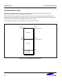
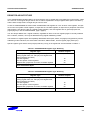
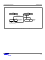
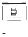
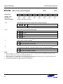
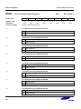
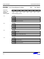
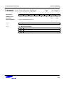
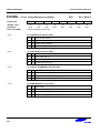
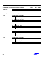
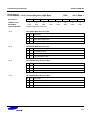
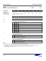
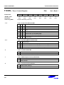
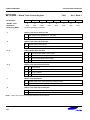
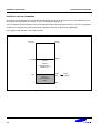
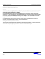
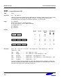
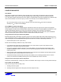
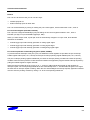
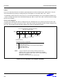
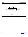
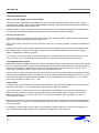
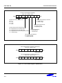
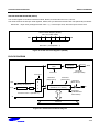
REGISTER PAGE POINTER (PP)
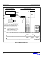
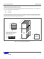
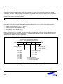
The S3C8-series architecture supports the logical expansion of the physical 256-byte internal register file (using an
8-bit data bus) into as many as 16 separately addressable register pages. Page addressing is controlled by the
register page pointer (PP, DFH). In the S3C8245/C8249 microcontroller, a paged register file expansion is
implemented for LCD data registers, and the register page pointer must be changed to address other pages.
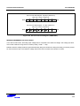
After a reset, the page pointer's source value (lower nibble) and the destination value (upper nibble) are always
"0000", automatically selecting page 0 as the source and destination page for register addressing.
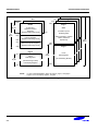
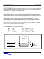
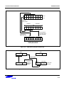
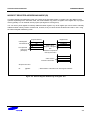
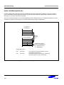
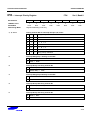
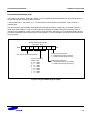
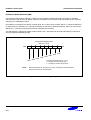
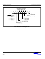
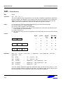
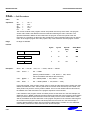
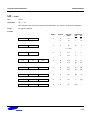
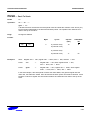
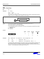
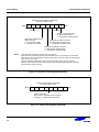
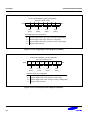
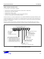
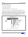
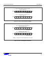
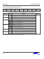
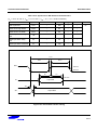
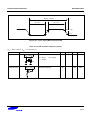
Register Page Pointer (PP)
DFH ,Set 1, R/W
MSB
.7
.6
.5
.4
.3
.2
.1
.0
LSB
Destination register page selection bits:
Source register page selection bits:
0000
0000
NOTE:
Destination: Page 0
Source: Page 0
A hardware reset operation writes the 4-bit destination and
source values shown above to the register page pointer. These values should
be modified to address other pages.
Figure 2-3. Register Page Pointer (PP)
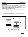
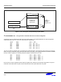
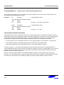
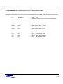
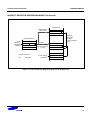
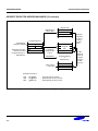
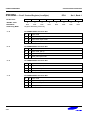
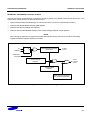
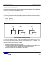
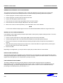
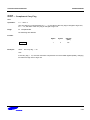
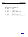
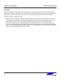
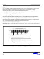
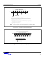
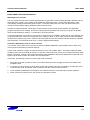
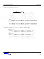
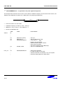
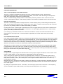
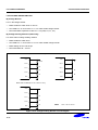
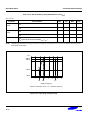
+ PROGRAMMING TIP — Using the Page Pointer for RAM clear (Page 0, Page 1)
RAMCL0
RAMCL1
NOTE:
LD
SRP
LD
CLR
DJNZ
CLR
PP,#00H
#0C0H
R0,#0FFH
@R0
R0,RAMCL0
@R0
; Destination ← 0, Source ← 0
LD
LD
CLR
DJNZ
CLR
PP,#10H
R0,#0FFH
@R0
R0,RAMCL1
@R0
; Destination ← 1, Source ← 0
; Page 1 RAM clear starts
; Page 0 RAM clear starts
; R0 = 00H
; R0 = 00H
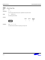
You should refer to page 6-39 and use DJNZ instruction properly when DJNZ instruction is used in your program.
2-5