1
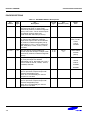
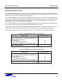
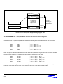
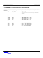
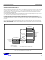
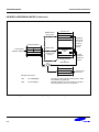
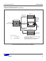
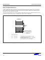
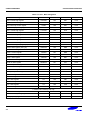
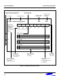
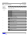
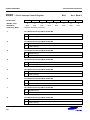
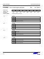
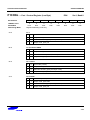
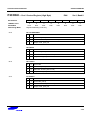
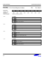
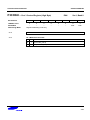
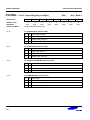
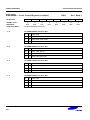
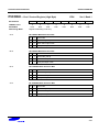
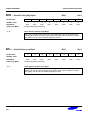
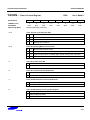
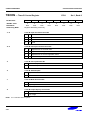
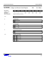
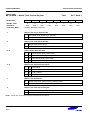
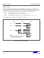
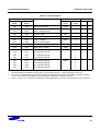
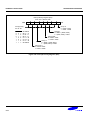
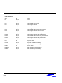
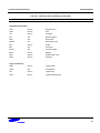
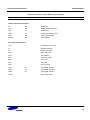
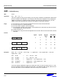
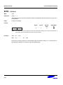
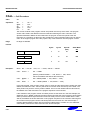
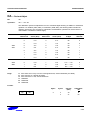
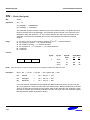
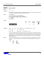
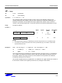
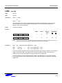
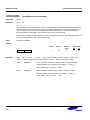
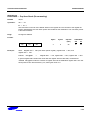
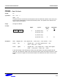
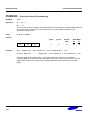
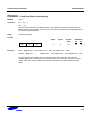
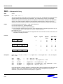
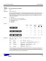
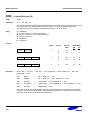
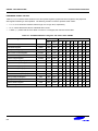
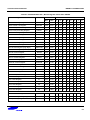
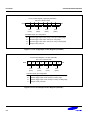
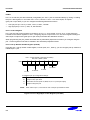
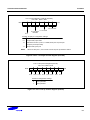
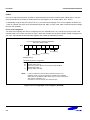
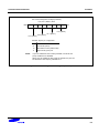
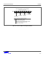
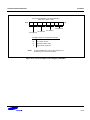
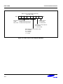
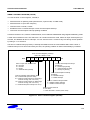
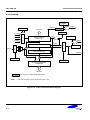
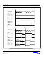
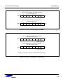
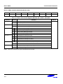
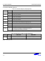
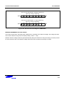
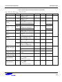
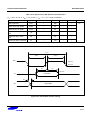
S3C8245/P8245/C8249/P8249
CONTROL REGISTER
ADCON — A/D Converter Control Register
F7H
Set 1, Bank 1
Bit Identifier
.7
.6
.5
.4
.3
.2
.1
.0
nRESET Value
–
0
0
0
0
0
0
0
Read/Write
–
R/W
R/W
R/W
R
R/W
R/W
R/W
Addressing Mode
Register addressing mode only
.7
Not used for the S3C8245/C8249
.6–.4
A/D Input Pin Selection Bits
.3
.2–.1
.0
0
0
0
ADC0
0
0
1
ADC1
0
1
0
ADC2
0
1
1
ADC3
1
0
0
ADC4
1
0
1
ADC5
1
1
0
ADC6
1
1
1
ADC7
End-of-Conversion bit (read-only)
0
Conversion not complete
1
Conversion complete
Clock Source Selection Bits
0
0
fxx/16
0
1
fxx/8
1
0
fxx/4
1
1
fxx
Start or Enable Bit
0
Disable operation
1
Start operation
4-5