1
Chapter 1: Xilinx Blockset
Down Sample
This block is listed in the following Xilinx Blockset libraries: Basic Elements and Index.
The Xilinx Down Sample block reduces the sample rate at the point where the block is
placed in your design.
The input signal is sampled at even intervals, at either the beginning (first value)
or end (last value) of a frame. The sampled value is presented on the output port
and held until the next sample is taken.
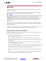
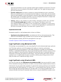
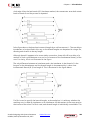
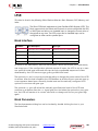
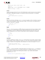
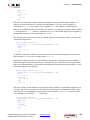
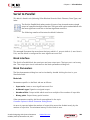
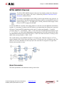
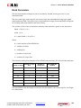
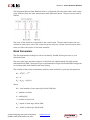
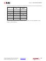
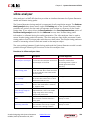
A Down Sample frame consists of l input samples, where l is sampling rate. An example
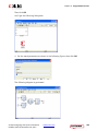
frame for a Down Sample block configured with a sampling rate of 4 is shown below.
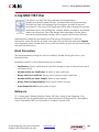
The Down Sample block is realized in hardware using one of three possible
implementations that vary in terms of implementation efficiency. The block receives two
clock enable signals in hardware, Src_CE and Dest_CE. Src_CE is the faster clock enable
signal and corresponds to the input data stream rate. Dest_CE is the slower clock enable,
corresponding to the output stream rate, for example, down sampled data. These enable
signals control the register sampling in hardware.
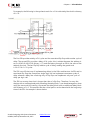
Zero Latency Down Sample
The zero latency Down Sample block must be configured to sample the first value of the
frame. The first sample in the input frame passes through the mux to the output port. A
register samples this value during the first sample duration and the mux switches to the
register output at the start of the second sample of the frame. The result is that the first
sample in a frame is present on the output port for the entire frame duration. This is the
least efficient hardware implementation as the mux introduces a combinational path from
Din to Dout. A single bit register adjusts the timing of the destination clock enable, so that
Vivado: Designing with System Generator
UG958 (v2015.4) November 18, 2015
www.xilinx.com
Send Feedback
121