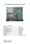
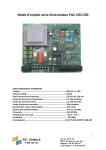
1
EX1200 SERIES SWITCH CARDS USER’S MANUAL P/N: 82-0127-001 June 23rd 2015 VTI Instruments Corp. 2031 Main Street Irvine, CA 92614-6509 (949) 955-1894 VTI Instruments Corp. TABLE OF CONTENTS INTRODUCTION Certification .......................................................................................................................................................... 6 Warranty ............................................................................................................................................................... 6 Limitation of Warranty ......................................................................................................................................... 6 Restricted Rights Legend ...................................................................................................................................... 6 Declaration of Conformity .................................................................................................................................... 6 GENERAL SAFETY INSTRUCTIONS............................................................................................................................. 7 Terms and Symbols .............................................................................................................................................. 7 Warnings............................................................................................................................................................... 7 SUPPORT RESOURCES ............................................................................................................................................... 9 SECTION 1.................................................................................................................................................................. 10 INTRODUCTION ....................................................................................................................................................... 10 Overview ............................................................................................................................................................ 10 Plug-in Module Installation ................................................................................................................................ 10 Microwave Module Installation .......................................................................................................................... 11 Module Shielding/Grounding ............................................................................................................................. 11 Scanning ............................................................................................................................................................. 11 Application Environments .................................................................................................................................. 12 SECTION 2.................................................................................................................................................................. 13 SWITCHING OVERVIEW ........................................................................................................................................... 13 General Purpose Switching................................................................................................................................. 13 Power Switching ................................................................................................................................................. 13 Matrix/Multiplexer Switching ............................................................................................................................ 13 RF Switching ...................................................................................................................................................... 14 SECTION 3.................................................................................................................................................................. 15 EX1200 SERIES TERMINAL BLOCKS ....................................................................................................................... 15 Introduction ........................................................................................................................................................ 15 Jumper Configuration ......................................................................................................................................... 16 Terminal Block Receiver .................................................................................................................................... 17 Programming Overview...................................................................................................................................... 17 Measure Thermistor Temperature ................................................................................................................. 17 Use Thermistor as a Reference Junction ....................................................................................................... 18 SECTION 4.................................................................................................................................................................. 19 EX1200-2001 PLUG-IN MODULE ........................................................................................................................... 19 20-Channel 16 Amp SPST Switch...................................................................................................................... 19 Connector Pins and Signals ................................................................................................................................ 19 Logical Diagram ................................................................................................................................................. 21 EX1200-2001 Specifications .............................................................................................................................. 22 Relay Breaking Capacity .................................................................................................................................... 22 EX1200-2002 PLUG-IN MODULE ........................................................................................................................... 23 12-Channel 16 Amp Form C (SPDT) Switch ..................................................................................................... 23 Connector Pins and Signals ................................................................................................................................ 23 Logical Diagram ................................................................................................................................................. 24 EX1200-2002 Specifications .............................................................................................................................. 25 EX1200-2007A PLUG-IN MODULE......................................................................................................................... 26 48-Channel 1000 V Multiplexer ......................................................................................................................... 26 Connector Pins and Signals ................................................................................................................................ 26 Logical Diagram ................................................................................................................................................. 28 EX1200-2007A Specifications ........................................................................................................................... 29 EX1200-2008H PLUG-IN MODULE......................................................................................................................... 30 2 EX1200 Switch Card Preface www.vtiinstruments.com 30-Channel 3 (1 x 10) High-Voltage Multiplexer .............................................................................................. 30 Connector Pins and Signals ................................................................................................................................ 30 Logical Diagram ................................................................................................................................................. 32 EX1200-2008H Specifications ........................................................................................................................... 33 EX1200-3001 PLUG-IN MODULE ........................................................................................................................... 34 1 x 64 2-wire Multiplexer ................................................................................................................................... 34 Connector Pins and Signals ................................................................................................................................ 34 Logical Diagram ................................................................................................................................................. 36 EX1200-3001 Specifications .............................................................................................................................. 38 EX1200-3001DS PLUG-IN MODULE ...................................................................................................................... 39 1 x 64 2-wire Multiplexer with Discharge Circuit .............................................................................................. 39 Connector Pins and Signals ................................................................................................................................ 39 Logical Diagram ................................................................................................................................................. 41 EX1200-3001DS Specifications ......................................................................................................................... 42 EX1200-3048 PLUG-IN MODULE ........................................................................................................................... 43 48-Channel 300 V/ 2 A Multiplexer ................................................................................................................... 43 Connector Pins and Signals ................................................................................................................................ 43 Logical Diagram ................................................................................................................................................. 45 EX1200-3048 Specifications .............................................................................................................................. 47 EX1200-3048S PLUG-IN MODULE ......................................................................................................................... 48 48-Channel Two-Wire FET Multiplexer ............................................................................................................ 48 Connector Pins and Signals ................................................................................................................................ 48 Logical Diagram ................................................................................................................................................. 50 EX1200-3048S Specifications ............................................................................................................................ 52 EX1200-3072 PLUG-IN MODULE ........................................................................................................................... 53 72-Channel 300 V/ 2 A Multiplexer ................................................................................................................... 53 Connector Pins and Signals ................................................................................................................................ 53 Logical Diagram ................................................................................................................................................. 55 EX1200-3072 Specifications .............................................................................................................................. 57 EX1200-3096 PLUG-IN MODULE ........................................................................................................................... 58 96-Channel 100 V / 0.5 A Two-Wire Multiplexer.............................................................................................. 58 Connector Pins and Signals ................................................................................................................................ 58 Logical Diagram ................................................................................................................................................. 61 EX1200-3096 Specifications .............................................................................................................................. 63 EX1200-3164 PLUG-IN MODULE ........................................................................................................................... 64 16 (1x4) 2-wire 300 V/ 2 Amp Multiplexer ........................................................................................................ 64 Connector Pins and Signals ................................................................................................................................ 64 Logical Diagram ................................................................................................................................................. 66 EX1200-3164 Specifications .............................................................................................................................. 68 EX1200-3824 PLUG-IN MODULE ........................................................................................................................... 69 8 (1 x 24) Solid State, 100V/100mA Multiplexer ............................................................................................... 69 EX1200-3824 Standard Board ............................................................................................................................ 69 EX1200-3824 with Attenuator Option................................................................................................................ 69 Connector Pins and Signals ................................................................................................................................ 70 Logical Diagram ................................................................................................................................................. 72 EX1200-38TB .................................................................................................................................................... 73 EX1200-3824 Specifications .............................................................................................................................. 76 EX1200-4003 PLUG-IN MODULE ........................................................................................................................... 77 Dual 4 x 16 Two-Wire Matrix, 300 V / 2 A ....................................................................................................... 77 Logical Diagram ................................................................................................................................................. 79 EX1200-4003 Specifications .............................................................................................................................. 81 EX1200-4128 PLUG-IN MODULE ........................................................................................................................... 82 4 x 128 One-wire Matrix, 150 V/0.5 A............................................................................................................... 82 Connector Pins and Signals ................................................................................................................................ 82 Logical Diagram ................................................................................................................................................. 86 EX1200-4128 Specifications .............................................................................................................................. 88 EX1200-4260 PLUG-IN MODULE ........................................................................................................................... 89 EX1200 Switch Card Preface 3 VTI Instruments Corp. 2 x 60 2-Wire Matrix .......................................................................................................................................... 89 Connector Pins and Signals ................................................................................................................................ 89 Logical Diagram ................................................................................................................................................. 93 EX1200-4260 Specifications .............................................................................................................................. 94 Relay Breaking Capacity .................................................................................................................................... 94 EX1200-4264 PLUG-IN MODULE ........................................................................................................................... 95 2 x 64 2-Wire Matrix .......................................................................................................................................... 95 Connector Pins and Signals ................................................................................................................................ 95 Logical Diagram ................................................................................................................................................. 99 EX1200-4264 Specifications ............................................................................................................................ 100 Relay Breaking Capacity .................................................................................................................................. 100 EX1200-5001 PLUG-IN MODULE ......................................................................................................................... 101 80-Channel 2 Amp Form A (SPST) Switch ..................................................................................................... 101 Connector Pins and Signals .............................................................................................................................. 101 Logical Diagram ............................................................................................................................................... 103 EX1200-5001 Specifications ............................................................................................................................ 105 EX1200-5002 PLUG-IN MODULE ......................................................................................................................... 106 32-Channel, 2 Amp Form C (SPDT) Switch .................................................................................................... 106 Connector Pins and Signals .............................................................................................................................. 106 Logical Diagram ............................................................................................................................................... 108 EX1200-5002 Specifications ............................................................................................................................ 110 EX1200-5004 PLUG-IN MODULE ......................................................................................................................... 111 32-Channel, 5 A SPDT Switch ......................................................................................................................... 111 Connector Pins and Signals .............................................................................................................................. 111 Logical Diagram ............................................................................................................................................... 113 EX1200-5004 Specifications ............................................................................................................................ 114 378HEX1200-5006 PLUG-IN MODULE ................................................................................................................. 115 40-Channel 2 Amp Form A (SPST) Switch ..................................................................................................... 115 Connector Pins and Signals .............................................................................................................................. 115 Logical Diagram ............................................................................................................................................... 117 EX1200-5006 Specifications ............................................................................................................................ 119 EX1200-6101 PLUG-IN MODULE ......................................................................................................................... 120 10 SP4T RF Multiplexers, 1.3 GHz .................................................................................................................. 120 Connector Pins and Signals .............................................................................................................................. 120 Logical Diagram ............................................................................................................................................... 122 EX1200-6101 Specifications ............................................................................................................................ 123 EX1200-6102 PLUG-IN MODULE ......................................................................................................................... 124 17-Channel (1x2) Coaxial Switches, 1.3GHz ................................................................................................... 124 Connector Pins and Signals .............................................................................................................................. 124 Logical Diagram ............................................................................................................................................... 126 EX1200-6102 Specifications ............................................................................................................................ 127 EX1200-6111 PLUG-IN MODULE ......................................................................................................................... 128 5-Channel SP4T Coaxial Switch ...................................................................................................................... 128 Connector Pins and Signals .............................................................................................................................. 128 Logical Diagram ............................................................................................................................................... 130 EX1200-6111 Specifications ............................................................................................................................ 131 EX1200-6216 PLUG-IN MODULE ......................................................................................................................... 132 Dual 1 x 16 RF Mux, 1 GHz Switch................................................................................................................. 132 Connector Pins and Signals .............................................................................................................................. 132 Logical Diagram ............................................................................................................................................... 134 EX1200-6216 Specifications ............................................................................................................................ 135 EX1200-6216HV PLUG-IN MODULE .................................................................................................................... 136 Dual (1x16) 500 V 250 MHz Multiplexers....................................................................................................... 136 Connector Pins and Signals .............................................................................................................................. 136 Logical Diagram ............................................................................................................................................... 138 EX1200-6216HV Specifications ...................................................................................................................... 139 EX1200-6301 PLUG-IN MODULE ......................................................................................................................... 140 4 EX1200 Switch Card Preface www.vtiinstruments.com 4 Channel SP4T, RF Multiplexer, 50 Ω, 3 GHz ............................................................................................. 140 Connector Pins and Signals .............................................................................................................................. 140 Logical Diagram ............................................................................................................................................... 141 EX1200-6301 Specifications ............................................................................................................................ 142 EX1200-6301T PLUG-IN MODULE ....................................................................................................................... 143 4 Channel SP4T, Self-terminated RF Multiplexer, 50 Ω, 3 GHz ................................................................... 143 Connector Pins and Signals .............................................................................................................................. 143 Logical Diagram ............................................................................................................................................... 144 EX1200-6301T Specifications .......................................................................................................................... 145 EX1200-7100 PLUG-IN MODULE ......................................................................................................................... 146 DC - 26 GHz Microwave Switch Carrier and Relay Driver ............................................................................. 146 Front Panel Enclosure ....................................................................................................................................... 146 Microwave Switch Modules ............................................................................................................................. 147 7102 Microwave Module ............................................................................................................................ 147 7104 Microwave Module ............................................................................................................................ 148 7106 Microwave Module ............................................................................................................................ 148 7122 Microwave Module ............................................................................................................................ 149 Installing a Switch Module .......................................................................................................................... 149 EX1200-7100 Carrier Front Panel Connectors ................................................................................................. 150 EX1200-7100 Soft Front Panel......................................................................................................................... 150 EX1200-7100 Specifications ............................................................................................................................ 152 APPENDIX A............................................................................................................................................................. 153 POWER CONSUMPTION AND WEIGHT .................................................................................................................... 153 Reference Tables .............................................................................................................................................. 153 APPENDIX B ............................................................................................................................................................. 155 SWITCH CARD ACCESSORIES ................................................................................................................................ 155 List of Accessories............................................................................................................................................ 155 26-pin Connector ......................................................................................................................................... 155 41-pin Connector ......................................................................................................................................... 156 104-pin Connector ....................................................................................................................................... 156 160-pin Connector ....................................................................................................................................... 157 200-pin Connector ....................................................................................................................................... 157 50-pin Connector ......................................................................................................................................... 157 EX1200 Switch Card Preface 5 VTI Instruments Corp. CERTIFICATION VTI Instruments Corp. (VTI) certifies that this product met its published specifications at the time of shipment from the factory. VTI further certifies that its calibration measurements are traceable to the United States National Institute of Standards and Technology (formerly National Bureau of Standards), to the extent allowed by that organization’s calibration facility, and to the calibration facilities of other International Standards Organization members. Note that the contents of this document are subject to change without notice. WARRANTY The product referred to herein is warranted against defects in material and workmanship for a period of one year from the receipt date of the product at customer’s facility. The sole and exclusive remedy for breach of any warranty concerning these goods shall be repair or replacement of defective parts, or a refund of the purchase price, to be determined at the option of VTI. For warranty service or repair, this product must be returned to a VTI Instruments authorized service center. The product shall be shipped prepaid to VTI and VTI shall prepay all returns of the product to the buyer. However, the buyer shall pay all shipping charges, duties, and taxes for products returned to VTI from another country. VTI warrants that its software and firmware designated by VTI for use with a product will executeits programming when properly installed on that product. VTI does not however warrant that the operation of the product, or software, or firmware will be uninterrupted or error free. LIMITATION OF WARRANTY The warranty shall not apply to defects resulting from improper or inadequate maintenance by the buyer, buyersupplied products or interfacing, unauthorized modification or misuse, operation outside the environmental specifications for the product, or improper site preparation or maintenance. VTI Instruments Corp. shall not be liable for injury to property other than the goods themselves. Other than the limited warranty stated above, VTI Instruments Corp. makes no other warranties, express, or implied, with respect to the quality of product beyond the description of the goods on the face of the contract. VTI specifically disclaims the implied warranties of merchantability and fitness for a particular purpose. RESTRICTED RIGHTS LEGEND Use, duplication, or disclosure by the Government is subject to restrictions as set forth in subdivision (b)(3)(ii) of the Rights in Technical Data and Computer Software clause in DFARS 252.227-7013. DECLARATION OF CONFORMITY The declaration of conformity for the EX1200 Series Mainframe applies to all of its available plug-in modules and options. For specifics, refer to the EX1200 Series Mainframe User’s Manual. VTI Instruments Corp. 2031 Main Street Irvine, CA 92614-6509 U.S.A. 6 EX1200 Switch Card Preface www.vtiinstruments.com GENERAL SAFETY INSTRUCTIONS Review the following safety precautions to avoid bodily injury and/or damage to the product. These precautions must be observed during all phases of operation or service of this product. Failure to comply with these precautions, or with specific warnings elsewhere in this manual, violates safety standards of design, manufacture, and intended use of the product. Service should only be performed by qualified personnel. TERMS AND SYMBOLS These terms may appear in this manual: WARNING Indicates that a procedure or condition may cause bodily injury or death. CAUTION Indicates that a procedure or condition could possibly cause damage to equipment or loss of data. These symbols may appear on the product: ATTENTION - Important safety instructions Frame or chassis ground Indicates that the product was manufactured after August 13, 2005. This mark is placed in accordance with EN 50419, Marking of electrical and electronic equipment in accordance with Article 11(2) of Directive 2002/96/EC (WEEE). End-of-life product can be returned to VTI by obtaining an RMA number. Fees for take_2ack and recycling will apply if not prohibited by national law. WARNINGS Follow these precautions to avoid injury or damage to the product: Use Proper Power Cord The power cable provided with this instrument meets the required regulatory and statutory safety standards as indicated by this product’s declaration of conformity. VTI recommends that the power cord provided be used with the instrument that it is provided with. If a different power cord is must to be used, however, it is the responsibility of the user to select a power cord that meets any and all regulatory and statutory requirements for their industry and country. Use Proper Power Source To avoid electrical overload, electric shock, or fire hazard, do not use a power source that applies other than the specified voltage. Prior to using the EX1200 series switch cards, it is imperative that the power consumption of all cards that will be installed in the mainframe be calculated on all power supply rails. Power consumption information is provided in Appendix A. Information regarding power consumption calculations can be found in the EX1200 Series User’s Manual (P/N: 82-0127-000). Failure to do so may result in damaging the switch card and the mainframe. Power Consumption EX1200 Switch Card Preface 7 VTI Instruments Corp. WARNINGS (CONT.) Avoid Electric Shock To avoid electric shock or fire hazard, do not operate this product with the covers removed. Do not connect or disconnect any cable, probes, test leads, etc. while they are connected to a voltage source. Remove all power and unplug unit before performing any service. Service should only be performed by qualified personnel. Ground the Product This product is grounded through the grounding conductor of the power cord. To avoid electric shock, the grounding conductor must be connected to earth ground. Operating Conditions To avoid injury, electric shock or fire hazard: Do not operate in wet or damp conditions. Do not operate in an explosive atmosphere. Operate or store only in specified temperature range. Provide proper clearance for product ventilation to prevent overheating. DO NOT operate if any damage to this product is suspected. Product should be inspected or serviced only by qualified personnel. The operator of this instrument is advised that if the equipment is used in a manner not specified in this manual, the protection provided by the equipment may be impaired. Conformity is checked by inspection. Improper Use 8 EX1200 Switch Card Preface www.vtiinstruments.com SUPPORT RESOURCES Support resources for this product are available on the Internet and at VTI Instruments customer support centers. VTI Instruments Corp. World Headquarters VTI Instruments Corp. 2031 Main Street Irvine, CA 92614-6509 Phone: (949) 955-1894 Fax: (949) 955-3041 VTI Instruments Cleveland Instrument Division 5425 Warner Road Suite 13 Valley View, OH 44125 Phone: (216) 447-8950 Fax: (216) 447-8951 VTI Instruments Lake Stevens Instrument Division 3216 Wetmore Avenue, Suite 1 Everett, WA 98201 Phone: (949) 955-1894 Fax: (949) 955-3041 VTI Instruments, Pvt. Ltd. Bangalore Instrument Division 74, 75, Millers Road Bangalore – 560 052 India Phone: +91 80 4040 7900 Phone: +91 80 4162 0200 Fax: +91 80 4170 0200 Technical Support Phone: (949) 955-1894 Fax: (949) 955-3041 E-mail: [email protected] 159H Visit http://www.vtiinstruments.com for worldwide support sites and service plan information. 160H EX1200 Switch Card Preface 9 VTI Instruments Corp. 321H SECTION 1 INTRODUCTION OVERVIEW Signal switching is at the heart of every automated test system. It is responsible for routing signals of interest between test system instruments and the device under test (DUT). The purpose of the testing is to improve product quality. The switch distributes instrument I/O, which can reduce overall system cost. Since switching is effectively an extension of the instrument, it should be transparent to the overall system. EX1200 switching products employ extensive signal shielding and high-quality relays to ensure that the test system is “minimally aware” of the switch’s presence. PLUG-IN MODULE INSTALLATION All EX1200 series switch cards must be installed into an EX1200 series mainframe to be used. The mainframe operates on 90 V to 250 V at 50 Hz/60 Hz which is used to supply the cards the dc voltages required for the cards to function properly. Before installing a plug-in module into an EX1200 series mainframe, make sure that the mainframe is powered down. Insert the module into the base unit by orienting the module so that the circuit board of the module can be inserted into the slot of the base unit. Position the cover so that it fits into the module’s slot groove. Once the module is properly aligned, push the module back and firmly insert it into the backplane connector. FIGURE 1-1: MODULE INSTALLATION (EX1200-3048 SHOWN) NOTE 10 To maximize air flow for cooling, blanking panels (P/N: 41-0472-012) should be installed into the empty slots of EX1200 mainframes. EX1200 Switch Card Introduction www.vtiinstruments.com The maximum safe voltage for an EX1200 system is determined by the plug-in card with the lowest voltage rating. MICROWAVE MODULE INSTALLATION For the EX1200-7100 Plug-in Module, microwave switch modules can be installed. Before installing a switch module into the EX1200-7100 carrier, ensure that the mainframe is powered down. Insert the switch module into the desired slot of the carrier. Slide the module into the mating connector at the rear of the carrier using the two guide pins to ensure proper orientation. Once the guide pins are aligned, push the module firmly mating connector. The module is then sMUXred to the front panel of the carrier using four socket head cap screws. FIGURE 1-2: MICROWAVE SWITCH INSTALLATION MODULE SHIELDING/GROUNDING Most EX1200 modules incorporate an integral shield into the design of the PCB that attenuates noise and crosstalk between adjacent channels/modules. To properly utilize this feature, tie the appropriate front panel connector pins to the mating cable’s common shield and/or ground. If this feature is present on a module, the pins are identified in the module appendix in the Connector Pins and Signals table and the signal is noted as “SHIELD”. Leaving the SHIELD pins unconnected may have detrimental effects on signal crosstalk and isolation. If no cable shield connection is available, chassis ground may be used to attach the SHIELD pins. Many plug-in modules also incorporate ground pins, labeled “GND_C” or simply “GND”. These pins tie the module to chassis ground. Note that the SHIELD pins are not tied to ground and have no electrical connections. SCANNING The EX1200 switch cards provide scanlist functionality to maximize measurement throughput. The scanlist allows the relay state to be advanced by a hardware trigger rather than requiring the state of the relay to be updated manually during program execution. Doing this eliminates the need to wait on the controller to wait for a state to be settled and send the command to update relays providing maximum throughput performance EX1200 Switch Card Introduction 11 VTI Instruments Corp. APPLICATION ENVIRONMENTS The EX1200 switching platform supports a wide variety of application environments. The switches can be manually controlled through the embedded, web-based soft front panel or programmatically on a Windows-based PC through the provided IVI VTEXSwitch driver controlled on most platforms through the C++ driver. The EX1200 also allows for integration into NI’s Switch Executive for high-level configuration and control. 12 EX1200 Switch Card Introduction www.vtiinstruments.com 322H SECTION 2 SWITCHING OVERVIEW GENERAL PURPOSE SWITCHING When selecting switch cards for a test system, the following should be taken into consideration: Power Specifications Minimum Contact Rating Switching Time Bandwidth The relay must be able to accommodate both the voltage, current, and total power that will be switched and all of these specifications should be checked before making a selection. The minimum contact rating and switching time specifications are important in systems where relays will be opened and closed many times throughout the test. The faster the switch performs, the faster the test will finish. The bandwidth specification indicates the frequencies the switch is able to switch. Interchannel isolation and crosstalk are also affected by the frequency of the signals being switched. POWER SWITCHING The EX1200-200x high-power switch cards provide high-power switching in a small form factor. The EX1200-2001 and the EX1200-2002 are the only switch modules in their class with the ability to switch up to 16 A. As such, the high-power cards are an ideal solution for applications such as: ac line power switching, switching of dc or power supplies, controlling or driving relays for industrial machines (robotics, numerical control machines), automotive engine control, and solenoid switching. These switch cards also include a front panel interrupt line which will open all relays in the module to provide safety. They can also be used in the setup phase of a scanlist to switch power to and from a DUT before reading data into a multiplexer to the DMM. MATRIX/MULTIPLEXER SWITCHING Matrix and multiplexer cards allow the user the ability to combine multiple in the same chassis to create larger switching systems: For matrix cards, multiple cards can be combined by connecting either rows or columns of the relay together. For example, by placing six EX1200-4128’s in a chassis and connecting all four rows of each module to the EX1200 backplane, a 4 x 768 can be formed is a 1U rack with no external wiring. To improve bandwidth specifications, it is important to utilize the stub breaking relays that are incorporated into most matrix and multiplexer cards. These relays typically separate banks of relays from each other or isolate the switch card from the DMM backplane. By keeping these relays open, the length a signal must travel, and the amount of resistance it will encounter, can be reduced, increasing the path’s bandwidth. Examples of these relays are shown in Figure 2-1. 323H EX1200 Switching Overview 13 VTI Instruments Corp. CH5_6L (Pin C20) K39 CH6_6L (Pin C24) K47 CH5_7H (Pin D19) K40 K48 CH5_8H (Pin E19) K80 CH6_7H (Pin D23) CH1_COMH (Pin B1) CH6_7L (Pin D24) CH1_COML (Pin B2) CH6_8H (Pin E23) CH5_8L (Pin E20) CH6_8L (Pin E24) K77 K78 CH5_COMH (Pin B17) CH6_COMH (Pin B21) CH5_COML (Pin B18) CH6_COML (Pin B22) K84 DMM Bus CH5_7L (Pin D20) CH5_COMH (Pin B17) BPL_HI CH5_COML (Pin B18) BPL_LO Stub Breaking Relays (from EX1200-3001) FIGURE 2-1: STUB BREAKING RELAYS When programming switches to perform 2-wire and 4-wire measurements, the 2-wire and 4-wire channel names must be used. For “standard” matrix cards (i.e. 2-banks of paired H/L inputs), the 2- and 4-wire name, the 1-wire names is used as the base. The convention is illustrated in Table 2-1 below: 324H 1-Wire Channel Name CH1_1L CH1_1H CH2_1L CH2_1H CH1_2L CH1_2H CH2_2L CH2_2H 2-Wire Channel Name 4-Wire Channel Name CH1_1 CH_1 CH2_1 CH1_2 CH_2 CH2_2 TABLE 2-1: STANDARD 2- AND 4-WIRE NAMING CONVENTIONS For “non-standard” matrix cards, this convention cannot be used, however. For these switch cards, the full 2- and 4-wire names are provided following the 1-wire discussion for those cards. RF SWITCHING The EX1200-6xxx cards can be used for high bandwidth applications such as switching to/from oscilloscopes and function generators. These modules provide a maximum of 10 W of switching power and the stub effects are terminated to ensure maximum signal fidelity. 14 EX1200 Switching Overview www.vtiinstruments.com 325H SECTION 3 EX1200 SERIES TERMINAL BLOCKS INTRODUCTION VTI offers differential and single-ended terminal blocks (TBs) for many of the EX1200 series switch cards. The terminal blocks can be used to simplify cabling. In addition to this, the differential terminal blocks also provide users an on-board thermistor for cold junction compensation (CJC) when making temperature measurements. Signal pin mapping is provided for the terminal blocks with its associated switch card. FIGURE 3-1: EX1200-TB200 EX1200 Series Terminal Blocks 15 VTI Instruments Corp. JUMPER CONFIGURATION Differential TBs have the ability to use an on-board 10 kΩ thermistor (RT1) to connect to an instrument when temperature measurements are being made. Before doing so, the P2 header must be configured correctly. The function of this header is to make a connection between the T1 and T2 terminals on the terminal block, the CJC (RT1) sensor, and two other TB terminals. In the default position, pin 1 is shorted to pin 6 and pins 3 and 4 are shorted (see Figure 3-2) on P2. This configuration allows T1 and T2 to be used in any type of measurement. When configured to one of the other two configurations, the channels associated with these terminals are dedicated to making temperature measurements and cannot be used in any other manner. 326H To use RT1 for CJC measurements, short pin 2 to pin 3 and pin 4 to pin 5. This will join T1 and T2 to L_VS and H_VS. The terminal numbers for L_VS and H_VS differ between TB modules and are documented with the terminal block pin mapping information for each switch card. To use an external sensor for temperature measurements, short pin 1 to pin 2 and pins 5 and 6 on P2. This joins T1 and T2 to RL_I and RH_I. For the TB104 and TB160, the external sensor should be connected to T1 and T2 or T161 and T162 when in this configuration. For the TB200, the external sensor can be connected T1 and T2 or T181 and T182 when in this configuration. FIGURE 3-2: P2 JUMPER CONFIGURATION DIAGRAM NOTE The actual switch card channel that is dedicated to temperature measurement through the P2 header is dependent on the channel to which T1 and T2 of the terminal block are connected. Figure 3-2, an EX1200-TB160-1 is shown where T1 and T2 are connected to CH1_1L and CH1_1H, respectively. The channels are indicated in the Terminal Block Pin Mapping discussion for each switch card. 327H 16 EX1200 Series Terminal Blocks www.vtiinstruments.com TERMINAL BLOCK RECEIVER The EX1200-TBR chassis is a 1U receiver capable of housing six terminal blocks. The EX1200-TBR ships with rubber feet for table top installations, but may be fitted with rackmount ears for installation into a test rack (P/N: 70-0367-010). To install a terminal block into the EX1200-TBR, insert the flanges on the side of the terminal block into the guide rails of the desired slot. Continue to push the terminal block into the receiver until it is sMUXred by the rear-locking latch of the receiver. To remove the terminal block from the EX1200-TBR, hold the center thumbscrew on the terminal block, then pull the terminal block from the receiver. Rear-locking latch Terminal Block Flange Cabling removed for clarity FIGURE 3-3: TERMINAL BLOCK INSTALLATION INTO THE EX1200-TBR PROGRAMMING OVERVIEW To measure the thermistor temperature, first ensure that the P2 jumper has been configured properly (see Jumper Configuration for more detail). Next, a scan list is developed which scans CH1_1. In the following programming overview, a method for taking measurements using the onboard thermistor will be provided. 328H Two scenarios will be provided: one where only the thermistor temperature is measured and one where the RT1 is used as a reference junction and other channels make temperature measurements. In the first example, the user can only measure the thermistor temperature at CH1_1. In the second example, the user can measure the thermistor temperature at CH1_1 and can also measure temperature on another channel which uses the CH1_1 as a reference junction. Note that, in these examples, it is assumed that the EX1200 DMM is being used and that the P2 jumper has been configured appropriately. Measure Thermistor Temperature Either the VTEXScanner driver or the scanner soft front panel can be used to perform this sequence. 1) Set the DMM to measure temperature using the thermistor. a. Set the DMM function to Temperature. b. Set the transducer type to Thermistor. c. Set the thermistor resistance to 10000 (the thermistor is 10 kΩ). EX1200 Series Terminal Blocks 17 VTI Instruments Corp. 2) Save and provide a name for the DMM configuration for the scanning purposes (here, TEMP is used). 3) Setup the scanlist a. Add a scan step with a sweep phase that scans CH1_1 using the previously saved configuration (e.g. CH1_1=TEMP) b. The setup phase can be ignored for this example. 4) Initiate & Read a. Initiate the scan b. Read back the data Use Thermistor as a Reference Junction 1) Set the DMM to measure temperature using the thermistor. a. Set the DMM function to Temperature. b. Set the transducer type to Thermistor. c. Set the thermistor resistance to 10000 (the thermistor is 10 kΩ). d. Set the isReferenceJunction parameter to True. 2) Save and provide a name for the DMM configuration for the scanning purposes. 3) Set the DMM to measure temperature using a Type K thermocouple (any thermocouple type can be selected here, but Type K below). a. Set the DMM function to Temperature. b. Set the transducer type to Thermocouple. c. Set the thermocouple type to Type K. d. Set the reference type to External. e. Set the isReferenceJunction parameter to False. 4) Save and provide a name for the DMM configuration for the scanning purposes. 5) Setup the scanlist a. Add a scan step with a sweep phase that scans CH1_1 using the first saved configuration. (e.g. CH1_1=RefJunction). b. Add another scan step with a sweep phase that scans another channel (e.g. CH1_2=TEMP). c. The setup phase can be ignored for this example. 6) Initiate & Read a. Initiate the scan b. Read back the data 18 EX1200 Series Terminal Blocks www.vtiinstruments.com 329H SECTION 4 EX1200-2001 PLUG-IN MODULE 20-CHANNEL 16 AMP SPST SWITCH The EX1200-2001 and EX1200-2002 are the only switch modules in their class with the ability to switch up to 16 A. Some applications include: ac line power switching, switching of dc or ac power supplies, control or driving relays for industrial machines (robotics, numerical control machines), automotive engine control, and solenoid switching. Since these modules typically switch power to the UUT or interface, the digital input lines on the EX1200 series mainframes support the ability to force all relays automatically to their normally open state if a fault condition occurs. This approach instantly removes all power to the UUT or interface. These modules can be automatically configured in the setup phase at the beginning of each scan step to facilitate test sequencing and control. The EX1200-2001 can be controlled programmatically using IviSwtch-compliant calls. Both path level programming and individual relay control are available. Refer to the host driver documentation for additional details. Figure 4-2 provides a logical diagram of the switch module and identifies the switches used by the module. This information can be used for individual relay control through the driver. 330H CONNECTOR PINS AND SIGNALS FIGURE 4-1: EX1200-2001 FRONT PANEL (FRONT VIEW) EX1200-2001 Plug-in Module 19 VTI Instruments Corp. NOTE Pin Signal Pin Signal A B C D E F H J K L M N P R S T U V W X Y CH_1NO CH_1COM CH_2NO CH_2COM CH_3NO CH_3COM CH_4NO CH_4COM CH_5NO CH_5COM CH_6NO CH_6COM CH_7NO CH_7COM CH_8NO CH_8COM CH_9NO CH_9COM CH_10NO CH_10COM CH_11NO Z a b c d e f h j k m n p r s t u v w x CH_11COM CH_12NO CH_12COM CH_13NO CH_13COM CH_14NO CH_14COM CH_15NO CH_15COM CH_16NO CH_16COM CH_17NO CH_17COM CH_18NO CH_18COM CH_19NO CH_19COM CH_20NO CH_20COM SHIELD Pin x is connected to a shield layer located directly under the relays and connecting wires. Optimum performance is obtained when Pin x is tied to system or chassis ground and the front panel mounting screws are sMUXred to the chassis frame. TABLE 4-1: CONNECTOR PINS & SIGNAL ASSIGNMENTS 20 EX1200-2001 Plug-in Module www.vtiinstruments.com LOGICAL DIAGRAM CH_1COM (Pin B) CH_1NO (Pin A) CH_11COM (Pin Z) CH_2COM (Pin D) CH_2NO (Pin C) CH_12COM (Pin b) CH_3NO (Pin E) CH_13COM (Pin d) CH_4NO (Pin H) CH_14COM (Pin f) CH_5NO (Pin K) CH_15COM (Pin j) CH_6NO (Pin M) CH_16COM (Pin m) CH_7NO (Pin P) CH_17COM (Pin p) CH_8NO (Pin S) CH_18COM (Pin s) CH_9NO (Pin U) CH_19COM (Pin u) CH_19NO (Pin t) K19 K9 CH_10COM (Pin X) CH_18NO (Pin r) K18 K8 CH_9COM (Pin V) CH_17NO (Pin n) K17 K7 CH_8COM (Pin T) CH_16NO (Pin k) K16 K6 CH_7COM (Pin R) CH_15NO (Pin h) K15 K5 CH_6COM (Pin N) CH_14NO (Pin e) K14 K4 CH_5COM (Pin L) CH_13NO (Pin c) K13 K3 CH_4COM (Pin J) CH_12NO (Pin a) K12 K2 CH_3COM (Pin F) CH_11NO (Pin Y) K11 K1 CH_10NO (Pin W) CH_20COM (Pin w) CH_20NO (Pin v) K20 K10 FIGURE 4-2: EX1200-2001 LOGICAL DIAGRAM EX1200-2001 Plug-in Module 21 VTI Instruments Corp. EX1200-2001 SPECIFICATIONS GENERAL SPECIFICATIONS CHANNEL COUNT 20 SPST RELAY TYPE Electromechanical, fail-safe MAXIMUM SWITCHING VOLTAGE 250 V ac rms, 125 V dc MAXIMUM SWITCHING CURRENT 16 A MAXIMUM SWITCHING POWER 480 W dc, 2000 VA per channel (see the Figure 4-3 for more information) 331H MINIMUM CONTACT RATING* 12 V dc, 0.1 A *This value is in reference to a resistive load. Minimum capacity changes depending on switching frequency and environmental conditions RATED SWITCH OPERATIONS Mechanical Electrical SWITCHING TIME 5 x 10⁷ 1 x 10⁵ at full load < 10 ms PATH RESISTANCE < 100 mΩ INSULATION RESISTANCE >1x10⁹ Ω MAXIMUM THERMAL OFFSET PER CHANNEL (HI-LO) < 50 μV CAPACITANCE <20 pF Open channel <75 pF Channel-mainframe BANDWIDTH (-3 dB) 40 MHz (typical) INSERTION LOSS (TYPICAL) < 0.2 dB 100 kHz < 0.5 dB 1 MHz < 1.0 dB 10 MHz CROSSTALK (TYPICAL) < -48 dB 100 kHz < -33 dB 1 MHz < -19 dB 10 MHz For mating connector, crimp pins, and other accessories, please refer to Appendix B. RELAY BREAKING CAPACITY FIGURE 4-3: RELAY BREAKING CAPACITY 22 EX1200-2001 Plug-in Module www.vtiinstruments.com EX1200-2002 PLUG-IN MODULE 12-CHANNEL 16 AMP FORM C (SPDT) SWITCH The EX1200-2001 and EX1200-2002 are the only switch modules in their class with the ability to switch up to 16 A. Some applications include: ac line power switching, switching of dc or ac power supplies, control or driving relays for industrial machines (robotics, numerical control machines), automotive engine control, and solenoid switching. Since these modules typically switch power to the UUT or interface, the digital input lines on the EX1200 series mainframes support the ability to force all relays automatically to their normally open state if a fault condition occurs. This approach instantly removes all power to the UUT or interface. These modules can be automatically configured in the setup phase at the beginning of each scan step to facilitate test sequencing and control. The EX1200-2002 can be controlled programmatically using IviSwtch-compliant calls. Both path level programming and individual relay control are available. Refer to the host driver documentation for additional details. Figure 4-5 provides a logical diagram of the switch module and identifies the switches used by the module. This information can be used for individual relay control through the driver. 333H CONNECTOR PINS AND SIGNALS FIGURE 4-4: EX1200-2002 FRONT PANEL (FRONT VIEW) EX1200-2002 Plug-in Module 23 VTI Instruments Corp. Pin A B C D E F H J K L M N P R S T U V W X Y NOTE Signal CH_1NO CH_1COM CH_1NC CH_2NO CH_2COM CH_2NC CH_3NO CH_3COM CH_3NC CH_4NO CH_4COM CH_4NC CH_5NO CH_5COM CH_5NC CH_6NO CH_6COM CH_6NC CH_7NO CH_7COM CH_7NC Pin Z a b c d e f h j k m n p r s t u v w x Signal CH_8NO CH_8COM CH_8NC CH_9NO CH_9COM CH_9NC CH_10NO CH_10COM CH_10NC CH_11NO CH_11COM CH_11NC CH_12NO CH_12COM CH_12NC UNUSED UNUSED UNUSED UNUSED SHIELD Pin x is connected to a shield layer located directly under the relays and connecting wires. Optimum performance is obtained when Pin x is tied to system or chassis ground and the front panel mounting screws are sMUXred to the chassis frame. TABLE 4-2: CONNECTOR PINS & SIGNAL ASSIGNMENTS LOGICAL DIAGRAM CH_7NC (Pin Y) CH_1NC (Pin C) CH_7COM (Pin X) CH_1COM (Pin B) K1 CH_1NO (Pin A) CH_7NO (Pin W) K7 CH_8NC (Pin b) CH_2NC (Pin F) CH_8COM (Pin a) CH_2COM (Pin E) K2 CH_2NO (Pin D) CH_8NO (Pin Z) K8 CH_9NC (Pin e) CH_3NC (Pin K) CH_9COM (Pin d) CH_3COM (Pin J) K3 CH_3NO (Pin H) CH_9NO (Pin c) K9 CH_10NC (Pin j) CH_4NC (Pin N) CH_10COM (Pin h) CH_4COM (Pin M) K4 CH_4NO (Pin L) K10 CH_10NO (Pin f) CH_11NC (Pin n) CH_5NC (Pin S) CH_11COM (Pin m) CH_5COM (Pin R) K5 CH_5NO (Pin P) K11 CH_11NO (Pin k) CH_12NC (Pin s) CH_6NC (Pin V) CH_12COM (Pin r) CH_6COM (Pin U) K6 CH_6NO (Pin T) K12 CH_12NO (Pin p) FIGURE 4-5: EX1200-2002 LOGICAL DIAGRAM 24 EX1200-2002 Plug-in Module www.vtiinstruments.com EX1200-2002 SPECIFICATIONS GENERAL SPECIFICATIONS CHANNEL COUNT 12 SPDT RELAY TYPE Electromechanical, fail-safe MAXIMUM SWITCHING VOLTAGE 250 V ac rms, 125 V dc MAXIMUM SWITCHING CURRENT 16 A MAXIMUM SWITCHING POWER 480 W dc, 2000 VA per channel MINIMUM CONTACT RATING* 12 V dc, 0.1 A *This value is in reference to a resistive load. Minimum capacity changes depending on switching frequency and environmental conditions RATED SWITCH OPERATIONS Mechanical Electrical SWITCHING TIME 5 x 10⁷ 1 x 10⁵ at full load < 10 ms PATH RESISTANCE < 100 mΩ INSULATION RESISTANCE >1x10⁹ Ω MAXIMUM THERMAL OFFSET PER CHANNEL (HI-LO) < 50 μV CAPACITANCE <20 pF Open channel <75 pF Channel-mainframe BANDWIDTH (-3 dB) 40 MHz (typical) INSERTION LOSS (TYPICAL) < 0.2 dB 100 kHz < 0.5 dB 1 MHz < 1.0 dB 10 MHz CROSSTALK (TYPICAL) <-48 dB 100 kHz <-33 dB 1 MHz <-19 dB 10 MHz For mating connector, crimp pins, and other accessories, please refer to Appendix B. EX1200-2002 Plug-in Module 25 VTI Instruments Corp. EX1200-2007A PLUG-IN MODULE 48-CHANNEL 1000 V MULTIPLEXER The EX1200-2007A is designed for scanning multiple high-voltage points to a common bus in either 1- or 2- wire configurations. It consists of two individual (1 x 12) 2-wire multiplexers, or dual (1 x 24) 1-wire multiplexers that can be interconnected under program control (via bussing relays) to configure larger multiplexers as required. This reduces the need for external cabling and helps reduce unterminated stub effects. When switching high voltages, the need for signal shielding becomes critical. The EX1200-2007A has been designed to include large shield planes that reduce crosstalk and voltage spikes to adjacent channels. Up to 144 2-wire channels can be accommodated in a single EX1200 series mainframe for maximum density, or combined with other EX1200 series modules to create a flexible system switch. CONNECTOR PINS AND SIGNALS FIGURE 4-6: EX1200-2007A FRONT PANEL (FRONT VIEW) 26 EX1200-2007A Plug-in Module www.vtiinstruments.com 1 3 5 7 9 11 13 15 17 19 21 23 25 27 29 31 Row A SHIELD SHIELD SHIELD SHIELD SHIELD SHIELD SHIELD SHIELD SHIELD SHIELD SHIELD SHIELD SHIELD SHIELD SHIELD SHIELD 2 4 6 8 10 12 14 16 18 20 22 24 26 28 30 32 Row B CH2_1L CH2_2L CH2_3L CH2_4L CH2_5H CH2_6H CH2_7H CH2_8H CH2_9H CH2_10H CH2_11H CH2_12H UNUSED UNUSED UNUSED GND_C 1 3 5 7 9 11 13 15 17 19 21 23 25 27 29 31 Row C CH2_1H CH2_2H CH2_3H CH2_4H CH2_5L CH2_6L CH2_7L CH2_8L CH2_9L CH2_10L CH2_11L CH2_12L UNUSED UNUSED UNUSED UNUSED 2 4 6 8 10 12 14 16 18 20 22 24 26 28 30 32 Row D UNUSED CH1_COMH CH1_1H CH1_2H CH1_3H CH1_4H CH1_5H CH1_6H CH1_7H CH1_8H CH1_9H CH1_10L CH1_11L CH1_12L CH2_COMH UNUSED 1 3 5 7 9 11 13 15 17 19 21 23 25 27 29 31 Row E CH1_1W CH1_COML CH1_1L CH1_2L CH1_3L CH1_4L CH1_5L CH1_6L CH1_7L CH1_8L CH1_9L CH1_10H CH1_11H CH1_12H CH2_COML CH2_1W TABLE 4-3: CONNECTOR PINS & SIGNAL ASSIGNMENTS EX1200-2007A Plug-in Module 27 VTI Instruments Corp. LOGICAL DIAGRAM CH1_COML (Pin E3) CH2_COML (Pin E29) CH1_COMH (Pin D4) CH2_COMH (Pin D30) K1 K29 K3 K28 K2 CH1_1W (Pin E1) CH2_1W (Pin E31) K4 K16 CH1_1H (Pin D6) CH2_1H (Pin C1) CH1_1L (Pin E5) K5 CH2_1L (Pin B2) K17 CH1_2H (Pin D8) CH2_2H (Pin C3) CH1_2L (Pin E7) K6 CH2_2L (Pin B4) K18 CH1_3H (Pin D10) CH2_3H (Pin C5) CH1_3L (Pin E9) K7 CH2_3L (Pin B6) K19 CH1_4H (Pin D12) CH2_4H (Pin C7) CH1_4L (Pin E11) K8 CH2_4L (Pin B8) K20 CH1_5H (Pin D14) CH2_5H (Pin B10) CH1_5L (Pin E13) K9 CH2_5L (Pin C9) K21 CH1_6H (Pin D16) CH2_6H (Pin B12) CH1_6L (Pin E15) K10 CH2_6L (Pin C11) K22 CH1_7H (Pin D18) CH2_7H (Pin B14) CH1_7L (Pin E17) K11 CH2_7L (Pin C13) K23 CH2_8H (Pin B16) CH1_8H (Pin D20) CH1_8L (Pin E19) CH2_8L (Pin C15) K24 K12 CH2_9H (Pin B18) CH1_9H (Pin D22) CH2_9L (Pin C17) CH1_9L (Pin E21) K25 K13 CH2_10H (Pin B20) CH1_10H (Pin E23) CH2_10L (Pin C19) CH1_10L (Pin D24) K26 K14 CH2_11H (Pin B22) CH1_11H (Pin E25) CH2_11L (Pin C21) CH1_11L (Pin D26) K27 K15 CH1_12H (Pin E27) CH1_12L (Pin D28) CH2_12H (Pin B24) CH2_12L (Pin C23) FIGURE 4-7: EX1200-2007A LOGICAL DIAGRAM 28 EX1200-2007A Plug-in Module www.vtiinstruments.com EX1200-2007A SPECIFICATIONS GENERAL SPECIFICATIONS CHANNEL COUNT (1 x 24) 2-wire, dual (1 x 12) 2-wire, or dual (1 x 24) 1-wire RELAY TYPE Reed MAXIMUM SWITCHING VOLTAGE 1000 V dc / 700 V ac rms MAXIMUM SWITCHING CURRENT 1A MAXIMUM CARRY CURRENT 2A MAXIMUM SWITCHING POWER 25 W (resistive load) RATED SWITCH OPERATIONS Mechanical Electrical SWITCHING TIME 1 x 10⁸ 1 x 10⁶ (full load) < 1 ms PATH RESISTANCE <1Ω INSULATION RESISTANCE > 1 x 10⁷ Ω BANDWIDTH (-3 dB) 65 MHz (typical) For mating connector, crimp pins, and other accessories, please refer to Appendix B. Application Note The EX1200-2007A is intended to be used as a multiplexer only and not as a splitter (i.e. split a single input signal into multiple paths). Use of the EX1200-2007A as a splitter may cause damage to its circuitry. EX1200-2007A Plug-in Module 29 VTI Instruments Corp. EX1200-2008H PLUG-IN MODULE 30-CHANNEL 3 (1 X 10) HIGH-VOLTAGE MULTIPLEXER The EX1200-2008H high-voltage, 1 A single-pole, single-throw relay multiplexer with three banks containing ten channels each. All relays are independently controllable. It is the highest density module in its class capable of switching signals to 1000 V. The EX1200-2008 can be mixed and matched with other EX1200 series plug-in modules in a single mainframe to construct a flexible mixed-signal switching subsystem. The EX1200-2008H has been designed for applications requiring high-voltage signal switching. When switching high voltages, the need for signal shielding becomes critical. This module has been designed to include large shield planes to reduce crosstalk and voltage spikes to adjacent channels. CONNECTOR PINS AND SIGNALS FIGURE 4-8: EX1200-2008H FRONT PANEL (FRONT VIEW) 30 EX1200-2008 HPlug-in Module www.vtiinstruments.com Pin 1 3 5 7 9 11 13 15 17 19 21 23 25 27 29 31 Row A Signal SHIELD SHIELD SHIELD SHIELD SHIELD SHIELD SHIELD SHIELD SHIELD SHIELD SHIELD SHIELD SHIELD SHIELD FP_OPEN FP_GND Pin 2 4 6 8 10 12 14 16 18 20 22 24 26 28 30 32 Row B Signal CH1_1 CH1_3 CH1_5 CH1_7 CH1_9 CH2_1 CH2_3 CH2_5 CH2_7 CH2_9 UNUSED CH3_1 CH3_3 CH3_5 CH3_7 CH3_9 Pin 1 3 5 7 9 11 13 15 17 19 21 23 25 27 29 31 Row C Signal CH1_2 CH1_4 CH1_6 CH1_8 CH1_10 CH2_2 CH2_4 CH2_6 CH2_8 CH2_10 UNUSED CH3_2 CH3_4 CH3_6 CH3_8 CH3_10 Pin 2 4 6 8 10 12 14 16 18 20 22 24 26 28 30 32 Row D Signal UNUSED UNUSED UNUSED UNUSED UNUSED UNUSED UNUSED UNUSED UNUSED UNUSED UNUSED UNUSED UNUSED UNUSED UNUSED UNUSED Pin 1 3 5 7 9 11 13 15 17 19 21 23 25 27 29 31 Row E Signal CH1_COM SHIELD SHIELD SHIELD SHIELD CH2_COM SHIELD SHIELD SHIELD SHIELD SHIELD CH3_COM SHIELD SHIELD SHIELD SHIELD TABLE 4-4: CONNECTOR PINS & SIGNAL ASSIGNMENTS EX1200-2008H Plug-in Module 31 VTI Instruments Corp. LOGICAL DIAGRAM CH1_COM (Pin E1) K1 K2 K3 K4 K5 K6 K7 K8 K9 K10 CH1_1 (Pin B2) CH1_2 (Pin C1) CH1_3 (Pin B4) CH1_4 (Pin C3) CH1_5 (Pin B6) CH1_6 (Pin C5) CH1_7 (Pin B8) CH1_8 (Pin C7) CH1_9 (Pin B10) CH1_10 (Pin C9) CH2_COM (Pin E11) K11 K12 K13 K14 K15 K16 K17 K18 K19 K20 CH2_1 (Pin B12) CH3_COM (Pin E23) CH2_2 (Pin C11) CH2_3 (Pin B14) CH2_4 (Pin C13) CH2_5 (Pin B16) CH2_6 (Pin C15) CH2_7 (Pin B18) CH2_8 (Pin C17) CH2_9 (Pin B20) CH2_10 (Pin C19) K21 K22 K23 K24 K25 K26 K27 K28 K29 K30 CH3_1 (Pin B24) CH3_2 (Pin C23) CH3_3 (Pin B26) CH3_4 (Pin C25) CH3_5 (Pin B28) CH3_6 (Pin C27) CH3_7 (Pin B30) CH3_8 (Pin C29) CH3_9 (Pin B32) CH3_10 (Pin C31) FIGURE 4-9: EX1200-2008H LOGICAL DIAGRAM 32 EX1200-2008 HPlug-in Module www.vtiinstruments.com EX1200-2008H SPECIFICATIONS GENERAL SPECIFICATIONS CHANNEL COUNT Three (1 x 10) single-wire channels RELAY TYPE High-voltage reed relays MAXIMUM SWITCHING VOLTAGE 1000 V dc MAXIMUM SWITCHING CURRENT 1A MAXIMUM CARRY CURRENT 2A MAXIMUM SWITCHING POWER 25 W dc (resistive load) MINIMUM CONTACT RATING* 5 V dc, 0.1 A *This value is in reference to a resistive load. Minimum capacity changes depending on switching frequency and environmental conditions RATED SWITCH OPERATIONS Mechanical Electrical SWITCHING TIME 100 x 106 1 x 10⁶ (full load) < 3 ms PATH RESISTANCE < 0.5 Ω INSULATION RESISTANCE > 1 x 10⁷ Ω BANDWIDTH (-3 dB) 55 MHz (typical) For mating connector, crimp pins, and other accessories, please refer to Appendix B. EX1200-2008H Plug-in Module 33 VTI Instruments Corp. EX1200-3001 PLUG-IN MODULE 1 X 64 2-WIRE MULTIPLEXER The EX1200-3001 high-density multiplexer module is designed for scanning of multiple points to a common bus, in either 1-, 2-, or 4-wire configurations, either synchronously with the EX1200 system DMM scan function, or asynchronously as a system switch to other devices through LXI LAN messages or the hardware trigger bus. Up to 384 two-wire (or 192 four-wire) channels can be accommodated in a 1U EX1200 mainframe for maximum density, or mixed and matched with other EX1200 plug-ins for flexibility. Applications include cable harness testing, semiconductor and PCB testing, and applications where multiple points need to be switched to a common resource. All relays also have individual relay control, and each path allows for 2 A switching. The EX1200-3001 consists of eight individual (1 x 8) 2-wire multiplexers, or eight (1 x 16) 1-wire multiplexers that can be interconnected under program control (via the bussing relays) to configure larger multiplexers as required. This eliminates external wiring and helps reduce unterminated stubs. The card has internal relays that can be closed to connect directly to the EX1200 analog bus. This feature allows the card and the internal EX1200 DMM to be tightly coupled, dramatically reducing test execution times. Access to the DMM also allows 4-wire measurements to be made, providing more accurate resistance measurements that compensate for lead-length. The EX1200-3001 can be controlled programmatically using IviSwtch-compliant calls. Both path level programming and individual relay control are available. Refer to the host driver documentation for additional details. Figure 4-11 provides a logical diagram of the switch module and identifies the switches used by the module. This information can be used for individual relay control through the driver. An optional terminal block provides screw termination points for external field wiring. This terminal block also includes cold junction compensation reference for more precise temperature measurements. 337H CONNECTOR PINS AND SIGNALS FIGURE 4-10: EX1200-3001 FRONT PANEL (FRONT VIEW) 34 EX1200-3001 Plug-in Module www.vtiinstruments.com Pin 1 2 3 4 5 6 7 8 9 10 11 12 13 14 15 16 17 18 19 20 21 22 23 24 25 26 27 28 29 30 31 32 Row A Signal CH1_1W SHIELD CH1_4H CH1_4L CH2_1W SHIELD CH2_4H CH2_4L CH3_1W SHIELD CH3_4H CH3_4L CH4_1W SHIELD CH4_4H CH4_4L CH5_1W SHIELD CH5_4H CH5_4L CH6_1W SHIELD CH6_4H CH6_4L CH7_1W CH7_4H CH7_4L CH8_1W CH8_COMH CH8_COML CH8_5H CH8_5L Pin 1 2 3 4 5 6 7 8 9 10 11 12 13 14 15 16 17 18 19 20 21 22 23 24 25 26 27 28 29 30 31 32 Row B Signal CH1_COMH CH1_COML CH1_5H CH1_5L CH2_COMH CH2_COML CH2_5H CH2_5L CH3_COMH CH3_COML CH3_5H CH3_5L CH4_COMH CH4_COML CH4_5H CH4_5L CH5_COMH CH5_COML CH5_5H CH5_5L CH6_COMH CH6_COML CH6_5H CH6_5L CH7_COMH CH7_COML CH7_5H CH7_5L CH8_1H CH8_1L CH8_6H CH8_6L Row C Signal CH1_1H CH1_1L CH1_6H CH1_6L CH2_1H CH2_1L CH2_6H CH2_6L CH3_1H CH3_1L CH3_6H CH3_6L CH4_1H CH4_1L CH4_6H CH4_6L CH5_1H CH5_1L CH5_6H CH5_6L CH6_1H CH6_1L CH6_6H CH6_6L CH7_1H CH7_1L CH7_6H CH7_6L CH8_2H CH8_2L CH8_7H CH8_7L Pin 1 2 3 4 5 6 7 8 9 10 11 12 13 14 15 16 17 18 19 20 21 22 23 24 25 26 27 28 29 30 31 32 Pin 1 2 3 4 5 6 7 8 9 10 11 12 13 14 15 16 17 18 19 20 21 22 23 24 25 26 27 28 29 30 31 32 Row D Signal CH1_2H CH1_2L CH1_7H CH1_7L CH2_2H CH2_2L CH2_7H CH2_7L CH3_2H CH3_2L CH3_7H CH3_7L CH4_2H CH4_2L CH4_7H CH4_7L CH5_2H CH5_2L CH5_7H CH5_7L CH6_2H CH6_2L CH6_7H CH6_7L CH7_2H CH7_2L CH7_7H CH7_7L CH8_3H CH8_3L CH8_8H CH8_8L Pin 1 2 3 4 5 6 7 8 9 10 11 12 13 14 15 16 17 18 19 20 21 22 23 24 25 26 27 28 29 30 31 32 Row E Signal CH1_3H CH1_3L CH1_8H CH1_8L CH2_3H CH2_3L CH2_8H CH2_8L CH3_3H CH3_3L CH3_8H CH3_8L CH4_3H CH4_3L CH4_8H CH4_8L CH5_3H CH5_3L CH5_8H CH5_8L CH6_3H CH6_3L CH6_8H CH6_8L CH7_3H CH7_3L CH7_8H CH7_8L CH8_4H CH8_4L SHIELD UNUSED TABLE 4-5: CONNECTOR PINS & SIGNAL ASSIGNMENTS The EX1200-3001 incorporates an integral shield into the design of the PCB that attenuates noise and crosstalk between adjacent channels/modules. To properly utilize this feature, tie the appropriate front panel connector pins to the mating cable’s common shield and/or ground. These pins are identified as “SHIELD” in Table 4-5. 338H EX1200-3001 Plug-in Module 35 VTI Instruments Corp. LOGICAL DIAGRAM K65 K66 NC CH1_1W (Pin A1) K67 NC J1 CH2_1W (Pin A5) K1 CH1_1L (Pin C2) K2 K10 CH1_2L (Pin D2) K3 K11 CH1_3L (Pin E2) K4 K12 CH1_4H (Pin A3) K13 CH1_5L (Pin B4) K6 CH1_6H (Pin C3) K15 CH1_7H (Pin D3) CH1_8H (Pin E3) CH2_8H (Pin E7) K75 CH3_COMH (Pin B9) CH1_COML (Pin B2) CH2_COML (Pin B6) CH3_COML (Pin B10) K70 NC K71 NC CH5_2H (Pin D17) K43 K44 K45 CH5_5H (Pin B19) K50 CH6_2H (Pin D21) K46 CH5_6L (Pin C20) K51 CH6_3H (Pin E21) K47 CH5_7L (Pin D20) K52 CH6_4H (Pin A23) K48 CH7_2H (Pin D25) CH7_3H (Pin E25) CH7_4H (Pin A26) K53 CH6_5H (Pin B23) CH7_5H (Pin B27) K54 CH7_6H (Pin C27) K55 CH7_7H (Pin D27) K56 CH7_8H (Pin E27) CH8_4H (Pin E29) CH8_4L (Pin E30) K61 CH8_5H (Pin A31) CH8_5L (Pin A32) K62 CH8_6H (Pin B31) CH8_6L (Pin B32) K63 CH7_7L (Pin D28) CH6_8H (Pin E23) CH8_3H (Pin D29) CH8_3L (Pin D30) K60 CH7_6L (Pin C28) CH6_7H (Pin D23) CH8_2H (Pin C29) CH8_2L (Pin C30) K59 CH7_5L (Pin B28) CH6_6H (Pin C23) CH8_1H (Pin B29) CH8_1L (Pin B30) K58 CH7_4L (Pin A27) CH6_7L (Pin D24) CH5_8H (Pin E19) K57 CH7_3L (Pin E26) CH6_6L (Pin C24) CH5_7H (Pin D19) CH7_1H (Pin C25) CH7_2L (Pin D26) CH6_5L (Pin B24) CH5_6H (Pin C19) NC J8 CH7_1L (Pin C26) CH6_4L (Pin A24) CH5_5L (Pin B20) K40 K49 CH6_1H (Pin C21) CH6_3L (Pin E22) CH5_4H (Pin A19) CH4_COML (Pin B14) CH8_1W (Pin A28) CH6_2L (Pin D22) CH5_3H (Pin E17) CH4_COMH (Pin B13) J7 CH6_1L (Pin C22) K42 CH4_8H (Pin E15) CH4_8L (Pin E16) K72 CH7_1W (Pin A25) K41 CH5_1H (Pin C17) CH4_7H (Pin D15) CH4_7L (Pin D16) K32 K76 NC J6 CH4_6H (Pin C15) CH4_6L (Pin C16) K31 CH3_8L (Pin E12) K74 CH5_4L (Pin A20) K39 CH3_8H (Pin E11) CH4_5H (Pin B15) CH4_5L (Pin B16) K30 CH3_7L (Pin D12) K24 CH2_COMH (Pin B5) CH5_3L (Pin E18) K38 CH3_7H (Pin D11) K73 CH5_2L (Pin D18) K37 K23 CH2_7H (Pin D7) CH4_4H (Pin A15) CH4_4L (Pin A16) K29 CH3_6L (Pin C12) CH2_8L (Pin E8) CH5_1L (Pin C18) K36 CH3_6H (Pin C11) CH4_3H (Pin E13) CH4_3L (Pin E14) K28 CH3_5L (Pin B12) K22 CH2_6H (Pin C7) CH6_1W (Pin A21) K35 CH3_5H (Pin B11) CH1_COMH (Pin B1) CH5_1W (Pin A17) K34 K21 CH2_5H (Pin B7) J5 K33 CH3_4H (Pin A11) CH3_4L (Pin A12) CH2_7L (Pin D8) K16 CH1_8L (Pin E4) K69 K20 CH2_4H (Pin A7) CH4_2H (Pin D13) CH4_2L (Pin D14) K27 CH3_3H (Pin E9) CH3_3L (Pin E10) CH2_6L (Pin C8) CH1_7L (Pin D4) K8 K19 CH2_3H (Pin E5) CH4_1H (Pin C13) CH4_1L (Pin C14) K26 CH3_2H (Pin D9) CH3_2L (Pin D10) CH2_5L (Pin B8) K14 CH1_6L (Pin C4) K7 K18 CH2_2H (Pin D5) CH2_4L (Pin A8) CH1_5H (Pin B3) K25 CH3_1H (Pin C9) CH3_1L (Pin C10) CH2_3L (Pin E6) CH1_4L (Pin A4) K5 K17 CH2_1H (Pin C5) CH2_2L (Pin D6) CH1_3H (Pin E1) J4 CH4_1W (Pin A13) CH2_1L (Pin C6) CH1_2H (Pin D1) NC J3 CH3_1W (Pin A9) K9 CH1_1H (Pin C1) K68 NC J2 CH8_7H (Pin C31) CH8_7L (Pin C32) K64 CH8_8H (Pin D31) CH5_8L (Pin E20) CH6_8L (Pin E24) CH7_8L (Pin E28) K77 K78 K79 CH8_8L (Pin D32) CH5_COMH (Pin B17) CH6_COMH (Pin B21) CH7_COMH (Pin B25) CH8_COMH (Pin A29) CH5_COML (Pin B18) CH6_COML (Pin B22) CH7_COML (Pin B26) CH8_COML (Pin A30) Relays to the EX1200 DMM Backplane Voltage and Resistance Measurements 4-Wire Resistance K80 Current Measurements (2 A Max) K96 K88 CH1_COML (Pin B2) CH1_COML (Pin B2) CH1_COML (Pin B2) K84 K97 K92 DMM Bus CH1_COMH (Pin B1) DMM Bus CH1_COMH (Pin B1) DMM Bus CH1_COMH (Pin B1) CH5_COMH (Pin B17) BPL_HI CH5_COMH (Pin B17) BPL_SHI CH5_COMH (Pin B17) BPL_DAMPS CH5_COML (Pin B18) BPL_LO CH5_COML (Pin B18) BPL_SLO CH5_COML (Pin B18) BPL_LO FIGURE 4-11: EX1200-3001 LOGICAL DIAGRAM 36 EX1200-3001 Plug-in Module www.vtiinstruments.com TB Ref T1 T2 T3 T4 T5 T6 T7 T8 T9 T10 T11 T12 T13 T14 T15 T16 T17 T18 T19 T20 T21 T22 T23 T24 T25 T26 T27 T28 T29 T30 T31 T32 T33 T34 T35 T36 T37 T38 T39 T40 Signal CH1_7L CH1_7H CH2_2L CH2_2H CH2_7L CH2_7H CH3_2L CH3_2H CH3_7L CH3_7H CH4_2L CH4_2H CH4_7L CH4_7H CH5_2L CH5_2H CH2_COML CH2_COMH CH1_5L CH1_5H CH2_5L CH2_5H CH3_COML CH3_COMH CH3_5L CH3_5H CH4_COML CH4_COMH CH4_5L CH4_5H CH5_COML CH5_COMH CH5_7L CH5_7H CH3_1W SHIELD CH3_4H CH3_4L CH4_1W SHIELD Conn Pin D4 D3 D6 D5 D8 D7 D10 D9 D12 D11 D14 D13 D16 D15 D18 D17 B6 B5 B4 B3 B8 B7 B10 B9 B12 B11 B14 B13 B16 B15 B18 B17 D20 D19 A9 A10 A11 A12 A13 A14 TB Ref T41 T42 T43 T44 T45 T46 T47 T48 T49 T50 T51 T52 T53 T54 T55 T56 T57 T58 T59 T60 T61 T62 T63 T64 T65 T66 T67 T68 T69 T70 T71 T72 T73 T74 T75 T76 T77 T78 T79 T80 Signal CH7_7L CH7_7H CH7_2L CH7_2H CH6_7L CH6_7H CH6_2L CH6_2H CH5_5L CH5_5H CH1_1W SHIELD CH1_4H CH1_4L CH2_1W SHIELD CH2_4H CH2_4L CH7_COML CH7_COMH CH6_5L CH6_5H CH6_COML CH6_COMH CH8_3L CH8_3H CH8_8L CH8_8H CH1_3L CH1_3H CH1_8L CH1_8H CH2_3L CH2_3H CH5_3H CH5_3L CH1_2L CH1_2H CH1_COML CH1_COMH Conn Pin D28 D27 D26 D25 D24 D23 D22 D21 B20 B19 A1 A2 A3 A4 A5 A6 A7 A8 B26 B25 B24 B23 B22 B21 D30 D29 D32 D31 E2 E1 E4 E3 E6 E5 E17 E18 D2 D1 B2 B1 TB Ref T81 T82 T83 T84 T85 T86 T87 T88 T89 T90 T91 T92 T93 T94 T95 T96 T97 T98 T99 T100 T101 T102 T103 T104 T105 T106 T107 T108 T109 T110 T111 T112 T113 T114 T115 T116 T117 T118 T119 T120 Signal CH7_5L CH7_5H CH8_1L CH8_1H CH8_6L CH8_6H CH1_1L CH1_1H CH1_6L CH1_6H CH2_1L CH2_1H CH2_6L CH2_6H CH3_1L CH3_1H CH5_8L CH5_8H CH4_8L CH4_8H CH6_3L CH6_3H CH6_8L CH6_8H CH4_3L CH4_3H CH3_8L CH3_8H CH3_3L CH3_3H CH2_8L CH2_8H CH3_6L CH3_6H CH4_1L CH4_1H CH4_6L CH4_6H CH6_4H CH6_4L Conn Pin B28 B27 B30 B29 B32 B31 C2 C1 C4 C3 C6 C5 C8 C7 C10 C9 E20 E19 E16 E15 E22 E21 E24 E23 E14 E13 E12 E11 E10 E9 E8 E7 C12 C11 C14 C13 C16 C15 A23 A24 TB Ref T121 T122 T123 T124 T125 T126 T127 T128 T129 T130 T131 T132 T133 T134 T135 T136 T137 T138 T139 T140 T141 T142 T143 T144 T145 T146 T147 T148 T149 T150 T151 T152 T153 T154 T155 T156 T157 T158 T159 T160 Signal CH6_1W SHIELD CH5_4H CH5_4L CH5_1W SHIELD CH4_4H CH4_4L CH7_8L CH7_8H CH7_3L CH7_3H CH8_4L CH8_4H CH7_6L CH7_6H CH8_2L CH8_2H CH7_1H CH7_1L CH6_6H CH6_6L CH5_1L CH5_1H CH6_1H CH6_1L CH5_6H CH5_6L CH7_1W CH8_1W CH7_4H CH7_4L CH8_COMH CH8_COML SHIELD GND_C CH8_7H CH8_7L CH8_5H CH8_5L Conn Pin A21 A22 A19 A20 A17 A18 A15 A16 E28 E27 E26 E25 E30 E29 C28 C27 C30 C29 C25 C26 C23 C24 C18 C17 C21 C22 C19 C20 A25 A28 A26 A27 A29 A30 E31 E32 C31 C32 A31 A32 TABLE 4-6: EX1200-TB160-3 TERMINAL BLOCK TO EX1200-3001 PIN MAPPING RT1 can be measured by the EX1200 DMM or may be measured using an external instrument. To use an external instrument, connect it to T164 (L_VS) and T163 (H_VS). To use a sensor other than the onboard thermistor, connect it using T162 (RL_I) and T161 (RH_I). Note that CH1_7L (T1) and CH1_7H (T2) must be dedicated to making temperature measurements once P2 is configured. EX1200-3001 Plug-in Module 37 VTI Instruments Corp. EX1200-3001 SPECIFICATIONS GENERAL SPECIFICATIONS CHANNEL COUNT Eight individual (1 x 8) 2-wire or eight (1 x 16) 1-wire RELAY TYPE Electromechanical, fail-safe MAXIMUM SWITCHING VOLTAGE 300 V ac rms, 300 V dc MAXIMUM SWITCHING CURRENT 2A MAXIMUM SWITCHING POWER 60 W dc, 125 VA *Maximum switched power is at 30 V/ 2 A dc. Max switched power is derated non-linearly as voltage is increased. MINIMUM CONTACT RATING* 10 mV dc, 10 µA (resistive) *This value is in reference to a resistive load. Minimum capacity changes depending on switching frequency and environmental conditions RATED SWITCH OPERATIONS Mechanical Electrical SWITCHING TIME 1 x 10⁸ (no load) 1 x 10⁶ @ 50 V dc, 0.1 A resistive or 10 V dc, 10 mA (resistive) < 3 ms PATH RESISTANCE < 0.5 Ω INSULATION RESISTANCE > 1 x 10⁹ Ω MAXIMUM THERMAL OFFSET PER CHANNEL (HI-LO) < 1 μV CAPACITANCE < 50 pF Open channel < 20 pF Channel-mainframe < 50 pF High-low BANDWIDTH (-3 dB) 50 MHz (typical) INSERTION LOSS < 0.1 dB 100 kHz < 0.2 dB 1 MHz < 0.5 dB 10 MHz CROSSTALK < -90 dB 100 kHz < -70 dB 1 MHz < -50 dB 10 MHz ISOLATION < -90 dB 100 kHz < -70 dB 1 MHz < -60 dB 10 MHz For mating connector, crimp pins, and other accessories, please refer to Appendix B. 38 EX1200-3001 Plug-in Module www.vtiinstruments.com EX1200-3001DS PLUG-IN MODULE 1 X 64 2-WIRE MULTIPLEXER WITH DISCHARGE CIRCUIT The EX1200-3001DS high-density multiplexer module is designed for scanning of multiple points to a common bus, in either 1-, 2-, or 4-wire configurations, either synchronously with the EX1200 system DMM scan function, or asynchronously as a system switch to other devices through LXI LAN messages or the hardware trigger bus. Up to 384 two-wire (or 192 four-wire) channels can be accommodated in a 1U EX1200 mainframe for maximum density, or mixed and matched with other EX1200 plug-ins for flexibility. Applications include cable harness testing, semiconductor and PCB testing, and applications where multiple points need to be switched to a common resource. All relays also have individual relay control, and each path allows for 2 A switching. Along with all having all the features of the EX1200-3001, the EX1200-3001DS has internal residual voltage discharge relays which can be enabled to momentarily short out the measurement path when changing from one input channel to the next. This dissipates any voltage held by the wiring and instrument input capacitance. These relays protect sensitive devices, such as CMOS circuits, from residual voltages caused by previous high-voltage measurements. This feature can also be disabled in low-voltage applications where maximum throughput speed is important. The EX1200-3001DS can be controlled programmatically using IviSwtch-compliant calls. Both path level programming and individual relay control are available. Refer to the host driver documentation for additional details. Figure 4-13 provides a logical diagram of the switch module and identifies the switches used by the module. This information can be used for individual relay control through the driver. An optional terminal block provides screw termination points for external field wiring. This terminal block also includes cold junction compensation reference for more precise temperature measurements. 340H CONNECTOR PINS AND SIGNALS FIGURE 4-12: EX1200-3001DS FRONT PANEL (FRONT VIEW) EX1200-3001DS Plug-in Module 39 VTI Instruments Corp. Pin 1 2 3 4 5 6 7 8 9 10 11 12 13 14 15 16 17 18 19 20 21 22 23 24 25 26 27 28 29 30 31 32 Row A Signal CH1_1W SHIELD CH1_4H CH1_4L CH2_1W SHIELD CH2_4H CH2_4L CH3_1W SHIELD CH3_4H CH3_4L CH4_1W SHIELD CH4_4H CH4_4L CH5_1W SHIELD CH5_4H CH5_4L CH6_1W SHIELD CH6_4H CH6_4L CH7_1W CH7_4H CH7_4L CH8_1W CH8_COMH CH8_COML CH8_5H CH8_5L Pin 1 2 3 4 5 6 7 8 9 10 11 12 13 14 15 16 17 18 19 20 21 22 23 24 25 26 27 28 29 30 31 32 Row B Signal CH1_COMH CH1_COML CH1_5H CH1_5L CH2_COMH CH2_COML CH2_5H CH2_5L CH3_COMH CH3_COML CH3_5H CH3_5L CH4_COMH CH4_COML CH4_5H CH4_5L CH5_COMH CH5_COML CH5_5H CH5_5L CH6_COMH CH6_COML CH6_5H CH6_5L CH7_COMH CH7_COML CH7_5H CH7_5L CH8_1H CH8_1L CH8_6H CH8_6L Row C Signal CH1_1H CH1_1L CH1_6H CH1_6L CH2_1H CH2_1L CH2_6H CH2_6L CH3_1H CH3_1L CH3_6H CH3_6L CH4_1H CH4_1L CH4_6H CH4_6L CH5_1H CH5_1L CH5_6H CH5_6L CH6_1H CH6_1L CH6_6H CH6_6L CH7_1H CH7_1L CH7_6H CH7_6L CH8_2H CH8_2L CH8_7H CH8_7L Pin 1 2 3 4 5 6 7 8 9 10 11 12 13 14 15 16 17 18 19 20 21 22 23 24 25 26 27 28 29 30 31 32 Pin 1 2 3 4 5 6 7 8 9 10 11 12 13 14 15 16 17 18 19 20 21 22 23 24 25 26 27 28 29 30 31 32 Row D Signal CH1_2H CH1_2L CH1_7H CH1_7L CH2_2H CH2_2L CH2_7H CH2_7L CH3_2H CH3_2L CH3_7H CH3_7L CH4_2H CH4_2L CH4_7H CH4_7L CH5_2H CH5_2L CH5_7H CH5_7L CH6_2H CH6_2L CH6_7H CH6_7L CH7_2H CH7_2L CH7_7H CH7_7L CH8_3H CH8_3L CH8_8H CH8_8L Pin 1 2 3 4 5 6 7 8 9 10 11 12 13 14 15 16 17 18 19 20 21 22 23 24 25 26 27 28 29 30 31 32 Row E Signal CH1_3H CH1_3L CH1_8H CH1_8L CH2_3H CH2_3L CH2_8H CH2_8L CH3_3H CH3_3L CH3_8H CH3_8L CH4_3H CH4_3L CH4_8H CH4_8L CH5_3H CH5_3L CH5_8H CH5_8L CH6_3H CH6_3L CH6_8H CH6_8L CH7_3H CH7_3L CH7_8H CH7_8L CH8_4H CH8_4L SHIELD UNUSED TABLE 4-7: CONNECTOR PINS & SIGNAL ASSIGNMENTS The EX1200-3001DS incorporates an integral shield into the design of the PCB that attenuates noise and crosstalk between adjacent channels/modules. To properly utilize this feature, tie the appropriate front panel connector pins to the mating cable’s common shield and/or ground. These pins are identified as “SHIELD” in Table 4-7. 341H 40 EX1200-3001DS Plug-in Module www.vtiinstruments.com LOGICAL DIAGRAM K65 K66 NC K67 NC J1 CH1_1W (Pin A1) 200 kW, 1% tol, 0.12 W K1 CH2_1W (Pin A5) K9 CH1_1H (Pin C1) K10 CH1_2L (Pin D2) K3 K11 CH1_3H (Pin E1) K12 CH1_4H (Pin A3) K13 CH1_5H (Pin B3) CH1_6H (Pin C3) CH1_6L (Pin C4) K7 K15 CH1_7H (Pin D3) CH1_8H (Pin E3) CH1_8L (Pin E4) K69 CH2_6H (Pin C7) CH2_8H (Pin E7) CH3_8H (Pin E11) NC K71 NC CH6_1W (Pin A21) CH5_1H (Pin C17) CH5_2H (Pin D17) CH5_3H (Pin E17) CH5_4H (Pin A19) CH5_5H (Pin B19) CH5_6H (Pin C19) CH5_7H (Pin D19) CH5_8H (Pin E19) CH7_1W (Pin A25) NC 200 kW K49 CH6_1H (Pin C21) CH6_1L (Pin C22) K42 K50 CH6_2H (Pin D21) K51 CH6_3H (Pin E21) K52 CH6_4H (Pin A23) K53 CH6_5H (Pin B23) K54 CH6_6H (Pin C23) K57 CH7_2H (Pin D25) CH7_3H (Pin E25) CH7_4H (Pin A26) CH7_5H (Pin B27) CH7_6H (Pin C27) K55 CH6_7H (Pin D23) CH7_7H (Pin D27) K56 CH7_8H (Pin E27) CH8_2H (Pin C29) CH8_2L (Pin C30) K59 CH8_3H (Pin D29) CH8_3L (Pin D30) K60 CH8_4H (Pin E29) CH8_4L (Pin E30) K61 CH8_5H (Pin A31) CH8_5L (Pin A32) K62 CH8_6H (Pin B31) CH8_6L (Pin B32) K63 CH7_7L (Pin D28) CH6_8H (Pin E23) CH8_1H (Pin B29) CH8_1L (Pin B30) K58 CH7_6L (Pin C28) CH6_7L (Pin D24) K48 CH7_1H (Pin C25) 200 kW CH7_5L (Pin B28) CH6_6L (Pin C24) K47 CH8_1W (Pin A28) CH7_4L (Pin A27) CH6_5L (Pin B24) K46 NC J8 CH7_3L (Pin E26) CH6_4L (Pin A24) K45 CH4_COML (Pin B14) CH7_2L (Pin D26) CH6_3L (Pin E22) K44 CH4_COMH (Pin B13) CH7_1L (Pin C26) CH6_2L (Pin D22) K43 K76 J7 200 kW K41 CH4_8H (Pin E15) CH4_8L (Pin E16) K72 J6 CH4_7H (Pin D15) CH4_7L (Pin D16) K32 CH3_8L (Pin E12) CH3_COML (Pin B10) CH4_6H (Pin C15) CH4_6L (Pin C16) K31 CH3_7L (Pin D12) K24 CH2_COML (Pin B6) CH5_7L (Pin D20) K40 CH3_7H (Pin D11) CH1_COML (Pin B2) CH5_6L (Pin C20) K39 K23 CH2_7H (Pin D7) CH4_5H (Pin B15) CH4_5L (Pin B16) K30 CH3_6L (Pin C12) K75 CH5_5L (Pin B20) K38 CH3_6H (Pin C11) CH4_4H (Pin A15) CH4_4L (Pin A16) K29 CH3_5L (Pin B12) K22 CH3_COMH (Pin B9) CH5_4L (Pin A20) K37 CH3_5H (Pin B11) K74 CH5_3L (Pin E18) K36 K21 CH2_5H (Pin B7) CH4_3H (Pin E13) CH4_3L (Pin E14) K28 CH3_4L (Pin A12) CH2_COMH (Pin B5) CH5_2L (Pin D18) K35 CH3_4H (Pin A11) CH4_2H (Pin D13) CH4_2L (Pin D14) K27 CH3_3H (Pin E9) CH4_1H (Pin C13) CH4_1L (Pin C14) K26 CH3_2H (Pin D9) K73 CH5_1L (Pin C18) K34 K25 CH3_1H (Pin C9) CH1_COMH (Pin B1) 200 kW K33 K20 CH2_8L (Pin E8) K70 200 kW CH3_3L (Pin E10) CH2_4H (Pin A7) J5 CH5_1W (Pin A17) K19 CH2_3H (Pin E5) CH2_7L (Pin D8) K16 CH4_1W (Pin A13) CH3_2L (Pin D10) CH2_6L (Pin C8) CH1_7L (Pin D4) K8 K18 CH2_2H (Pin D5) CH2_5L (Pin B8) K14 J4 CH3_1L (Pin C10) CH2_4L (Pin A8) CH1_5L (Pin B4) K6 K17 CH2_1H (Pin C5) CH2_3L (Pin E6) CH1_4L (Pin A4) K5 200 kW CH2_2L (Pin D6) CH1_3L (Pin E2) K4 CH3_1W (Pin A9) CH2_1L (Pin C6) CH1_2H (Pin D1) NC J3 200 kW CH1_1L (Pin C2) K2 K68 NC J2 CH8_7H (Pin C31) CH8_7L (Pin C32) K64 CH8_8H (Pin D31) CH5_8L (Pin E20) CH6_8L (Pin E24) CH7_8L (Pin E28) K77 K78 K79 CH8_8L (Pin D32) CH5_COMH (Pin B17) CH6_COMH (Pin B21) CH7_COMH (Pin B25) CH8_COMH (Pin A29) CH5_COML (Pin B18) CH6_COML (Pin B22) CH7_COML (Pin B26) CH8_COML (Pin A30) Relays to the EX1200 DMM Backplane Voltage and Resistance Measurements 4-Wire Resistance K80 Current Measurements (2 A Max) K96 K88 CH1_COML (Pin B2) CH1_COML (Pin B2) CH1_COML (Pin B2) K84 K97 K92 DMM Bus CH1_COMH (Pin B1) DMM Bus CH1_COMH (Pin B1) DMM Bus CH1_COMH (Pin B1) CH5_COMH (Pin B17) BPL_HI CH5_COMH (Pin B17) BPL_SHI CH5_COMH (Pin B17) BPL_DAMPS CH5_COML (Pin B18) BPL_LO CH5_COML (Pin B18) BPL_SLO CH5_COML (Pin B18) BPL_LO FIGURE 4-13: EX1200-3001DS LOGICAL DIAGRAM EX1200-3001DS Plug-in Module 41 VTI Instruments Corp. EX1200-3001DS SPECIFICATIONS GENERAL SPECIFICATIONS CHANNEL COUNT Eight individual (1 x 8) 2-wire or eight (1 x 16) 1-wire RELAY TYPE Electromechanical, fail-safe MAXIMUM SWITCHING VOLTAGE 300 V ac rms, 300V dc MAXIMUM SWITCHING CURRENT 2A MAXIMUM SWITCHING POWER 60 W dc, 125 VA *Maximum switched power is at 30 V/ 2 A dc. Max switched power is derated non-linearly as voltage is increased. MINIMUM CONTACT RATING* 10 mV dc, 10 µA (resistive) *This value is in reference to a resistive load. Minimum capacity changes depending on switching frequency and environmental conditions RATED SWITCH OPERATIONS Mechanical Electrical SWITCHING TIME 1 x 10⁸ (no load) 1 x 10⁶ @ 50 V dc, 0.1 A resistive or 10 V dc, 10 mA (resistive) < 3 ms PATH RESISTANCE < 0.5 Ω INSULATION RESISTANCE > 1 x 10⁹ Ω MAXIMUM THERMAL OFFSET PER CHANNEL (HI-LO) < 1 μV CAPACITANCE < 50 pF Open channel < 20 pF Channel-mainframe < 50 pF High-low BANDWIDTH (-3 dB) 50 MHz (typical) INSERTION LOSS < 0.1 dB 100 kHz < 0.2 dB 1 MHz < 0.5 dB 10 MHz CROSSTALK < -90 dB 100 kHz < -70 dB 1 MHz < -50 dB 10 MHz ISOLATION < -90 dB 100 kHz < -70 dB 1 MHz < -60 dB 10 MHz For mating connector, crimp pins, and other accessories, please refer to Appendix B. 42 EX1200-3001DS Plug-in Module www.vtiinstruments.com EX1200-3048 PLUG-IN MODULE 48-CHANNEL 300 V/ 2 A MULTIPLEXER EX1200-3048 high-density multiplexer modules are designed for scanning multiple points to a common bus in either 2- or 4-wire configurations, either synchronously, with the EX1200 system DMM scan function, or asynchronously, as a system switch to other devices through LXI LAN messages or the hardware trigger bus. Up to 288 two-wire (or 144 four-wire) channels can be accommodated in a 1U EX1200 mainframe for maximum density, or mixed and matched with other EX1200 plug-ins for flexibility. Applications include cable harness testing, semiconductor and PCB testing, and in applications where multiple points need to be switched to a common resource. All relays have individual control and each path allows for hot switching of up to 300 V and 2 A (60 W dc max). The EX1200-3048 also has the capability to directly measure up to 2 A. The EX1200-3048 consists of dual (1 x 24) 2-wire multiplexer banks. Each bank can be interconnected within a module under program control (via bussing relays) and across modules via the EX1200 analog bus to configure larger multiplexers as required. This eliminates external wiring and helps reduce unterminated stubs. The EX1200-3048 has internal residual voltage discharge relays which can be enabled to momentarily short out the measurement path when changing from one input channel to the next. This dissipates any voltage held by the wiring and instrument input capacitance. These relays protect sensitive devices, such as CMOS circuits, from residual voltages caused by previous high-voltage measurements. This feature can also be disabled in low-voltage applications where maximum throughput speed is important. The EX1200-3048 can be controlled programmatically using IviSwtch-compliant calls. Both path level programming and individual relay control are available. Refer to the host driver documentation for additional details. Figure 4-15 provides a logical diagram of the switch module and identifies the switches used by the module. This information can be used for individual relay control through the driver. An optional terminal block provides screw termination points for external field wiring. This terminal block also includes cold junction compensation reference for more precise temperature measurements. 343H CONNECTOR PINS AND SIGNALS FIGURE 4-14: EX1200-3048 FRONT PANEL (FRONT VIEW) EX1200-3048 Plug-in Module 43 VTI Instruments Corp. Pin Signal Pin Signal Pin Signal Pin Signal Pin Signal 1 2 3 4 5 6 7 8 9 10 11 12 13 14 15 16 17 18 19 20 21 CH1_1L CH1_1H CH1_2L CH1_2H CH1_COML CH1_COMH CH1_3L CH1_3H CH1_4L CH1_4H CH2_1L CH2_1H CH2_2L CH2_2H CH2_COML CH2_COMH CH2_3L CH2_3H CH2_4L CH2_4H CH3_1I 22 23 24 25 26 27 28 29 30 31 32 33 34 35 36 37 38 39 40 41 42 CH1_5L CH1_5H CH1_6L CH1_6H CH1_7L CH1_7H CH1_8L CH1_8H CH1_9L CH1_9H CH2_5L CH2_5H CH2_6L CH2_6H CH2_7L CH2_7H CH2_8L CH2_8H CH2_9L CH2_9H CH3_1L 43 44 45 46 47 48 49 50 51 52 53 54 55 56 57 58 59 60 61 62 63 CH1_10L CH1_10H CH1_11L CH1_11H CH1_12L CH1_12H CH1_13L CH1_13H CH1_14L CH1_14H CH2_10L CH2_10H CH2_11L CH2_11H CH2_12L CH2_12H CH2_13L CH2_13H CH2_14L CH2_14H CH3_2I 64 65 66 67 68 69 70 71 72 73 74 75 76 77 78 79 80 81 82 83 84 CH1_15L CH1_15H CH1_16L CH1_16H CH1_17L CH1_17H CH1_18L CH1_18H CH1_19L CH1_19H CH2_15L CH2_15H CH2_16L CH2_16H CH2_17L CH2_17H CH2_18L CH2_18H CH2_19L CH2_19H CH3_2L 85 86 87 88 89 90 91 92 93 94 95 96 97 98 99 100 101 102 103 104 CH1_20L CH1_20H CH1_21L CH1_21H CH1_22L CH1_22H CH1_23L CH1_23H CH1_24L CH1_24H CH2_20L CH2_20H CH2_21L CH2_21H CH2_22L CH2_22H CH2_23L CH2_23H CH2_24L CH2_24H TABLE 4-8: CONNECTOR PINS & SIGNAL ASSIGNMENTS 44 EX1200-3048 Plug-in Module www.vtiinstruments.com LOGICAL DIAGRAM K24 K16 K8 CH1_24L (Pin 93) CH1_16L (Pin 66) CH1_8L (Pin 28) CH1_24H (Pin 94) CH1_16H (Pin 67) CH1_8H (Pin 29) K23 K15 Relays to the EX1200 DMM Backplane Voltage and Resistance Measurements K7 K52 CH1_15L (Pin 64) CH1_7L (Pin 26) CH1_COMH (Pin 6) CH1_15H (Pin 65) CH1_7H (Pin 27) CH1_COML (Pin 5) K22 K14 K6 CH1_22L (Pin 89) CH1_14L (Pin 51) CH1_6L (Pin 24) CH1_22H (Pin 90) CH1_14H (Pin 52) CH1_6H (Pin 25) K21 CH1_21L (Pin 87) K13 CH1_13L (Pin 49) CH1_21H (Pin 88) CH1_20H (Pin 86) CH1_12H (Pin 48) CH1_4H (Pin 10) K11 CH1_11L (Pin 45) K55 CH1_3H (Pin 8) K10 CH2_COMH (Pin 16) K2 CH1_18L (Pin 70) CH1_10L (Pin 43) CH1_2L (Pin 3) CH1_18H (Pin 71) CH1_10H (Pin 44) CH1_2H (Pin 4) K17 CH1_COML (Pin 5) K3 CH1_3L (Pin 7) CH1_11H (Pin 46) K18 K54 CH1_COMH (Pin 6) DMM Bus CH1_4L (Pin 9) CH1_19H (Pin 73) BPL_LO 4-Wire Resistance K4 CH1_12L (Pin 47) K19 BPL_HI CH2_COML (Pin 15) CH1_5H (Pin 23) K12 CH1_20L (Pin 85) CH1_19L (Pin 72) K53 CH2_COMH (Pin 16) K5 CH1_5L (Pin 22) CH1_13H (Pin 50) K20 DMM Bus CH1_23L (Pin 91) CH1_23H (Pin 92) K9 CH1_1L (Pin 1) CH1_1H (Pin 2) K56 CH1_COMH (Pin 6) DMM Bus CH1_9L (Pin 30) CH1_9H (Pin 31) BPL_SLO Current Measurements (2 A Max) K1 CH1_17L (Pin 68) CH1_17H (Pin 69) BPL_SHI CH2_COML (Pin 15) CH1_COML (Pin 5) CH1_COMH (Pin 6) K57 CH1_COML (Pin 5) CH2_COMH (Pin 16) K49 BPL_DAMPS CH2_COML (Pin 15) BPL_LO CH2_COMH (Pin 16) CH2_COML (Pin 15) Current Measurement Channels (3 A Max) K41 K33 K25 CH2_17H (Pin 79) CH2_9H (Pin 41) CH2_1H (Pin 12) CH2_17L (Pin 78) CH2_9L (Pin 40) CH2_1L (Pin 11) K34 CH2_18L (Pin 80) K35 K27 CH2_19H (Pin 83) CH2_11H (Pin 56) CH2_3H (Pin 18) CH2_19L (Pin 82) CH2_11L (Pin 55) CH2_3L (Pin 17) K44 CH2_20H (Pin 96) K36 K28 K37 CH2_13H (Pin 60) CH2_5H (Pin 33) CH2_21L (Pin 97) CH2_13L (Pin 59) CH2_5L (Pin 32) K46 K38 K30 K39 CH2_23H (Pin 102) CH2_15H (Pin 75) CH2_23L (Pin 101) CH2_15L (Pin 74) K48 BPL_LO K50 CH1_COMH (Pin A15) 200 kW CH2_6L (Pin 34) CH2_14L (Pin 61) K47 CH3_1L (Pin 42) Discharge Resistor Relays CH2_6H (Pin 35) CH2_14H (Pin 62) CH2_22L (Pin 99) BPL_DAMPS K59 K29 CH2_21H (Pin 98) CH2_22H (Pin 100) K60 CH2_4L (Pin 19) CH2_12L (Pin 57) K45 K58 CH3_1I (Pin 21) CH2_4H (Pin 20) CH2_12H (Pin 58) CH2_20L (Pin 95) K63 CH3_2L (Pin 84) CH2_2L (Pin 13) CH2_10L (Pin 53) K43 K62 K26 CH2_2H (Pin 14) CH2_10H (Pin 54) DMM Bus K42 CH2_18H (Pin 81) K61 CH3_2I (Pin 63) K31 CH1_COML (Pin A14) CH2_7H (Pin 37) K51 CH2_COMH (Pin E17) CH2_7L (Pin 36) K40 200 kW K32 CH2_24H (Pin 104) CH2_16H (Pin 77) CH2_8H (Pin 39) CH2_24L (Pin 103) CH2_16L (Pin 76) CH2_8L (Pin 38) CH2_COML (Pin E16) FIGURE 4-15: EX1200-3048 LOGICAL DIAGRAM EX1200-3048 Plug-in Module 45 VTI Instruments Corp. TB Ref Signal Conn Pin TB Ref Signal Conn Pin TB Ref Signal Conn Pin TB Ref Signal Conn Pin T1 T2 T3 T4 T5 T6 T7 T8 T9 T10 T11 T12 T13 T14 T15 T16 T17 T18 T19 T20 T21 T22 T23 T24 T25 T26 T27 T28 T29 T30 CH1_1L CH1_1H CH1_2L CH1_2H CH1_COML CH1_COMH CH1_3L CH1_3H CH1_4L CH1_4H CH2_1L CH2_1H CH2_2L CH2_2H CH2_COML CH2_COMH CH2_3L CH2_3H CH2_4L CH2_4H UNUSED CH3_1I CH1_5L CH1_5H CH1_6L CH1_6H CH1_7L CH1_7H CH1_8L CH1_8H 1 2 3 4 5 6 7 8 9 10 11 12 13 14 15 16 17 18 19 20 N/A 21 22 23 24 25 26 27 28 29 T31 T32 T33 T34 T35 T36 T37 T38 T39 T40 T41 T42 T43 T44 T45 T46 T47 T48 T49 T50 T51 T52 T53 T54 T55 T56 T57 T58 T59 T60 CH1_9L CH1_9H CH2_5L CH2_5H CH2_6L CH2_6H CH2_7L CH2_7H CH2_8L CH2_8H CH2_9L CH2_9H UNUSED CH3_1L CH1_10L CH1_10H CH1_11L CH1_11H CH1_12L CH1_12H CH1_13L CH1_13H CH1_14L CH1_14H CH2_10L CH2_10H CH2_11L CH2_11H CH2_12L CH2_12H 30 31 32 33 34 35 36 37 38 39 40 41 N/A 42 43 44 45 46 47 48 49 50 51 52 53 54 55 56 57 58 T61 T62 T63 T64 T65 T66 T67 T68 T69 T70 T71 T72 T73 T74 T75 T76 T77 T78 T79 T80 T81 T82 T83 T84 T85 T86 T87 T88 T89 T90 CH2_13L CH2_13H CH2_14L CH2_14H UNUSED CH3_2I CH1_15L CH1_15H CH1_16L CH1_16H CH1_17L CH1_17H CH1_18L CH1_18H UNUSED UNUSED UNUSED UNUSED UNUSED UNUSED CH1_19L CH1_19H CH2_15L CH2_15H CH2_16L CH2_16H CH2_17L CH2_17H CH2_18L CH2_18H 59 60 61 62 N/A 63 64 65 66 67 68 69 70 71 N/A N/A N/A N/A N/A N/A 72 73 74 75 76 77 78 79 80 81 T91 T92 T93 T94 T95 T96 T97 T98 T99 T100 T101 T102 T103 T104 T105 T106 T107 T108 T109 T110 T111 T112 T113 T114 T115 T116 T117 T118 T119 T120 CH2_19L CH2_19H UNUSED CH3_2L CH1_20L CH1_20H CH1_21L CH1_21H CH1_22L CH1_22H CH1_23L CH1_23H CH1_24L CH1_24H CH2_20L CH2_20H CH2_21L CH2_21H CH2_22L CH2_22H CH2_23L CH2_23H CH2_24L CH2_24H UNUSED UNUSED UNUSED UNUSED UNUSED UNUSED 82 83 N/A 84 85 86 87 88 89 90 91 92 93 94 95 96 97 98 99 100 101 102 103 104 N/A N/A N/A N/A N/A N/A TABLE 4-10: EX1200-TB104 TERMINAL BLOCK TO EX1200-3048 PIN MAPPING RT1 can be measured by the EX1200 DMM or may be measured using an external instrument. If an external sensor is used, it must be connected to T163 (L_VS) and T164 (H_VS). The user may also choose to use a sensor other than the on-board thermistor. To do so, connect the sensor using T161 (RL_I) and T162 (RH_I). Note that CH1_1L (T1) and CH1_1H (T2) must be dedicated to making temperature measurements once P2 is configured. 46 EX1200-3048 Plug-in Module www.vtiinstruments.com EX1200-3048 SPECIFICATIONS GENERAL SPECIFICATIONS CHANNEL COUNT 48 two-wire or 24 four-wire RELAY TYPE Electromechanical, fail-safe MAXIMUM SWITCHING VOLTAGE 300 V dc, 300 V ac rms MAXIMUM SWITCHING CURRENT 2A MAXIMUM SWITCHING POWER* 60 W dc, 125 VA *Maximum switched power is at 30 V/ 2 A dc. Max switched power is derated non-linearly as voltage is increased. MINIMUM CONTACT RATING* 10 mV dc, 10 µA (resistive) *This value is in reference to a resistive load. Minimum capacity changes depending on switching frequency and environmental conditions RATED SWITCH OPERATIONS Mechanical Electrical SWITCHING TIME 1 x 10⁸ (no load) 1 x 10⁶ @ 50 V dc, 0.1 A resistive or 10 V dc, 10 mA (resistive) < 3 ms PATH RESISTANCE < 0.5 Ω INSULATION RESISTANCE > 1 x 10⁹ Ω MAXIMUM THERMAL OFFSET PER CHANNEL (HI-LO) < 1 μV CAPACITANCE < 50 pF Open channel < 20 pF Channel-mainframe < 50 pF High-low BANDWIDTH (-3 dB) 35 MHz (typical) CROSSTALK < -55 dB 100 kHz < -45 dB 1 MHz < -30 dB 10 MHz For mating connector, crimp pins, and other accessories, please refer to Appendix B. EX1200-3048 Plug-in Module 47 VTI Instruments Corp. EX1200-3048S PLUG-IN MODULE 48-CHANNEL TWO-WIRE FET MULTIPLEXER The EX1200-3048S is a high-density FET multiplexer module designed for scanning of multiple points to a common bus, in either 2- or 4-wire configurations, either synchronously with the EX1200 system DMM scan function, or asynchronously as a system switch to other devices through LXI LAN messages or the hardware trigger bus. The solid-state design delivers maximum switching speed and near infinite life. Up to 288 two-wire (or 144 four-wire) channels can be accommodated in a 1U EX1200 full rack mainframe for maximum density, or mixed and matched with other EX1200 plug-ins for flexibility. Typical applications include temperature and voltage data acquisition and data logging at up to 1000 scans per second. The EX1200-3048S consists of dual (1x24) 2-wire multiplexer banks. Each bank can be interconnected within a module under program control (via bussing relays) and across modules via the EX1200 analog bus to configure larger multiplexers as required. This eliminates external wiring and helps reduce unterminated stubs. Internal residual voltage discharge relays can be enabled to momentarily short out the measurement path when changing from one input channel to the next. This dissipates any voltage held by the wiring and instrument input capacitance. These relays protect sensitive devices, such as CMOS circuits, from residual voltages caused by previous high-voltage measurements. This feature can also be disabled in low-voltage applications where maximum throughput speed is important. The EX1200-3048S can be controlled programmatically using IviSwtch-compliant calls. Both path level programming and individual relay control are available. Refer to the host driver documentation for additional details. Figure 4-17 provides a logical diagram of the switch module and identifies the switches used by the module. This information can be used for individual relay control through the driver. An optional terminal block provides screw termination points for external field wiring. This terminal block also includes cold junction compensation reference for more precise temperature measurements. 345H CONNECTOR PINS AND SIGNALS FIGURE 4-16: EX1200-3048S FRONT PANEL (FRONT VIEW) 48 EX1200-3048S Plug-in Module www.vtiinstruments.com Pin Signal Pin Signal Pin Signal Pin Signal Pin Signal 1 2 3 4 5 6 7 8 9 10 11 12 13 14 15 16 17 18 19 20 21 CH1_1L CH1_1H CH1_2L CH1_2H CH1_COML CH1_COMH CH1_3L CH1_3H CH1_4L CH1_4H CH2_1L CH2_1H CH2_2L CH2_2H CH2_COML CH2_COMH CH2_3L CH2_3H CH2_4L CH2_4H SHIELD 22 23 24 25 26 27 28 29 30 31 32 33 34 35 36 37 38 39 40 41 42 CH1_5L CH1_5H CH1_6L CH1_6H CH1_7L CH1_7H CH1_8L CH1_8H CH1_9L CH1_9H CH2_5L CH2_5H CH2_6L CH2_6H CH2_7L CH2_7H CH2_8L CH2_8H CH2_9L CH2_9H SHIELD 43 44 45 46 47 48 49 50 51 52 53 54 55 56 57 58 59 60 61 62 63 CH1_10L CH1_10H CH1_11L CH1_11H CH1_12L CH1_12H CH1_13L CH1_13H CH1_14L CH1_14H CH2_10L CH2_10H CH2_11L CH2_11H CH2_12L CH2_12H CH2_13L CH2_13H CH2_14L CH2_14H GND_C 64 65 66 67 68 69 70 71 72 73 74 75 76 77 78 79 80 81 82 83 84 CH1_15L CH1_15H CH1_16L CH1_16H CH1_17L CH1_17H CH1_18L CH1_18H CH1_19L CH1_19H CH2_15L CH2_15H CH2_16L CH2_16H CH2_17L CH2_17H CH2_18L CH2_18H CH2_19L CH2_19H GND_C 85 86 87 88 89 90 91 92 93 94 95 96 97 98 99 100 101 102 103 104 CH1_20L CH1_20H CH1_21L CH1_21H CH1_22L CH1_22H CH1_23L CH1_23H CH1_24L CH1_24H CH2_20L CH2_20H CH2_21L CH2_21H CH2_22L CH2_22H CH2_23L CH2_23H CH2_24L CH2_24H TABLE 4-11: CONNECTOR PINS & SIGNAL ASSIGNMENTS The EX1200-3048S incorporates an integral shield into the design of the PCB that attenuates noise and crosstalk between adjacent channels/modules. . To properly utilize this feature, tie the appropriate front panel connector pins to the mating cable’s common shield and/or ground. These pins are identified as “SHIELD” in Table 4-11. 346H The module also incorporates ground pins, labeled “GND_C” above. These pins tie the module to chassis ground. Note that the SHIELD pins are not tied to ground and have no electrical connections. 347H EX1200-3048S Plug-in Module 49 VTI Instruments Corp. LOGICAL DIAGRAM K24 CH1_24L (Pin 93) K16 CH1_16L (Pin 66) CH1_24H (Pin 94) CH1_16H (Pin 67) K23 CH1_23L (Pin 91) CH1_8H (Pin 29) K15 CH1_15L (Pin 64) CH1_23H (Pin 92) K8 CH1_8L (Pin 28) CH1_15H (Pin 65) K22 K7 CH1_7L (Pin 26) CH1_7H (Pin 27) K14 K6 CH1_22L (Pin 89) CH1_14L (Pin 51) CH1_6L (Pin 24) CH1_22H (Pin 90) CH1_14H (Pin 52) CH1_6H (Pin 25) K21 CH1_21L (Pin 87) K13 CH1_13L (Pin 49) CH1_21H (Pin 88) CH1_13H (Pin 50) K20 K5 CH1_5L (Pin 22) K4 CH1_20L (Pin 85) CH1_12L (Pin 47) CH1_4L (Pin 9) CH1_20H (Pin 86) CH1_12H (Pin 48) CH1_4H (Pin 10) CH1_11L (Pin 45) CH1_19H (Pin 73) CH1_COMH (Pin 6) CH1_COML (Pin 5) CH1_3H (Pin 8) K10 K2 CH1_18L (Pin 70) CH1_10L (Pin 43) CH1_2L (Pin 3) CH1_18H (Pin 71) CH1_10H (Pin 44) CH1_2H (Pin 4) K17 K52 K3 CH1_3L (Pin 7) CH1_11H (Pin 46) K18 Voltage and Resistance Measurements K9 K53 CH2_COMH (Pin 16) CH2_COML (Pin 15) K1 CH1_17L (Pin 68) CH1_9L (Pin 30) CH1_1L (Pin 1) CH1_17H (Pin 69) CH1_9H (Pin 31) CH1_1H (Pin 2) DMM Bus K11 K19 CH1_19L (Pin 72) Relays to the EX1200 DMM Backplane CH1_5H (Pin 23) K12 BPL_HI BPL_LO 4-Wire Resistance K54 DMM Bus CH1_COMH (Pin 6) CH1_COML (Pin 5) CH1_COMH (Pin 6) CH1_COML (Pin 5) K55 K49 CH2_COMH (Pin 16) CH2_COMH (Pin 16) CH2_COML (Pin 15) BPL_SHI BPL_SLO CH2_COML (Pin 15) K41 K33 CH2_17H (Pin 79) CH2_9H (Pin 41) CH2_17L (Pin 78) CH2_9L (Pin 40) K42 K25 CH2_1H (Pin 12) CH2_1L (Pin 11) K34 K26 CH2_18H (Pin 81) CH2_10H (Pin 54) CH2_2H (Pin 14) CH2_18L (Pin 80) CH2_10L (Pin 53) CH2_2L (Pin 13) K43 K35 CH2_11H (Pin 56) CH2_3H (Pin 18) CH2_19L (Pin 82) CH2_11L (Pin 55) CH2_3L (Pin 17) K44 K36 CH2_12H (Pin 58) CH2_4H (Pin 20) CH2_20L (Pin 95) CH2_12L (Pin 57) CH2_4L (Pin 19) CH2_21H (Pin 98) K37 CH2_22H (Pin 100) K30 CH2_6L (Pin 34) K39 K31 CH2_23H (Pin 102) CH2_15H (Pin 75) CH2_7H (Pin 37) CH2_23L (Pin 101) CH2_15L (Pin 74) CH2_7L (Pin 36) K48 CH2_COML (Pin E16) CH2_6H (Pin 35) CH2_14L (Pin 61) K47 200 kW K29 K38 CH2_14H (Pin 62) CH2_22L (Pin 99) K51 CH2_COMH (Pin E17) CH2_5L (Pin 32) CH2_13L (Pin 59) K46 200 kW CH1_COML (Pin A14) CH2_5H (Pin 33) CH2_13H (Pin 60) CH2_21L (Pin 97) CH1_COMH (Pin A15) K28 CH2_20H (Pin 96) K45 K50 K27 CH2_19H (Pin 83) Discharge Resistor Relays K40 K32 CH2_24H (Pin 104) CH2_16H (Pin 77) CH2_8H (Pin 39) CH2_24L (Pin 103) CH2_16L (Pin 76) CH2_8L (Pin 38) FIGURE 4-17: EX1200-3048S LOGICAL DIAGRAM 50 EX1200-3048S Plug-in Module www.vtiinstruments.com TB Ref Signal Conn Pin TB Ref Signal Conn Pin TB Ref Signal Conn Pin TB Ref Signal Conn Pin T1 T2 T3 T4 T5 T6 T7 T8 T9 T10 T11 T12 T13 T14 T15 T16 T17 T18 T19 T20 T21 T22 T23 T24 T25 T26 T27 T28 T29 T30 CH1_1L CH1_1H CH1_2L CH1_2H CH1_COML CH1_COMH CH1_3L CH1_3H CH1_4L CH1_4H CH2_1L CH2_1H CH2_2L CH2_2H CH2_COML CH2_COMH CH2_3L CH2_3H CH2_4L CH2_4H UNUSED SHIELD CH1_5L CH1_5H CH1_6L CH1_6H CH1_7L CH1_7H CH1_8L CH1_8H 1 2 3 4 5 6 7 8 9 10 11 12 13 14 15 16 17 18 19 20 N/A 21 22 23 24 25 26 27 28 29 T31 T32 T33 T34 T35 T36 T37 T38 T39 T40 T41 T42 T43 T44 T45 T46 T47 T48 T49 T50 T51 T52 T53 T54 T55 T56 T57 T58 T59 T60 CH1_9L CH1_9H CH2_5L CH2_5H CH2_6L CH2_6H CH2_7L CH2_7H CH2_8L CH2_8H CH2_9L CH2_9H UNUSED SHIELD CH1_10L CH1_10H CH1_11L CH1_11H CH1_12L CH1_12H CH1_13L CH1_13H CH1_14L CH1_14H CH2_10L CH2_10H CH2_11L CH2_11H CH2_12L CH2_12H 30 31 32 33 34 35 36 37 38 39 40 41 N/A 42 43 44 45 46 47 48 49 50 51 52 53 54 55 56 57 58 T61 T62 T63 T64 T65 T66 T67 T68 T69 T70 T71 T72 T73 T74 T75 T76 T77 T78 T79 T80 T81 T82 T83 T84 T85 T86 T87 T88 T89 T90 CH2_13L CH2_13H CH2_14L CH2_14H UNUSED SHIELD CH1_15L CH1_15H CH1_16L CH1_16H CH1_17L CH1_17H CH1_18L CH1_18H UNUSED UNUSED UNUSED UNUSED UNUSED UNUSED CH1_19L CH1_19H CH2_15L CH2_15H CH2_16L CH2_16H CH2_17L CH2_17H CH2_18L CH2_18H 59 60 61 62 N/A 63 64 65 66 67 68 69 70 71 N/A N/A N/A N/A N/A N/A 72 73 74 75 76 77 78 79 80 81 T91 T92 T93 T94 T95 T96 T97 T98 T99 T100 T101 T102 T103 T104 T105 T106 T107 T108 T109 T110 T111 T112 T113 T114 T115 T116 T117 T118 T119 T120 CH2_19L CH2_19H UNUSED SHIELD CH1_20L CH1_20H CH1_21L CH1_21H CH1_22L CH1_22H CH1_23L CH1_23H CH1_24L CH1_24H CH2_20L CH2_20H CH2_21L CH2_21H CH2_22L CH2_22H CH2_23L CH2_23H CH2_24L CH2_24H UNUSED UNUSED UNUSED UNUSED UNUSED UNUSED 82 83 N/A 84 85 86 87 88 89 90 91 92 93 94 95 96 97 98 99 100 101 102 103 104 N/A N/A N/A N/A N/A N/A TABLE 4-13: EX1200-TB104 TERMINAL BLOCK TO EX1200-3048S PIN MAPPING RT1 can be measured by the EX1200 DMM or may be measured using an external instrument. If an external sensor is used, it must be connected to T163 (L_VS) and T164 (H_VS). The user may also choose to use a sensor other than the on-board thermistor. To do so, connect the sensor using T161 (RL_I) and T162 (RH_I). Note that CH1_1L (T1) and CH1_1H (T2) must be dedicated to making temperature measurements once P2 is configured. EX1200-3048S Plug-in Module 51 VTI Instruments Corp. EX1200-3048S SPECIFICATIONS GENERAL SPECIFICATIONS CHANNEL COUNT 48 two-wire or 24 four-wire RELAY TYPE Opto-isolated solid-state MAXIMUM SWITCHING VOLTAGE 250 V MAXIMUM SWITCHING CURRENT 0.2 A MAXIMUM SWITCHING POWER 6 W/4.2 VA RATED SWITCH OPERATIONS Unlimited (solid state relays) SWITCHING TIME < 500 µs PATH RESISTANCE <8Ω INSULATION RESISTANCE > 1 x 10⁹ Ω MAXIMUM THERMAL OFFSET PER CHANNEL (HI-LO) < 7 μV CAPACITANCE < 50 pF Open channel < 20 pF Channel-mainframe < 50 pF High-low BANDWIDTH (-3 dB) 10 MHz (typical) CROSSTALK (TYPICAL) < -55 dB 100 kHz < -45 dB 1 MHz < -30 dB 10 MHz ISOLATION (TYPICAL) < -55 dB 100 kHz < -40 dB 1 MHz < -25 dB 10 MHz For mating connector, crimp pins, and other accessories, please refer to Appendix B. Application Note Solid-state relays are not ideally suited for low-level resistance measurements (< 1 Ω). The relays have an internal resistance of approximately 13 mV which is significant under these circumstances. A leakage current is also present in solid-state relays which varies dramatically with temperature, affecting low-level resistance measurements. 52 EX1200-3048S Plug-in Module www.vtiinstruments.com EX1200-3072 PLUG-IN MODULE 72-CHANNEL 300 V/ 2 A MULTIPLEXER The EX1200-3072 high-density multiplexer modules are designed for scanning of multiple points to a common bus, in either 2- or 4-wire configurations, either synchronously with the EX1200 system DMM scan function, or asynchronously as a system switch to other devices through LXI LAN messages or the hardware trigger bus. Up to 432 two-wire (or 216 four-wire) channels can be accommodated in a 1U EX1200 full rack mainframe for maximum density, or mixed and matched with other EX1200 plug-ins for flexibility. Applications include cable harness testing, semiconductor and PCB testing, and those in which multiple points need to be switched to a common resource. All relays also have individual control, and each path allows for hot switching of up to 300 V and 2 A (60 W dc max). The EX1200-3072 consists of dual (1 x 36) multiplexer banks. Each bank can be interconnected within a module under program control (via bussing relays) and across modules via the EX1200 analog bus to configure larger multiplexers as required. This eliminates external wiring and helps reduce unterminated stubs. It also has internal residual voltage discharge relays which can be enabled to momentarily short out the measurement path when changing from one input channel to the next. This dissipates any voltage held by the wiring and instrument input capacitance. These relays protect sensitive devices, such as CMOS circuits, from residual voltages caused by previous high-voltage measurements. This feature can also be disabled in low-voltage applications where maximum throughput speed is important. The EX1200-3072 can be controlled programmatically using IviSwtch-compliant calls. Both path level programming and individual relay control are available. Refer to the host driver documentation for additional details. Figure 4-19 provides a logical diagram of the switch module and identifies the switches used by the module. This information can be used for individual relay control through the driver. Both single-wire and two-wire programming modes are available. An optional terminal block provides locking-slide termination points for external field wiring. This terminal block also includes cold junction compensation reference for more precise temperature measurements. 349H CONNECTOR PINS AND SIGNALS FIGURE 4-18: EX1200-3072 FRONT PANEL (FRONT VIEW) EX1200-3072 Plug-in Module 53 VTI Instruments Corp. Pin 1 2 3 4 5 6 7 8 9 10 11 12 13 14 15 16 17 18 19 20 21 22 23 24 25 26 27 28 29 30 31 32 Row A Signal UNUSED CH1_3L CH1_3H CH1_5L CH1_5H CH1_10L CH1_10H CH1_14L CH1_14H CH1_24L CH1_24H CH1_36L CH1_36H CH1_COML CH1_COMH CH1_33L CH1_33H CH2_1L CH2_1H CH2_7L CH2_7H CH2_11L CH2_11H CH2_23L CH2_23H CH2_27L CH2_27H CH2_30L CH2_30H CH2_31L CH2_31H UNUSED Pin 1 2 3 4 5 6 7 8 9 10 11 12 13 14 15 16 17 18 19 20 21 22 23 24 25 26 27 28 29 30 31 32 Row B Signal SHIELD CH1_4L CH1_4H CH1_6L CH1_6H CH1_15L CH1_15H CH1_26L CH1_26H CH1_19L CH1_19H CH1_20L CH1_20H CH1_28L CH1_28H CH1_32L CH1_32H CH2_8L CH2_8H CH2_14L CH2_14H CH2_12L CH2_12H CH2_16L CH2_16H CH2_20L CH2_20H CH2_25L CH2_25H CH2_33L CH2_33H SHIELD Row C Signal SHIELD CH1_8L CH1_8H CH1_2L CH1_2H CH1_13L CH1_13H CH1_12L CH1_12H CH1_21L CH1_21H CH1_30L CH1_30H CH1_29L CH1_29H CH2_5L CH2_5H CH2_3L CH2_3H CH2_13L CH2_13H CH2_17L CH2_17H CH2_15L CH2_15H CH2_26L CH2_26H CH2_34L CH2_34H CH2_28L CH2_28H SHIELD Pin 1 2 3 4 5 6 7 8 9 10 11 12 13 14 15 16 17 18 19 20 21 22 23 24 25 26 27 28 29 30 31 32 Pin 1 2 3 4 5 6 7 8 9 10 11 12 13 14 15 16 17 18 19 20 21 22 23 24 25 26 27 28 29 30 31 32 Row D Signal SHIELD CH1_7L CH1_7H CH1_9L CH1_9H CH1_17L CH1_17H CH1_27L CH1_27H CH1_25L CH1_25H CH1_23L CH1_23H CH1_35L CH1_35H CH2_4L CH2_4H CH2_2L CH2_2H CH2_6L CH2_6H CH2_10L CH2_10H CH2_19L CH2_19H CH2_29L CH2_29H CH2_24L CH2_24H CH2_36L CH2_36H SHIELD Pin 1 2 3 4 5 6 7 8 9 10 11 12 13 14 15 16 17 18 19 20 21 22 23 24 25 26 27 28 29 30 31 32 Row E Signal SHIELD CH1_1L CH1_1H CH1_11L CH1_11H CH1_18L CH1_18H CH1_16L CH1_16H CH1_22L CH1_22H CH1_31L CH1_31H CH1_34L CH1_34H CH2_COML CH2_COMH CH2_9L CH2_9H SHIELD SHIELD CH2_18L CH2_18H CH2_22L CH2_22H CH2_21L CH2_21H CH2_32L CH2_32H CH2_35L CH2_35H SHIELD TABLE 4-14: CONNECTOR PINS & SIGNAL ASSIGNMENTS The EX1200-3072 incorporates an integral shield into the design of the PCB that attenuates noise and crosstalk between adjacent channels/modules. To properly utilize this feature, tie the appropriate front panel connector pins to the mating cable’s common shield and/or ground. These pins are identified as “SHIELD” in Table 4-14. 350H 54 EX1200-3072 Plug-in Module www.vtiinstruments.com LOGICAL DIAGRAM K36 K27 K18 K9 CH1_36L (Pin A12) CH1_27L (Pin D8) CH1_18L (Pin E6) CH1_9L (Pin D4) CH1_36H (Pin A13) CH1_27H (Pin D9) CH1_18H (Pin E7) CH1_9H (Pin D5) K35 K26 K17 K8 CH1_35L (Pin D14) CH1_26L (Pin B8) CH1_17L (Pin D6) CH1_8L (Pin C2) CH1_35H (Pin D15) CH1_26H (Pin B9) CH1_17H (Pin D7) CH1_8H (Pin C3) K34 K25 K16 K7 CH1_34L (Pin E14) CH1_25L (Pin D10) CH1_16L (Pin E8) CH1_7L (Pin D2) CH1_34H (Pin E15) CH1_25H (Pin D11) CH1_16H (Pin E9) CH1_7H (Pin D3) K33 K24 K15 K6 CH1_33L (Pin A16) CH1_24L (Pin A10) CH1_15L (Pin B6) CH1_6L (Pin B4) CH1_33H (Pin A17) CH1_24H (Pin A11) CH1_15H (Pin B7) CH1_6H (Pin B5) CH1_32L (Pin B16) K32 K23 CH1_32H (Pin B17) CH1_31L (Pin E12) CH1_5H (Pin A5) K13 CH1_13L (Pin C6) CH1_4L (Pin B2) CH1_22H (Pin E11) CH1_13H (Pin C7) CH1_4H (Pin B3) K21 K12 K3 CH1_21L (Pin C10) CH1_12L (Pin C8) CH1_3L (Pin A2) CH1_21H (Pin C11) CH1_12H (Pin C9) CH1_3H (Pin A3) K29 K20 K11 K2 CH1_20L (Pin B12) CH1_11L (Pin E4) CH1_2L (Pin C4) CH1_20H (Pin B13) CH1_11H (Pin E5) CH1_2H (Pin C5) K28 K19 CH1_28H (Pin B15) K4 CH1_22L (Pin E10) K30 CH1_29H (Pin C15) CH1_28L (Pin B14) CH1_23H (Pin D13) K5 CH1_5L (Pin A4) K22 CH1_30H (Pin C13) CH1_29L (Pin C14) CH1_14L (Pin A8) CH1_14H (Pin A9) K31 CH1_31H (Pin E13) CH1_30L (Pin C12) K14 CH1_23L (Pin D12) K10 K1 CH1_19L (Pin B10) CH1_10L (Pin A6) CH1_1L (Pin E2) CH1_19H (Pin B11) CH1_10H (Pin A7) CH1_1H (Pin E3) CH1_COMH (Pin A15) CH1_COML (Pin A14) K73 CH2_COMH (Pin E17) CH2_COML (Pin E16) K64 K46 K55 CH2_19H (Pin D25) CH2_28H (Pin C31) CH2_19L (Pin D24) CH2_28L (Pin C30) CH2_1H (Pin A19) CH2_10L (Pin D22) K56 K65 K37 CH2_10H (Pin D23) CH2_1L (Pin A18) K47 K38 CH2_29H (Pin D27) CH2_20H (Pin B27) CH2_11H (Pin A23) CH2_2H (Pin D19) CH2_29L (Pin D26) CH2_20L (Pin B26) CH2_11L (Pin A22) CH2_2L (Pin D18) K48 K57 K66 K39 CH2_30H (Pin A29) CH2_21H (Pin E27) CH2_12H (Pin B23) CH2_3H (Pin C19) CH2_30L (Pin A28) CH2_21L (Pin E26) CH2_12L (Pin B22) CH2_3L (Pin C18) K67 K49 K58 CH2_22H (Pin E25) CH2_31H (Pin A31) CH2_22L (Pin E24) CH2_31L (Pin A30) K68 K40 CH2_4H (Pin D17) CH2_13H (Pin C21) CH2_4L (Pin D16) CH2_13L (Pin C20) K50 K59 K41 CH2_32H (Pin E29) CH2_23H (Pin A25) CH2_14H (Pin B21) CH2_5H (Pin C17) CH2_32L (Pin E28) CH2_23L (Pin A24) CH2_14L (Pin B20) CH2_5L (Pin C16) K69 K51 K60 K42 CH2_33H (Pin B31) CH2_24H (Pin D29) CH2_15H (Pin C25) CH2_6H (Pin D21) CH2_33L (Pin B30) CH2_24L (Pin D28) CH2_15L (Pin C24) CH2_6L (Pin D20) K70 K52 K61 K71 CH2_7H (Pin A21) CH2_16L (Pin B24) CH2_25L (Pin B28) CH2_34L (Pin C28) K43 CH2_16H (Pin B25) CH2_25H (Pin B29) CH2_34H (Pin C29) CH2_7L (Pin A20) K53 K62 K44 CH2_35H (Pin E31) CH2_26H (Pin C27) CH2_17H (Pin C23) CH2_8H (Pin B19) CH2_35L (Pin E30) CH2_26L (Pin C26) CH2_17L (Pin C22) CH2_8L (Pin B18) K72 K54 K63 K45 CH2_36H (Pin D31) CH2_27H (Pin A27) CH2_18H (Pin E23) CH2_9H (Pin E19) CH2_36L (Pin D30) CH2_27L (Pin A26) CH2_18L (Pin E22) CH2_9L (Pin E18) Relays to the EX1200 DMM Backplane Voltage and Resistance Measurements 4-Wire Resistance K76 CH2_COML (Pin E16) CH1_COML (Pin A14) K79 BPL_HI CH2_COMH (Pin E17) BPL_LO CH2_COML (Pin E16) K74 CH1_COMH (Pin A15) K80 CH1_COMH (Pin A15) CH1_COML (Pin A14) K81 BPL_SHI CH2_COMH (Pin E17) BPL_SLO CH2_COML (Pin E16) DMM Bus K77 CH2_COMH (Pin E17) CH1_COMH (Pin A15) DMM Bus CH1_COML (Pin A14) K78 DMM Bus CH1_COMH (Pin A15) Discharge Resistor Relays Current Measurements (2 A Max) 200 kW CH1_COML (Pin A14) K75 CH2_COMH (Pin E17) BPL_DAMPS BPL_LO 200 kW CH2_COML (Pin E16) FIGURE 4-19: EX1200-3072 LOGICAL DIAGRAM EX1200-3072 Plug-in Module 55 VTI Instruments Corp. TB Ref Signal Conn Pin TB Ref Signal Conn Pin TB Ref Signal Conn Pin TB Ref Signal Conn Pin T1 T2 T3 T4 T5 T6 T7 T8 T9 T10 T11 T12 T13 T14 T15 T16 T17 T18 T19 T20 T21 T22 T23 T24 T25 T26 T27 T28 T29 T30 T31 T32 T33 T34 T35 T36 T37 T38 T39 T40 CH1_1L CH1_1H CH1_2L CH1_2H CH1_3L CH1_3H CH1_4L CH1_4H CH1_5L CH1_5H CH1_6L CH1_6H CH1_7L CH1_7H CH1_8L CH1_8H CH1_9L CH1_9H CH1_10L CH1_10H CH1_11L CH1_11H CH1_12L CH1_12H CH1_13L CH1_13H CH1_14L CH1_14H CH1_15L CH1_15H CH1_16L CH1_16H CH1_17L CH1_17H CH1_18L CH1_18H CH1_19L CH1_19H CH1_20L CH1_20H E2 E3 C4 C5 A2 A3 B2 B3 A4 A5 B4 B5 D2 D3 C2 C3 D4 D5 A6 A7 E4 E5 C8 C9 C6 C7 A8 A9 B6 B7 E8 E9 D6 D7 E6 E7 B10 B11 B12 B13 T41 T42 T43 T44 T45 T46 T47 T48 T49 T50 T51 T52 T53 T54 T55 T56 T57 T58 T59 T60 T61 T62 T63 T64 T65 T66 T67 T68 T69 T70 T71 T72 T73 T74 T75 T76 T77 T78 T79 T80 CH1_21L CH1_21H CH1_22L CH1_22H CH1_23L CH1_23H CH1_24L CH1_24H CH1_25L CH1_25H CH1_26L CH1_26H CH1_27L CH1_27H CH1_28L CH1_28H CH1_29L CH1_29H CH1_30L CH1_30H CH1_31L CH1_31H CH1_32L CH1_32H CH1_33L CH1_33H CH1_34L CH1_34H CH1_35L CH1_35H CH1_36L CH1_36H CH1_COML CH1_COMH SHIELD SHIELD SHIELD SHIELD SHIELD SHIELD C10 C11 E10 E11 D12 D13 A10 A11 D10 D11 B8 B9 D8 D9 B14 B15 C14 C15 C12 C13 E12 E13 B16 B17 A16 A17 E14 E15 D14 D15 A12 A13 A14 A15 E20 E21 E1 D1 C1 B1 T81 T82 T83 T84 T85 T86 T87 T88 T89 T90 T91 T92 T93 T94 T95 T96 T97 T98 T99 T100 T101 T102 T103 T104 T105 T106 T107 T108 T109 T110 T111 T112 T113 T114 T115 T116 T117 T118 T119 T120 CH2_1L CH2_1H CH2_2L CH2_2H CH2_3L CH2_3H CH2_4L CH2_4H CH2_5L CH2_5H CH2_6L CH2_6H CH2_7L CH2_7H CH2_8L CH2_8H CH2_9L CH2_9H CH2_10L CH2_10H CH2_11L CH2_11H CH2_12L CH2_12H CH2_13L CH2_13H CH2_14L CH2_14H CH2_15L CH2_15H CH2_16L CH2_16H CH2_17L CH2_17H CH2_18L CH2_18H CH2_19L CH2_19H CH2_20L CH2_20H A18 A19 D18 D19 C18 C19 D16 D17 C16 C17 D20 D21 A20 A21 B18 B19 E18 E19 D22 D23 A22 A23 B22 B23 C20 C21 B20 B21 C24 C25 B24 B25 C22 C23 E22 E23 D24 D25 B26 B27 T121 T122 T123 T124 T125 T126 T127 T128 T129 T130 T131 T132 T133 T134 T135 T136 T137 T138 T139 T140 T141 T142 T143 T144 T145 T146 T147 T148 T149 T150 T151 T152 T153 T154 T155 T156 T157 T158 T159 T160 CH2_21L CH2_21H CH2_22L CH2_22H CH2_23L CH2_23H CH2_24L CH2_24H CH2_25L CH2_25H CH2_26L CH2_26H CH2_27L CH2_27H CH2_28L CH2_28H CH2_29L CH2_29H CH2_30L CH2_30H CH2_31L CH2_31H CH2_32L CH2_32H CH2_33L CH2_33H CH2_34L CH2_34H CH2_35L CH2_35H CH2_36L CH2_36H CH2_COML CH2_COMH SHIELD SHIELD SHIELD SHIELD GND_C GND_C E26 E27 E24 E25 A24 A25 D28 D29 B28 B29 C26 C27 A26 A27 C30 C31 D26 D27 A28 A29 A30 A31 E28 E29 B30 B31 C28 C29 E30 E31 D30 D31 E16 E17 D32 E32 B32 C32 A1 A32 TABLE 4-16: EX1200-TB160-1 TERMINAL BLOCK TO EX1200-3072 PIN MAPPING RT1 can be measured by the EX1200 DMM or may be measured using an external instrument. If an external sensor is used, it must be connected to T164 (L_VS) and T163 (H_VS). The user may also choose to use a sensor other than the on-board thermistor. To do so, connect the sensor using T162 (RL_I) and T161 (RH_I). Note that CH1_1L (T1) and CH1_1H (T2) must be dedicated to making temperature measurements once P2 is configured. 56 EX1200-3072 Plug-in Module www.vtiinstruments.com EX1200-3072 SPECIFICATIONS GENERAL SPECIFICATIONS CHANNEL COUNT (1 x 72) 2-wire, dual (1 x 36) 2-wire, or (1 x 36) 4-wire RELAY TYPE Electromechanical, fail-safe MAXIMUM SWITCHING VOLTAGE 300 V ac rms, 300 V dc MAXIMUM SWITCHING CURRENT 2A MAXIMUM SWITCHING POWER 60 W dc, 125 VA *Maximum switched power is at 30 V/ 2 A dc. Max switched power is derated non-linearly as voltage is increased. MINIMUM CONTACT RATING* 10 mV dc, 10 µA (resistive) *This value is in reference to a resistive load. Minimum capacity changes depending on switching frequency and environmental conditions RATED SWITCH OPERATIONS Mechanical Electrical SWITCHING TIME 1 x 10⁸ (no load) 1 x 10⁶ @ 50 V dc, 0.1 A resistive or 10 V dc, 10 mA (resistive) < 3 ms PATH RESISTANCE < 500 mΩ INSULATION RESISTANCE > 1 x 10⁹ Ω MAXIMUM THERMAL OFFSET PER CHANNEL (HI-LO) < 3 μV CAPACITANCE < 50 pF Open channel < 20 pF Channel-mainframe < 50 pF High-low BANDWIDTH (-3 dB) 40 MHz (typical) CROSSTALK (TYPICAL) < -70 dB 1 MHz < -50 dB 10 MHz ISOLATION (TYPICAL) < -55 dB 1 MHz < -35 dB 10 MHz For mating connector, crimp pins, and other accessories, please refer to Appendix B. EX1200-3072 Plug-in Module 57 VTI Instruments Corp. EX1200-3096 PLUG-IN MODULE 96-CHANNEL 100 V / 0.5 A TWO-WIRE MULTIPLEXER The EX1200-3096 high-density multiplexer modules are designed for scanning of multiple points to a common bus, in either 2- or 4-wire configurations, either synchronously with the EX1200 system DMM scan function, or asynchronously as a system switch to other devices through LXI LAN messages or the hardware trigger bus. Up to 576 two-wire (or 288 four-wire) channels can be accommodated in a 1U EX1200full-rack mainframe for maximum density, or mixed and matched with other EX1200 plug-ins for flexibility. Applications include cable harness testing, semiconductor, and PCB testing, and those in which multiple points need to be switched to a common resource. All relays also have individual control, and each path allows for hot switching of up to 100 V and 1 A (30 W dc max). The EX1200-3096 consists of dual (1x48) 2-wire multiplexer banks. Each bank can be interconnected within a module under program control (via bussing relays) and across modules via the EX1200 analog bus to configure larger multiplexers as required, eliminating external wiring and helping reduce unterminated stubs. Internal residual voltage discharge relays can be enabled to momentarily short out the measurement path when changing from one input channel to the next. This dissipates any voltage held by the wiring and instrument input capacitance. These relays protect sensitive devices, such as CMOS circuits, from residual voltages caused by previous highvoltage measurements. This feature can also be disabled in low-voltage applications where maximum throughput speed is important. The EX1200-3096 can be controlled programmatically using IviSwtch-compliant calls. Both path level programming and individual relay control are available. Refer to the host driver documentation for additional details (discussed in the VTEX Switch Driver Programmer’s Manual, P/N: 82-0117-000). Figure 4-21 provides a logical diagram of the switch module and identifies the switches used by the module. This information can be used for individual relay control through the driver. Both single-wire and two-wire programming modes are available. An optional terminal block provides locking-slide termination points for external field wiring. This terminal block also includes cold junction compensation reference for more precise temperature measurements. 352H CONNECTOR PINS AND SIGNALS FIGURE 4-20: EX1200-3096 FRONT PANEL (FRONT VIEW) 58 EX1200-3096 Plug-in Module www.vtiinstruments.com Pin 1 2 3 4 5 6 7 8 9 10 11 12 13 14 15 16 17 18 19 20 21 22 23 24 25 26 27 28 29 30 31 32 33 34 35 36 37 38 39 40 41 42 43 44 45 46 47 48 49 50 Row A Signal CH1_1L CH1_1H CH1_2L CH1_2H CH1_3L CH1_3H CH1_4L CH1_4H CH1_5L CH1_5H CH1_6L CH1_6H CH1_7L CH1_7H CH1_8L CH1_8H CH1_9L CH1_9H CH1_10L CH1_10H CH1_11L CH1_11H CH1_12L CH1_12H CH1_COML CH2_1L CH2_1H CH2_2L CH2_2H CH2_3L CH2_3H CH2_4L CH2_4H CH2_5L CH2_5H CH2_6L CH2_6H CH2_7L CH2_7H CH2_8L CH2_8H CH2_9L CH2_9H CH2_10L CH2_10H CH2_11L CH2_11H CH2_12L CH2_12H CH2_COMH Pin 51 52 53 54 55 56 57 58 59 60 61 62 63 64 65 66 67 68 69 70 71 72 73 74 75 76 77 78 79 80 81 82 83 84 85 86 87 88 89 90 91 92 93 94 95 96 97 98 99 100 Row B Signal CH2_COML CH2_24H CH2_24L CH2_23H CH2_23L CH2_22H CH2_22L CH2_21H CH2_21L CH2_20H CH2_20L CH2_19H CH2_19L CH2_18H CH2_18L CH2_17H CH2_17L CH2_16H CH2_16L CH2_15H CH2_15L CH2_14H CH2_14L CH2_13H CH2_13L CH1_COMH CH1_24H CH1_24L CH1_23H CH1_23L CH1_22H CH1_22L CH1_21H CH1_21L CH1_20H CH1_20L CH1_19H CH1_19L CH1_18H CH1_18L CH1_17H CH1_17L CH1_16H CH1_16L CH1_15H CH1_15L CH1_14H CH1_14L CH1_13H CH1_13L Pin 101 102 103 104 105 106 107 108 109 110 111 112 113 114 115 116 117 118 119 120 121 122 123 124 125 126 127 128 129 130 131 132 133 134 135 136 137 138 139 140 141 142 143 144 145 146 147 148 149 150 Row C Signal CH1_25L CH1_25H CH1_26L CH1_26H CH1_27L CH1_27H CH1_28L CH1_28H CH1_29L CH1_29H CH1_30L CH1_30H CH1_31L CH1_31H CH1_32L CH1_32H CH1_33L CH1_33H CH1_34L CH1_34H CH1_35L CH1_35H CH1_36L CH1_36H GND_C CH2_25L CH2_25H CH2_26L CH2_26H CH2_27L CH2_27H CH2_28L CH2_28H CH2_29L CH2_29H CH2_30L CH2_30H CH2_31L CH2_31H CH2_32L CH2_32H CH2_33L CH2_33H CH2_34L CH2_34H CH2_35L CH2_35H CH2_36L CH2_36H SHIELD Pin 151 152 153 154 155 156 157 158 159 160 161 162 163 164 165 166 167 168 169 170 171 172 173 174 175 176 177 178 179 180 181 182 183 184 185 186 187 188 189 190 191 192 193 194 195 196 197 198 199 200 Row D Signal SHIELD CH2_48H CH2_48L CH2_47H CH2_47L CH2_46H CH2_46L CH2_45H CH2_45L CH2_44H CH2_44L CH2_43H CH2_43L CH2_42H CH2_42L CH2_41H CH2_41L CH2_40H CH2_40L CH2_39H CH2_39L CH2_38H CH2_38L CH2_37H CH2_37L GND_C CH1_48H CH1_48L CH1_47H CH1_47L CH1_46H CH1_46L CH1_45H CH1_45L CH1_44H CH1_44L CH1_43H CH1_43L CH1_42H CH1_42L CH1_41H CH1_41L CH1_40H CH1_40L CH1_39H CH1_39L CH1_38H CH1_38L CH1_37H CH1_37L TABLE 4-17: CONNECTOR PINS & SIGNAL ASSIGNMENTS The EX1200-3096 incorporates an integral shield into the design of the PCB that attenuates noise and crosstalk between adjacent channels/modules. To properly utilize this feature, tie the appropriate front panel connector pins to the mating cable’s common shield and/or ground. These pins are identified as “SHIELD” in Table 4-17. 353H EX1200-3096 Plug-in Module 59 VTI Instruments Corp. The module also incorporates ground pins, labeled “GND_C” above. These pins tie the module to chassis ground. Note that the SHIELD pins are not tied to ground and have no electrical connections. 354H 60 EX1200-3096 Plug-in Module www.vtiinstruments.com LOGICAL DIAGRAM K48 K40 K32 K24 K16 K8 CH1_48L (Pin 178) CH1_40L (Pin 194) CH1_32L (Pin 115) CH1_24L (Pin 78) CH1_16L (Pin 94) CH1_8L (Pin 15) CH1_48H (Pin 177) CH1_40H (Pin 193) CH1_32H (Pin 116) CH1_24H (Pin 77) CH1_16H (Pin 93) CH1_8H (Pin 16) CH1_47L (Pin 180) K47 CH1_47H (Pin 179) CH1_39L (Pin 196) K39 K46 CH1_31L (Pin 113) K31 CH1_31H (Pin 114) CH1_39H (Pin 195) K38 K23 K15 K7 CH1_23L (Pin 80) CH1_15L (Pin 96) CH1_7L (Pin 13) CH1_23H (Pin 79) CH1_15H (Pin 95) CH1_7H (Pin 14) K30 K22 K14 K6 CH1_46L (Pin 182) CH1_38L (Pin 198) CH1_30L (Pin 111) CH1_22L (Pin 82) CH1_14L (Pin 98) CH1_6L (Pin 11) CH1_46H (Pin 181) CH1_38H (Pin 197) CH1_30H (Pin 112) CH1_22H (Pin 81) CH1_14H (Pin 97) CH1_6H (Pin 12) K45 K37 K29 K21 K13 K5 CH1_45L (Pin 184) CH1_37L (Pin 200) CH1_29L (Pin 109) CH1_21L (Pin 84) CH1_13L (Pin 100) CH1_5L (Pin 9) CH1_45H (Pin 183) CH1_37H (Pin 199) CH1_29H (Pin 110) CH1_21H (Pin 83) CH1_13H (Pin 99) CH1_5H (Pin 10) K44 K36 K28 K20 K12 K4 CH1_44L (Pin 186) CH1_36L (Pin 123) CH1_28L (Pin 107) CH1_20L (Pin 86) CH1_12L (Pin 23) CH1_4L (Pin 7) CH1_44H (Pin 185) CH1_36H (Pin 124) CH1_28H (Pin 108) CH1_20H (Pin 85) CH1_12H (Pin 24) CH1_4H (Pin 8) K43 K35 K27 K11 K19 K3 CH1_43L (Pin 188) CH1_35L (Pin 121) CH1_27L (Pin 105) CH1_19L (Pin 88) CH1_11L (Pin 21) CH1_3L (Pin 5) CH1_43H (Pin 187) CH1_35H (Pin 122) CH1_27H (Pin 106) CH1_19H (Pin 87) CH1_11H (Pin 22) CH1_3H (Pin 6) K42 K34 K26 K10 K18 K2 CH1_42L (Pin 190) CH1_34L (Pin 119) CH1_26L (Pin 103) CH1_18L (Pin 90) CH1_10L (Pin 19) CH1_2L (Pin 3) CH1_42H (Pin 189) CH1_34H (Pin 120) CH1_26H (Pin 104) CH1_18H (Pin 89) CH1_10H (Pin 20) CH1_2H (Pin 4) K41 K33 K25 K17 K9 K1 CH1_41L (Pin 192) CH1_33L (Pin 117) CH1_25L (Pin 101) CH1_17L (Pin 92) CH1_9L (Pin 17) CH1_1L (Pin 1) CH1_41H (Pin 191) CH1_33H (Pin 118) CH1_25H (Pin 102) CH1_17H (Pin 91) CH1_9H (Pin 18) CH1_1H (Pin 2) CH1_COMH (Pin 76) CH1_COML (Pin 25) K97 CH2_COMH (Pin 50) CH2_COML (Pin 51) K89 K81 CH2_41H (Pin 166) CH2_33H (Pin 143) CH2_41L (Pin 167) CH2_33L (Pin 142) K90 K65 K73 K57 K49 CH2_25H (Pin 127) CH2_17H (Pin 66) CH2_9H (Pin 43) CH2_1H (Pin 27) CH2_25L (Pin 126) CH2_17L (Pin 67) CH2_9L (Pin 42) CH2_1L (Pin 26) K82 K66 K74 K58 K50 CH2_42H (Pin 164) CH2_34H (Pin 145) CH2_26H (Pin 129) CH2_18H (Pin 64) CH2_10H (Pin 45) CH2_2H (Pin 29) CH2_42L (Pin 165) CH2_34L (Pin 144) CH2_26L (Pin 128) CH2_18L (Pin 65) CH2_10L (Pin 44) CH2_2L (Pin 28) K91 K83 K67 K75 K59 K51 CH2_43H (Pin 162) CH2_35H (Pin 147) CH2_27H (Pin 131) CH2_19H (Pin 62) CH2_11H (Pin 47) CH2_3H (Pin 31) CH2_43L (Pin 163) CH2_35L (Pin 146) CH2_27L (Pin 130) CH2_19L (Pin 63) CH2_11L (Pin 46) CH2_3L (Pin 30) K92 K84 K68 K76 K60 K52 CH2_44H (Pin 160) CH2_36H (Pin 149) CH2_28H (Pin 133) CH2_20H (Pin 60) CH2_12H (Pin 49) CH2_4H (Pin 33) CH2_44L (Pin 161) CH2_36L (Pin 148) CH2_28L (Pin 132) CH2_20L (Pin 61) CH2_12L (Pin 48) CH2_4L (Pin 32) K93 K85 K77 K69 K61 CH2_45H (Pin 158) CH2_37H (Pin 174) CH2_29H (Pin 135) CH2_21H (Pin 58) CH2_13H (Pin 74) CH2_5H (Pin 35) CH2_45L (Pin 159) CH2_37L (Pin 175) CH2_29L (Pin 134) CH2_21L (Pin 59) CH2_13L (Pin 75) CH2_5L (Pin 34) K94 K86 K70 K78 K62 K54 CH2_46H (Pin 156) CH2_38H (Pin 172) CH2_30H (Pin 137) CH2_22H (Pin 56) CH2_14H (Pin 72) CH2_6H (Pin 37) CH2_46L (Pin 157) CH2_38L (Pin 173) CH2_30L (Pin 136) CH2_22L (Pin 57) CH2_14L (Pin 73) CH2_6L (Pin 36) K95 K87 CH2_47H (Pin 154) CH2_39H (Pin 170) CH2_47L (Pin 155) CH2_39L (Pin 171) K96 K71 K79 K63 K55 CH2_31H (Pin 139) CH2_23H (Pin 54) CH2_15H (Pin 70) CH2_7H (Pin 39) CH2_31L (Pin 138) CH2_23L (Pin 55) CH2_15L (Pin 71) CH2_7L (Pin 38) K88 K72 K80 K64 K56 CH2_48H (Pin 152) CH2_40H (Pin 168) CH2_32H (Pin 141) CH2_24H (Pin 52) CH2_16H (Pin 68) CH2_8H (Pin 41) CH2_48L (Pin 153) CH2_40L (Pin 169) CH2_32L (Pin 140) CH2_24L (Pin 53) CH2_16L (Pin 69) CH2_8L (Pin 40) Relays to the EX1200 DMM Backplane Voltage and Resistance Measurements 4-Wire Resistance K100 CH2_COML (Pin 51) CH1_COML (Pin 25) K103 BPL_HI CH2_COMH (Pin 50) BPL_LO CH2_COML (Pin E51) K98 CH1_COMH (Pin 76) K104 CH1_COMH (Pin 76) CH1_COML (Pin 25) K105 BPL_SHI CH2_COMH (Pin 50) BPL_SLO CH2_COML (Pin 51) DMM Bus K101 CH2_COMH (Pin 50) CH1_COMH (Pin 76) DMM Bus CH1_COML (Pin 25) Discharge Resistor Relays Current Measurements (2 A Max) K102 DMM Bus CH1_COMH (Pin 76) K53 200 kW CH1_COML (Pin 25) K99 CH2_COMH (Pin 50) BPL_DAMPS BPL_LO 200 kW CH2_COML (Pin 51) FIGURE 4-21: EX1200-3096 LOGICAL DIAGRAM EX1200-3096 Plug-in Module 61 VTI Instruments Corp. TB Ref Signal Conn Pin TB Ref Signal Conn Pin TB Ref Signal Conn Pin TB Ref Signal Conn Pin T1 T2 T3 T4 T5 T6 T7 T8 T9 T10 T11 T12 T13 T14 T15 T16 T17 T18 T19 T20 T21 T22 T23 T24 T25 T26 T27 T28 T29 T30 T31 T32 T33 T34 T35 T36 T37 T38 T39 T40 T41 T42 T43 T44 T45 T46 T47 T48 T49 T50 T51 CH1_1L CH1_1H CH1_13L CH1_13H CH1_2L CH1_2H CH1_14L CH1_14H CH1_3L CH1_3H CH1_15L CH1_15H CH1_4L CH1_4H CH1_16L CH1_16H CH1_5L CH1_5H CH1_17L CH1_17H CH1_25L CH1_25H CH1_37L CH1_37H CH1_26L CH1_26H CH1_38L CH1_38H CH1_27L CH1_27H CH1_39L CH1_39H CH1_28L CH1_28H CH1_40L CH1_40H CH1_29L CH1_29H CH1_41L CH1_41H CH1_22L CH1_22H CH1_10L CH1_10H CH1_21L CH1_21H CH1_9L CH1_9H CH1_20L CH1_20H CH1_8L 1 2 100 99 3 4 98 97 5 6 96 95 7 8 94 93 9 10 92 91 101 102 200 199 103 104 198 197 105 106 196 195 107 108 194 193 109 110 192 191 82 81 19 20 84 83 17 18 86 85 15 T52 T53 T54 T55 T56 T57 T58 T59 T60 T61 T62 T63 T64 T65 T66 T67 T68 T69 T70 T71 T72 T73 T74 T75 T76 T77 T78 T79 T80 T81 T82 T83 T84 T85 T86 T87 T88 T89 T90 T91 T92 T93 T94 T95 T96 T97 T98 T99 T100 T101 T102 CH1_8H CH1_19L CH1_19H CH1_7L CH1_7H CH1_18L CH1_18H CH1_6L CH1_6H CH1_46L CH1_46H CH1_34L CH1_34H CH1_45L CH1_45H CH1_33L CH1_33H CH1_44L CH1_44H CH1_32L CH1_32H CH1_43L CH1_43H CH1_31L CH1_31H CH1_42L CH1_42H CH1_30L CH1_30H CH2_2L CH2_2H CH2_14L CH2_14H CH2_3L CH2_3H CH2_13L CH2_13H CH2_1L CH2_1H CH1_COML CH1_COMH CH1_24L CH1_24H CH1_12L CH1_12H CH1_23L CH1_23H CH1_11L CH1_11H CH2_38L CH2_38H 16 88 87 13 14 90 89 11 12 182 181 119 120 184 183 117 118 186 185 115 116 188 187 113 114 190 189 111 112 28 29 73 72 30 31 75 74 26 27 25 76 78 77 23 24 80 79 21 22 173 172 T103 T104 T105 T106 T107 T108 T109 T110 T111 T112 T113 T114 T115 T116 T117 T118 T119 T120 T121 T122 T123 T124 T125 T126 T127 T128 T129 T130 T131 T132 T133 T134 T135 T136 T137 T138 T139 T140 T141 T142 T143 T144 T145 T146 T147 T148 T149 T150 T151 T152 T153 CH2_27L CH2_27H CH2_39L CH2_39H CH2_26L CH2_26H CH2_37L CH2_37H CH2_25L CH2_25H CH1_48L CH1_48H CH1_36L CH1_36H CH1_47L CH1_47H CH1_35L CH1_35H CH2_8L CH2_8H CH2_19L CH2_19H CH2_7L CH2_7H CH2_18L CH2_18H CH2_6L CH2_6H CH2_17L CH2_17H CH2_5L CH2_5H CH2_16L CH2_16H CH2_4L CH2_4H CH2_15L CH2_15H CH2_44L CH2_44H CH2_32L CH2_32H CH2_43L CH2_43H CH2_31L CH2_31H CH2_42L CH2_42H CH2_30L CH2_30H CH2_41L 130 131 171 170 128 129 175 174 126 127 178 177 123 124 180 179 121 122 40 41 63 62 38 39 65 64 36 37 67 66 34 35 69 68 32 33 71 70 161 160 140 141 163 162 138 139 165 164 136 137 167 T154 T155 T156 T157 T158 T159 T160 T161 T162 T163 T164 T165 T166 T167 T168 T169 T170 T171 T172 T173 T174 T175 T176 T177 T178 T179 T180 T181 T182 T183 T184 T185 T186 T187 T188 T189 T190 T191 T192 T193 T194 T195 T196 T197 T198 T199 T200 T201 T202 T203 T204 CH2_41H CH2_29L CH2_29H CH2_40L CH2_40H CH2_28L CH2_28H CH2_12H CH2_12L CH2_24L CH2_24H CH2_COMH CH2_COML CH2_23L CH2_23H CH2_11L CH2_11H CH2_22L CH2_22H CH2_10L CH2_10H CH2_21L CH2_21H CH2_9L CH2_9H CH2_20L CH2_20H UNUSED UNUSED UNUSED UNUSED CH2_48L CH2_48H CH2_36L CH2_36H CH2_47L CH2_47H CH2_35L CH2_35H CH2_46L CH2_46H CH2_34L CH2_34H CH2_45L CH2_45H CH2_33L CH2_33H SHIELD SHIELD GND_C GND_C 166 134 135 169 168 132 133 49 48 53 52 50 51 55 54 46 47 57 56 44 45 59 58 42 43 61 60 N/A N/A N/A N/A 153 152 148 149 155 154 146 147 157 156 144 145 159 158 142 143 150 151 125 176 TABLE 4-19: EX1200-TB200 TERMINAL BLOCK TO EX1200-3096 PIN MAPPING RT1 can be measured by the EX1200 DMM or may be measured using an external instrument. To use an external instrument, connect it to T183 (L_VS) and T184 (H_VS). To use a sensor other than the onboard thermistor, connect it using T181 (RL_I) and T182 (RH_I). Note that CH1_1L (T1) and CH1_1H (T2) must be dedicated to making temperature measurements once P2 is configured. 62 EX1200-3096 Plug-in Module www.vtiinstruments.com EX1200-3096 SPECIFICATIONS GENERAL SPECIFICATIONS CHANNEL COUNT (1 x 96) 2-wire, dual (1 x 48) 2-wire, or (1 x 48) 4-wire RELAY TYPE Electromechanical, fail-safe MAXIMUM SWITCHING VOLTAGE 220 V ac rms, 240 V dc MAXIMUM SWITCHING CURRENT 1A MAXIMUM SWITCHING POWER 30 W dc (resistive), 37.5 VA (resistive) MINIMUM CONTACT RATING* 10 mV dc, 10 µA *This value is in reference to a resistive load. Minimum capacity changes depending on switching frequency and environmental conditions RATED SWITCH OPERATIONS Mechanical Electrical SWITCHING TIME 1 x 10⁷ 1 x 10⁵ @ 30 V dc 1 A (resistive) or 125 V ac 0.3 A (resistive), < 3 ms PATH RESISTANCE < 500 mΩ INSULATION RESISTANCE > 1 x 10⁹ Ω MAXIMUM THERMAL OFFSET PER CHANNEL (HI-LO) < 7 μV CAPACITANCE < 50 pF Open channel < 20 pF Channel-mainframe < 50 pF High-low BANDWIDTH (-3 dB) 30 MHz (typical) CROSSTALK (TYPICAL) < -70 dB 1 MHz < -50 dB 10 MHz ISOLATION (TYPICAL) < -50 dB 1 MHz < -35 dB 10 MHz For mating connector, crimp pins, and other accessories, please refer to Appendix B. EX1200-3096 Plug-in Module 63 VTI Instruments Corp. EX1200-3164 PLUG-IN MODULE 16 (1X4) 2-WIRE 300 V/ 2 AMP MULTIPLEXER The EX1200-3164 high-density multiplexer module is designed to provide a flexible switching multiplexing architecture with 16 individual 1 x 4 2-wire multiplexers. Up to 96 1 x 4 two-wire channels can be accommodated in a 1U EX1200 full rack mainframe for maximum density, or mixed and matched with other EX1200 plug-ins for flexibility. Applications include cable harness testing, semiconductor and PCB testing, and those in which multiple points need to be switched to a common resource. All relays also have individual control, and each path allows for hot switching of up to 300 V and 2 A (60 W dc max). Each bank can be interconnected within a module under program control (via bussing relays) to form larger 2-wire muxes, up to a maximum of 1 x 64. The EX1200 analog bus can be used to configure larger multiplexers across modules as required to eliminate external wiring and helps reduce unterminated stubs effects. The analog bus can also be routed directly to the optional EX1200 series 6.5 digit DMM for direct measurements across the backplane further reduce external wiring. Stub-breaking relays remove the module from the analog bus to minimize a module’s effect on measurements being made through other modules. An optional terminal block provides screw termination points for external field wiring. This terminal block also includes cold junction compensation reference for more precise temperature measurements. The EX1200-3164 can be controlled programmatically using IviSwtch-compliant calls. Both path level programming and individual relay control are available. Refer to the host driver documentation for additional details. Figure 4-23 provides a logical diagram of the switch module and identifies the switches used by the module. This information can be used for individual relay control through the driver. 356H CONNECTOR PINS AND SIGNALS FIGURE 4-22: EX1200-3164 FRONT PANEL (FRONT VIEW) 64 EX1200-3164 Plug-in Module www.vtiinstruments.com Pin 1 2 3 4 5 6 7 8 9 10 11 12 13 14 15 16 17 18 19 20 21 22 23 24 25 26 27 28 29 30 31 32 Row A Signal CH5_COMH CH5_COML CH5_3H CH5_3L CH4_3H CH4_3L CH6_3H CH6_3L CH3_3H CH3_3L CH7_3H CH7_3L CH2_3H CH2_3L CH8_3H CH8_3L CH1_3H CH1_3L CH16_COMH CH16_COML CH9_4H CH9_4L CH9_3H CH9_3L CH15_3H CH15_3L CH10_3H CH10_3L CH14_COMH CH14_COML CH12_4H CH12_4L Row B Signal CH4_2H CH4_2L CH4_4H CH4_4L CH3_2H CH3_2L CH3_4H CH3_4L CH2_2H CH2_2L CH2_4H CH2_4L CH1_2H CH1_2L CH1_4H CH1_4L CH9_2H CH9_2L CH16_3H CH16_3L CH10_2H CH10_2L CH15_COMH CH15_COML CH11_COMH CH11_COML CH11_4H CH11_4L CH12_2H CH12_2L CH13_COMH CH13_COML Pin 1 2 3 4 5 6 7 8 9 10 11 12 13 14 15 16 17 18 19 20 21 22 23 24 25 26 27 28 29 30 31 32 Pin 1 2 3 4 5 6 7 8 9 10 11 12 13 14 15 16 17 18 19 20 21 22 23 24 25 26 27 28 29 30 31 32 Row C Signal CH4_COMH CH4_COML CH6_4H CH6_4L CH3_COMH CH3_COML CH7_4H CH7_4L CH2_COMH CH2_COML CH8_4H CH8_4L CH1_COMH CH1_COML CH16_4H CH16_4L CH9_COMH CH9_COML CH15_4H CH15_4L CH10_COMH CH10_COML CH14_2H CH14_2L CH11_1H CH11_1L CH13_3H CH13_3L CH12_1H CH12_1L CH12_3H CH12_3L Pin 1 2 3 4 5 6 7 8 9 10 11 12 13 14 15 16 17 18 19 20 21 22 23 24 25 26 27 28 29 30 31 32 Row D Signal CH5_2H CH5_2L CH4_1H CH4_1L CH6_2H CH6_2L CH3_1H CH3_1L CH7_2H CH7_2L CH2_1H CH2_1L CH8_2H CH8_2L CH1_1H CH1_1L CH16_1H CH16_1L CH9_1H CH9_1L CH14_1H CH14_1L CH10_1H CH10_1L CH13_1H CH13_1L CH11_2H CH11_2L CH11_3H CH11_3L CH12_COMH CH12_COML Pin 1 2 3 4 5 6 7 8 9 10 11 12 13 14 15 16 17 18 19 20 21 22 23 24 25 26 27 28 29 30 31 32 Row E Signal CH5_4H CH5_4L CH5_1H CH5_1L CH6_COMH CH6_COML CH6_1H CH6_1L CH7_COMH CH7_COML CH7_1H CH7_1L CH8_COMH CH8_COML CH8_1H CH8_1L CH16_2H CH16_2L CH15_1H CH15_1L CH15_2H CH15_2L CH14_4H CH14_4L CH10_4H CH10_4L CH13_4H CH13_4L CH14_3H CH14_3L CH13_2H CH13_2L TABLE 4-20: CONNECTOR PINS & SIGNAL ASSIGNMENTS EX1200-3164 Plug-in Module 65 VTI Instruments Corp. LOGICAL DIAGRAM K1 CH1_1L (Pin D16) CH1_2H (Pin B13) K2 CH3_1H (Pin D7) CH2_2H (Pin B9) K3 CH2_3H (Pin A13) K6 CH3_2H (Pin B5) K4 CH2_4H (Pin B11) CH4_1H (Pin D3) K7 CH3_3H (Pin A9) K10 K8 CH3_4H (Pin B7) K65 CH4_2H (Pin B1) K11 CH4_3H (Pin A5) K14 CH4_4H (Pin B3) K17 CH5_2H (Pin D1) K15 CH5_3H (Pin A3) K18 CH5_4H (Pin E1) K21 CH7_1H (Pin E11) CH6_2H (Pin D5) K19 CH6_3H (Pin A7) K22 CH7_2H (Pin D9) K23 CH7_3H (Pin A11) CH6_4H (Pin C3) CH7_3L (Pin A12) K24 CH7_4H (Pin C7) CH3_4L (Pin B8) CH4_4L (Pin B4) CH5_4L (Pin E2) CH6_4L (Pin C4) CH7_4L (Pin C8) K66 K67 K68 K69 K70 CH8_1H (Pin E15) K26 CH8_2H (Pin D13) K27 K28 CH8_3H (Pin A15) CH8_4H (Pin C11) K71 CH2_COMH (Pin C9) CH3_COMH (Pin C5) CH4_COMH (Pin C1) CH5_COMH (Pin A1) CH6_COMH (Pin E5) CH7_COMH (Pin E9) CH8_COMH (Pin E13) CH3_COML (Pin C6) CH4_COML (Pin C2) CH5_COML (Pin A2) CH6_COML (Pin E6) CH7_COML (Pin E10) CH8_COML (Pin E14) CH9_COML (Pin C18) CH10_COML (Pin C22) CH11_COML (Pin B26) CH12_COML (Pin D32) CH13_COML (Pin B32) CH14_COML (Pin A30) CH15_COML (Pin B24) CH16_COML (Pin A20) CH9_COMH (Pin C17) CH10_COMH (Pin C21) CH11_COMH (Pin B25) CH12_COMH (Pin D31) CH13_COMH (Pin B31) CH14_COMH (Pin A29) CH15_COMH (Pin B23) CH16_COMH (Pin A19) CH9_4H (Pin A21) K74 K36 CH10_4H (Pin E25) K75 CH11_4L (Pin B28) CH11_4H (Pin B27) K40 K76 CH12_4L (Pin A32) K44 CH12_4H (Pin A31) K77 CH13_4L (Pin E28) K48 CH13_4H (Pin E27) K78 CH14_4L (Pin E24) K52 CH14_4H (Pin E23) K79 CH15_4L (Pin C20) CH15_4H (Pin C19) K56 CH9_3L (Pin A24) CH10_3L (Pin A28) CH11_3L (Pin D30) CH12_3L (Pin C32) CH13_3L (Pin C28) CH14_3L (Pin E30) CH15_3L (Pin A26) CH9_3H (Pin A23) CH10_3H (Pin A27) CH11_3H (Pin D29) CH12_3H (Pin C31) CH13_3H (Pin C27) CH14_3H (Pin E29) CH15_3H (Pin A25) K35 CH9_2L (Pin B18) CH9_2H (Pin B17) K39 CH10_2L (Pin B22) K34 CH10_2H (Pin B21) K43 CH11_2L (Pin D28) CH11_2H (Pin D27) K38 K47 CH12_2L (Pin B30) K42 CH12_2H (Pin B29) K51 CH13_2L (Pin E32) K46 CH13_2H (Pin E31) K55 CH14_2L (Pin C24) K50 CH14_2H (Pin C23) CH16_4L (Pin C16) K60 K59 CH15_2L (Pin E22) CH15_2H (Pin E21) K54 K58 CH16_2H (Pin E17) CH10_1L (Pin D24) CH11_1L (Pin C26) CH12_1L (Pin C30) CH13_1L (Pin D26) CH14_1L (Pin D22) CH15_1L (Pin E20) CH16_1L (Pin D18) CH9_1H (Pin D19) CH10_1H (Pin D23) CH11_1H (Pin C25) CH12_1H (Pin C29) CH13_1H (Pin D25) CH14_1H (Pin D21) CH15_1H (Pin E19) CH16_1H (Pin D17) K37 K41 K45 K49 K53 Voltage and Resistance Measurements K57 4-Wire Resistance Measurements K34 CH1_COML (Pin C14) K33 CH9_1L (Pin D20) CH9_COMH (Pin C17) CH9_1H (Pin D19) CH9_COML (Pin C18) K80 K81 CH1_COMH (Pin C13) K82 CH1_COML (Pin C14) BPL_HI CH9_COMH (Pin C17) BPL_LO CH9_COML (Pin C18) K83 FIGURE 4-23: EX1200-3164 LOGICAL DIAGRAM EX1200-3164 Plug-in Module DMM Bus CH1_COMH (Pin C13) CH9_2H (Pin B17) DMM Bus CH9_2H (Pin B17) K64 CH16_3L (Pin B20) CH16_3H (Pin B19) K63 CH16_2L (Pin E18) Relay Detail 66 CH16_4H (Pin C15) CH9_1L (Pin D20) K33 K32 CH8_4L (Pin C12) CH2_COML (Pin C10) K73 K31 CH8_3L (Pin A16) CH1_COML (Pin C14) CH10_4L (Pin E26) K30 CH8_2L (Pin D14) CH1_COMH (Pin C13) CH9_4L (Pin A22) K29 CH8_1L (Pin E16) CH7_2L (Pin D10) CH6_3L (Pin A8) K20 K25 CH7_1L (Pin E12) CH6_2L (Pin D6) CH5_3L (Pin A4) K16 CH6_1H (Pin E7) CH6_1L (Pin E8) CH5_2L (Pin D2) CH4_3L (Pin A6) K12 CH5_1H (Pin E3) CH5_1L (Pin E4) CH4_2L (Pin B2) CH3_3L (Pin A10) CH2_4L (Pin B12) K13 CH4_1L (Pin D4) CH3_2L (Pin B6) CH2_3L (Pin A14) CH1_4L (Pin B16) K9 CH3_1L (Pin D8) CH2_2L (Pin B10) CH1_3L (Pin A18) CH1_4H (Pin B15) K5 CH2_1L (Pin D12) CH1_2L (Pin B14) CH1_3H (Pin A17) CH2_1H (Pin D11) K72 CH1_1H (Pin D15) BPL_SHI BPL_SLO K62 K61 www.vtiinstruments.com TB Ref Signal Conn Pin TB Ref Signal Conn Pin TB Ref Signal Conn Pin TB Ref Signal Conn Pin T1 T2 T3 T4 T5 T6 T7 T8 T9 T10 T11 T12 T13 T14 T15 T16 T17 T18 T19 T20 T21 T22 T23 T24 T25 T26 T27 T28 T29 T30 T31 T32 T33 T34 T35 T36 T37 T38 T39 T40 CH4_1L CH4_1H CH6_2L CH6_2H CH3_1L CH3_1H CH7_2L CH7_2H CH2_1L CH2_1H CH8_2L CH8_2H CH1_1L CH1_1H CH16_1L CH16_1H CH3_2L CH3_2H CH4_4L CH4_4H CH3_4L CH3_4H CH2_2L CH2_2H CH2_4L CH2_4H CH1_2L CH1_2H CH1_4L CH1_4H CH9_2L CH9_2H CH9_1L CH9_1H CH3_3H CH3_3L CH7_3H CH7_3L CH2_3H CH2_3L D4 D3 D6 D5 D8 D7 D10 D9 D12 D11 D14 D13 D16 D15 D18 D17 B6 B5 B4 B3 B8 B7 B10 B9 B12 B11 B14 B13 B16 B15 B18 B17 D20 D19 A9 A10 A11 A12 A13 A14 T41 T42 T43 T44 T45 T46 T47 T48 T49 T50 T51 T52 T53 T54 T55 T56 T57 T58 T59 T60 T61 T62 T63 T64 T65 T66 T67 T68 T69 T70 T71 T72 T73 T74 T75 T76 T77 T78 T79 T80 CH11_2L CH11_2H CH13_1L CH13_1H CH10_1L CH10_1H CH14_1L CH14_1H CH16_3L CH16_3H CH5_COMH CH5_COML CH5_3H CH5_3L CH4_3H CH4_3L CH6_3H CH6_3L CH11_COML CH11_COMH CH15_COML CH15_COMH CH10_2L CH10_2H CH11_3L CH11_3H CH12_COML CH12_COMH CH5_4L CH5_4H CH5_1L CH5_1H CH6_COML CH6_COMH CH16_2H CH16_2L CH5_2L CH5_2H CH4_2L CH4_2H D28 D27 D26 D25 D24 D23 D22 D21 B20 B19 A1 A2 A3 A4 A5 A6 A7 A8 B26 B25 B24 B23 B22 B21 D30 D29 D32 D31 E2 E1 E4 E3 E6 E5 E17 E18 D2 D1 B2 B1 T81 T82 T83 T84 T85 T86 T87 T88 T89 T90 T91 T92 T93 T94 T95 T96 T97 T98 T99 T100 T101 T102 T103 T104 T105 T106 T107 T108 T109 T110 T111 T112 T113 T114 T115 T116 T117 T118 T119 T120 CH11_4L CH11_4H CH12_2L CH12_2H CH13_COML CH13_COMH CH4_COML CH4_COMH CH6_4L CH6_4H CH3_COML CH3_COMH CH7_4L CH7_4H CH2_COML CH2_COMH CH15_1L CH15_1H CH8_1L CH8_1H CH15_2L CH15_2H CH14_4L CH14_4H CH8_COML CH8_COMH CH7_1L CH7_1H CH7_COML CH7_COMH CH6_1L CH6_1H CH8_4L CH8_4H CH1_COML CH1_COMH CH16_4L CH16_4H CH9_3H CH9_3L B28 B27 B30 B29 B32 B31 C2 C1 C4 C3 C6 C5 C8 C7 C10 C9 E20 E19 E16 E15 E22 E21 E24 E23 E14 E13 E12 E11 E10 E9 E8 E7 C12 C11 C14 C13 C16 C15 A23 A24 T121 T122 T123 T124 T125 T126 T127 T128 T129 T130 T131 T132 T133 T134 T135 T136 T137 T138 T139 T140 T141 T142 T143 T144 T145 T146 T147 T148 T149 T150 T151 T152 T153 T154 T155 T156 T157 T158 T159 T160 CH9_4H CH9_4L CH16_COMH CH16_COML CH1_3H CH1_3L CH8_3H CH8_3L CH13_4L CH13_4H CH10_4L CH10_4H CH14_3L CH14_3H CH13_3L CH13_3H CH12_1L CH12_1H CH11_1H CH11_1L CH14_2H CH14_2L CH9_COML CH9_COMH CH10_COMH CH10_COML CH15_4H CH15_4L CH15_3H CH15_3L CH10_3H CH10_3L CH14_COMH CH14_COML CH13_2H CH13_2L CH12_3H CH12_3L CH12_4H CH12_4L A21 A22 A19 A20 A17 A18 A15 A16 E28 E27 E26 E25 E30 E29 C28 C27 C30 C29 C25 C26 C23 C24 C18 C17 C21 C22 C19 C20 A25 A26 A27 A28 A29 A30 E31 E32 C31 C32 A31 A32 TABLE 4-21: EX1200-TB160-2 TERMINAL BLOCK TO EX1200-3164 PIN MAPPING RT1 can be measured by the EX1200 DMM or may be measured using an external instrument. If an external sensor is used, it must be connected to T164 (L_VS) and T163 (H_VS). The user may also choose to use a sensor other than the on-board thermistor. To do so, connect the sensor using T162 (RL_I) and T161 (RH_I). Note that CH4_1L (T1) and CH4_1H (T2) must be dedicated to making temperature measurements once P2 is configured. EX1200-3164 Plug-in Module 67 VTI Instruments Corp. EX1200-3164 SPECIFICATIONS GENERAL SPECIFICATIONS CHANNEL COUNT Configured as either 16 (1x4), 8 (1x8), 4 (1x16), 2 (1x32) or 1 (1x64) 2-wire multiplexers RELAY TYPE Electromechanical, fail-safe MAXIMUM SWITCHING VOLTAGE 300 V dc, 300 V ac rms MAXIMUM SWITCHING CURRENT 2A MAXIMUM SWITCHING POWER 60 W dc, 125 VA *Maximum switched power is at 30 V/ 2 A dc. Max switched power is derated non-linearly as voltage is increased. RATED SWITCH OPERATIONS Mechanical Electrical MINIMUM CONTACT RATING* 1 x 10⁸ (no load) 1 x 10⁶ @ 50 V dc, 0.1 A resistive or 10 V dc, 10 mA (resistive) 10 mV dc, 10 µA (resistive) *This value is in reference to a resistive load. Minimum capacity changes depending on switching frequency and environmental conditions SWITCHING TIME < 3 ms PATH RESISTANCE < 500 mΩ INSULATION RESISTANCE > 1 x 10⁹ Ω MAXIMUM THERMAL OFFSET PER CHANNEL (HI-LO) < 1 µV CAPACITANCE < 50 pF Open channel < 20 pF Channel-mainframe < 50 pF High-low BANDWIDTH (-3 dB) 40 MHz (typical) CROSSTALK (TYPICAL) < -70 dB 1 MHz < -50 dB 10 MHz ISOLATION (TYPICAL) < -55 dB 1 MHz < -35 dB 10 MHz For mating connector, crimp pins, and other accessories, please refer to Appendix B. 68 EX1200-3164 Plug-in Module www.vtiinstruments.com EX1200-3824 PLUG-IN MODULE 8 (1 X 24) SOLID STATE, 100V/100MA MULTIPLEXER The EX1200-3824 is a high speed multiplexer designed to provide flexible switching multiplexing architecture with 8 banks of 1 x 24 one-wire multiplexers. Upto 48 1 x 24 one-wire channels can be accommodated in a 1U EX1200 full rack mainframe for maximum density, or mixed and matched with other EX1200 plug-ins for flexibility. The solid-state design delivers maximum switching speed and near infinite life. The EX1200-3824 may be used in applications in which its inputs are connected to DUT capable of producing signals that approach 100 V, with its commons being connected to high-speed measurement devices. In this type of applications, the input signal will need to be attenuated. For this very reason EX1200-3824 also has attenuator option, this will consist of user configurable 10KHz Low Pass Filter or 400KHz Low Pass Filter, refer to Figure 4-28 for configuring the LPF. The EX1200-3824 can be controlled programmatically using IviSwtch-compliant calls. Both path level programming and individual relay control are available. Refer to the host driver documentation for additional details. Figure 4-29 provides a logical diagram of the switch module and identifies the switches used by the module. This information can be used for individual relay control through the driver. EX1200-38TB the break out box (BOB) can be used along with the EX1200-3824. This EX120038TB can be mounted on the EX1200-3824 front panel, mates with 200 Pin connector directly. EX1200-3824 STANDARD BOARD Figure 4-24 explains the EX1200-3824 without Attenuator option. For the standard configuration a 0 Ohm resistor bypasses the attenuator circuit bringing out the 8 commons to the 200 pin front panel. This functions as a multiplexer module of 8 banks (1 x 24). Comman 1(1 of 8) 24 mux inputs (1 of 8) 24 1 200 Pin Connector FIGURE 4-24: I/O IMPLEMENTATION, STANDARD EX1200-3824 BOARD EX1200-3824 WITH ATTENUATOR OPTION Figure 4-25 exlains the EX1200-3824 with Attenuator option, the 0 Ohm resistor is removed and the Mux outputs are fed through the attenuator circuit. The 8 common pins in the standard board will be treated as Ground Pins for connecting the DUT. Ground pins are dedicated to each bank contributing a total of 8 ground pins at the Front Panel Connector. Attenuator Section comprises of two different user selectable low pass frequency options – 10 Khz and 400Khz. Jumpers are provided to select the frequencies. 10Khz LPF is selected if jumper is connected. 400 Khz LPF is selected if jumper is not connected. Refer Figure 4-28 EX1200-3824 Plug-in Module 69 VTI Instruments Corp. I/O Implementation 24 Pin Connector 8 Pin Connector GND 24 1 1 of 8 10:1 Attenuator 2 Test Point (1 of 8) 0 Ohm resistor (remove when attenuator option is installed) 200 Pin Connector FIGURE 4-25: I/O IMPLEMENTATION, EX1200-3824 BOARD WITH ATTENUATOR OPTION CONNECTOR PINS AND SIGNALS FIGURE 4-26: EX1200-3824 FRONT PANEL (FRONT VIEW) FIGURE 4-27: EX1200-3824, ATTENUATOR CONNECTOR 24-PIN 70 EX1200-3824 Plug-in Module www.vtiinstruments.com FIGURE 4-28: EX1200-3824, LOW PASS FILTER CONFIGURATION CONNECTOR 2-PIN P1 PIN 1 2 3 4 5 6 7 8 9 10 11 12 13 14 15 16 17 18 19 20 21 22 23 24 25 26 27 28 29 30 31 32 33 34 35 36 37 38 39 40 41 42 43 44 45 46 47 48 49 50 EX1200-3824 MUX CARD 200PIN CONNECTOR PINOUTS P1 PIN Desc P1 PIN P1 PIN Desc Desc Desc MUX1_CH_1 51 MUX3_CH_1 101 MUX5_CH_1 151 MUX7_CH_1 MUX1_CH_2 52 MUX3_CH_2 102 MUX5_CH_2 152 MUX7_CH_2 MUX1_CH_3 53 MUX3_CH_3 103 MUX5_CH_3 153 MUX7_CH_3 MUX1_CH_4 54 MUX3_CH_4 104 MUX5_CH_4 154 MUX7_CH_4 MUX1_CH_5 55 MUX3_CH_5 105 MUX5_CH_5 155 MUX7_CH_5 MUX1_CH_6 56 MUX3_CH_6 106 MUX5_CH_6 156 MUX7_CH_6 MUX1_CH_7 57 MUX3_CH_7 107 MUX5_CH_7 157 MUX7_CH_7 MUX1_CH_8 58 MUX3_CH_8 108 MUX5_CH_8 158 MUX7_CH_8 MUX1_CH_9 59 MUX3_CH_9 109 MUX5_CH_9 159 MUX7_CH_9 MUX1_CH_10 60 MUX3_CH_10 110 MUX5_CH_10 160 MUX7_CH_10 MUX1_CH_11 61 MUX3_CH_11 111 MUX5_CH_11 161 MUX7_CH_11 MUX1_CH_12 62 MUX3_CH_12 112 MUX5_CH_12 162 MUX7_CH_12 MUX1_(COM/GND) 63 MUX3_(COM/GND) 113 MUX5_(COM/GND) 163 MUX7_(COM/GND) MUX1_CH_13 64 MUX3_CH_13 114 MUX5_CH_13 164 MUX7_CH_13 MUX1_CH_14 65 MUX3_CH_14 115 MUX5_CH_14 165 MUX7_CH_14 MUX1_CH_15 66 MUX3_CH_15 116 MUX5_CH_15 166 MUX7_CH_15 MUX1_CH_16 67 MUX3_CH_16 117 MUX5_CH_16 167 MUX7_CH_16 MUX1_CH_17 68 MUX3_CH_17 118 MUX5_CH_17 168 MUX7_CH_17 MUX1_CH_18 69 MUX3_CH_18 119 MUX5_CH_18 169 MUX7_CH_18 MUX1_CH_19 70 MUX3_CH_19 120 MUX5_CH_19 170 MUX7_CH_19 MUX1_CH_20 71 MUX3_CH_20 121 MUX5_CH_20 171 MUX7_CH_20 MUX1_CH_21 72 MUX3_CH_21 122 MUX5_CH_21 172 MUX7_CH_21 MUX1_CH_22 73 MUX3_CH_22 123 MUX5_CH_22 173 MUX7_CH_22 MUX1_CH_23 74 MUX3_CH_23 124 MUX5_CH_23 174 MUX7_CH_23 MUX1_CH_24 75 MUX3_CH_24 125 MUX5_CH_24 175 MUX7_CH_24 MUX2_CH_1 76 MUX4_CH_1 126 MUX6_CH_1 176 MUX8_CH_1 MUX2_CH_2 77 MUX4_CH_2 127 MUX6_CH_2 177 MUX8_CH_2 MUX2_CH_3 78 MUX4_CH_3 128 MUX6_CH_3 178 MUX8_CH_3 MUX2_CH_4 79 MUX4_CH_4 129 MUX6_CH_4 179 MUX8_CH_4 MUX2_CH_5 80 MUX4_CH_5 130 MUX6_CH_5 180 MUX8_CH_5 MUX2_CH_6 81 MUX4_CH_6 131 MUX6_CH_6 181 MUX8_CH_6 MUX2_CH_7 82 MUX4_CH_7 132 MUX6_CH_7 182 MUX8_CH_7 MUX2_CH_8 83 MUX4_CH_8 133 MUX6_CH_8 183 MUX8_CH_8 MUX2_CH_9 84 MUX4_CH_9 134 MUX6_CH_9 184 MUX8_CH_9 MUX2_CH_10 85 MUX4_CH_10 135 MUX6_CH_10 185 MUX8_CH_10 MUX2_CH_11 86 MUX4_CH_11 136 MUX6_CH_11 186 MUX8_CH_11 MUX2_CH_12 87 MUX4_CH_12 137 MUX6_CH_12 187 MUX8_CH_12 MUX2_(COM/GND) 88 MUX4_(COM/GND) 138 MUX6_(COM/GND) 188 MUX8_(COM/GND) MUX2_CH_13 89 MUX4_CH_13 139 MUX6_CH_13 189 MUX8_CH_13 MUX2_CH_14 90 MUX4_CH_14 140 MUX6_CH_14 190 MUX8_CH_14 MUX2_CH_15 91 MUX4_CH_15 141 MUX6_CH_15 191 MUX8_CH_15 MUX2_CH_16 92 MUX4_CH_16 142 MUX6_CH_16 192 MUX8_CH_16 MUX2_CH_17 93 MUX4_CH_17 143 MUX6_CH_17 193 MUX8_CH_17 MUX2_CH_18 94 MUX4_CH_18 144 MUX6_CH_18 194 MUX8_CH_18 MUX2_CH_19 95 MUX4_CH_19 145 MUX6_CH_19 195 MUX8_CH_19 MUX2_CH_20 96 MUX4_CH_20 146 MUX6_CH_20 196 MUX8_CH_20 MUX2_CH_21 97 MUX4_CH_21 147 MUX6_CH_21 197 MUX8_CH_21 MUX2_CH_22 98 MUX4_CH_22 148 MUX6_CH_22 198 MUX8_CH_22 MUX2_CH_23 99 MUX4_CH_23 149 MUX6_CH_23 199 MUX8_CH_23 MUX2_CH_24 100 MUX4_CH_24 150 MUX6_CH_24 200 MUX8_CH_24 TABLE 4-22: EX1200-3824 MUX CARD 200PIN CONNECTOR PINS & SIGNAL ASSIGNMENTS EX1200-3824 Plug-in Module 71 VTI Instruments Corp. MUX8_COM_P (Pin P4-22) OP-AMP OP-AMP 1_MUX_GND (Pin 13) 2_MUX_GND (Pin 38) 3_MUX_GND (Pin 63) 4_MUX_GND (Pin 88) 5_MUX_GND (Pin 113) 6_MUX_GND (Pin 138) 7_MUX_GND (Pin 163) 8_MUX_GND (Pin 188) MUX1_COM (Pin P5-2) MUX2_COM (Pin P5-1) MUX3_COM (Pin P5-4) MUX4_COM (Pin P5-3) MUX5_COM (Pin P5-6) MUX6_COM (Pin P5-5) MUX7_COM (Pin P5-8) MUX8_COM (Pin P5-7) K194 K193 MUX1_CH_1 (Pin 1) MUX2_CH_1 (Pin 26) K1 MUX1_CH_2 (Pin 2) K25 MUX2_CH_2 (Pin 27) K2 MUX1_CH_3 (Pin 3) K3 MUX1_CH_5 (Pin 5) MUX2_CH_5 (Pin 30) MUX3_CH_5 (Pin 55) K6 MUX1_CH_7 (Pin 7) K30 MUX2_CH_7 (Pin 32) K7 MUX1_CH_8 (Pin 8) MUX2_CH_8 (Pin 33) MUX1_CH_9 (Pin 9) K10 MUX1_CH_11 (Pin 11) K34 MUX1_CH_12 (Pin 12) MUX2_CH_12 (Pin 37) K12 MUX1_CH_13 (Pin 14) K13 MUX1_CH_15 (Pin 16) MUX3_CH_13 (Pin 64) K17 MUX1_CH_18 (Pin 19) MUX3_CH_16 (Pin 67) K41 MUX1_CH_19 (Pin 20) MUX2_CH_19 (Pin 45) K19 MUX1_CH_20 (Pin 21) MUX1_CH_21 (Pin 22) K21 MUX1_CH_22 (Pin 23) MUX3_CH_20 (Pin 71) K45 MUX1_CH_23 (Pin 24) MUX2_CH_23 (Pin 49) K23 MUX1_CH_24 (Pin 25) K93 MUX4_CH_23 (Pin 99) K71 MUX3_CH_24 (Pin 75) MUX5_CH_23 (Pin 124) K95 MUX4_CH_24 (Pin 100) K72 MUX7_CH_21 (Pin 172) K120 K165 MUX7_CH_23 (Pin 174) K190 MUX8_CH_23 (Pin 199) K167 MUX7_CH_24 (Pin 175) K144 K189 MUX8_CH_22 (Pin 198) K166 K143 MUX6_CH_24 (Pin 150) K188 MUX8_CH_21 (Pin 197) MUX7_CH_22 (Pin 173) K142 MUX6_CH_23 (Pin 149) K187 MUX8_CH_20 (Pin 196) K164 K141 K119 MUX5_CH_24 (Pin 125) K96 MUX7_CH_20 (Pin 171) MUX6_CH_22 (Pin 148) K118 K186 MUX8_CH_19 (Pin 195) K163 K140 K117 K185 MUX8_CH_18 (Pin 194) K162 MUX7_CH_19 (Pin 170) MUX6_CH_21 (Pin 147) MUX5_CH_22 (Pin 123) K94 K161 K139 MUX6_CH_20 (Pin 146) K184 MUX8_CH_17 (Pin 193) MUX7_CH_18 (Pin 169) K138 K116 MUX5_CH_21 (Pin 122) MUX4_CH_22 (Pin 98) K70 MUX3_CH_23 (Pin 74) K48 MUX5_CH_20 (Pin 121) MUX4_CH_21 (Pin 97) MUX7_CH_17 (Pin 168) MUX6_CH_19 (Pin 145) K183 MUX8_CH_16 (Pin 192) K160 K137 K115 K92 K69 K47 MUX2_CH_24 (Pin 50) K24 MUX4_CH_20 (Pin 96) MUX3_CH_22 (Pin 73) K46 MUX5_CH_19 (Pin 120) K91 K68 MUX3_CH_21 (Pin 72) MUX2_CH_22 (Pin 48) K22 MUX4_CH_19 (Pin 95) MUX7_CH_16 (Pin 167) MUX6_CH_18 (Pin 144) K114 K182 MUX8_CH_15 (Pin 191) K159 K136 K113 K181 MUX8_CH_14 (Pin 190) K158 MUX7_CH_15 (Pin 166) MUX6_CH_17 (Pin 143) MUX5_CH_18 (Pin 119) K90 K67 K44 MUX2_CH_21 (Pin 47) K89 K157 K135 MUX6_CH_16 (Pin 142) K180 MUX8_CH_13 (Pin 189) MUX7_CH_14 (Pin 165) K134 K112 MUX5_CH_17 (Pin 118) MUX4_CH_18 (Pin 94) K66 MUX3_CH_19 (Pin 70) MUX2_CH_20 (Pin 46) MUX5_CH_16 (Pin 117) MUX4_CH_17 (Pin 93) MUX7_CH_13 (Pin 164) MUX6_CH_15 (Pin 141) K179 MUX8_CH_12 (Pin 187) K156 K133 K111 K88 K65 K43 K20 MUX4_CH_16 (Pin 92) MUX3_CH_18 (Pin 69) K42 MUX5_CH_15 (Pin 116) K178 MUX8_CH_11 (Pin 186) K155 MUX7_CH_12 (Pin 162) MUX6_CH_14 (Pin 140) K110 K87 K64 MUX3_CH_17 (Pin 68) MUX2_CH_18 (Pin 44) K18 MUX4_CH_15 (Pin 91) K154 K132 K109 K177 MUX8_CH_10 (Pin 185) MUX7_CH_11 (Pin 161) K131 MUX6_CH_13 (Pin 139) MUX5_CH_14 (Pin 115) K86 K63 K40 MUX2_CH_17 (Pin 43) K85 MUX7_CH_10 (Pin 160) MUX6_CH_12 (Pin 137) K176 MUX8_CH_9 (Pin 184) K153 K130 K108 MUX5_CH_13 (Pin 114) MUX4_CH_14 (Pin 90) K62 MUX3_CH_15 (Pin 66) MUX2_CH_16 (Pin 42) K16 MUX1_CH_17 (Pin 18) K61 K39 MUX5_CH_12 (Pin 112) K84 MUX4_CH_13 (Pin 89) MUX3_CH_14 (Pin 65) K38 MUX2_CH_15 (Pin 41) MUX1_CH_16 (Pin 17) MUX4_CH_12 (Pin 87) MUX7_CH_9 (Pin 159) MUX6_CH_11 (Pin 136) K107 K175 MUX8_CH_8 (Pin 183) K152 K129 K106 K174 MUX8_CH_7 (Pin 182) K151 MUX7_CH_8 (Pin 158) MUX6_CH_10 (Pin 135) MUX5_CH_11 (Pin 111) K83 K60 K37 K15 K82 K150 K128 MUX6_CH_9 (Pin 134) K173 MUX8_CH_6 (Pin 181) MUX7_CH_7 (Pin 157) K127 K105 MUX5_CH_10 (Pin 110) MUX4_CH_11 (Pin 86) K59 MUX3_CH_12 (Pin 62) MUX2_CH_14 (Pin 40) K14 MUX5_CH_9 (Pin 109) MUX4_CH_10 (Pin 85) MUX7_CH_6 (Pin 156) MUX6_CH_8 (Pin 133) K172 MUX8_CH_5 (Pin 180) K149 K126 K104 K81 K58 K36 MUX2_CH_13 (Pin 39) MUX1_CH_14 (Pin 15) MUX4_CH_9 (Pin 84) MUX3_CH_11 (Pin 61) K35 MUX5_CH_8 (Pin 108) K171 MUX8_CH_4 (Pin 179) K148 MUX7_CH_5 (Pin 155) MUX6_CH_7 (Pin 132) K103 K80 K57 MUX3_CH_10 (Pin 60) MUX2_CH_11 (Pin 36) K11 MUX4_CH_8 (Pin 83) MUX3_CH_9 (Pin 59) K102 MUX5_CH_7 (Pin 107) K79 K56 K33 MUX2_CH_10 (Pin 35) K78 K147 K125 MUX6_CH_6 (Pin 131) K170 MUX8_CH_3 (Pin 178) MUX7_CH_4 (Pin 154) K124 MUX6_CH_5 (Pin 130) K169 MUX8_CH_2 (Pin 177) K146 K123 K101 MUX5_CH_6 (Pin 106) K145 MUX7_CH_3 (Pin 153) MUX6_CH_4 (Pin 129) MUX5_CH_5 (Pin 105) MUX4_CH_7 (Pin 82) K55 MUX3_CH_8 (Pin 58) MUX2_CH_9 (Pin 34) K9 MUX1_CH_10 (Pin 10) K54 K32 K99 MUX8_CH_1 (Pin 176) MUX7_CH_2 (Pin 152) K122 K100 K77 MUX4_CH_6 (Pin 81) MUX3_CH_7 (Pin 57) K31 K8 MUX4_CH_5 (Pin 80) K121 MUX6_CH_3 (Pin 128) MUX5_CH_4 (Pin 104) K76 K199 MUX7_CH_1 (Pin 151) MUX6_CH_2 (Pin 127) K98 K75 K53 MUX3_CH_6 (Pin 56) K97 MUX5_CH_3 (Pin 103) MUX4_CH_4 (Pin 79) K52 K198 MUX6_CH_1 (Pin 126) MUX5_CH_2 (Pin 102) K74 K51 K29 MUX2_CH_6 (Pin 31) K73 MUX4_CH_3 (Pin 78) MUX3_CH_4 (Pin 54) K28 K197 MUX5_CH_1 (Pin 101) MUX4_CH_2 (Pin 77) K50 K27 K5 MUX1_CH_6 (Pin 6) K49 MUX3_CH_3 (Pin 53) MUX2_CH_4 (Pin 29) K4 K196 MUX4_CH_1 (Pin 76) MUX3_CH_2 (Pin 52) K26 MUX2_CH_3 (Pin 28) MUX1_CH_4 (Pin 4) K195 MUX3_CH_1 (Pin 51) MUX8_COM_N (Pin P4-23) MUX7_COM_P (Pin P4-19) OP-AMP MUX7_COM_N (Pin P4-20) MUX6_COM_P (Pin P4-16) OP-AMP MUX6_COM_N (Pin P4-17) MUX5_COM_P (Pin P4-13) OP-AMP MUX5_COM_N (Pin P4-14) MUX4_COM_P (Pin P4-10) OP-AMP MUX4_COM_N (Pin P4-11) MUX3_COM_P (Pin P4-7) OP-AMP MUX3_COM_N (Pin P4-8) MUX2_COM_P (Pin P4-4) OP-AMP MUX2_COM_N (Pin P4-5) MUX1_COM_P (Pin P4-1) MUX1_COM_N (Pin P4-2) LOGICAL DIAGRAM K191 MUX8_CH_24 (Pin 200) K168 K192 FIGURE 4-29: EX1200-3824 LOGICAL DIAGRAM 72 EX1200-3824 Plug-in Module www.vtiinstruments.com 24 Pin Connector Pinout 1 MUX1_COM_P 2 MUX1_COM_N 3 GND_A 4 MUX2_COM_P 5 MUX2_COM_N 6 GND_A 7 MUX3_COM_P 8 MUX3_COM_N 9 GND_A 10 MUX4_COM_P 11 MUX4_COM_N 12 GND_A 13 MUX5_COM_P 14 MUX5_COM_N 15 GND_A 16 MUX6_COM_P 17 MUX6_COM_N 18 GND_A 19 MUX7_COM_P 20 MUX7_COM_N 21 GND_A 22 MUX8_COM_P 23 MUX8_COM_N 24 GND_A TABLE 4-23: EX1200-3824 ATTENUATOR OUTPUT 24 PIN MAPPING AND EX1200-38TB P10&P11 PIN MAPPING EX1200-38TB EX1200-38TB is the terminal box that can be used with EX1200-3824, it gets mounted on the front panel connecting to the 200 pin connector on the EX1200-3824 Board. The 8 Banks of 1x24 can be accessed on the 8 Nos of 50 Pin connectors on the EX1200-38TB. The 24 Pin connector on the EX1200-3824 for the Attenuator Output can also be brought out 1:1 using a 24 pin FemaleFemale IDC Cable. For Pinouts of P2-P9 please refer to Table 4-26, for P10&P11 Pinouts refer to Table 4-23. FIGURE 4-30: EX1200-38TB TERMINAL BOARD FOR EX1200-3824 EX1200-3824 Plug-in Module 73 VTI Instruments Corp. P12 - 8 Pin Connector Pinouts 1 MUX1_COM 2 MUX 2_COM 3 MUX 3_COM 4 MUX 4_COM 5 MUX 5_COM 6 MUX 6_COM 7 MUX 7_COM 8 MUX 8_COM TABLE 4-24: EX1200-38TB P12 PINOUTS P13 - 8 Pin Connector Pinouts 1 MUX2_COM 2 MUX1_COM 3 MUX4_COM 4 MUX3_COM 5 MUX6_COM 6 MUX5_COM 7 MUX8_COM 8 MUX7_COM TABLE 4-25: EX1200-38TB P13 PINOUTS P2-P9 50 PIN CONNECTOR PINOUTS on EX1200-38TB P2 P3 P4 P5 P6 P7 P8 P9 1 MUX1_CH_24 MUX2_CH_24 MUX3_CH_24 MUX4_CH_24 MUX5_CH_24 MUX6_CH_24 MUX7_CH_24 MUX8_CH_24 2 MUX1_GND MUX2_GND MUX3_GND MUX4_GND MUX5_GND MUX6_GND MUX7_GND MUX8_GND 3 MUX1_CH_23 MUX2_CH_23 MUX3_CH_23 MUX4_CH_23 MUX5_CH_23 MUX6_CH_23 MUX7_CH_23 MUX8_CH_23 4 MUX1_GND MUX2_GND MUX3_GND MUX4_GND MUX5_GND MUX6_GND MUX7_GND MUX8_GND 5 MUX1_CH_22 MUX2_CH_22 MUX3_CH_22 MUX4_CH_22 MUX5_CH_22 MUX6_CH_22 MUX7_CH_22 MUX8_CH_22 6 MUX1_GND MUX2_GND MUX3_GND MUX4_GND MUX5_GND MUX6_GND MUX7_GND MUX8_GND 7 MUX1_CH_21 MUX2_CH_21 MUX3_CH_21 MUX4_CH_21 MUX5_CH_21 MUX6_CH_21 MUX7_CH_21 MUX8_CH_21 8 MUX1_GND MUX2_GND MUX3_GND MUX4_GND MUX5_GND MUX6_GND MUX7_GND MUX8_GND 9 MUX1_CH_20 MUX2_CH_20 MUX3_CH_20 MUX4_CH_20 MUX5_CH_20 MUX6_CH_20 MUX7_CH_20 MUX8_CH_20 10 MUX1_GND MUX2_GND MUX3_GND MUX4_GND MUX5_GND MUX6_GND MUX7_GND MUX8_GND 11 MUX1_CH_19 MUX2_CH_19 MUX3_CH_19 MUX4_CH_19 MUX5_CH_19 MUX6_CH_19 MUX7_CH_19 MUX8_CH_19 12 MUX1_GND MUX2_GND MUX3_GND MUX4_GND MUX5_GND MUX6_GND MUX7_GND MUX8_GND 13 MUX1_CH_18 MUX2_CH_18 MUX3_CH_18 MUX4_CH_18 MUX5_CH_18 MUX6_CH_18 MUX7_CH_18 MUX8_CH_18 14 MUX1_GND MUX2_GND MUX3_GND MUX4_GND MUX5_GND MUX6_GND MUX7_GND MUX8_GND PIN 74 EX1200-3824 Plug-in Module www.vtiinstruments.com 15 MUX1_CH_17 MUX2_CH_17 MUX3_CH_17 MUX4_CH_17 MUX5_CH_17 MUX6_CH_17 MUX7_CH_17 MUX8_CH_17 16 MUX1_GND MUX2_GND MUX3_GND MUX4_GND MUX5_GND MUX6_GND MUX7_GND MUX8_GND 17 MUX1_CH_16 MUX2_CH_16 MUX3_CH_16 MUX4_CH_16 MUX5_CH_16 MUX6_CH_16 MUX7_CH_16 MUX8_CH_16 18 MUX1_GND MUX2_GND MUX3_GND MUX4_GND MUX5_GND MUX6_GND MUX7_GND MUX8_GND 19 MUX1_CH_15 MUX2_CH_15 MUX3_CH_15 MUX4_CH_15 MUX5_CH_15 MUX6_CH_15 MUX7_CH_15 MUX8_CH_15 20 MUX1_GND MUX2_GND MUX3_GND MUX4_GND MUX5_GND MUX6_GND MUX7_GND MUX8_GND 21 MUX1_CH_14 MUX2_CH_14 MUX3_CH_14 MUX4_CH_14 MUX5_CH_14 MUX6_CH_14 MUX7_CH_14 MUX8_CH_14 22 MUX1_GND MUX2_GND MUX3_GND MUX4_GND MUX5_GND MUX6_GND MUX7_GND MUX8_GND 23 MUX1_CH_13 MUX2_CH_13 MUX3_CH_13 MUX4_CH_13 MUX5_CH_13 MUX6_CH_13 MUX7_CH_13 MUX8_CH_13 24 MUX1_GND MUX2_GND MUX3_GND MUX4_GND MUX5_GND MUX6_GND MUX7_GND MUX8_GND 25 MUX1_CH_12 MUX2_CH_12 MUX3_CH_12 MUX4_CH_12 MUX5_CH_12 MUX6_CH_12 MUX7_CH_12 MUX8_CH_12 26 MUX1_GND MUX2_GND MUX3_GND MUX4_GND MUX5_GND MUX6_GND MUX7_GND MUX8_GND 27 MUX1_CH_11 MUX2_CH_11 MUX3_CH_11 MUX4_CH_11 MUX5_CH_11 MUX6_CH_11 MUX7_CH_11 MUX8_CH_11 28 MUX1_GND MUX2_GND MUX3_GND MUX4_GND MUX5_GND MUX6_GND MUX7_GND MUX8_GND 29 MUX1_CH_10 MUX2_CH_10 MUX3_CH_10 MUX4_CH_10 MUX5_CH_10 MUX6_CH_10 MUX7_CH_10 MUX8_CH_10 30 MUX1_GND MUX2_GND MUX3_GND MUX4_GND MUX5_GND MUX6_GND MUX7_GND MUX8_GND 31 MUX1_CH_9 MUX2_CH_9 MUX3_CH_9 MUX4_CH_9 MUX5_CH_9 MUX6_CH_9 MUX7_CH_9 MUX8_CH_9 32 MUX1_GND MUX2_GND MUX3_GND MUX4_GND MUX5_GND MUX6_GND MUX7_GND MUX8_GND 33 MUX1_CH_8 MUX2_CH_8 MUX3_CH_8 MUX4_CH_8 MUX5_CH_8 MUX6_CH_8 MUX7_CH_8 MUX8_CH_8 34 MUX1_GND MUX2_GND MUX3_GND MUX4_GND MUX5_GND MUX6_GND MUX7_GND MUX8_GND 35 MUX1_CH_7 MUX2_CH_7 MUX3_CH_7 MUX4_CH_7 MUX5_CH_7 MUX6_CH_7 MUX7_CH_7 MUX8_CH_7 36 MUX1_GND MUX2_GND MUX3_GND MUX4_GND MUX5_GND MUX6_GND MUX7_GND MUX8_GND 37 MUX1_CH_6 MUX2_CH_6 MUX3_CH_6 MUX4_CH_6 MUX5_CH_6 MUX6_CH_6 MUX7_CH_6 MUX8_CH_6 38 MUX1_GND MUX2_GND MUX3_GND MUX4_GND MUX5_GND MUX6_GND MUX7_GND MUX8_GND 39 MUX1_CH_5 MUX2_CH_5 MUX3_CH_5 MUX4_CH_5 MUX5_CH_5 MUX6_CH_5 MUX7_CH_5 MUX8_CH_5 40 MUX1_GND MUX2_GND MUX3_GND MUX4_GND MUX5_GND MUX6_GND MUX7_GND MUX8_GND 41 MUX1_CH_4 MUX2_CH_4 MUX3_CH_4 MUX4_CH_4 MUX5_CH_4 MUX6_CH_4 MUX7_CH_4 MUX8_CH_4 42 MUX1_GND MUX2_GND MUX3_GND MUX4_GND MUX5_GND MUX6_GND MUX7_GND MUX8_GND 43 MUX1_CH_3 MUX2_CH_3 MUX3_CH_3 MUX4_CH_3 MUX5_CH_3 MUX6_CH_3 MUX7_CH_3 MUX8_CH_3 44 MUX1_GND MUX2_GND MUX3_GND MUX4_GND MUX5_GND MUX6_GND MUX7_GND MUX8_GND 45 MUX1_CH_2 MUX2_CH_2 MUX3_CH_2 MUX4_CH_2 MUX5_CH_2 MUX6_CH_2 MUX7_CH_2 MUX8_CH_2 46 MUX1_GND MUX2_GND MUX3_GND MUX4_GND MUX5_GND MUX6_GND MUX7_GND MUX8_GND 47 MUX1_CH_1 MUX2_CH_1 MUX3_CH_1 MUX4_CH_1 MUX5_CH_1 MUX6_CH_1 MUX7_CH_1 MUX8_CH_1 48 MUX1_GND MUX2_GND MUX3_GND MUX4_GND MUX5_GND MUX6_GND MUX7_GND MUX8_GND 49 NC NC NC NC NC NC NC NC 50 NC NC NC NC NC NC NC NC TABLE 4-26: EX1200-38TB P2-P9 PINOUTS EX1200-3824 Plug-in Module 75 VTI Instruments Corp. EX1200-3824 SPECIFICATIONS SPECIFICATIONS FOR EX1200-3824 STANDARD BOARD CHANNEL COUNT 8 (1x24) one-wire multiplexers RELAY TYPE Solid State MAXIMUM SWITCHING VOLTAGE 70V DC 100V AC MAXIMUM SWITCHING CURRENT 100mA SWITCHING TIME < 500µs PATH RESISTANCE <10 Ohms CROSSTALK (TYPICAL) 100 KHz 1 MHz 10 MHz INSERTION LOSS (-3 DB) <-70 dB < -55 dB < -30 dB >25 MHz SPECIFICATIONS FOR EX1200-3824 WITH ATTENUATOR OPTION CHANNEL COUNT 8 (1x24) one-wire multiplexers RELAY TYPE Solid State MAXIMUM SWITCHING VOLTAGE 70V DC 100V AC MAXIMUM SWITCHING CURRENT 100mA SWITCHING TIME < 500µs PATH RESISTANCE <10 Ohms FREQUENCY RESPONSE -CUTOFF 10kHz 400kHz FREQUENCY RESPONSE -FLATNESS 10kHz 400kHz CROSSTALK (TYPICAL) 10kHz 400kHz CMRR – 400kHz -3dB -3dB 0.1dB 0.1dB <-40dB < -30dB -30dB DC OFFSET 1mV 76 EX1200-3824 Plug-in Module www.vtiinstruments.com EX1200-4003 PLUG-IN MODULE DUAL 4 X 16 TWO-WIRE MATRIX, 300 V / 2 A The EX1200-4003 high-density matrix module allow the user to connect any input row to any output column, with a DPST relay at every row/column cross point. This architecture provides the framework for flexible switch system designs where multiple test instruments need to be connected to common test points. For example, a digital multimeter, counter/timer and digitizers can be connected to the input rows, and each of these devices can be connected to any of the output columns depending on the measurement function that is desired during the test. The connections between rows and columns occur internal to the module which greatly reduces external cabling. The smallest building block is a (4 x 16) 2-wire matrix, and rows and columns can easily be expanded to form larger matrices. A (4 x 192) 2-wire matrix can be accommodated in an EX1200 series full rack mainframe. The two banks of matrices can be connected under program control to further simplify field wiring. Fail-safe relays capable of switching up to 300 V and up to 2 A are used to maximize the range of application spaces that can be addressed with this module. All relays are fail-safe which ensures that no undesired signals are present at the user interface in the case of power interruption. The EX1200-4003 can be controlled programmatically using IviSwtch-compliant calls. Both path level programming and individual relay control are available. Refer to the host driver documentation for additional details. Figure 4- provides a logical diagram of the switch module and identifies the switches used by the module. This information can be used for individual relay control through the driver. Both single-wire and two-wire programming modes are available. 358H FIGURE 4-31: EX1200-4003 FRONT PANEL (FRONT VIEW) EX1200-4003 Plug-in Module 77 VTI Instruments Corp. Pin Signal Pin Signal Pin Signal Pin Signal Pin Signal 1 2 3 4 5 6 7 8 9 10 11 12 13 14 15 16 17 18 19 20 21 CH1_C6H CH1_C6L CH1_C12H CH1_C12L CH1_C4H CH1_C4L CH1_C9H CH1_C9L CH1_C1L CH1_C1H CH1_C8L CH1_C8H CH2_C21L CH2_C21H CH2_C31H CH2_C31L CH2_C23L CH2_C23H CH2_C29H CH2_C29L SHIELD 22 23 24 25 26 27 28 29 30 31 32 33 34 35 36 37 38 39 40 41 42 CH1_C13L CH1_C13H CH1_C16L CH1_C16H CH1_C11L CH1_C11H CH1_R4H CH1_R4L CH1_C10H CH1_C10L CH2_C20H CH2_C20L CH2_C32H CH2_C32L SHIELD SHIELD CH2_C30L CH2_C30H CH2_C24H CH2_C24L SHIELD 43 44 45 46 47 48 49 50 51 52 53 54 55 56 57 58 59 60 61 62 63 CH1_C14L CH1_C14H CH1_C5L CH1_C5H SHIELD SHIELD SHIELD SHIELD CH2_C19L CH2_C19H SHIELD SHIELD SHIELD SHIELD CH2_C22H CH2_C22L CH2_C18L CH2_C18H CH2_C28L CH2_C28H UNUSED 64 65 66 67 68 69 70 71 72 73 74 75 76 77 78 79 80 81 82 83 84 CH1_C7H CH1_C7L CH1_R2H CH1_R2L SHIELD SHIELD CH1_C3L CH1_C3H CH1_C2L CH1_C2H CH2_C17L CH2_C17H CH2_R5H CH2_R5L CH2_R6H CH2_R6L CH2_R7L CH2_R7H CH2_C27L CH2_C27H UNUSED 85 86 87 88 89 90 91 92 93 94 95 96 97 98 99 100 101 102 103 104 CH1_C15H CH1_C15L CH1_R1L CH1_R1H CH1_R3H CH1_R3L SHIELD SHIELD SHIELD SHIELD SHIELD SHIELD SHIELD SHIELD CH2_R8L CH2_R8H CH2_C25H CH2_C25L CH2_C26H CH2_C26L TABLE 4-27: CONNECTOR PINS & SIGNAL ASSIGNMENTS The EX1200-4003 incorporates an integral shield into the design of the PCB that attenuates noise and crosstalk between adjacent channels/modules. To properly utilize this feature, tie the appropriate front panel connector pins to the mating cable’s common shield and/or ground. These pins are identified as “SHIELD” in Table 4-. Note that SHIELD pins are not tied to ground and have no electrical connections. 3 59H 78 EX1200-4003Plug-in Module www.vtiinstruments.com LOGICAL DIAGRAM CH2_R8L (Pin 99) CH2_R8H (Pin 100) CH2_R7L (Pin 80) CH2_R7H (Pin 81) CH2_R6L (Pin 79) CH2_R6H (Pin 78) CH2_R5L (Pin 77) CH2_R5H (Pin 76) CH1_R1L (Pin 87) CH1_R2L (Pin 67) CH1_R1H (Pin 88) CH1_R3L (Pin 90) CH1_R2H (Pin 66) CH1_R4L (Pin 29) CH1_R3H (Pin 89) CH1_R4H (Pin 28) CH1_C1H (Pin 10) CH1_C1L (Pin 9) CH2_C17H (Pin 75) K49 K33 K17 K1 K129 K65 K81 K97 K113 K50 K34 K18 K2 K130 K66 K82 K98 K114 CH1_C2H (Pin 73) CH1_C2L (Pin 72) CH2_C18H (Pin 60) CH1_C3H (Pin 71) CH1_C3L (Pin 70) K51 K35 K19 K3 K131 K67 K83 K99 K115 K52 K36 K20 K4 K132 K68 K84 K100 K116 K53 K37 K21 K5 K133 K69 K85 K101 K117 K54 K38 K22 K6 K134 K70 K86 K102 K118 K55 K39 K23 K7 K135 K71 K87 K103 K119 K56 K40 K24 K8 K136 K72 K88 K104 K120 K57 K41 K25 K9 K137 K73 K89 K105 K121 K58 K42 K26 K10 K138 K74 K90 K106 K122 K59 K43 K27 K11 K139 K75 K91 K107 K123 K60 K44 K28 K12 K140 K76 K92 K108 K124 K61 K45 K29 K13 K141 K77 K93 K109 K125 K62 K46 K30 K14 K142 K78 K94 K110 K126 CH2_C30L (Pin 38) CH2_C31H (Pin 15) K63 K47 K31 K15 K143 K79 K95 K111 K127 K64 K48 K32 K16 K144 K80 K96 K112 K128 CH1_C16H (Pin 25) CH1_C16L (Pin 24) CH2_C29L (Pin 20) CH2_C30H (Pin 39) CH1_C15H (Pin 85) CH1_C15L (Pin 86) CH2_C28L (Pin 61) CH2_C29H (Pin 19) CH1_C14H (Pin 44) CH1_C14L (Pin 43) CH2_C27L (Pin 82) CH2_C28H (Pin 62) CH1_C13H (Pin 23) CH1_C13L (Pin 22) CH2_C26L (Pin 104) CH2_C27H (Pin 83) CH1_C12H (Pin 3) CH1_C12L (Pin 4) CH2_C25L (Pin 102) CH2_C26H (Pin 103) CH1_C11H (Pin 27) CH1_C11L (Pin 26) CH2_C24L (Pin 41) CH2_C25H (Pin 101) CH1_C10H (Pin 30) CH1_C10L (Pin 31) CH2_C23L (Pin 17) CH2_C24H (Pin 40) CH1_C9H (Pin 7) CH1_C9L (Pin 8) CH2_C22L (Pin 58) CH2_C23H (Pin 18) CH1_C8H (Pin 12) CH1_C8L (Pin 11) CH2_C21L (Pin 13) CH2_C22H (Pin 57) CH1_C7H (Pin 64) CH1_C7L (Pin 65) CH2_C20L (Pin 33) CH2_C21H (Pin 14) CH1_C6H (Pin 1) CH1_C6L (Pin 2) CH2_C19L (Pin 51) CH2_C20H (Pin 32) CH1_C5H (Pin 46) CH1_C5L (Pin 45) CH2_C18L (Pin 59) CH2_C19H (Pin 52) CH1_C4H (Pin 5) CH1_C4L (Pin 6) CH2_C17L (Pin 74) CH2_C31L (Pin 16) CH2_C32H (Pin 34) CH2_C32L (Pin 35) CH1_R4L (Pin 29) CH1_R4H (Pin 28) K145 K146 CH1_C16H (Pin 25) K147 CH1_C16L (Pin 24) K148 Relay Detail FIGURE 4-32: EX1200-4003 LOGICAL DIAGRAM EX1200-4003 Plug-in Module 79 VTI Instruments Corp. TB Ref T1 T2 T3 T4 T5 T6 T7 T8 T9 T10 T11 T12 T13 T14 T15 T16 T17 T18 T19 T20 T21 T22 T23 T24 T25 T26 T27 T28 T29 T30 Signal Conn Pin CH1_C6H CH1_C6L CH1_C12H CH1_C12L CH1_C4H CH1_C4L CH1_C9L CH1_C9H CH1_C1L CH1_C1H CH1_C8L CH1_C8H CH2_C21L CH2_C21H CH2_C31H CH2_C31L CH2_C23L CH2_C23H CH2_C29H CH2_C29L UNUSED SHIELD CH1_C13L CH1_C13H CH1_C16L CH1_C16H CH1_C11L CH1_C11H CH1_R4H CH1_R4L 1 2 3 4 5 6 7 8 9 10 11 12 13 14 15 16 17 18 19 20 N/A 21 22 23 24 25 26 27 28 29 TB Ref T31 T32 T33 T34 T35 T36 T37 T38 T39 T40 T41 T42 T43 T44 T45 T46 T47 T48 T49 T50 T51 T52 T53 T54 T55 T56 T57 T58 T59 T60 Signal Conn Pin CH1_C10H CH1_C10L CH2_C20H CH2_C20L CH2_C32H CH2_C32L SHIELD SHIELD CH2_C30L CH2_C30H CH2_C24H CH2_C24L UNUSED SHIELD CH1_C14L CH1_C14H CH1_C5L CH1_C5H SHIELD SHIELD SHIELD SHIELD CH2_C19H CH2_C19L SHIELD SHIELD SHIELD SHIELD CH2_C22H CH2_C22L 30 31 32 33 34 35 36 37 38 39 40 41 N/A 42 43 44 45 46 47 48 49 50 51 52 53 54 55 56 57 58 TB Ref T61 T62 T63 T64 T65 T66 T67 T68 T69 T70 T71 T72 T73 T74 T75 T76 T77 T78 T79 T80 T81 T82 T83 T84 T85 T86 T87 T88 T89 T90 Signal Conn Pin CH2_C18L CH2_C18H CH2_C28L CH2_C28H UNUSED GND_C CH1_C7H CH1_C7L CH1_R2H CH1_R2L SHIELD SHIELD CH1_C3L CH1_C3H UNUSED UNUSED UNUSED UNUSED UNUSED UNUSED CH1_C2L CH1_C2H CH2_C17L CH2_C17H CH2_R5H CH2_R5L CH2_R6H CH2_R6L CH2_R7L CH2_R7H 59 60 61 62 N/A 63 64 65 66 67 68 69 70 71 N/A N/A N/A N/A N/A N/A 72 73 74 75 76 77 78 79 80 81 TB Ref T91 T92 T93 T94 T95 T96 T97 T98 T99 T100 T101 T102 T103 T104 T105 T106 T107 T108 T109 T110 T111 T112 T113 T114 T155 T156 T157 T158 T159 T160 Signal Conn Pin CH2_C27L CH2_C27H UNUSED GND_C CH1_C15H CH1_C15L CH1_R1L CH1_R1H CH1_R3H CH1_R3L SHIELD SHIELD SHIELD SHIELD SHIELD SHIELD SHIELD SHIELD CH2_R8L CH2_R8H CH2_C25H CH2_C25L CH2_C26H CH2_C26L UNUSED UNUSED UNUSED UNUSED UNUSED UNUSED 82 83 N/A 84 85 86 87 88 89 90 91 92 93 94 95 96 97 98 99 100 101 102 103 104 N/A N/A N/A N/A N/A N/A TABLE 4-28: EX1200-TB104 TERMINAL BLOCK TO EX1200-4003 PIN MAPPING The EX1200-4003 terminal block is a special case switch where, although the terminal block has a thermistor, it does not have access to the DMM backplane and cannot use the internal EX1200 DMM. RT1 can still be measured, though, with an external instrument. Connect the instrument to T163 (L_VS) and T164 (H_VS) and then remove the jumper on pins 3 and 4 of P2. 80 EX1200-4003Plug-in Module www.vtiinstruments.com EX1200-4003 SPECIFICATIONS GENERAL SPECIFICATIONS CHANNEL COUNT Configurable as dual (4 x 16), or single (8 x 16) two-wire matrices RELAY TYPE Electromechanical, fail-safe MAXIMUM SWITCHING VOLTAGE 220 V dc, 250 V ac rms MAXIMUM SWITCHING CURRENT 2A MAXIMUM SWITCHING POWER 60 W dc, 62.5 VA RATED SWITCH OPERATIONS Mechanical Electrical SWITCHING TIME 1 x 10⁸ 1 x 10⁵ at full load < 5 ms PATH RESISTANCE < 500 mΩ INSULATION RESISTANCE > 1 x 10⁹ Ω MAXIMUM THERMAL OFFSET PER CHANNEL (HI-LO) < 10 μV BANDWIDTH (-3 dB) 45 MHz (typical, 4 x 16 configuration) CAPACITANCE < 90 pF Open channel < 390 pF Channel-mainframe < 170 pF High-low CROSSTALK (TYPICAL) < -55 dB 1 MHz < -45 dB 10 MHz ISOLATION (TYPICAL) < -60 dB 1 MHz < -50 dB 10 MHz For mating connector, crimp pins, and other accessories, please refer to Appendix B. EX1200-4003 Plug-in Module 81 VTI Instruments Corp. EX1200-4128 PLUG-IN MODULE 4 X 128 ONE-WIRE MATRIX, 150 V/0.5 A The EX1200-4128 is an ultra high-density matrix module that allows the user to connect any input row to any output column, with an SPST relay at every row/column cross-point. This architecture provides the framework for flexible switch system designs where multiple test instruments need to be connected to common test points. The one-wire architecture allows for any of the 128 row inputs to be connected to any of the four column outputs. The four output columns can be routed to the EX1200 series internal analog backplane to build large matrices, or to connect to the optional 6.5 digit DMM, which also limits the amount of external cabling required. A (4 x 512) 1-wire matrix can be accommodated in only four slots of an EX1200 series mainframe, as an example. Stub-breaking relays can remove a matrix module from the backplane to increase signal integrity of measurements being made on other modules. All relays are fail-safe which ensures that no undesired signals are present at the user interface in the case of power interruption. The EX1200-4128 can be controlled programmatically using IviSwtch-compliant calls. Both path level programming and individual relay control are available. Refer to the host driver documentation for additional details. Figure 4-34 provides a logical diagram of the switch module and identifies the switches used by the module. This information can be used for individual relay control through the driver. 361H CONNECTOR PINS AND SIGNALS FIGURE 4-33: EX1200-4128 FRONT PANEL (FRONT VIEW) 82 EX1200-4128Plug-in Module www.vtiinstruments.com Pin 1 2 3 4 5 6 7 8 9 10 11 12 13 14 15 16 17 18 19 20 21 22 23 24 25 26 27 28 29 30 31 32 Row A Signal CH_C1 CH_C2 UNUSED CH_R63 CH_R66 CH_R69 CH_R72 CH_R75 CH_R78 CH_R81 CH_R84 CH_R87 CH_R90 CH_R93 CH_R96 SHIELD SHIELD CH_R99 CH_R102 CH_R105 CH_R108 CH_R111 CH_R114 CH_R117 UNUSED CH_R120 CH_R123 CH_R126 UNUSED GND_C GND_C GND_C Pin 1 2 3 4 5 6 7 8 9 10 11 12 13 14 15 16 17 18 19 20 21 22 23 24 25 26 27 28 29 30 31 32 Row B Signal CH_C3 CH_C4 CH_R61 CH_R64 CH_R67 CH_R70 CH_R73 CH_R76 CH_R79 CH_R82 CH_R85 CH_R88 CH_R91 CH_R94 CH_R97 SHIELD SHIELD CH_R100 CH_R103 CH_R106 CH_R109 CH_R112 CH_R115 CH_R118 UNUSED CH_R121 CH_R124 CH_R127 UNUSED SHIELD SHIELD SHIELD Row C Signal CH_R1 UNUSED CH_R62 CH_R65 CH_R68 CH_R71 CH_R74 CH_R77 CH_R80 CH_R83 CH_R86 CH_R89 CH_R92 CH_R95 CH_R98 SHIELD SHIELD SHIELD CH_R101 CH_R104 CH_R107 CH_R110 CH_R113 CH_R116 CH_R119 CH_R122 CH_R125 CH_R128 CH_R52 UNUSED GND_C GND_C Pin 1 2 3 4 5 6 7 8 9 10 11 12 13 14 15 16 17 18 19 20 21 22 23 24 25 26 27 28 29 30 31 32 Pin 1 2 3 4 5 6 7 8 9 10 11 12 13 14 15 16 17 18 19 20 21 22 23 24 25 26 27 28 29 30 31 32 Row D Signal CH_R2 CH_R4 CH_R6 CH_R8 CH_R10 CH_R12 CH_R14 CH_R16 CH_R18 CH_R20 CH_R22 CH_R24 CH_R26 CH_R28 CH_R30 CH_R32 CH_R34 UNUSED CH_R35 CH_R37 CH_R39 CH_R41 CH_R43 CH_R45 CH_R47 CH_R49 CH_R51 UNUSED CH_R59 CH_R57 CH_R55 CH_R53 Pin 1 2 3 4 5 6 7 8 9 10 11 12 13 14 15 16 17 18 19 20 21 22 23 24 25 26 27 28 29 30 31 32 Row E Signal CH_R3 CH_R5 CH_R7 CH_R9 CH_R11 CH_R13 CH_R15 CH_R17 CH_R19 CH_R21 CH_R23 CH_R25 CH_R27 CH_R29 CH_R31 CH_R33 UNUSED UNUSED CH_R36 CH_R38 CH_R40 CH_R42 CH_R44 CH_R46 CH_R48 CH_R50 UNUSED UNUSED CH_R60 CH_R58 CH_R56 CH_R54 TABLE 4-29: 1-WIRE CONNECTOR PINS & SIGNAL ASSIGNMENTS The EX1200-4128 incorporates an integral shield into the design of the PCB that attenuates noise and crosstalk between adjacent channels/modules. To properly utilize this feature, tie the appropriate front panel connector pins to the mating cable’s common shield and/or ground. These pins are identified as “SHIELD” in Table 4-9. 362H The module also incorporates ground pins, labeled “GND_C” above. These pins tie the module to chassis ground. Note that the SHIELD pins are not tied to ground and have no electrical connections. 363H EX1200-4128 Plug-in Module 83 VTI Instruments Corp. Pin D5 D1 E1 D2 E2 D3 A8 C9 E4 D5 E5 D6 E6 D7 E7 D8 E8 D9 E9 D10 E10 D11 E11 D12 E12 D13 E13 D14 E14 D15 E15 D16 H/L H L H L H L H L H L H L H L H L H L H L H L H L H L H L H L H L Signal CH1_2W CH2_2W CH3_2W CH4_2W CH5_2W CH6_2W CH7_2W CH8_2W CH9_2W CH10_2W CH11_2W CH12_2W CH13_2W CH14_2W CH15_2W CH16_2W Pin/DMM Bus Line A2 A1 BPL_HI BPL_LO BPL_HI BPL_LO Pin E16 D17 D19 E19 D20 E20 D21 E21 D22 E22 D23 E23 D24 E24 D25 E25 D26 E26 D27 C29 D32 E32 D31 E31 D30 E30 D29 E29 B3 C3 A4 B4 H/L H L H L H L H/L Signal Pin H/L Signal Pin H C4 H B15 CH17_2W CH33_2W L A5 L C15 H B5 H A18 CH18_2W CH34_2W L C5 L B18 H A6 H C19 CH19_2W CH35_2W L B6 L A19 H C6 H B19 CH20_2W CH36_2W L A7 L C20 H B7 H A20 CH21_2W CH37_2W L C7 L B20 H A8 H C21 CH22_2W CH38_2W L B8 L A21 H C8 H B21 CH23_2W CH39_2W L A9 L C22 H B9 H A22 CH24_2W CH40_2W L C9 L B22 H A10 H C23 CH25_2W CH41_2W L B10 L A23 H C10 H B23 CH26_2W CH42_2W L A11 L C24 H B11 H A24 CH27_2W CH43_2W L C11 L B24 H A12 H C25 CH28_2W CH44_2W L B12 L A26 H C12 H B26 CH29_2W CH45_2W L A13 L C26 H B13 H A27 CH30_2W CH46_2W L C13 L B27 H A14 H C27 CH31_2W CH47_2W L B14 L A28 H C14 H B28 CH32_2W CH48_2W L A15 L C28 2-Wire Common and Backplane Signal Names Signal Pin/DMM Bus Line H/L B2 H CH1_2WCOM B1 L BPL_HI H ACV BPL_LO L H/L H L H L H L H L H L H L H L H L H L H L H L H L H L H L H L H L Signal CH49_2W CH50_2W CH51_2W CH52_2W CH53_2W CH54_2W CH55_2W CH56_2W CH57_2W CH58_2W CH59_2W CH60_2W CH61_2W CH62_2W CH63_2W CH64_2W Signal CH2_2WCOM DCV 2WOHM TABLE 4-30: 2-WIRE CONNECTOR PINS & SIGNAL ASSIGNMENTS NOTES 84 The H/L column represents the “HI” and “LO” pins for the 2-wire signal. The “BPL” references are lines available on the EX1200 mainframe backplane that connect the plug-in module to the on-board DMM (if installed). For more information on these lines, refer to the EX1200 Series User’s Manual. EX1200-4128Plug-in Module www.vtiinstruments.com Pin D5 D1 E1 D2 E2 D3 A8 C9 E4 D5 E5 D6 E6 D7 E7 D8 E8 D9 E9 D10 E10 D11 E11 D12 E12 D13 E13 D14 E14 D15 E15 D16 H/L H1 L1 H2 L2 H1 L1 H2 L2 H1 L1 H2 L2 H1 L1 H2 L2 H1 L1 H2 L2 H1 L1 H2 L2 H1 L1 H2 L2 H1 L1 H2 L2 Pin/DMM Bus Line A2 A1 B2 B1 Signal CH1_4W CH2_4W CH3_4W CH4_4W CH5_4W CH6_4W CH7_4W CH8_4W Pin E16 D17 D19 E19 D20 E20 D21 E21 D22 E22 D23 E23 D24 E24 D25 E25 D26 E26 D27 C29 D32 E32 D31 E31 D30 E30 D29 E29 B3 C3 A4 B4 H/L H1 L1 H2 L2 H/L Signal Pin H/L Signal H1 C4 H1 L1 A5 L1 CH9_4W CH17_4W H2 B5 H2 L2 C5 L2 H1 A6 H1 L1 B6 L1 CH10_4W CH18_4W H2 C6 H2 L2 A7 L2 H1 B7 H1 L1 C7 L1 CH11_4W CH19_4W H2 A8 H2 L2 B8 L2 H1 C8 H1 L1 A9 L1 CH12_4W CH20_4W H2 B9 H2 L2 C9 L2 H1 A10 H1 L1 B10 L1 CH13_4W CH21_4W H2 C10 H2 L2 A11 L2 H1 B11 H1 L1 C11 L1 CH14_4W CH22_4W H2 A12 H2 L2 B12 L2 H1 C12 H1 L1 A13 L1 CH15_4W CH23_4W H2 B13 H2 L2 C13 L2 H1 A14 H1 L1 B14 L1 CH16_4W CH24_4W H2 C14 H2 L2 A15 L2 4-Wire Common and Backplane Signal Names Signal CH_C Pin/DMM Bus Line BPL_HI BPL_LO BPL_SHI BPL_SLO Pin B15 C15 A18 B18 C19 A19 B19 C20 A20 B20 C21 A21 B21 C22 A22 B22 C23 A23 B23 C24 A24 B24 C25 A26 B26 C26 A27 B27 C27 A28 B28 C28 H/L H1 L1 H2 L2 H/L H1 L1 H2 L2 H1 L1 H2 L2 H1 L1 H2 L2 H1 L1 H2 L2 H1 L1 H2 L2 H1 L1 H2 L2 H1 L1 H2 L2 H1 L1 H2 L2 Signal CH25_4W CH26_4W CH27_4W CH28_4W CH29_4W CH30_4W CH31_4W CH32_4W Signal 4WOHM TABLE 4-31: 4-WIRE CONNECTOR PINS & SIGNAL ASSIGNMENTS NOTES The H/L column represents the “HI” and “LO” pins for the 4-wire signal. The “BPL” references are lines available on the EX1200 mainframe backplane that connect the plug-in module to the on-board DMM (if installed). For more information on these lines, refer to the EX1200 Series User’s Manual. EX1200-4128 Plug-in Module 85 VTI Instruments Corp. LOGICAL DIAGRAM 92 91 K3 K5 16 K5 12 K5 0 8 K5 04 K5 0 0 K4 96 K4 92 K4 8 8 K4 84 K4 8 0 K4 76 K4 72 K4 6 8 K4 64 K4 6 0 K4 56 K4 52 K4 4 8 K4 44 K4 4 0 K4 3 6 K4 32 K4 2 8 K4 24 K4 2 0 K4 1 6 K4 12 K4 0 8 K4 04 K4 0 0 K3 9 6 90 K3 5 K3 9 9 K5 15 K5 11 K5 0 7 K5 03 K4 9 9 K4 95 K4 91 K4 8 7 K4 83 K4 7 9 K4 75 K4 71 K4 6 7 K4 63 K4 5 9 K4 55 K4 51 K4 4 7 K4 43 K4 3 9 K4 3 5 K4 31 K4 2 7 K4 23 K4 1 9 K4 1 5 K4 11 K4 0 7 K4 03 K3 9 8 02 6 10 4 8 22 6 30 4 8 42 6 50 54 8 62 6 70 74 8 82 6 90 94 8 02 6 10 14 4 K2 4 3 K2 4 K2 4 K2 4 1 CH_R128 (Pin C28) 2 3 89 K3 4 K3 3 K3 9 K3 9 7 K3 9 K3 9 01 K4 K4 5 K4 0 K4 0 09 K4 K4 3 K4 1 K4 1 7 K4 1 K4 1 21 K4 K4 K4 2 K4 2 29 K4 K4 3 K4 3 K4 3 K4 3 K4 3 41 K4 K4 5 K4 4 K4 4 K4 K4 53 K4 K4 7 K4 5 K4 5 K4 K4 5 K4 6 K4 6 69 K4 K4 K4 K4 7 K4 7 K4 7 81 K4 K4 K4 8 K4 8 K5 13 CH_R127 (Pin B28) K5 K5 09 CH_R126 (Pin A28) K5 0 K5 0 5 CH_R125 (Pin C27) K5 K5 01 CH_R124 (Pin B27) K4 9 K4 9 7 CH_R123 (Pin A27) K4 K4 93 K4 K4 89 CH_R121 (Pin B26) CH_R122 (Pin C26) K5 2 4 6 28 4 5 CH_R120 (Pin A26) K3 60 K3 5 6 K3 52 CH_R118 (Pin B24) CH_R119 (Pin C25) K3 6 68 73 CH_R117 (Pin A24) K3 48 K3 4 4 K3 40 CH_R115 (Pin B23) CH_R116 (Pin C24) K3 72 61 CH_R114 (Pin A23) K3 3 6 K3 32 K3 CH_R112 (Pin B22) CH_R113 (Pin C23) K3 6 49 CH_R111 (Pin A22) K3 2 4 K3 20 K3 1 CH_R109 (Pin B21) CH_R110 (Pin C22) K3 7 80 7 CH_R108 (Pin A21) K3 1 2 K3 08 K3 0 CH_R106 (Pin B20) CH_R107 (Pin C21) K3 4 CH_R96 (Pin A15) 5 CH_R105 (Pin A20) K3 00 K2 9 6 K2 9 CH_R103 (Pin B19) CH_R104 (Pin C20) K3 8 8 2 1 4 K2 6 68 K2 2 K2 7 6 K2 7 80 4 K2 CH_R102 (Pin A19) K2 88 K2 8 CH_R101 (Pin C19) K3 8 K2 6 67 K2 1 K2 7 5 K2 7 79 K2 3 K2 8 87 K2 1 K2 9 5 K2 9 99 K2 3 K3 0 07 K3 1 K3 1 5 K3 1 19 K3 3 K3 2 27 K3 31 K3 5 K3 3 39 K3 3 K3 4 47 K3 51 K3 5 K3 5 59 K3 3 K3 6 67 K3 71 K3 5 K3 7 79 K3 3 K3 8 7 K3 8 K2 6 4 78 2 86 0 4 98 2 06 0 4 18 2 26 30 4 38 2 46 50 4 58 2 66 70 4 78 2 6 31 K2 6 65 66 0 K2 K2 9 K2 6 3 K2 7 K2 7 K2 7 77 K2 1 K2 K2 8 K2 8 85 K2 9 K2 K2 9 K2 8 3 K2 9 97 K2 9 K2 K2 1 K3 0 05 K3 0 K3 K3 9 K3 0 3 K3 1 K3 1 K3 1 17 K3 1 K3 K3 2 K3 2 25 K3 29 K3 K3 K3 3 K3 3 37 K3 3 K3 K3 1 K3 4 45 K3 4 K3 K3 49 K3 3 K3 K3 5 K3 5 57 K3 1 K3 K3 6 K3 6 K3 8 K3 65 K3 3 K3 1 K3 8 CH_R94 (Pin B14) CH_R95 (Pin C14) 5 8 0 2 56 K2 5 CH_R93 (Pin A14) 77 K3 7 CH_R92 (Pin C13) K2 48 K2 4 CH_R91 (Pin B13) 69 K3 CH_R90 (Pin A13) K2 36 K2 32 K2 2 CH_R88 (Pin B12) CH_R89 (Pin C12) K3 CH_R87 (Pin A12) K2 24 K2 2 0 K2 16 CH_R85 (Pin B11) CH_R86 (Pin C11) K3 7 CH_R84 (Pin A11) K2 12 K2 0 8 K2 04 CH_R82 (Pin B10) CH_R83 (Pin C10) K3 CH_R81 (Pin A10) K2 0 0 K1 96 K1 92 CH_R79 (Pin B9) CH_R80 (Pin C9) K3 8 CH_R78 (Pin A9) K1 8 8 K1 84 K1 8 0 CH_R76 (Pin B8) CH_R77 (Pin C8) K3 8 CH_R75 (Pin A8) K1 7 6 K1 72 CH_R74 (Pin C7) K2 60 30 29 32 K1 6 K1 3 0 K1 4 44 K1 8 K1 4 52 K1 6 K1 5 0 K1 6 CH_R73 (Pin B7) K1 6 8 K1 64 CH_R72 (Pin A7) K2 K1 5 K1 3 9 K1 3 43 K1 7 K1 4 51 K1 5 K1 5 9 K1 5 63 K1 7 K1 6 71 K1 5 K1 7 9 K1 7 83 K1 7 K1 8 91 K1 95 K1 9 K1 9 03 K2 7 K2 0 11 K2 15 K2 9 K2 1 23 K2 7 K2 2 31 K2 35 K2 9 K2 3 47 K2 1 K2 5 55 K2 59 K2 K1 4 8 42 6 50 4 8 62 6 70 4 8 82 6 90 94 8 02 6 10 14 8 22 6 30 34 8 46 0 54 58 K1 3 K1 3 7 K1 3 K1 3 K1 3 41 K1 5 K1 K1 4 K1 4 49 K1 3 K1 K1 5 K1 5 7 K1 5 61 K1 5 K1 K1 5 K1 6 69 K1 6 K1 K1 3 K1 7 7 K1 7 K1 7 K1 7 81 K1 K1 K1 8 5 89 K1 8 CH_R64 (Pin B4) K1 K1 93 K2 CH_R32 (Pin D16) K1 K1 7 K2 CH_R63 (Pin A4) K1 9 K1 9 K2 K2 K2 3 K2 K2 4 4 CH_R62 (Pin C3) K2 01 K2 K2 2 00 4 08 12 6 20 CH_R61 (Pin B3) 8 9 K9 6 K1 K1 0 3 07 11 K1 K1 CH_R60 (Pin E29) K1 1 5 CH_R59 (Pin D29) K1 19 3 7 CH_R58 (Pin E30) K1 2 K9 K1 0 K1 K1 K1 1 K1 K1 2 K1 2 8 2 06 10 4 18 2 6 7 K9 1 K9 K1 0 K1 0 05 K1 09 K1 K1 K1 3 K1 1 17 K1 1 K1 K1 1 K1 2 CH_R31 (Pin E15) 5 K1 2 CH_R30 (Pin D15) K1 2 CH_R29 (Pin E14) K1 2 CH_R27 (Pin E13) CH_R28 (Pin D14) CH_R56 (Pin E31) CH_R57 (Pin D30) K1 2 K9 5 K9 4 K9 3 CH_R55 (Pin D31) K2 0 K2 CH_R23 (Pin E11) CH_R26 (Pin D13) 5 K2 K2 1 1 2 K9 K9 0 K9 K8 9 CH_R54 (Pin E32) 7 7 8 K8 K8 6 K8 K8 5 CH_R53 (Pin D32) CH_R22 (Pin D11) CH_R25 (Pin E12) 09 K2 0 CH_R21 (Pin E10) 13 K2 K8 4 K8 3 K8 2 K8 1 CH_R52 (Pin C29) K2 0 9 CH_R20 (Pin D10) 21 K7 2 K7 6 K8 K7 8 K7 K7 7 CH_R51 (Pin D27) 5 K7 1 K7 5 CH_R50 (Pin E26) CH_R19 (Pin E9) 29 K7 0 K7 4 CH_R18 (Pin D9) 33 K6 9 K7 3 CH_R49 (Pin D26) K2 CH_R17 (Pin E8) 7 7 8 K6 K6 6 K6 K6 5 CH_R48 (Pin E25) K2 1 K6 4 K6 3 K6 2 K6 1 CH_R47 (Pin D25) K2 CH_R15 (Pin E7) CH_R16 (Pin D8) 45 9 0 K6 K5 8 K5 K5 7 CH_R46 (Pin E24) K2 2 CH_R14 (Pin D7) K2 K5 6 K5 5 K5 4 K5 3 CH_R45 (Pin D24) K2 CH_R44 (Pin E23) CH_R13 (Pin E6) K2 3 CH_R12 (Pin D6) 9 K4 K5 2 8 K4 K5 1 7 K4 K5 0 6 K4 K4 9 5 CH_R43 (Pin D23) K2 8 CH_R11 (Pin E5) K2 5 0 9 7 9 0 K4 4 K4 3 K4 2 K4 1 CH_R42 (Pin E22) 53 K4 K8 K1 2 K1 6 K2 K2 4 K2 K3 2 K3 6 K4 K3 8 K3 K3 7 CH_R41 (Pin D22) K2 K3 K7 K1 1 K1 5 K1 K2 3 K2 K3 1 K3 5 CH_R9 (Pin E4) CH_R10 (Pin D5) 57 K2 K6 8 6 K3 4 K3 3 CH_R40 (Pin E21) K2 K1 K5 K9 K1 0 K1 4 K1 3 7 K1 K1 K2 2 K2 1 5 K2 K2 K3 0 K2 9 CH_R8 (Pin D4) CH_R71 (Pin C6) CH_R99 (Pin A18) CH_R100 (Pin B18) CH_C4 (Pin B2) CH_R39 (Pin D21) CH_R70 (Pin B6) CH_R97 (Pin B15) CH_R98 (Pin C15) CH_C3 (Pin B1) CH_R7 (Pin E3) CH_R69 (Pin A6) CH_C2 (Pin A2) CH_R38 (Pin E20) CH_R67 (Pin B5) CH_R68 (Pin C5) CH_C1 (Pin A1) CH_R37 (Pin D20) CH_R66 (Pin A5) CH_C4 (Pin B2) CH_R5 (Pin E2) CH_R6 (Pin D3) CH_R65 (Pin C4) CH_C3 (Pin B1) CH_R36 (Pin E19) CH_C2 (Pin A2) CH_R35 (Pin D19) CH_C1 (Pin A1) CH_R3 (Pin E1) CH_R4 (Pin D2) CH_C4 (Pin B2) CH_R34 (Pin D17) CH_C3 (Pin B1) CH_R33 (Pin E16) CH_R2 (Pin D1) CH_R24 (Pin D12) CH_C2 (Pin A2) CH_C1 (Pin A1) CH_C4 (Pin B2) CH_C3 (Pin B1) CH_C2 (Pin A2) CH_C1 (Pin A1) CH_R1 (Pin C1) BPL_SHI BPL_SLO BPL_LO CH_C1 (Pin A1) BPL_HI DMM Bus K253 CH_R63 (Pin A4) K257 CH_R64 (Pin B4) Relay Detail FIGURE 4-34: EX1200-4128 LOGICAL DIAGRAM 86 EX1200-4128Plug-in Module www.vtiinstruments.com TB Ref Signal Conn Pin TB Ref Signal Conn Pin TB Ref Signal Conn Pin TB Ref Signal Conn Pin T1 T2 T3 T4 T5 T6 T7 T8 T9 T10 T11 T12 T13 T14 T15 T16 T17 T18 T19 T20 T21 T22 T23 T24 T25 T26 T27 T28 T29 T30 T31 T32 T33 T34 T35 T36 T37 T38 T39 T40 CH_R5 CH_R4 CH_R7 CH_R6 CH_R9 CH_R8 CH_R11 CH_R10 CH_R13 CH_R12 CH_R15 CH_R14 CH_R17 CH_R16 CH_R19 CH_R18 CH_R62 CH_R61 UNUSED CH_C4 CH_R65 CH_R64 CH_R68 CH_R67 CH_R71 CH_R70 CH_R74 CH_R73 CH_R77 CH_R76 CH_R80 CH_R79 CH_R23 CH_R22 CH_R24 CH_R25 CH_R26 CH_R27 CH_R28 CH_R29 E2 D2 E3 D3 E4 D4 E5 D5 E6 D6 E7 D7 E8 D8 E9 D9 C3 B3 C2 B2 C4 B4 C5 B5 C6 B6 C7 B7 C8 B8 C9 B9 E11 D11 D12 E12 D13 E13 D14 E14 T41 T42 T43 T44 T45 T46 T47 T48 T49 T50 T51 T52 T53 T54 T55 T56 T57 T58 T59 T60 T61 T62 T63 T64 T65 T66 T67 T68 T69 T70 T71 T72 T73 T74 T75 T76 T77 T78 T79 T80 CH_R96 CH_R93 CH_R90 CH_R87 CH_R81 CH_R20 CH_R21 CH_R86 CH_R85 CH_R84 CH_R88 CH_R89 CH_R91 CH_R92 CH_R78 CH_R75 CH_R72 CH_R69 CH_R66 CH_R63 UNUSED CH_C2 CH_R82 CH_R83 CH_R31 CH_R30 CH_R33 CH_R32 UNUSED CH_R34 UNUSED UNUSED CH_R36 CH_R35 CH_R107 CH_R109 CH_R2 CH_R108 CH_R39 CH_R40 A15 A14 A13 A12 A10 D10 E10 C11 B11 A11 B12 C12 B13 C13 A9 A8 A7 A6 A5 A4 A3 A2 B10 C10 E15 D15 E16 D16 E17 D17 E18 D18 E19 D19 C21 B21 D1 A21 D21 E21 T81 T82 T83 T84 T85 T86 T87 T88 T89 T90 T91 T92 T93 T94 T95 T96 T97 T98 T99 T100 T101 T102 T103 T104 T105 T106 T107 T108 T109 T110 T111 T112 T113 T114 T115 T116 T117 T118 T119 T120 CH_R95 CH_R94 CH_R98 CH_R97 SHIELD SHIELD SHIELD SHIELD SHIELD CH_R100 CH_R101 CH_R103 CH_R104 CH_R106 GND_C CH_R3 CH_R50 CH_R49 CH_R46 CH_R45 UNUSED CH_R51 UNUSED UNUSED CH_R44 CH_R43 CH_R42 CH_R41 CH_R47 CH_R48 CH_R38 CH_R37 CH_R110 CH_R112 CH_R113 CH_R115 CH_R116 CH_R118 CH_R117 UNUSED C14 B14 C15 B15 C16 B16 C17 B17 C18 B18 C19 B19 C20 B20 C32 E1 E26 D26 E24 D24 E27 D27 E28 D28 E23 D23 E22 D22 D25 E25 E20 D20 C22 B22 C23 B23 C24 B24 A24 A25 T121 T122 T123 T124 T125 T126 T127 T128 T129 T130 T131 T132 T133 T134 T135 T136 T137 T138 T139 T140 T141 T142 T143 T144 T145 T146 T147 T148 T149 T150 T151 T152 T153 T154 T155 T156 T157 T158 T159 T160 CH_R111 CH_R114 CH_R105 CH_R99 CH_R102 SHIELD SHIELD CH_R53 CH_R58 CH_R57 CH_R60 CH_R59 CH_R56 CH_R55 UNUSED SHIELD GND_C SHIELD UNUSED CH_R52 CH_R127 CH_R128 CH_R119 UNUSED CH_R124 CH_R125 CH_R121 CH_R122 CH_R120 CH_R123 CH_R126 UNUSED GND_C GND_C CH_R54 CH_C3 GND_C CH_C1 SHIELD CH_R1 A22 A23 A20 A18 A19 A16 A17 D32 E30 D30 E29 D29 E31 D31 C30 B30 C31 B31 B29 C29 B28 C28 C25 B25 B27 C27 B26 C26 A26 A27 A28 A29 A30 A31 E32 B1 A32 A1 B32 C1 TABLE 4-32: EX1200-TB160SE TERMINAL BLOCK TO EX1200-4128 PIN MAPPING EX1200-4128 Plug-in Module 87 VTI Instruments Corp. EX1200-4128 SPECIFICATIONS GENERAL SPECIFICATIONS CHANNEL COUNT 4 x 128 one-wire cross-point matrix RELAY TYPE Electromechanical, fail-safe MAXIMUM SWITCHING VOLTAGE 250 V AC, 220 V DC MAXIMUM SWITCHING CURRENT 1A MAXIMUM SWITCHING POWER 60 W dc, 62.5 VA RATED SWITCH OPERATIONS Mechanical Electrical SWITCHING TIME 1 x 10⁸ 1 x 10⁵ at full load 5 ms typical PATH RESISTANCE <1Ω INSULATION RESISTANCE > 1 x 10⁹ Ω MAXIMUM THERMAL OFFSET PER CHANNEL (HI-LO) < 10 µV BANDWIDTH (-3 dB) 3 MHz (typical) CROSSTALK < -55 dB< -30 dB 1 MHz 10 MHz ISOLATION < -60 dB 1 MHz < -30 dB 10 MHz For mating connector, crimp pins, and other accessories, please refer to Appendix B. 88 EX1200-4128Plug-in Module www.vtiinstruments.com EX1200-4260 PLUG-IN MODULE 2 X 60 2-WIRE MATRIX The EX1200-4260 can be controlled programmatically using IviSwtch-compliant calls. Both path level programming and individual relay control are available. Refer to the host driver documentation for additional details. Figure 4-6 provides a logical diagram of the switch module and identifies the switches used by the module. This information can be used for individual relay control through the driver. 365H CONNECTOR PINS AND SIGNALS FIGURE 4-35: EX1200-4260 FRONT PANEL (FRONT VIEW) EX1200-4260 Plug-in Module 89 VTI Instruments Corp. Pin 1 2 3 4 5 6 7 8 9 10 11 12 13 14 15 16 17 18 19 20 21 22 23 24 25 26 27 28 29 30 31 32 Row A Signal UNUSED CH1_C1 CH1_C2 CH1_C3 CH1_C4 UNUSED UNUSED UNUSED SHIELD SHIELD SHIELD SHIELD SHIELD SHIELD SHIELD SHIELD SHIELD SHIELD SHIELD SHIELD SHIELD SHIELD SHIELD SHIELD UNUSED UNUSED UNUSED CH2_C1 CH2_C2 CH2_C3 CH2_C4 UNUSED Pin 1 2 3 4 5 6 7 8 9 10 11 12 13 14 15 16 17 18 19 20 21 22 23 24 25 26 27 28 29 30 31 32 Row B Signal CH1_R1 CH1_R5 CH1_R9 CH1_R13 CH1_R17 CH1_R21 CH1_R25 CH1_R29 CH1_R33 CH1_R37 CH1_R41 CH1_R45 CH1_R49 CH1_R53 CH1_R57 UNUSED CH2_R1 CH2_R5 CH2_R9 CH2_R13 CH2_R17 CH2_R21 CH2_R25 CH2_R31 CH2_R3 CH2_R7 CH2_R11 CH2_R15 CH2_R19 CH2_R23 CH2_R27 CH2_R29 Pin 1 2 3 4 5 6 7 8 9 10 11 12 13 14 15 16 17 18 19 20 21 22 23 24 25 26 27 28 29 30 31 32 Row C Signal CH1_R2 CH1_R6 CH1_R10 CH1_R14 CH1_R18 CH1_R22 CH1_R26 CH1_R30 CH1_R34 CH1_R38 CH1_R42 CH1_R46 CH1_R50 CH1_R54 CH1_R58 UNUSED CH2_R2 CH2_R6 CH2_R10 CH2_R14 CH2_R18 CH2_R22 CH2_R26 CH2_R32 CH2_R4 CH2_R8 CH2_R12 CH2_R16 CH2_R20 CH2_R24 CH2_R28 CH2_R30 Pin 1 2 3 4 5 6 7 8 9 10 11 12 13 14 15 16 17 18 19 20 21 22 23 24 25 26 27 28 29 30 31 32 Row D Signal CH1_R3 CH1_R7 CH1_R11 CH1_R15 CH1_R19 CH1_R23 CH1_R27 CH1_R31 CH1_R35 CH1_R39 CH1_R43 CH1_R47 CH1_R51 CH1_R55 CH1_R59 UNUSED UNUSED UNUSED CH2_R59 CH2_R57 CH2_R55 CH2_R53 CH2_R51 CH2_R49 CH2_R47 CH2_R45 CH2_R43 CH2_R41 CH2_R39 CH2_R37 CH2_R35 CH2_R33 Pin 1 2 3 4 5 6 7 8 9 10 11 12 13 14 15 16 17 18 19 20 21 22 23 24 25 26 27 28 29 30 31 32 Row E Signal CH1_R4 CH1_R8 CH1_R12 CH1_R16 CH1_R20 CH1_R24 CH1_R28 CH1_R32 CH1_R36 CH1_R40 CH1_R44 CH1_R48 CH1_R52 CH1_R56 CH1_R60 UNUSED UNUSED UNUSED CH2_R60 CH2_R58 CH2_R56 CH2_R54 CH2_R52 CH2_R50 CH2_R48 CH2_R46 CH2_R44 CH2_R42 CH2_R40 CH2_R38 CH2_R36 CH2_R34 TABLE 4-33: CONNECTOR PINS & SIGNAL ASSIGNMENTS 90 EX1200-4260 Plug-in Module www.vtiinstruments.com Pin B1 D1 C1 E1 B2 D2 C2 E2 B3 D3 C3 E3 B4 D4 C4 E4 B5 D5 C5 E5 B6 D6 C6 E6 B7 D7 C7 E7 B8 D8 C8 E8 H/L H L H L H L H L H L H L H L H L H L H L H L H L H L H L H L H L Signal Pin B9 D9 C9 E9 B10 D10 C10 E10 B11 D11 C11 E11 B12 D12 C12 E12 B13 D13 C13 E13 B14 D14 C14 E14 B15 D15 C15 E15 B17 B24 C17 D24 CH1_MC1 CH1_MC2 CH1_MC3 CH1_MC4 CH1_MC5 CH1_MC6 CH1_MC7 CH1_MC8 CH1_MC9 CH1_MC10 CH1_MC11 CH1_MC12 CH1_MC13 CH1_MC14 CH1_MC15 CH1_MC16 Pin/DMM Bus Line A2 A4 A3 A5 BPL_HI BPL_LO BPL_HI BPL_LO H/L H L H L H L H L H/L Signal Pin H/L Signal Pin H B18 H D30 CH1_MC17 CH2_MC3 L B26 L D29 H C18 H E30 CH1_MC18 CH2_MC4 L C26 L E29 H B19 H D28 CH1_MC19 CH2_MC5 L B27 L D27 H C19 H E28 CH1_MC20 CH2_MC6 L C27 L E27 H B20 H D26 CH1_MC21 CH2_MC7 L B28 L D25 H C20 H E26 CH1_MC22 CH2_MC8 L C28 L E25 H B21 H D24 CH1_MC23 CH2_MC9 L B29 L D23 H C21 H E24 CH1_MC24 CH2_MC10 L C29 L E23 H B22 H D22 CH1_MC25 CH2_MC11 L B30 L D21 H C22 H E22 CH1_MC26 CH2_MC12 L C30 L E21 H B23 H D20 CH1_MC27 CH2_MC13 L B31 L D19 H C23 H E20 CH1_MC28 CH2_MC14 L C31 L E19 H B32 H CH1_MC29 CH2_MC15 L B24 L H C32 H CH1_MC30 CH2_MC16 L C24 L H D32 H CH2_MC1 CH2_MC17 L D31 L H E32 H CH2_MC2 CH2_MC18 L E31 L 2-Wire Common and Backplane Signal Names Signal Pin/DMM Bus Line H/L A28 H CH1_MC1_COM A30 L A29 H CH1_MC2_COM A31 L BPL_HI H ACV BPL_LO L H/L H L H L H L H L H L H L H L H L H L H L H L H L Signal CH2_MC19 CH2_MC20 CH2_MC21 CH2_MC22 CH2_MC23 CH2_MC24 CH2_MC25 CH2_MC26 CH2_MC27 CH2_MC28 CH2_MC29 CH2_MC30 Signal CH2_MC1_COM CH2_MC2_COM DCV 2WOHM TABLE 4-34: 2-WIRE CONNECTOR PINS & SIGNAL ASSIGNMENTS NOTES The H/L column represents the “HI” and “LO” pins for the 2-wire signal. The “BPL” references are lines available on the EX1200 mainframe backplane that connect the plug-in module to the on-board DMM (if installed). For more information on these lines, refer to the EX1200 Series User’s Manual. EX1200-4260 Plug-in Module 91 VTI Instruments Corp. Pin B1 C1 D1 E1 C1 B2 E1 D2 B3 C3 D3 E3 B4 C4 D4 E4 B5 C5 D5 E5 B6 C6 D6 E6 B7 C7 D7 E7 B8 C8 D8 E8 H/L H1 H2 L1 L2 H1 H2 L1 L2 H1 H2 L1 L2 H1 H2 L1 L2 H1 H2 L1 L2 H1 H2 L1 L2 H1 H2 L1 L2 H1 H2 L1 L2 Signal CH1_MC1_4W CH1_MC2_4W CH1_MC3_4W CH1_MC4_4W CH1_MC5_4W CH1_MC6_4W CH1_MC7_4W CH1_MC8_4W Pin/DMM Bus Line A2 A4 A3 A5 BPL_HI BPL_SHI BPL_LO BPL_SLO H/L H1 H2 L1 L2 H1 H2 L1 L2 Pin B9 C9 D9 E9 B10 C10 D10 E10 B11 C11 D11 E11 B12 C12 D12 E12 B13 C13 D13 E13 B14 C14 D14 E14 B15 C15 D15 E15 B17 C17 B24 D24 H/L Signal Pin H/L Signal H1 B18 H1 H2 C18 H2 CH1_MC9_4W CH2_MC2_4W L1 B26 L1 L2 C26 L2 H1 B19 H1 H2 C19 H2 CH1_MC10_4W CH2_MC3_4W L1 B27 L1 L2 C27 L2 H1 B20 H1 H2 C20 H2 CH1_MC11_4W CH2_MC4_4W L1 B28 L1 L2 C28 L2 H1 B21 H1 H2 C21 H2 CH1_MC12_4W CH2_MC5_4W L1 B29 L1 L2 C29 L2 H1 B22 H1 H2 C22 H2 CH1_MC13_4W CH2_MC6_4W L1 B30 L1 L2 C30 L2 H1 B23 H1 H2 C23 H2 CH1_MC14_4W CH2_MC7_4W L1 B31 L1 L2 C31 L2 H1 B32 H1 H2 C32 H2 CH1_MC15_4W CH2_MC8_4W L1 B24 L1 L2 C24 L2 H1 D32 H1 H2 E32 H2 CH2_MC1_4W CH2_MC9_4W L1 D31 L1 L2 E31 L2 4-Wire Common and Backplane Signal Names Signal Pin/DMM Bus Line H/L A28 H1 A30 H2 CH1_MC_COM_4W A29 L1 A31 L2 Pin D30 E30 D29 E29 D28 E28 D27 E27 D26 E26 D25 E25 D24 E24 D23 E23 D22 E22 D21 E21 D20 E20 D19 E19 H/L H1 H2 L1 L2 H1 H2 L1 L2 H1 H2 L1 L2 H1 H2 L1 L2 H1 H2 L1 L2 H1 H2 L1 L2 Signal CH2_MC10_4W CH2_MC11_4W CH2_MC12_4W CH2_MC13_4W CH2_MC14_4W CH2_MC15_4W Signal CH2_MC_COM_4W 4WOHM TABLE 4-35: 4-WIRE CONNECTOR PINS & SIGNAL ASSIGNMENTS NOTES 92 The H/L column represents the “HI” and “LO” pins for the 4-wire signal. The “BPL” references are lines available on the EX1200 mainframe backplane that connect the plug-in module to the on-board DMM (if installed). For more information on these lines, refer to the EX1200 Series User’s Manual. EX1200-4260 Plug-in Module www.vtiinstruments.com CH1_R1 (Pin B1) CH1_R2 (Pin C1) K1 CH2_R2 (Pin C17) K2 K3 CH2_R4 (Pin C25) K4 CH1_R60 (Pin E15) CH2_R5 (Pin B18) CH1_R59 (Pin D15) CH2_R6 (Pin C18) CH1_R58 (Pin C15) CH2_R7 (Pin B26) CH1_R57 (Pin B15) CH2_R8 (Pin C26) CH1_R9 (Pin B3) CH1_R56 (Pin E14) CH2_R9 (Pin B19) CH1_R10 (Pin C3) CH1_R55 (Pin D14) CH2_R10 (Pin C19) CH1_R11 (Pin D3) CH1_R54 (Pin C14) CH2_R11 (Pin B27) CH1_R12 (Pin E3) CH1_R53 (Pin B14) CH2_R12 (Pin C27) CH1_R52 (Pin E13) CH2_R13 (Pin B20) CH1_R51 (Pin D13) CH2_R14 (Pin C20) CH1_R50 (Pin C13) CH2_R15 (Pin B28) CH1_R49 (Pin B13) CH2_R16 (Pin C28) CH1_R17 (Pin B5) CH1_R48 (Pin E12) CH2_R17 (Pin B21) CH1_R18 (Pin C5) CH1_R47 (Pin D12) CH2_R18 (Pin C21) CH1_R19 (Pin D5) CH1_R46 (Pin C12) CH2_R19 (Pin B29) CH1_R20 (Pin E5) CH1_R45 (Pin B12) CH2_R20 (Pin C29) CH1_R21 (Pin B6) CH1_R44 (Pin E11) CH2_R21 (Pin B22) CH1_R22 (Pin C6) CH1_R43 (Pin D11) CH2_R22 (Pin C22) CH1_R42 (Pin C11) CH2_R23 (Pin B30) CH1_R41 (Pin B11) CH2_R24 (Pin C30) CH1_R40 (Pin E10) CH2_R25 (Pin B23) CH1_R39 (Pin D10) CH2_R26 (Pin C23) CH1_R27 (Pin D7) CH1_R38 (Pin C10) CH2_R27 (Pin B31) CH1_R28 (Pin E7) CH1_R37 (Pin B10) CH2_R28 (Pin C31) CH1_R29 (Pin B8) CH1_R36 (Pin E9) CH2_R29 (Pin B32) CH1_R30 (Pin C8) CH1_R35 (Pin D9) CH2_R30 (Pin C32) CH1_R34 (Pin C9) CH2_R31 (Pin B24) CH1_R33 (Pin B9) CH2_R32 (Pin C24) K5 K59 K6 K60 CH1_R7 (Pin D2) CH1_R8 (Pin E2) K7 K9 K11 K57 K8 K55 K10 K53 K12 K58 K56 K54 CH1_R13 (Pin B4) CH1_R14 (Pin C4) K13 K51 K14 K52 CH1_R15 (Pin D4) CH1_R16 (Pin E4) K15 K17 K19 K49 K16 K47 K18 K45 K20 K50 K48 K46 K21 K22 K43 K44 K23 K24 K41 K42 CH1_R23 (Pin D6) CH1_R24 (Pin E6) CH1_R25 (Pin B7) CH1_R26 (Pin C7) K25 K27 K29 K39 K26 K37 K28 K35 K30 K40 K38 K36 CH1_R31 (Pin D8) CH1_R32 (Pin E8) CH2_C4 (Pin A31) K65 K66 K67 K68 K69 K70 K123 K124 K71 K72 K121 K122 CH2_R3 (Pin B25) CH1_R5 (Pin B2) CH1_R6 (Pin C2) CH2_C3 (Pin A30) CH2_R1 (Pin B17) CH1_R3 (Pin D1) CH1_R4 (Pin E1) CH2_C2 (Pin A29) CH2_C1 (Pin A28) CH1_C4 (Pin A5) CH1_C3 (Pin A4) CH1_C2 (Pin A3) CH1_C1 (Pin A2) LOGICAL DIAGRAM K31 K33 K32 K34 K129 K130 CH2_R60 (Pin E19) CH2_R59 (Pin D19) CH2_R58 (Pin E20) CH2_R57 (Pin D20) CH2_R56 (Pin E21) K73 K119 K74 CH2_R55 (Pin D21) K120 CH2_R54 (Pin E22) K75 K76 K117 K118 K77 K78 K115 K116 K79 K80 K113 K114 CH2_R53 (Pin D22) CH2_R52 (Pin E23) CH2_R51 (Pin D23) CH2_R50 (Pin E24) CH2_R49 (Pin D24) CH2_R48 (Pin E25) K81 K111 K82 CH2_R47 (Pin D25) K112 CH2_R46 (Pin E26) K83 K109 K84 CH2_R45 (Pin D26) K110 CH2_R44 (Pin E27) K85 K86 K107 K108 K87 K88 K105 K106 K90 K103 K104 CH2_R43 (Pin D27) CH2_R42 (Pin E28) CH2_R41 (Pin D28) CH2_R40 (Pin E29) K89 CH2_R39 (Pin D29) CH2_R38 (Pin E30) K91 K101 K92 CH2_R37 (Pin D30) K102 CH2_R36 (Pin E31) K93 K94 K99 K100 K95 K96 K97 K98 CH2_R35 (Pin D31) CH2_R34 (Pin E32) K131 CH2_R33 (Pin D32) K132 K135 K133 BPL_HI K136 BPL_SHI K137 K134 BPL_LO K138 BPL_SLO FIGURE 4-36: EX1200-4260 LOGICAL DIAGRAM EX1200-4260 Plug-in Module 93 VTI Instruments Corp. EX1200-4260 SPECIFICATIONS GENERAL SPECIFICATIONS CHANNEL COUNT Two 60 x 2 2-wire channels RELAY TYPE Electromechanically, fail-safe MAXIMUM SWITCHING VOLTAGE 220 V dc/ 250 V ac rms MAXIMUM SWITCHING CURRENT 2A MAXIMUM SWITCHING POWER 60 W, 62.5 VA (see the Figure 4- for more information) 366H MINIMUM CONTACT RATING* 100 µV *This value is in reference to a resistive load. Minimum capacity changes depending on switching frequency and environmental conditions RATED SWITCH OPERATIONS Mechanical Electrical SWITCHING TIME (TYPICAL) 1 x 10⁸ 1 x 10⁵ at full load < 10 ms PATH RESISTANCE < 0.5 Ω INSULATION RESISTANCE >109 Ω MAXIMUM THERMAL OFFSET PER CHANNEL (HI-LO) < 10 μV BANDWIDTH (-3 dB) > 40 MHz CROSSTALK (TYPICAL) < -45 dB 1 MHz < -30 dB 10 MHz ISOLATION (TYPICAL) < -60 dB 1 MHz < -50 dB 10 MHz For mating connector, crimp pins, and other accessories, please refer to Appendix B. RELAY BREAKING CAPACITY FIGURE 4-37: RELAY BREAKING CAPACITY 94 EX1200-4260 Plug-in Module www.vtiinstruments.com EX1200-4264 PLUG-IN MODULE 2 X 64 2-WIRE MATRIX The EX1200-4264 can be controlled programmatically using IviSwtch-compliant calls. Both path level programming and individual relay control are available. Refer to the host driver documentation for additional details. Figure 4-9 provides a logical diagram of the switch module and identifies the switches used by the module. This information can be used for individual relay control through the driver. 368H CONNECTOR PINS AND SIGNALS FIGURE 4-38: EX1200-4264 FRONT PANEL (FRONT VIEW) EX1200-4264 Plug-in Module 95 VTI Instruments Corp. Pin 1 2 3 4 5 6 7 8 9 10 11 12 13 14 15 16 17 18 19 20 21 22 23 24 25 26 27 28 29 30 31 32 Row A Signal UNUSED CH1_C1 CH1_C2 CH1_C3 CH1_C4 UNUSED UNUSED UNUSED SHIELD SHIELD SHIELD SHIELD SHIELD SHIELD SHIELD SHIELD SHIELD SHIELD SHIELD SHIELD SHIELD SHIELD SHIELD SHIELD UNUSED UNUSED UNUSED CH2_C1 CH2_C2 CH2_C3 CH2_C4 UNUSED Pin 1 2 3 4 5 6 7 8 9 10 11 12 13 14 15 16 17 18 19 20 21 22 23 24 25 26 27 28 29 30 31 32 Row B Signal CH1_R1 CH1_R5 CH1_R9 CH1_R13 CH1_R17 CH1_R21 CH1_R25 CH1_R29 CH1_R33 CH1_R37 CH1_R41 CH1_R45 CH1_R49 CH1_R53 CH1_R57 CH1_R61 CH2_R1 CH2_R5 CH2_R9 CH2_R13 CH2_R17 CH2_R21 CH2_R25 CH2_R31 CH2_R3 CH2_R7 CH2_R11 CH2_R15 CH2_R19 CH2_R23 CH2_R27 CH2_R29 Pin 1 2 3 4 5 6 7 8 9 10 11 12 13 14 15 16 17 18 19 20 21 22 23 24 25 26 27 28 29 30 31 32 Row C Signal CH1_R2 CH1_R6 CH1_R10 CH1_R14 CH1_R18 CH1_R22 CH1_R26 CH1_R30 CH1_R34 CH1_R38 CH1_R42 CH1_R46 CH1_R50 CH1_R54 CH1_R58 CH1_R62 CH2_R2 CH2_R6 CH2_R10 CH2_R14 CH2_R18 CH2_R22 CH2_R26 CH2_R32 CH2_R4 CH2_R8 CH2_R12 CH2_R16 CH2_R20 CH2_R24 CH2_R28 CH2_R30 Pin 1 2 3 4 5 6 7 8 9 10 11 12 13 14 15 16 17 18 19 20 21 22 23 24 25 26 27 28 29 30 31 32 Row D Signal CH1_R3 CH1_R7 CH1_R11 CH1_R15 CH1_R19 CH1_R23 CH1_R27 CH1_R31 CH1_R35 CH1_R39 CH1_R43 CH1_R47 CH1_R51 CH1_R55 CH1_R59 CH1_R63 CH2_R63 CH2_R61 CH2_R59 CH2_R57 CH2_R55 CH2_R53 CH2_R51 CH2_R49 CH2_R47 CH2_R45 CH2_R43 CH2_R41 CH2_R39 CH2_R37 CH2_R35 CH2_R33 Pin 1 2 3 4 5 6 7 8 9 10 11 12 13 14 15 16 17 18 19 20 21 22 23 24 25 26 27 28 29 30 31 32 Row E Signal CH1_R4 CH1_R8 CH1_R12 CH1_R16 CH1_R20 CH1_R24 CH1_R28 CH1_R32 CH1_R36 CH1_R40 CH1_R44 CH1_R48 CH1_R52 CH1_R56 CH1_R60 CH1_R64 CH2_R64 CH2_R62 CH2_R60 CH2_R58 CH2_R56 CH2_R54 CH2_R52 CH2_R50 CH2_R48 CH2_R46 CH2_R44 CH2_R42 CH2_R40 CH2_R38 CH2_R36 CH2_R34 TABLE 4-36: CONNECTOR PINS & SIGNAL ASSIGNMENTS 96 EX1200-4264 Plug-in Module www.vtiinstruments.com Pin B1 D1 C1 E1 B2 D2 C2 E2 B3 D3 C3 E3 B4 D4 C4 E4 B5 D5 C5 E5 B6 D6 C6 E6 B7 D7 C7 E7 B8 D8 C8 E8 H/L H L H L H L H L H L H L H L H L H L H L H L H L H L H L H L H L Signal Pin B9 D9 C9 E9 B10 D10 C10 E10 B11 D11 C11 E11 B12 D12 C12 E12 B13 D13 C13 E13 B14 D14 C14 E14 B15 D15 C15 E15 B16 D16 C16 E16 CH1_MC1 CH1_MC2 CH1_MC3 CH1_MC4 CH1_MC5 CH1_MC6 CH1_MC7 CH1_MC8 CH1_MC9 CH1_MC10 CH1_MC11 CH1_MC12 CH1_MC13 CH1_MC14 CH1_MC15 CH1_MC16 Pin/DMM Bus Line A2 A4 A3 A5 BPL_HI BPL_LO BPL_HI BPL_LO H/L H L H L H L H L H/L Signal Pin H/L Signal Pin H B17 H D32 CH1_MC17 CH2_MC1 L B24 L D31 H C17 H E32 CH1_MC18 CH2_MC2 L D24 L E31 H B18 H D30 CH1_MC19 CH2_MC3 L B26 L D29 H C18 H E30 CH1_MC20 CH2_MC4 L C26 L E29 H B19 H D28 CH1_MC21 CH2_MC5 L B27 L D27 H C19 H E28 CH1_MC22 CH2_MC6 L C27 L E27 H B20 H D26 CH1_MC23 CH2_MC7 L B28 L D25 H C20 H E26 CH1_MC24 CH2_MC8 L C28 L E25 H B21 H D24 CH1_MC25 CH2_MC9 L B29 L D23 H C21 H E24 CH1_MC26 CH2_MC10 L C29 L E23 H B22 H D22 CH1_MC27 CH2_MC11 L B30 L D21 H C22 H E22 CH1_MC28 CH2_MC12 L C30 L E21 H B23 H D20 CH1_MC29 CH2_MC13 L B31 L D19 H C23 H E20 CH1_MC30 CH2_MC14 L C31 L E19 H B32 H D18 CH1_MC31 CH2_MC15 L B24 L D17 H C32 H E18 CH1_MC32 CH2_MC16 L C24 L E17 2-Wire Common and Backplane Signal Names Signal Pin/DMM Bus Line H/L A28 H CH1_MC1_COM A30 L A29 H CH1_MC2_COM A31 L BPL_HI H ACV BPL_LO L H/L H L H L H L H L H L H L H L H L H L H L H L H L H L H L H L H L Signal CH2_MC17 CH2_MC18 CH2_MC19 CH2_MC20 CH2_MC21 CH2_MC22 CH2_MC23 CH2_MC24 CH2_MC25 CH2_MC26 CH2_MC27 CH2_MC28 CH2_MC29 CH2_MC30 CH2_MC31 CH2_MC32 Signal CH2_MC1_COM CH2_MC2_COM DCV 2WOHM TABLE 4-37: 2-WIRE CONNECTOR PINS & SIGNAL ASSIGNMENTS NOTES The H/L column represents the “HI” and “LO” pins for the 2-wire signal. The “BPL” references are lines available on the EX1200 mainframe backplane that connect the plug-in module to the on-board DMM (if installed). For more information on these lines, refer to the EX1200 Series User’s Manual. EX1200-4264 Plug-in Module 97 VTI Instruments Corp. Pin B1 C1 D1 E1 C1 B2 E1 D2 B3 C3 D3 E3 B4 C4 D4 E4 B5 C5 D5 E5 B6 C6 D6 E6 B7 C7 D7 E7 B8 C8 D8 E8 H/L H1 H2 L1 L2 H1 H2 L1 L2 H1 H2 L1 L2 H1 H2 L1 L2 H1 H2 L1 L2 H1 H2 L1 L2 H1 H2 L1 L2 H1 H2 L1 L2 Signal CH1_MC1_4W CH1_MC2_4W CH1_MC3_4W CH1_MC4_4W CH1_MC5_4W CH1_MC6_4W CH1_MC7_4W CH1_MC8_4W Pin/DMM Bus Line A2 A4 A3 A5 BPL_HI BPL_SHI BPL_LO BPL_SLO H/L H1 H2 L1 L2 H1 H2 L1 L2 Pin B9 C9 D9 E9 B10 C10 D10 E10 B11 C11 D11 E11 B12 C12 D12 E12 B13 C13 D13 E13 B14 C14 D14 E14 B15 C15 D15 E15 B16 C16 D16 E16 H/L Signal Pin H/L Signal H1 B17 H1 H2 C17 H2 CH1_MC9_4W CH2_MC1_4W L1 B24 L1 L2 D24 L2 H1 B18 H1 H2 C18 H2 CH1_MC10_4W CH2_MC2_4W L1 B26 L1 L2 C26 L2 H1 B19 H1 H2 C19 H2 CH1_MC11_4W CH2_MC3_4W L1 B27 L1 L2 C27 L2 H1 B20 H1 H2 C20 H2 CH1_MC12_4W CH2_MC4_4W L1 B28 L1 L2 C28 L2 H1 B21 H1 H2 C21 H2 CH1_MC13_4W CH2_MC5_4W L1 B29 L1 L2 C29 L2 H1 B22 H1 H2 C22 H2 CH1_MC14_4W CH2_MC6_4W L1 B30 L1 L2 C30 L2 H1 B23 H1 H2 C23 H2 CH1_MC15_4W CH2_MC7_4W L1 B31 L1 L2 C31 L2 H1 B32 H1 H2 C32 H2 CH1_MC16_4W CH2_MC8_4W L1 B24 L1 L2 C24 L2 4-Wire Common and Backplane Signal Names Signal Pin/DMM Bus Line H/L A28 H1 A30 H2 CH1_MC_COM_4W A29 L1 A31 L2 Pin D32 E32 D31 E31 D30 E30 D29 E29 D28 E28 D27 E27 D26 E26 D25 E25 D24 E24 D23 E23 D22 E22 D21 E21 D20 E20 D19 E19 D18 E18 D17 E17 H/L H1 H2 L1 L2 H1 H2 L1 L2 H1 H2 L1 L2 H1 H2 L1 L2 H1 H2 L1 L2 H1 H2 L1 L2 H1 H2 L1 L2 H1 H2 L1 L2 Signal CH2_MC9_4W CH2_MC10_4W CH2_MC11_4W CH2_MC12_4W CH2_MC13_4W CH2_MC14_4W CH2_MC15_4W CH2_MC16_4W Signal CH2_MC_COM_4W 4WOHM TABLE 4-38: 4-WIRE CONNECTOR PINS & SIGNAL ASSIGNMENTS NOTES 98 The H/L column represents the “HI” and “LO” pins for the 4-wire signal. The “BPL” references are lines available on the EX1200 mainframe backplane that connect the plug-in module to the on-board DMM (if installed). For more information on these lines, refer to the EX1200 Series User’s Manual. EX1200-4264 Plug-in Module www.vtiinstruments.com CH1_R1 (Pin B1) CH1_R64 (Pin E16) CH2_R1 (Pin B17) CH1_R2 (Pin C1) CH1_R63 (Pin D16) CH2_R2 (Pin C17) CH1_R62 (Pin C16) CH2_R3 (Pin B25) CH1_R61 (Pin B16) CH2_R4 (Pin C25) CH1_R60 (Pin E15) CH2_R5 (Pin B18) CH1_R59 (Pin D15) CH2_R6 (Pin C18) CH1_R58 (Pin C15) CH2_R7 (Pin B26) CH1_R57 (Pin B15) CH2_R8 (Pin C26) CH1_R9 (Pin B3) CH1_R56 (Pin E14) CH2_R9 (Pin B19) CH1_R10 (Pin C3) CH1_R55 (Pin D14) CH2_R10 (Pin C19) CH1_R11 (Pin D3) CH1_R54 (Pin C14) CH2_R11 (Pin B27) CH1_R12 (Pin E3) CH1_R53 (Pin B14) CH2_R12 (Pin C27) CH1_R13 (Pin B4) CH1_R52 (Pin E13) CH2_R13 (Pin B20) CH1_R14 (Pin C4) CH1_R51 (Pin D13) CH2_R14 (Pin C20) CH1_R50 (Pin C13) CH2_R15 (Pin B28) CH1_R49 (Pin B13) CH2_R16 (Pin C28) CH1_R48 (Pin E12) CH2_R17 (Pin B21) CH1_R47 (Pin D12) CH2_R18 (Pin C21) CH1_R46 (Pin C12) CH2_R19 (Pin B29) CH1_R45 (Pin B12) CH2_R20 (Pin C29) CH1_R21 (Pin B6) CH1_R44 (Pin E11) CH2_R21 (Pin B22) CH1_R22 (Pin C6) CH1_R43 (Pin D11) CH2_R22 (Pin C22) CH1_R23 (Pin D6) CH1_R42 (Pin C11) CH2_R23 (Pin B30) CH1_R24 (Pin E6) CH1_R41 (Pin B11) CH2_R24 (Pin C30) CH1_R25 (Pin B7) CH1_R40 (Pin E10) CH2_R25 (Pin B23) CH1_R26 (Pin C7) CH1_R39 (Pin D10) CH2_R26 (Pin C23) CH1_R27 (Pin D7) CH1_R38 (Pin C10) CH2_R27 (Pin B31) CH1_R28 (Pin E7) CH1_R37 (Pin B10) CH2_R28 (Pin C31) CH1_R36 (Pin E9) CH2_R29 (Pin B32) CH1_R35 (Pin D9) CH2_R30 (Pin C32) CH1_R34 (Pin C9) CH2_R31 (Pin B24) CH1_R33 (Pin B9) CH2_R32 (Pin C24) K1 K63 K2 K64 CH1_R3 (Pin D1) CH1_R4 (Pin E1) K3 K61 K4 K62 CH1_R5 (Pin B2) CH1_R6 (Pin C2) K5 K59 K6 K60 CH1_R7 (Pin D2) CH1_R8 (Pin E2) K7 K9 K11 K13 K57 K8 K55 K10 K53 K12 K51 K14 K58 K56 K54 K52 CH1_R15 (Pin D4) CH1_R16 (Pin E4) K15 K49 K16 K50 CH1_R17 (Pin B5) CH1_R18 (Pin C5) K17 K47 K18 K48 CH1_R19 (Pin D5) CH1_R20 (Pin E5) K19 K21 K23 K25 K27 K45 K20 K43 K22 K41 K24 K39 K26 K37 K28 K46 K44 K42 K40 K38 CH1_R29 (Pin B8) CH1_R30 (Pin C8) K29 K35 K30 K36 CH1_R31 (Pin D8) CH1_R32 (Pin E8) K31 K33 K32 K34 K129 K130 CH2_C3 (Pin A30) CH2_C4 (Pin A31) CH2_C2 (Pin A29) CH2_C1 (Pin A28) CH1_C3 (Pin A4) CH1_C4 (Pin A5) CH1_C1 (Pin A2) CH1_C2 (Pin A3) LOGICAL DIAGRAM CH2_R64 (Pin E17) K65 K66 K127 K128 K67 K68 K125 K126 K69 K70 K123 K124 K71 K72 K121 K122 CH2_R63 (Pin D17) CH2_R62 (Pin E18) CH2_R61 (Pin D18) CH2_R60 (Pin E19) CH2_R59 (Pin D19) CH2_R58 (Pin E20) CH2_R57 (Pin D20) CH2_R56 (Pin E21) K73 K119 K74 CH2_R55 (Pin D21) K120 CH2_R54 (Pin E22) K75 K117 K76 CH2_R53 (Pin D22) K118 CH2_R52 (Pin E23) K77 K78 K115 K116 K79 K80 K113 K114 K81 K82 K111 K112 K83 K84 K109 K110 CH2_R51 (Pin D23) CH2_R50 (Pin E24) CH2_R49 (Pin D24) CH2_R48 (Pin E25) CH2_R47 (Pin D25) CH2_R46 (Pin E26) CH2_R45 (Pin D26) CH2_R44 (Pin E27) K85 K107 K86 CH2_R43 (Pin D27) K108 CH2_R42 (Pin E28) K87 K105 K88 CH2_R41 (Pin D28) K106 CH2_R40 (Pin E29) K89 K103 K90 CH2_R39 (Pin D29) K104 CH2_R38 (Pin E30) K91 K92 K101 K102 K93 K94 K99 K100 K95 K96 K97 K98 CH2_R37 (Pin D30) CH2_R36 (Pin E31) CH2_R35 (Pin D31) CH2_R34 (Pin E32) K131 CH2_R33 (Pin D32) K132 K135 K133 BPL_HI K136 BPL_SHI K137 K134 BPL_LO K138 BPL_SLO FIGURE 4-39: EX1200-4264 LOGICAL DIAGRAM EX1200-4264 Plug-in Module 99 VTI Instruments Corp. EX1200-4264 SPECIFICATIONS GENERAL SPECIFICATIONS CHANNEL COUNT Two 64x2 2-wire channels RELAY TYPE Electromechanically, fail-safe MAXIMUM SWITCHING VOLTAGE 220 V dc/ 250 V ac rms MAXIMUM SWITCHING CURRENT 2A MAXIMUM SWITCHING POWER 60 W, 62.5 VA (see the Figure 4- for more information) 369H MINIMUM CONTACT RATING* 100 µV *This value is in reference to a resistive load. Minimum capacity changes depending on switching frequency and environmental conditions RATED SWITCH OPERATIONS Mechanical Electrical SWITCHING TIME (TYPICAL) 1 x 10⁸ 1 x 10⁵ at full load < 10 ms PATH RESISTANCE < 0.5 Ω INSULATION RESISTANCE >109 Ω MAXIMUM THERMAL OFFSET PER CHANNEL (HI-LO) < 10 μV BANDWIDTH (-3 dB) > 40 MHz CROSSTALK (TYPICAL) < -45 dB 1 MHz < -30 dB 10 MHz ISOLATION (TYPICAL) < -60 dB 1 MHz < -50 dB 10 MHz For mating connector, crimp pins, and other accessories, please refer to Appendix B. RELAY BREAKING CAPACITY FIGURE 4-40: RELAY BREAKING CAPACITY 100 EX1200-4264 Plug-in Module www.vtiinstruments.com EX1200-5001 PLUG-IN MODULE 80-CHANNEL 2 AMP FORM A (SPST) SWITCH The EX1200-5001 is a high-density general purpose 2 A switch modules designed for systems where individual relays can be used to route signals to/from the units under test (UUT), or combined externally to form user-defined configurations. These relays are commonly used to create complex signal distribution networks that can be reconfigured through different wiring in test adapters. Up to 480 SPST relays can be accommodated in a 1U full-rack mainframe for maximum density. The modules can also be configured with other EX1200 series switch modules as part of a flexible system switch design. Since these modules may be used to switch power to the UUT or interface, the digital input lines on the EX1200 series mainframes support the ability to force all relays automatically to their normally open state if a fault condition occurs. This approach instantly removes all power to the UUT or interface. These modules can be automatically configured in the setup phase at the beginning of each scan step to facilitate test sequencing and control. The EX1200-5001 can be controlled programmatically using IviSwtch-compliant calls. Both path level programming and individual relay control are available. Refer to the host driver documentation for additional details. Figure 4-2 provides a logical diagram of the switch module and identifies the switches used by the module. This information can be used for individual relay control through the driver. 371H CONNECTOR PINS AND SIGNALS FIGURE 4-41: EX1200-5001 FRONT PANEL (FRONT VIEW) EX1200-5001 Plug-in Module 101 VTI Instruments Corp. Pin 1 2 3 4 5 6 7 8 9 10 11 12 13 14 15 16 17 18 19 20 21 22 23 24 25 26 27 28 29 30 31 32 Row A Signal CH_1NO CH_1COM CH_6NO CH_6COM CH_11NO CH_11COM CH_16NO CH_16COM CH_21NO CH_21COM CH_26NO CH_26COM CH_31NO CH_31COM CH_36NO CH_36COM CH_41NO CH_41COM CH_46NO CH_46COM CH_51NO CH_51COM CH_56NO CH_56COM CH_61NO CH_61COM CH_66NO CH_66COM CH_71NO CH_71COM CH_76NO CH_76COM Pin 1 2 3 4 5 6 7 8 9 10 11 12 13 14 15 16 17 18 19 20 21 22 23 24 25 26 27 28 29 30 31 32 Row B Signal CH_2NO CH_2COM CH_7NO CH_7COM CH_12NO CH_12COM CH_17NO CH_17COM CH_22NO CH_22COM CH_27NO CH_27COM CH_32NO CH_32COM CH_37NO CH_37COM CH_42NO CH_42COM CH_47NO CH_47COM CH_52NO CH_52COM CH_57NO CH_57COM CH_62NO CH_62COM CH_67NO CH_67COM CH_72NO CH_72COM CH_77NO CH_77COM Pin 1 2 3 4 5 6 7 8 9 10 11 12 13 14 15 16 17 18 19 20 21 22 23 24 25 26 27 28 29 30 31 32 Row C Signal CH_3NO CH_3COM CH_8NO CH_8COM CH_13NO CH_13COM CH_18NO CH_18COM CH_23NO CH_23COM CH_28NO CH_28COM CH_33NO CH_33COM CH_38NO CH_38COM CH_43NO CH_43COM CH_48NO CH_48COM CH_53NO CH_53COM CH_58NO CH_58COM CH_63NO CH_63COM CH_68NO CH_68COM CH_73NO CH_73COM CH_78NO CH_78COM Pin 1 2 3 4 5 6 7 8 9 10 11 12 13 14 15 16 17 18 19 20 21 22 23 24 25 26 27 28 29 30 31 32 Row D Signal CH_4NO CH_4COM CH_9NO CH_9COM CH_14NO CH_14COM CH_19NO CH_19COM CH_24NO CH_24COM CH_29NO CH_29COM CH_34NO CH_34COM CH_39NO CH_39COM CH_44NO CH_44COM CH_49NO CH_49COM CH_54NO CH_54COM CH_59NO CH_59COM CH_64NO CH_64COM CH_69NO CH_69COM CH_74NO CH_74COM CH_79NO CH_79COM Pin 1 2 3 4 5 6 7 8 9 10 11 12 13 14 15 16 17 18 19 20 21 22 23 24 25 26 27 28 29 30 31 32 Row E Signal CH_5NO CH_5COM CH_10NO CH_10COM CH_15NO CH_15COM CH_20NO CH_20COM CH_25NO CH_25COM CH_30NO CH_30COM CH_35NO CH_35COM CH_40NO CH_40COM CH_45NO CH_45COM CH_50NO CH_50COM CH_55NO CH_55COM CH_60NO CH_60COM CH_65NO CH_65COM CH_70NO CH_70COM CH_75NO CH_75COM CH_80NO CH_80COM TABLE 4-39: CONNECTOR PINS & SIGNAL ASSIGNMENTS 102 EX1200-5001 Plug-in Module www.vtiinstruments.com LOGICAL DIAGRAM CH_1COM (Pin A2) CH_2COM (Pin B2) CH_3COM (Pin C2) CH_4COM (Pin D2) CH_5COM (Pin E2) CH_6COM (Pin A4) CH_7COM (Pin B4) CH_8COM (Pin C4) CH_9COM (Pin D4) CH_10COM (Pin E4) CH_11COM (Pin A6) CH_12COM (Pin B6) CH_13COM (Pin C6) CH_14COM (Pin D6) CH_15COM (Pin E6) CH_16COM (Pin A8) CH_17COM (Pin B8) CH_18COM (Pin C8) CH_19COM (Pin D8) CH_20COM (Pin E8) K1 K2 K3 K4 K5 K6 K7 K8 K9 K10 K11 K12 K13 K14 K15 K16 K17 K18 K19 K20 CH_1NO (Pin A1) CH_21COM (Pin A10) CH_2NO (Pin B1) CH_22COM (Pin B10) CH_3NO (Pin C1) CH_23COM (Pin C10) CH_4NO (Pin D1) CH_24COM (Pin D10) CH_5NO (Pin E1) CH_25COM (Pin E10) CH_6NO (Pin A3) CH_26COM (Pin A12) CH_7NO (Pin B3) CH_27COM (Pin B12) CH_8NO (Pin C3) CH_28COM (Pin C12) CH_9NO (Pin D3) CH_29COM (Pin D12) CH_10NO (Pin E3) CH_30COM (Pin E12) CH_11NO (Pin A5) CH_31COM (Pin A14) CH_12NO (Pin B5) CH_32COM (Pin B14) CH_13NO (Pin C5) CH_33COM (Pin C14) CH_14NO (Pin D5) CH_34COM (Pin D14) CH_15NO (Pin E5) CH_35COM (Pin E14) CH_16NO (Pin A7) CH_36COM (Pin A16) CH_17NO (Pin B7) CH_37COM (Pin B16) CH_18NO (Pin C7) CH_38COM (Pin C16) CH_19NO (Pin D7) CH_39COM (Pin D16) CH_20NO (Pin E7) CH_40COM (Pin E16) CH_21NO (Pin A9) K21 K22 CH_22NO (Pin B9) CH_42COM (Pin B18) CH_23NO (Pin C9) CH_43COM (Pin C18) K23 K24 CH_24NO (Pin D9) CH_44COM (Pin D18) CH_25NO (Pin E9) CH_45COM (Pin 18) K25 K26 CH_26NO (Pin A11) CH_46COM (Pin A20) CH_27NO (Pin B11) CH_47COM (Pin B20) K27 K28 CH_28NO (Pin C11) CH_48COM (Pin C20) CH_29NO (Pin D11) CH_49COM (Pin D20) K29 K30 K31 K32 K33 K34 K35 K36 K37 K38 K39 K40 CH_41COM (Pin A18) CH_30NO (Pin E11) CH_50COM (Pin E20) CH_31NO (Pin A13) CH_51COM (Pin A22) CH_32NO (Pin B13) CH_52COM (Pin B22) CH_33NO (Pin C13) CH_53COM (Pin C22) CH_34NO (Pin D13) CH_54COM (Pin D22) CH_35NO (Pin E13) CH_55COM (Pin E22) CH_36NO (Pin A15) CH_56COM (Pin A24) CH_37NO (Pin B15) CH_57COM (Pin B24) CH_38NO (Pin C15) CH_58COM (Pin C24) CH_39NO (Pin D15) CH_59COM (Pin D24) CH_40NO (Pin E15) CH_60COM (Pin E24) K41 K42 K43 K44 K45 K46 K47 K48 K49 K50 K51 K52 K53 K54 K55 K56 K57 K58 K59 K60 CH_41NO (Pin A17) CH_61COM (Pin A26) CH_42NO (Pin B17) CH_62COM (Pin B26) CH_43NO (Pin C17) CH_63COM (Pin C26) CH_44NO (Pin D17) CH_64COM (Pin D26) CH_45NO (Pin E17) CH_65COM (Pin E26) CH_46NO (Pin A19) CH_66COM (Pin A28) CH_47NO (Pin B19) CH_67COM (Pin B28) CH_48NO (Pin C19) CH_68COM (Pin C28) CH_49NO (Pin D19) CH_69COM (Pin D28) CH_50NO (Pin E19) CH_70COM (Pin E28) CH_51NO (Pin A21) CH_71COM (Pin A30) CH_52NO (Pin B21) CH_72COM (Pin B30) CH_53NO (Pin C21) CH_73COM (Pin C30) CH_54NO (Pin D21) CH_74COM (Pin D30) CH_55NO (Pin E21) CH_75COM (Pin E30) CH_56NO (Pin A23) CH_76COM (Pin A32) CH_57NO (Pin B23) CH_77COM (Pin B32) CH_58NO (Pin C23) CH_78COM (Pin C32) CH_59NO (Pin D23) CH_79COM (Pin D32) CH_60NO (Pin E23) CH_80COM (Pin E32) K61 K62 K63 K64 K65 K66 K67 K68 K69 K70 K71 K72 K73 K74 K75 K76 K77 K78 K79 K80 CH_61NO (Pin A25) CH_62NO (Pin B25) CH_63NO (Pin C25) CH_64NO (Pin D25) CH_65NO (Pin E25) CH_66NO (Pin A27) CH_67NO (Pin B27) CH_68NO (Pin C27) CH_69NO (Pin D27) CH_70NO (Pin E27) CH_71NO (Pin A29) CH_72NO (Pin B29) CH_73NO (Pin C29) CH_74NO (Pin D29) CH_75NO (Pin E29) CH_76NO (Pin A31) CH_77NO (Pin B31) CH_78NO (Pin C31) CH_79NO (Pin D31) CH_80NO (Pin E31) FIGURE 4-42: EX1200-5001 LOGICAL DIAGRAM EX1200-5001 Plug-in Module 103 VTI Instruments Corp. TB Ref Signal Conn Pin TB Ref Signal Conn Pin TB Ref Signal Conn Pin TB Ref Signal Conn Pin T1 T2 T3 T4 T5 T6 T7 T8 T9 T10 T11 T12 T13 T14 T15 T16 T17 T18 T19 T20 T21 T22 T23 T24 T25 T26 T27 T28 T29 T30 T31 T32 T33 T34 T35 T3 T37 T38 T39 T40 CH_5COM CH_4COM CH_10NO CH_9NO CH_10COM CH_9COM CH_15NO CH_14NO CH_15COM CH_14COM CH_20NO CH_19NO CH_20COM CH_19COM CH_25NO CH_24NO CH_8NO CH_7NO CH_3COM CH_2COM CH_8COM CH_7COM CH_13NO CH_12NO CH_13COM CH_12COM CH_18NO CH_17NO CH_18COM CH_17COM CH_23NO CH_22NO CH_30NO CH_29NO CH_29COM CH_30COM CH_34NO CH_35NO CH_34COM CH_35COM E2 D2 E3 D3 E4 D4 E5 D5 E6 D6 E7 D7 E8 D8 E9 D9 C3 B3 C2 B2 C4 B4 C5 B5 C6 B6 C7 B7 C8 B8 C9 B9 E11 D11 D12 E12 D13 E13 D14 E14 T41 T42 T43 T44 T45 T46 T47 T48 T49 T50 T51 T52 T53 T54 T55 T56 T57 T58 T59 T60 T61 T62 T63 T64 T65 T66 T67 T68 T69 T70 T71 T72 T73 T74 T75 T76 T77 T78 T79 T80 CH_36NO CH_31COM CH_31NO CH_26COM CH_21COM CH_24COM CH_25COM CH_28NO CH_27NO CH_26NO CH_27COM CH_28COM CH_32NO CH_33NO CH_21NO CH_16COM CH_16NO CH_11COM CH_11NO CH_6COM CH_6NO CH_1COM CH_22COM CH_23COM CH_40NO CH_39NO CH_40COM CH_39COM CH_45NO CH_44NO CH_45COM CH_44COM CH_50NO CH_49NO CH_53NO CH_52NO CH_4NO CH_51NO CH_54NO CH_55NO A15 A14 A13 A12 A10 D10 E10 C11 B11 A11 B12 C12 B13 C13 A9 A8 A7 A6 A5 A4 A3 A2 B10 C10 E15 D15 E16 D16 E17 D17 E18 D18 E19 D19 C21 B21 D1 A21 D21 E21 T81 T82 T83 T84 T85 T86 T87 T88 T89 T90 T91 T92 T93 T94 T95 T96 T97 T98 T99 T100 T101 T102 T103 T104 T105 T106 T107 T108 T109 T110 T111 T112 T113 T114 T115 T116 T117 T118 T119 T120 CH_33COM CH_32COM CH_38NO CH_37NO CH_38COM CH_37COM CH_43NO CH_42NO CH_43COM CH_42COM CH_48NO CH_47NO CH_48COM CH_47COM CH_78COM CH_5NO CH_65COM CH_64COM CH_60COM CH_59COM CH_70NO CH_69NO CH_70COM CH_69COM CH_60NO CH_59NO CH_55COM CH_54COM CH_64NO CH_65NO CH_50COM CH_49COM CH_53COM CH_52COM CH_58NO CH_57NO CH_58COM CH_57COM CH_56COM CH_61NO C14 B14 C15 B15 C16 B16 C17 B17 C18 B18 C19 B19 C20 B20 C32 E1 E26 D26 E24 D24 E27 D27 E28 D28 E23 D23 E22 D22 D25 E25 E20 D20 C22 B22 C23 B23 C24 B24 A24 A25 T121 T122 T123 T124 T125 T126 T127 T128 T129 T130 T131 T132 T133 T134 T135 T136 T137 T138 T139 T140 T141 T142 T143 T144 T145 T146 T147 T148 T149 T150 T151 T152 T153 T154 T155 T156 T157 T158 T159 T160 CH_51COM CH_56NO CH_46COM CH_41COM CH_46NO CH_36COM CH_41NO CH_79COM CH_75COM CH_74COM CH_75NO CH_74NO CH_80NO CH_79NO CH_73COM CH_72COM CH_78NO CH_77NO CH_72NO CH_73NO CH_67COM CH_68COM CH_63NO CH_62NO CH_67NO CH_68NO CH_62COM CH_63COM CH_61COM CH_66NO CH_66COM CH_71NO CH_71COM CH_76NO CH_80COM CH_2NO CH_76COM CH_1NO CH_77COM CH_3NO A22 A23 A20 A18 A19 A16 A17 D32 E30 D30 E29 D29 E31 D31 C30 B30 C31 B31 B29 C29 B28 C28 C25 B25 B27 C27 B26 C26 A26 A27 A28 A29 A30 A31 E32 B1 A32 A1 B32 C1 TABLE 4-40: EX1200-TB160SE TERMINAL BLOCK TO EX1200-5001 PIN MAPPING 104 EX1200-5001 Plug-in Module www.vtiinstruments.com EX1200-5001 SPECIFICATIONS GENERAL SPECIFICATIONS CHANNEL COUNT 80 SPST / 40 DPST RELAY TYPE Electromechanically, fail-safe MAXIMUM SWITCHING VOLTAGE 300 V dc, 300 V ac rms MAXIMUM SWITCHING CURRENT 2A MAXIMUM SWITCHING POWER 60 W dc, 125 VA *Maximum switched power is at 30 V/ 2 A dc. Max switched power is derated non-linearly as voltage is increased. MINIMUM CONTACT RATING* 10 mV dc, 10 µA (resistive) *This value is in reference to a resistive load. Minimum capacity changes depending on switching frequency and environmental conditions RATED SWITCH OPERATIONS Mechanical Electrical SWITCHING TIME 1 x 10⁸ (no load) 1 x 10⁶ @ 50 V dc, 0.1 A resistive or 10 V dc, 10 mA (resistive) < 3 ms PATH RESISTANCE < 300 mΩ INSULATION RESISTANCE > 1 x 10⁹ Ω MAXIMUM THERMAL OFFSET PER CHANNEL (HI-LO) < 1 µV CAPACITANCE < 50 pF Open channel < 80 pF Channel-mainframe < 50 pF High-low BANDWIDTH (-3 dB) 80 MHz (typical) CROSSTALK (TYPICAL) < -55 dB 100 kHz < -45 dB 1 MHz ISOLATION (TYPICAL) < -50 dB 100 kHz < -35 dB 1 MHz For mating connector, crimp pins, and other accessories, please refer to Appendix B. EX1200-5001 Plug-in Module 105 VTI Instruments Corp. EX1200-5002 PLUG-IN MODULE 32-CHANNEL, 2 AMP FORM C (SPDT) SWITCH The EX1200-5002 is a high-density general purpose 2 A switch module designed for systems where individual relays can be used to route signals to/from the units under test (UUT), or combined externally to form user-defined configurations. These relays are commonly used to create complex signal distribution networks that can be reconfigured through different wiring in test adapters. For example, three relays on a -5002 module can be configured as a SP4T tree, and seven relays can be configured as a SP8T tree. Up to 192 individual SPDT or 384 SPST relays can be accommodated in a 1U EX1200 mainframe for maximum density. The modules can also be configured with other EX1200 series switch modules as part of a flexible system switch design. Since these modules may be used to switch power to the UUT or interface, the digital input lines on the EX1200 series mainframes support the ability to force all relays automatically to their normally open state if a fault condition occurs. This approach instantly removes all power to the UUT or interface. These modules can be automatically configured in the setup phase at the beginning of each scan step to facilitate test sequencing and control. The EX1200-5002 can be controlled programmatically using IviSwtch-compliant calls. Both path level programming and individual relay control are available. Refer to the host driver documentation for additional details. Figure 4-4 provides a logical diagram of the switch module and identifies the switches used by the module. This information can be used for individual relay control through the driver. 373H CONNECTOR PINS AND SIGNALS FIGURE 4-43: EX1200-5002 FRONT PANEL (FRONT VIEW) 106 EX1200-5002Plug-in Module www.vtiinstruments.com Pin 1 2 3 4 5 6 7 8 9 10 11 12 13 14 15 16 17 18 19 20 21 Row A Signal CH_1NO CH_1COM CH_1NC CH_6NO CH_6COM CH_6NC CH_11NO CH_11COM CH_11NC CH_16NO CH_16COM CH_16NC CH_21NO CH_21COM CH_NC_21 CH_26NO CH_26COM CH_26NC CH_31NO CH_31COM CH_31NC Pin 22 23 24 25 26 27 28 29 30 31 32 33 34 35 36 37 38 39 40 41 42 Row B Signal CH_2NO CH_2COM CH_2NC CH_7NO CH_7COM CH_7NC CH_12NO CH_12COM CH_12NC CH_17NO CH_17COM CH_17NC CH_22NO CH_22COM CH_22NC CH_27NO CH_27COM CH_27NC CH_32NO CH_32COM CH_32NC Row C Signal Pin CH_3NO CH_3COM CH_3NC CH_8NO CH_8COM CH_8NC CH_13NO CH_13COM CH_13NC CH_18NO CH_18COM CH_18NC CH_23NO CH_23COM CH_23NC CH_28NO CH_28COM CH_28NC SHIELD SHIELD SHIELD 43 44 45 46 47 48 49 50 51 52 53 54 55 56 57 58 59 60 61 62 63 Pin 64 65 66 67 68 69 70 71 72 73 74 75 76 77 78 79 80 81 82 83 84 Row D Signal CH_4NO CH_4COM CH_4NC CH_9NO CH_9COM CH_9NC CH_14NO CH_14COM CH_14NC CH_19NO CH_19COM CH_19NC CH_24NO CH_24COM CH_24NC CH_29NO CH_29COM CH_29NC SHIELD SHIELD SHIELD Pin 85 86 87 88 89 90 91 92 93 94 95 96 97 98 99 100 101 102 103 104 Row E Signal CH_5NO CH_5COM CH_5NC CH_10NO CH_10COM CH_10NC CH_15NO CH_15COM CH_15NC CH_20NO CH_20COM CH_20NC CH_25NO CH_25COM CH_25NC CH_30NO CH_30COM CH_30NC GND_C GND_C TABLE 4-41: CONNECTOR PINS & SIGNAL ASSIGNMENTS The EX1200-5002 incorporates an integral shield into the design of the PCB that attenuates noise and crosstalk between adjacent channels/modules. To properly utilize this feature, tie the appropriate front panel connector pins to the mating cable’s common shield and/or ground. These pins are identified as “SHIELD” in Table 4-141. 374H The module also incorporates ground pins, labeled “GND_C” above. These pins tie the module to chassis ground. Note that the SHIELD pins are not tied to ground and have no electrical connections. 375H EX1200-5002 Plug-in Module 107 VTI Instruments Corp. LOGICAL DIAGRAM CH_1NC (Pin 3) CH_1COM (Pin 2) CH_17NC (Pin 33) CH_17COM (Pin 32) K1 CH_1NO (Pin 1) K17 CH_2NC (Pin 24) CH_2COM (Pin 23) CH_17NO (Pin 31) CH_18NC (Pin 54) CH_18COM (Pin 53) K2 CH_2NO (Pin 22) K18 CH_3NC (Pin 45) CH_3COM (Pin 44) CH_18NO (Pin 52) CH_19NC (Pin 75) CH_19COM (Pin 74) K3 CH_3NO (Pin 43) K19 CH_4NC (Pin 66) CH_4COM (Pin 65) CH_19NO (Pin 73) CH_20NC (Pin 96) CH_20COM (Pin 95) K4 CH_4NO (Pin 64) K20 CH_5NC (Pin 87) CH_5COM (Pin 86) CH_20NO (Pin 94) CH_21NC (Pin 15) CH_21COM (Pin 14) K5 CH_5NO (Pin 85) K21 CH_6NC (Pin 6) CH_6COM (Pin 5) CH_21NO (Pin 13) CH_22NC (Pin 36) CH_22COM (Pin 35) K6 CH_6NO (Pin 4) K22 CH_7NC (Pin 27) CH_7COM (Pin 26) CH_22NO (Pin 34) CH_23NC (Pin 57) CH_23COM (Pin 56) K7 CH_7NO (Pin 25) K23 CH_8NC (Pin 48) CH_8COM (Pin 47) CH_23NO (Pin 55) CH_24NC (Pin 78) CH_24COM (Pin 77) K8 CH_8NO (Pin 46) K24 CH_9NC (Pin 69) CH_9COM (Pin 68) CH_24NO (Pin 76) CH_25NC (Pin 99) CH_25COM (Pin 98) K9 CH_9NO (Pin 67) K25 CH_10NC (Pin 90) CH_10COM (Pin 89) CH_25NO (Pin 97) CH_26NC (Pin 18) CH_26COM (Pin 17) K10 CH_10NO (Pin 88) K26 CH_11NC (Pin 9) CH_11COM (Pin 8) CH_26NO (Pin 16) CH_27NC (Pin 39) CH_27COM (Pin 38) K11 CH_11NO (Pin 7) K27 CH_12NC (Pin 30) CH_12COM (Pin 29) CH_27NO (Pin 37) CH_28NC (Pin 60) CH_28COM (Pin 59) K12 CH_12NO (Pin 28) K28 CH_13NC (Pin 51) CH_13COM (Pin 50) CH_28NO (Pin 58) CH_29NC (Pin 81) CH_29COM (Pin 80) K13 CH_13NO (Pin 49) K29 CH_14NC (Pin 72) CH_14COM (Pin 71) CH_29NO (Pin 79) CH_30NC (Pin 102) CH_30COM (Pin 101) K14 CH_14NO (Pin 70) K30 CH_15NC (Pin 93) CH_15COM (Pin 92) CH_30NO (Pin 100) CH_31NC (Pin 21) CH_31COM (Pin 20) K15 CH_15NO (Pin 91) K31 CH_16NC (Pin 12) CH_16COM (Pin 11) CH_31NO (Pin 19) CH_32NC (Pin 42) CH_32COM (Pin 41) K16 CH_16NO (Pin 10) K32 CH_32NO (Pin 40) FIGURE 4-44: EX1200-5002 LOGICAL DIAGRAM 108 EX1200-5002Plug-in Module www.vtiinstruments.com TB Ref Signal Conn Pin TB Ref Signal Conn Pin TB Ref Signal Conn Pin TB Ref Signal Conn Pin T1 T2 T3 T4 T5 T6 T7 T8 T9 T10 T11 T12 T13 T14 T15 T16 T17 T18 T19 T20 T21 T22 T23 T24 T25 T26 T27 T28 T29 T30 T31 T32 T33 T34 T35 T36 T37 T38 T39 T40 CH_1NO CH_1COM CH_1NC CH_6NO CH_6COM CH_6NC CH_11NO CH_11COM CH_11NC CH_16NO CH_16COM CH_16NC CH_21NO CH_21COM CH_21NC UNUSED CH_26NO CH_26COM CH_26NC CH_31NO CH_31COM CH31NC CH_2NO CH_2COM CH_2NC CH_7NO CH_7COM CH_7NC CH_12NO CH_12COM CH_12NC UNUSED SHIELD UNUSED CH_17NO CH_17COM CH_17NC CH_22NO CH_22COM CH_22NC 1 2 3 4 5 6 7 8 9 10 11 12 13 14 15 N/A 16 17 18 19 20 21 22 23 24 25 26 27 28 29 30 N/A 61 N/A 31 32 33 34 35 36 T41 T42 T43 T44 T45 T46 T47 T48 T49 T50 T51 T52 T53 T54 T55 T56 T57 T58 T59 T60 T61 T62 T63 T64 T65 T66 T67 T68 T69 T70 T71 T72 T73 T74 T75 T76 T77 T78 T79 T80 CH_27NO CH_27COM CH_27NC CH_32NO CH_32COM CH_32NC UNUSED UNUSED UNUSED UNUSED UNUSED UNUSED UNUSED UNUSED UNUSED UNUSED UNUSED UNUSED UNUSED UNUSED UNUSED UNUSED UNUSED UNUSED CH_3NO CH_3COM CH_3NC CH_8NO CH_8COM CH_8NC CH_13NO CH_13COM CH_13NC UNUSED UNUSED UNUSED UNUSED UNUSED UNUSED SHIELD 37 38 39 40 41 42 N/A N/A N/A N/A N/A N/A N/A N/A N/A N/A N/A N/A N/A N/A N/A N/A N/A N/A 43 44 45 46 47 48 49 50 51 N/A N/A N/A N/A N/A N/A 62 T81 T82 T83 T84 T85 T86 T87 T88 T89 T90 T91 T92 T93 T94 T95 T96 T97 T98 T99 T100 T101 T102 T103 T104 T105 T106 T107 T108 T109 T110 T111 T112 T113 T114 T115 T116 T117 T118 T119 T120 CH_18NO CH_18COM CH_18NC CH_23NO CH_23COM CH_23NC CH_28NO CH_28COM CH_28NC UNUSED UNUSED UNUSED UNUSED UNUSED SHIELD UNUSED CH_4NO CH_4COM CH_4NC CH_9NO CH_9COM CH_9NC CH_14NO CH_14COM CH_14NC CH_19NO CH_19COM CH_19NC CH_24NO CH_24COM CH_24NC UNUSED CH_29NO CH_29COM CH_29NC UNUSED UNUSED UNUSED CH_5NO CH_5COM 52 53 54 55 56 57 58 59 60 N/A N/A N/A N/A N/A 82 N/A 64 65 66 67 68 69 70 71 72 73 74 75 76 77 78 N/A 79 80 81 N/A N/A N/A 85 86 T121 T122 T123 T124 T125 T126 T127 T128 T129 T130 T131 T132 T133 T134 T135 T136 T137 T138 T139 T140 T141 T142 T143 T144 T145 T146 T147 T148 T149 T150 T151 T152 T153 T154 T155 T156 T157 T158 T159 T160 CH_NC CH_10NO CH_10COM CH_10NC CH_15NO CH_15COM CH_15NC SHIELD CH_20NO CH_20COM CH_20NC CH_25NO CH_25COM CH_25NC CH_30NO CH_30COM CH_30NC UNUSED UNUSED UNUSED UNUSED UNUSED UNUSED UNUSED UNUSED UNUSED UNUSED UNUSED UNUSED UNUSED UNUSED UNUSED UNUSED UNUSED SHIELD UNUSED GND_C UNUSED GND_C UNUSED 87 88 89 90 91 92 93 83 94 95 96 97 98 99 100 101 102 N/A N/A N/A N/A N/A N/A N/A N/A N/A N/A N/A N/A N/A N/A N/A N/A N/A 63, 84 N/A 103 N/A 104 N/A TABLE 4-42: EX1200-TB160SE TERMINAL BLOCK TO EX1200-5002 PIN MAPPING EX1200-5002 Plug-in Module 109 VTI Instruments Corp. EX1200-5002 SPECIFICATIONS GENERAL SPECIFICATIONS CHANNEL COUNT 32 SPDT RELAY TYPE Electromechanical, fail-safe MAXIMUM SWITCHING VOLTAGE 300 V dc, 300 V ac rms MAXIMUM SWITCHING CURRENT 2A MAXIMUM SWITCHING POWER 60 W dc, 125 VA *Maximum switched power is at 30 V/ 2 A dc. Max switched power is derated non-linearly as voltage is increased. MINIMUM CONTACT RATING* 10 mV dc, 10 µA (resistive) *This value is in reference to a resistive load. Minimum capacity changes depending on switching frequency and environmental conditions RATED SWITCH OPERATIONS Mechanical Electrical SWITCHING TIME 1 x 10⁸ (no load) 1 x 10⁶ @ 50 V dc, 0.1 A resistive or 10 V dc, 10 mA (resistive) < 3 ms PATH RESISTANCE < 300 mΩ INSULATION RESISTANCE > 1 x 10⁹ Ω MAXIMUM THERMAL OFFSET PER CHANNEL (HI-LO) <1 μV CAPACITANCE < 50 pF Open channel <250 pF Channel-mainframe <120 pF High-low BANDWIDTH (-3 dB) 30 MHz (typical) CROSSTALK (TYPICAL) < -80 dB 100 kHz < -60 dB 1 MHz ISOLATION (TYPICAL) < -50 dB 100 kHz < -45 dB 1 MHz For mating connector, crimp pins, and other accessories, please refer to Appendix B. 110 EX1200-5002Plug-in Module www.vtiinstruments.com EX1200-5004 PLUG-IN MODULE 32-CHANNEL, 5 A SPDT SWITCH The EX1200-5004 is a high-density 5 A switch module designed for switching applications such as process control, appliance pass/fail testing, and on/off control. Up to 192 individual SPDT relays can be accommodated in a 1U full-rack mainframe for maximum density. The modules can also be configured with other EX1200 series switch modules as part of a flexible system switch design. CONNECTOR PINS AND SIGNALS FIGURE 4-45: EX1200-5004 FRONT PANEL (FRONT VIEW) EX1200-5004 Plug-in Module 111 VTI Instruments Corp. J100 Pin Pin Signal A B C D E F H J K L M N P R S T U V W X Y Z a b c UNUSED CH_3NO CH_10NO CH_31COM CH_6COM CH_1COM CH_8NO CH_2NC CH_6NO CH_2COM CH_8COM CH_7NC CH_5NC CH_14COM CH_4NO CH_4COM CH_3NC CH_31NO CH_7COM CH_3COM CH_9NC CH_18COM CH_7NO CH_10NC CH_6NC d e f h j k m n p r s t u v w x y z AA BB CC DD EE FF HH Signal Pin Signal CH_31NC CH_14NO CH_4NC CH_12NC CH_18NO CH_13NC CH_17NC CH_10COM CH_5NO CH_15NC CH_13NO CH_13COM CH_1NO CH_5COM CH_12COM CH_26NC CH_8NC CH_9NO CH_12NO CH_9COM CH_14NC CH_16NC CH_2NO UNUSED CH_1NC A B C D E F H J K L M N P R S T U V W X Y Z a b c UNUSED CH_18NC CH_15NO CH_29NC CH_17COM CH_11NO CH_21NC CH_17NO CH_16COM CH_15COM CH_23COM CH_24NA CH_16NO CH_28COM CH_21COM CH_20COM CH_25COM CH_30NO CH_23NC CH_11COM CH_27NO CH_28NC CH_26COM CH_24NC CH_25NO J101 Pin d e f h j k m n p r s t u v w x y z AA BB CC DD EE FF HH Signal CH_30NC CH_27NC CH_11NC CH_26NO CH_29COM CH_25NC CH_30COM CH_22NC CH_19COM CH_28NO CH_24COM CH_22COM CH_32NO CH_19NC CH_22NO CH_20NO CH_23NO CH_20NC CH_27COM CH_19NO CH_29NO CH_21NO CH_32COM UNUSED CH_32NC TABLE 4-43: CONNECTOR PINS & SIGNAL ASSIGNMENTS 112 EX1200-5004 Plug-in Module www.vtiinstruments.com LOGICAL DIAGRAM CH_1 NC CH_1 COM CH_17 NC CH_17 COM K1 CH_1 NO K17 CH_2 NC CH_2 COM CH_17 NO CH_18 NC CH_18 COM K2 CH_2 NO K18 CH_3 NC CH_3 COM CH_18 NO CH_19 NC CH_19 COM K3 CH_3 NO K19 CH_4 NC CH_4 COM CH_19 NO CH_20 NC CH_20 COM K4 CH_4 NO K20 CH_5 NC CH_5 COM CH_20 NO CH_21 NC CH_21 COM K5 CH_5 NO K21 CH_6 NC CH_6 COM CH_21 NO CH_22 NC CH_22 COM K6 CH_6 NO K22 CH_7 NC CH_7 COM CH_22 NO CH_23 NC CH_23 COM K7 CH_7 NO K23 CH_8 NC CH_8 COM CH_23 NO CH_24 NC CH_24 COM K8 CH_8 NO K24 CH_9 NC CH_9 COM CH_24 NO CH_25 NC CH_25 COM K9 CH_9 NO K25 CH_10 NC CH_10 COM CH_25 NO CH_26 NC CH_26 COM K10 CH_10 NO K26 CH_11 NC CH_11COM CH_26 NO CH_27 NC CH_27 COM K11 CH_11 NO K27 CH_12 NC CH_12 COM CH_27 NO CH_28 NC CH_28 COM K12 CH_12 NO K28 CH_13 NC CH_13 COM CH_28 NO CH_29 NC CH_29 COM K13 CH_13 NO K29 CH_14 NC CH_14 COM CH_29 NO CH_30 NC CH_30 COM K14 CH_14 NO K30 CH_15 NC CH_15 COM CH_30 NO CH_31 NC CH_31 COM K15 CH_15 NO K31 CH_16 NC CH_16 COM CH_31 NO CH_32 NC CH_32 COM K16 CH_16 NO K32 CH_32 NO FIGURE 4-46: EX1200-5004 LOGICAL DIAGRAM EX1200-5004 Plug-in Module 113 VTI Instruments Corp. EX1200-5004 SPECIFICATIONS GENERAL SPECIFICATIONS CHANNEL COUNT 32 SPDT MAXIMUM SWITCHING VOLTAGE 250 V ac rms, 110 V dc MAXIMUM SWITCHING CURRENT 5A MAXIMUM SWITCHING POWER 150 W dc, 1250 VA per channel 18 kW per switch module MINIMUM CONTACT RATING* 10 mA, 5 V dc *This value is in reference to a resistive load. Minimum capacity changes depending on switching frequency and environmental conditions RATED SWITCH OPERATIONS Mechanical Electrical SWITCHING TIME 1 x 10⁷ 5 x 10⁵ < 3 ms PATH RESISTANCE < 0.15 Ω INSULATION RESISTANCE > 1 x 10⁹ Ω MAXIMUM THERMAL OFFSET PER CHANNEL (HI-LO) < 7 μV CAPACITANCE < 50 pF Open channel < 80 pF Channel-mainframe BANDWIDTH (-3 DB) 50 MHz (typical) CROSSTALK (TYPICAL) < -80 dB 100 kHz < -60 dB 1 MHz < -40 dB 10 MHz ISOLATION (TYPICAL) < -50 dB 100 kHz < -45 dB 1 MHz < -40 dB 10 MHz INSERTION LOSS (TYPICAL) < 0.1 dB 100 kHz < 0.2 dB 1 MHz < 1.0 dB 10 MHz For mating connector, crimp pins, and other accessories, please refer to Appendix B. 114 EX1200-5004 Plug-in Module www.vtiinstruments.com 378H EX1200-5006 PLUG-IN MODULE 40-CHANNEL 2 AMP FORM A (SPST) SWITCH The EX1200-5006 is a high-density general purpose 2 A switch modules designed for systems where individual relays can be used to route signals to/from the units under test (UUT), or combined externally to form user-defined configurations. These relays are commonly used to create complex signal distribution networks that can be reconfigured through different wiring in test adapters. Up to 240 SPST relays can be accommodated in a 1U full-rack mainframe for maximum density. The modules can also be configured with other EX1200 series switch modules as part of a flexible system switch design. Since these modules may be used to switch power to the UUT or interface, the digital input lines on the EX1200 series mainframes support the ability to force all relays automatically to their normally open state if a fault condition occurs. This approach instantly removes all power to the UUT or interface. These modules can be automatically configured in the setup phase at the beginning of each scan step to facilitate test sequencing and control. The EX1200-5006 can be controlled programmatically using IviSwtch-compliant calls. Both path level programming and individual relay control are available. Refer to the host driver documentation for additional details. Figure 4-8 provides a logical diagram of the switch module and identifies the switches used by the module. This information can be used for individual relay control through the driver. 379H CONNECTOR PINS AND SIGNALS FIGURE 4-47: EX1200-5006 FRONT PANEL (FRONT VIEW) EX1200-5006 Plug-in Module 115 VTI Instruments Corp. Pin 1 2 3 4 5 6 7 8 9 10 11 12 13 14 15 16 17 18 19 20 21 22 23 24 25 26 27 28 29 30 31 32 Row A Signal CH_1NO CH_1COM CH_6NO CH_6COM CH_11NO CH_11COM CH_16NO CH_16COM CH_21NO CH_21COM CH_26NO CH_26COM CH_31NO CH_31COM CH_36NO CH_36COM UNUSED UNUSED UNUSED UNUSED UNUSED UNUSED UNUSED UNUSED UNUSED UNUSED UNUSED UNUSED UNUSED UNUSED UNUSED UNUSED Pin 1 2 3 4 5 6 7 8 9 10 11 12 13 14 15 16 17 18 19 20 21 22 23 24 25 26 27 28 29 30 31 32 Row B Signal CH_2NO CH_2COM CH_7NO CH_7COM CH_12NO CH_12COM CH_17NO CH_17COM CH_22NO CH_22COM CH_27NO CH_27COM CH_32NO CH_32COM CH_37NO CH_37COM UNUSED UNUSED UNUSED UNUSED UNUSED UNUSED UNUSED UNUSED UNUSED UNUSED UNUSED UNUSED UNUSED UNUSED UNUSED UNUSED Pin 1 2 3 4 5 6 7 8 9 10 11 12 13 14 15 16 17 18 19 20 21 22 23 24 25 26 27 28 29 30 31 32 Row C Signal CH_3NO CH_3COM CH_8NO CH_8COM CH_13NO CH_13COM CH_18NO CH_18COM CH_23NO CH_23COM CH_28NO CH_28COM CH_33NO CH_33COM CH_38NO CH_38COM UNUSED UNUSED UNUSED UNUSED UNUSED UNUSED UNUSED UNUSED UNUSED UNUSED UNUSED UNUSED UNUSED UNUSED UNUSED UNUSED Pin 1 2 3 4 5 6 7 8 9 10 11 12 13 14 15 16 17 18 19 20 21 22 23 24 25 26 27 28 29 30 31 32 Row D Signal CH_4NO CH_4COM CH_9NO CH_9COM CH_14NO CH_14COM CH_19NO CH_19COM CH_24NO CH_24COM CH_29NO CH_29COM CH_34NO CH_34COM CH_39NO CH_39COM UNUSED UNUSED UNUSED UNUSED UNUSED UNUSED UNUSED UNUSED UNUSED UNUSED UNUSED UNUSED UNUSED UNUSED UNUSED UNUSED Pin 1 2 3 4 5 6 7 8 9 10 11 12 13 14 15 16 17 18 19 20 21 22 23 24 25 26 27 28 29 30 31 32 Row E Signal CH_5NO CH_5COM CH_10NO CH_10COM CH_15NO CH_15COM CH_20NO CH_20COM CH_25NO CH_25COM CH_30NO CH_30COM CH_35NO CH_35COM CH_40NO CH_40COM UNUSED UNUSED UNUSED UNUSED UNUSED UNUSED UNUSED UNUSED UNUSED UNUSED UNUSED UNUSED UNUSED UNUSED UNUSED UNUSED TABLE 4-44: CONNECTOR PINS & SIGNAL ASSIGNMENTS 116 EX1200-5006 Plug-in Module www.vtiinstruments.com LOGICAL DIAGRAM CH_1COM (Pin A2) CH_2COM (Pin B2) CH_3COM (Pin C2) CH_4COM (Pin D2) CH_5COM (Pin E2) CH_6COM (Pin A4) CH_7COM (Pin B4) CH_8COM (Pin C4) CH_9COM (Pin D4) CH_10COM (Pin E4) CH_11COM (Pin A6) CH_12COM (Pin B6) CH_13COM (Pin C6) CH_14COM (Pin D6) CH_15COM (Pin E6) CH_16COM (Pin A8) CH_17COM (Pin B8) CH_18COM (Pin C8) CH_19COM (Pin D8) CH_20COM (Pin E8) K1 K2 K3 K4 K5 K6 K7 K8 K9 K10 K11 K12 K13 K14 K15 K16 K17 K18 K19 K20 CH_1NO (Pin A1) CH_21COM (Pin A10) CH_2NO (Pin B1) CH_22COM (Pin B10) CH_3NO (Pin C1) CH_23COM (Pin C10) CH_4NO (Pin D1) CH_24COM (Pin D10) CH_5NO (Pin E1) CH_25COM (Pin E10) CH_6NO (Pin A3) CH_26COM (Pin A12) CH_7NO (Pin B3) CH_27COM (Pin B12) CH_8NO (Pin C3) CH_28COM (Pin C12) CH_9NO (Pin D3) CH_29COM (Pin D12) CH_10NO (Pin E3) CH_30COM (Pin E12) CH_11NO (Pin A5) CH_31COM (Pin A14) CH_12NO (Pin B5) CH_32COM (Pin B14) CH_13NO (Pin C5) CH_33COM (Pin C14) CH_14NO (Pin D5) CH_34COM (Pin D14) CH_15NO (Pin E5) CH_35COM (Pin E14) CH_16NO (Pin A7) CH_36COM (Pin A16) CH_17NO (Pin B7) CH_37COM (Pin B16) CH_18NO (Pin C7) CH_38COM (Pin C16) CH_19NO (Pin D7) CH_39COM (Pin D16) CH_20NO (Pin E7) CH_40COM (Pin E16) CH_21NO (Pin A9) K21 K22 CH_22NO (Pin B9) CH_23NO (Pin C9) K23 K24 CH_24NO (Pin D9) CH_25NO (Pin E9) K25 K26 CH_26NO (Pin A11) CH_27NO (Pin B11) K27 K28 CH_28NO (Pin C11) CH_29NO (Pin D11) K29 K30 K31 K32 K33 K34 K35 K36 K37 K38 K39 K40 CH_30NO (Pin E11) CH_31NO (Pin A13) CH_32NO (Pin B13) CH_33NO (Pin C13) CH_34NO (Pin D13) CH_35NO (Pin E13) CH_36NO (Pin A15) CH_37NO (Pin B15) CH_38NO (Pin C15) CH_39NO (Pin D15) CH_40NO (Pin E15) FIGURE 4-48: EX1200-5006 LOGICAL DIAGRAM EX1200-5006 Plug-in Module 117 VTI Instruments Corp. TB Ref Signal Conn Pin TB Ref Signal Conn Pin TB Ref Signal Conn Pin TB Ref Signal Conn Pin T1 T2 T3 T4 T5 T6 T7 T8 T9 T10 T11 T12 T13 T14 T15 T16 T17 T18 T19 T20 T21 T22 T23 T24 T25 T26 T27 T28 T29 T30 T31 T32 T33 T34 T35 T3 T37 T38 T39 T40 CH_5COM CH_4COM CH_10NO CH_9NO CH_10COM CH_9COM CH_15NO CH_14NO CH_15COM CH_14COM CH_20NO CH_19NO CH_20COM CH_19COM CH_25NO CH_24NO CH_8NO CH_7NO CH_3COM CH_2COM CH_8COM CH_7COM CH_13NO CH_12NO CH_13COM CH_12COM CH_18NO CH_17NO CH_18COM CH_17COM CH_23NO CH_22NO CH_30NO CH_29NO CH_29COM CH_30COM CH_34NO CH_35NO CH_34COM CH_35COM E2 D2 E3 D3 E4 D4 E5 D5 E6 D6 E7 D7 E8 D8 E9 D9 C3 B3 C2 B2 C4 B4 C5 B5 C6 B6 C7 B7 C8 B8 C9 B9 E11 D11 D12 E12 D13 E13 D14 E14 T41 T42 T43 T44 T45 T46 T47 T48 T49 T50 T51 T52 T53 T54 T55 T56 T57 T58 T59 T60 T61 T62 T63 T64 T65 T66 T67 T68 T69 T70 T71 T72 T73 T74 T75 T76 T77 T78 T79 T80 CH_36NO CH_31COM CH_31NO CH_26COM CH_21COM CH_24COM CH_25COM CH_28NO CH_27NO CH_26NO CH_27COM CH_28COM CH_32NO CH_33NO CH_21NO CH_16COM CH_16NO CH_11COM CH_11NO CH_6COM CH_6NO CH_1COM CH_22COM CH_23COM CH_40NO CH_39NO CH_40COM CH_39COM UNUSED UNUSED UNUSED UNUSED UNUSED UNUSED UNUSED UNUSED CH_4NO UNUSED UNUSED UNUSED A15 A14 A13 A12 A10 D10 E10 C11 B11 A11 B12 C12 B13 C13 A9 A8 A7 A6 A5 A4 A3 A2 B10 C10 E15 D15 E16 D16 N/A N/A N/A N/A N/A N/A N/A N/A D1 N/A N/A N/A T81 T82 T83 T84 T85 T86 T87 T88 T89 T90 T91 T92 T93 T94 T95 T96 T97 T98 T99 T100 T101 T102 T103 T104 T105 T106 T107 T108 T109 T110 T111 T112 T113 T114 T115 T116 T117 T118 T119 T120 CH_33COM CH_32COM CH_38NO CH_37NO CH_38COM CH_37COM UNUSED UNUSED UNUSED UNUSED UNUSED UNUSED UNUSED UNUSED UNUSED CH_5NO UNUSED UNUSED UNUSED UNUSED UNUSED UNUSED UNUSED UNUSED UNUSED UNUSED UNUSED UNUSED UNUSED UNUSED UNUSED UNUSED UNUSED UNUSED UNUSED UNUSED UNUSED UNUSED UNUSED UNUSED C14 B14 C15 B15 C16 B16 N/A N/A N/A N/A N/A N/A N/A N/A N/A E1 N/A N/A N/A N/A N/A N/A N/A N/A N/A N/A N/A N/A N/A N/A N/A N/A N/A N/A N/A N/A N/A N/A N/A N/A T121 T122 T123 T124 T125 T126 T127 T128 T129 T130 T131 T132 T133 T134 T135 T136 T137 T138 T139 T140 T141 T142 T143 T144 T145 T146 T147 T148 T149 T150 T151 T152 T153 T154 T155 T156 T157 T158 T159 T160 UNUSED UNUSED UNUSED UNUSED UNUSED UNUSED UNUSED UNUSED UNUSED UNUSED UNUSED UNUSED UNUSED UNUSED UNUSED UNUSED UNUSED UNUSED UNUSED UNUSED UNUSED UNUSED UNUSED UNUSED UNUSED UNUSED UNUSED UNUSED UNUSED UNUSED UNUSED UNUSED UNUSED UNUSED UNUSED CH_2NO UNUSED CH_1NO UNUSED CH_3NO N/A N/A N/A N/A N/A N/A N/A N/A N/A N/A N/A N/A N/A N/A N/A N/A N/A N/A N/A N/A N/A N/A N/A N/A N/A N/A N/A N/A N/A N/A N/A N/A N/A N/A N/A B1 N/A A1 N/A C1 TABLE 4-45: EX1200-TB160SE TERMINAL BLOCK TO EX1200-5006 PIN MAPPING 118 EX1200-5006 Plug-in Module www.vtiinstruments.com EX1200-5006 SPECIFICATIONS GENERAL SPECIFICATIONS CHANNEL COUNT 40 SPST / 20 DPST RELAY TYPE Electromechanical, fail-safe MAXIMUM SWITCHING VOLTAGE 300 V dc, 300 V ac rms MAXIMUM SWITCHING CURRENT 2A MAXIMUM SWITCHING POWER 60 W dc, 125 VA *Maximum switched power is at 30 V/ 2 A dc. Max switched power is derated non-linearly as voltage is increased. MINIMUM CONTACT RATING* 10 mV dc, 10 µA (resistive) *This value is in reference to a resistive load. Minimum capacity changes depending on switching frequency and environmental conditions RATED SWITCH OPERATIONS Mechanical Electrical SWITCHING TIME 1 x 10⁸ (no load) 1 x 10⁶ @ 50 V dc, 0.1 A resistive or 10 V dc, 10 mA (resistive) < 3 ms PATH RESISTANCE < 300 mΩ INSULATION RESISTANCE > 1 x 10⁹ Ω MAXIMUM THERMAL OFFSET PER CHANNEL (HI-LO) < 1 µV CAPACITANCE < 50 pF Open channel < 80 pF Channel-mainframe < 50 pF High-low BANDWIDTH (-3 dB) 80 MHz (typical) CROSSTALK (TYPICAL) < -55 dB 100 kHz < -45 dB 1 MHz ISOLATION (TYPICAL) < -50 dB 100 kHz < -35 dB 1 MHz EX1200-5006 Plug-in Module 119 VTI Instruments Corp. EX1200-6101 PLUG-IN MODULE 10 SP4T RF MULTIPLEXERS, 1.3 GHZ The EX1200-6101 is a high-density RF switch module with ten individual SP4T coaxial trees that are isolated from each other and system ground to provide a high-fidelity switch path for switching signals in excess of 1.3 GHz. Excellent crosstalk and isolation is maintained by using very short low-loss coaxial runs from the connector directly to the relays. All modules are also configured to avoid any unterminated stub effects, improving overall signal integrity and allowing for high frequency matrix designs and large multiplexer configurations while preserving bandwidth and maintaining low VSWR. The front panel utilizes two high-density, 26-pin coaxial connectors designed for high reliability and low insertion loss. Six of the modules can be accommodated in a 1U EX1200 full rack mainframe to provide a very flexible RF switch network. For example, a single module can be configured through external cabling to provide dual 1 x 16 multiplexers into two channels of a scope, or as a single 4 x 4 RF matrix. The modules can also be combined with other EX1200 switch cards to configure a general purpose subsystem to switch dc to > 1.3 GHz. The EX1200-6101 can be controlled programmatically using IviSwtch-compliant calls. Both path level programming and individual relay control are available. Refer to the host driver documentation for additional details. Figure 4-0 provides a logical diagram of the switch module and identifies the switches used by the module. This information can be used for individual relay control through the driver. Both single-wire and two-wire programming modes are available. 380H CONNECTOR PINS AND SIGNALS FIGURE 4-49: EX1200-6101 FRONT PANEL (FRONT VIEW) 120 EX1200-6101 Plug-in Module www.vtiinstruments.com Pin A B C D E F H J K L M N P R S T U V W X Y Z a b c d J101 Signal CH1_NO3 CH3_NO3 CH2_NO3 CH4_NO3 CH1_COM CH3_COM CH2_COM CH4_COM CH1_NC CH3_NC CH2_NC CH4_NC CH1_NO1 CH3_NO1 CH2_NO1 CH4_NO1 CH1_NO2 CH3_NO2 CH2_NO2 CH4_NO2 CH5_NC CH5_NO1 CH5_NO2 CH5_NO3 CH5_COM UNUSED Pin A B C D E F H J K L M N P R S T U V W X Y Z a b c d J100 Signal CH6_NO3 CH8_NO3 CH7_NO3 CH9_NO3 CH6_COM CH8_COM CH7_COM CH9_COM CH6_NC CH8_NC CH7_NC CH9_NC CH6_NO1 CH8_NO1 CH7_NO1 CH9_NO1 CH6_NO2 CH8_NO2 CH7_NO2 CH9_NO2 CH10_NC CH10_NO1 CH10_NO2 CH10_NO3 CH10_COM UNUSED TABLE 4-46: CONNECTOR PINS & SIGNAL ASSIGNMENTS EX1200-6101 Plug-in Module 121 VTI Instruments Corp. LOGICAL DIAGRAM J101 J100 CH4_NC (Pin N) K16 CH9_NC (Pin N) CH4_NO1 (Pin T) CH4_COM (Pin J) K1 CH9_NO1 (Pin T) CH9_COM (Pin J) K18 K3 CH4_NO2 (Pin X) K17 CH4_NO3 (Pin D) CH9_NO2 (Pin X) K2 CH3_NC (Pin L) K19 CH8_NC (Pin L) CH3_NO1 (Pin R) CH3_COM (Pin F) CH9_NO3 (Pin D) K4 CH8_NO1 (Pin R) CH8_COM (Pin F) K21 K6 CH3_NO2 (Pin V) K20 CH3_NO3 (Pin B) CH8_NO2 (Pin V) K5 CH2_NC (Pin M) K22 CH7_NC (Pin M) CH2_NO1 (Pin S) CH2_COM (Pin H) CH8_NO3 (Pin B) K7 CH7_NO1 (Pin S) CH7_COM (Pin H) K24 K9 CH2_NO2 (Pin W) K23 CH2_NO3 (Pin C) CH7_NO2 (Pin W) K8 CH1_NC (Pin K) K25 CH6_NC (Pin K) CH1_NO1 (Pin P) CH1_COM (Pin E) CH7_NO3 (Pin C) K10 CH6_NO1 (Pin P) CH6_COM (Pin E) K27 K12 CH1_NO2 (Pin U) K26 CH1_NO3 (Pin A) CH6_NO2 (Pin U) K11 CH5_NC (Pin Y) K13 CH10_NC (Pin Y) CH5_NO1 (Pin Z) CH5_COM (Pin c) CH6_NO3 (Pin A) K28 CH10_NO1 (Pin Z) CH10_COM (Pin c) K15 CH5_NO2 (Pin a) K14 K30 CH5_NO3 (Pin b) CH10_NO2 (Pin a) K29 CH10_NO3 (Pin b) FIGURE 4-50: EX1200-6101 LOGICAL DIAGRAM 122 EX1200-6101 Plug-in Module www.vtiinstruments.com EX1200-6101 SPECIFICATIONS GENERAL SPECIFICATIONS CHANNEL COUNT 10 SP4T multiplexers RELAY TYPE Electromechanical, fail-safe MAXIMUM SWITCHING VOLTAGE 220 V dc, 250 V ac rms MAXIMUM SWITCHING CURRENT 2A MAXIMUM SWITCHING POWER 50 W, 62.5 VA RATED SWITCH OPERATIONS Mechanical Electrical SWITCHING TIME 5 x 10⁶ 1 x 10⁵ at full load < 5 ms PATH RESISTANCE < 0.250 Ω INSULATION RESISTANCE > 1 x 10⁹ Ω BANDWIDTH (-3 dB) 1.3 GHz (typical) INSERTION LOSS (TYPICAL) 500 MHz 1.3 GHz CROSSTALK (TYPICAL) 500 MHz 1.3 GHz ISOLATION (TYPICAL) 500 MHz 1.3 GHz VSWR (TYPICAL) 500 MHz 1.3 GHz < 0.9 dB < 3.0 dB < -70 dB < -60 dB < -70 dB < -60 dB < 1.11:1 < 2.92:1 For mating connector, crimp pins, and other accessories, please refer to Appendix B. EX1200-6101 Plug-in Module 123 VTI Instruments Corp. EX1200-6102 PLUG-IN MODULE 17-CHANNEL (1X2) COAXIAL SWITCHES, 1.3GHZ The EX1200-6102 is a high-density RF switch module designed for high-fidelity RF switching applications up to 1.3 GHz. Excellent crosstalk and isolation is maintained by using RF relays with bandwidths in excess of 2.0 GHz, along with short, low-loss coaxial runs from connector directly to relays. All modules are also configured to avoid any unterminated stub effects, improving overall signal integrity, and allowing for high frequency matrix designs and larger multiplexer configurations while maintaining bandwidth and VSWR. The EX1200-6102 can be controlled programmatically using IviSwtch-compliant calls. Both path level programming and individual relay control are available. Refer to the host driver documentation for additional details. Figure 4- provides a logical diagram of the switch module and identifies the switches used by the module. This information can be used for individual relay control through the driver. Both single-wire and two-wire programming modes are available. 382H CONNECTOR PINS AND SIGNALS FIGURE 4-51: EX1200-6102 FRONT PANEL (FRONT VIEW) 124 EX1200-6102 Plug-in Module www.vtiinstruments.com Pin A B C D E F H J K L M N P R S T U V W X Y Z a b c d J101 Signal CH_9NC CH_10NC CH_11NC CH_12NC CH_9COM CH_10COM CH_11COM CH_12COM CH_9NO CH_10NO CH_11NO CH_12NO CH_13NC CH_14NC CH_15NC CH_16NC CH_13COM CH_14COM CH_15COM CH_16COM CH_13NO CH_14NO CH_15NO CH_16NO CH_17NC UNUSED Pin A B C D E F H J K L M N P R S T U V W X Y Z a b c d J100 Signal CH_1NC CH_2NC CH_3NC CH_4NC CH_1COM CH_2COM CH_3COM CH_4COM CH_1NO CH_2NO CH_3NO CH_4NO CH_5NC CH_6NC CH_7NC CH_8NC CH_5COM CH_6COM CH_7COM CH_8COM CH_5NO CH_6NO CH_7NO CH_8NO CH_17NO CH_17COM TABLE 4-47: CONNECTOR PINS & SIGNAL ASSIGNMENTS EX1200-6102 Plug-in Module 125 VTI Instruments Corp. LOGICAL DIAGRAM CH_1NC (J100: Pin A) CH_9NC (J101: Pin A) CH_1COM (J100: Pin E) CH_9COM (J101: Pin E) K1 CH_1NO (J100: Pin K) K9 CH_2NC (J100: Pin B) CH_9NO (J101: Pin K) CH_10NC (J101: Pin B) CH_2COM (J100: Pin F) CH_10COM (J101: Pin F) K2 CH_2NO (J100: Pin L) K10 CH_3NC (J100: Pin C) CH_10NO (J101: Pin L) CH_11NC (J101: Pin C) CH_3COM (J100: Pin H) CH_11COM (J101: Pin H) K3 CH_3NO (J100: Pin M) K11 CH_4NC (J100: Pin D) CH_11NO (J101: Pin M) CH_12NC (J101: Pin D) CH_4COM (J100: Pin J) CH_12COM (J101: Pin J) K4 CH_4NO (J100: Pin N) K12 CH_5NC (J100: Pin P) CH_12NO (J101: Pin N) CH_13NC (J101: Pin P) CH_5COM (J100: Pin U) CH_13COM (J101: Pin U) K5 CH_5NO (J100: Pin Y) K13 CH_6NC (J100: Pin R) CH_13NO (J101: Pin Y) CH_14NC (J101: Pin R) CH_6COM (J100: Pin V) CH_14COM (J101: Pin V) K6 CH_6NO (J100: Pin Z) K14 CH_7NC (J100: Pin S) CH_14NO (J101: Pin Z) CH_15NC (J101: Pin S) CH_7COM (J100: Pin W) CH_15COM (J101 Pin W) K7 CH_7NO (J100: Pin a) K15 CH_8NC (J100: Pin T) CH_15NO (J101 Pin a) CH_16NC (J101: Pin T) CH_8COM (J100: Pin X) CH_16COM (J101 Pin X) K8 CH_8NO (J100: Pin b) K16 CH_16NO (J101: Pin b) CH_17NC (J101: Pin c) CH_17COM (J100: Pin d) K17 CH_17NO (J100: Pin c) FIGURE 4-52: EX1200-6102 LOGICAL DIAGRAM 126 EX1200-6102 Plug-in Module www.vtiinstruments.com EX1200-6102 SPECIFICATIONS GENERAL SPECIFICATIONS CHANNEL COUNT 17 SPDT RELAY TYPE Electromechanical, fail-safe MAXIMUM SWITCHING VOLTAGE 30 V dc MAXIMUM SWITCHING CURRENT 0.5 A MAXIMUM CARRY CURRENT 0.5 A MAXIMUM SWITCHING POWER 10 W RATED SWITCH OPERATIONS Mechanical Electrical SWITCHING TIME 5 x 10⁶ 1 x 10⁵ at full load < 5 ms PATH RESISTANCE <1Ω INSULATION RESISTANCE > 1 x 10⁹ Ω BANDWIDTH (-3 dB) 1.3 GHz (typical) INSERTION LOSS (TYPICAL) 100 MHz 500 MHz 1.3 GHz CROSSTALK (TYPICAL) 10 MHz 100 MHz 500 MHz 1.3 GHz ISOLATION (TYPICAL) 10 MHz 100 MHz 500 MHz 1.3 GHz VSWR (TYPICAL) 100 MHz 1.3 GHz < 0.2 dB < 0.5 dB < 2.0 dB < -70 dB < -65 dB < -60 dB < -55 dB < -80 dB < -70 dB < -65 dB < -55 dB < 1.2:1 < 1.5:1 For mating connector, crimp pins, and other accessories, please refer to Appendix B. EX1200-6102 Plug-in Module 127 VTI Instruments Corp. EX1200-6111 PLUG-IN MODULE 5-CHANNEL SP4T COAXIAL SWITCH The EX1200-6111 is a high-density RF switch module with ten individual SP4T coaxial trees that are isolated from each other and system ground to provide a high-fidelity switch path for switching signals in excess of 1.3 GHz. Excellent crosstalk and isolation is maintained by using very short low-loss coaxial runs from the connector directly to the relays. All modules are also configured to avoid any unterminated stub effects, improving overall signal integrity and allowing for high frequency matrix designs and large multiplexer configurations while preserving bandwidth and maintaining low VSWR. The front panel utilizes a high-density, 26-pin coaxial connectors designed for high reliability and low insertion loss. Six of the modules can be accommodated in a 1U EX1200 full rack mainframe to provide a very flexible RF switch network. For example, a single module can be configured through external cabling to provide dual 1 x 16 multiplexers into two channels of a scope, or as a single 4 x 4 RF matrix. The modules can also be combined with other EX1200 switch cards to configure a general purpose subsystem to switch dc to > 1.3 GHz. The EX1200-6111 can be controlled programmatically using IviSwtch-compliant calls. Both path level programming and individual relay control are available. Refer to the host driver documentation for additional details. Figure 4-4 provides a logical diagram of the switch module and identifies the switches used by the module. This information can be used for individual relay control through the driver. Both single-wire and two-wire programming modes are available. 384H CONNECTOR PINS AND SIGNALS FIGURE 4-53: EX1200-6111 FRONT PANEL (FRONT VIEW) 128 EX1200-6111 Plug-in Module www.vtiinstruments.com Pin A B C D E F H J K L M N P R S T U V W X Y Z a b c d Signal CH1_NO3 CH3_NO3 CH2_NO3 CH4_NO3 CH1_COM CH3_COM CH2_COM CH4_COM CH1_NC CH3_NC CH2_NC CH4_NC CH1_NO1 CH3_NO1 CH2_NO1 CH4_NO1 CH1_NO2 CH3_NO2 CH2_NO2 CH4_NO2 CH5_NC CH5_NO1 CH5_NO2 CH5_NO3 CH5_COM UNUSED TABLE 4-48: CONNECTOR PINS & SIGNAL ASSIGNMENTS EX1200-6111 Plug-in Module 129 VTI Instruments Corp. LOGICAL DIAGRAM CH4_NC (Pin N) K16 CH4_NO1 (Pin T) CH4_COM (Pin J) K18 CH4_NO2 (Pin X) K17 CH4_NO3 (Pin D) CH3_NC (Pin L) K19 CH3_NO1 (Pin R) CH3_COM (Pin F) K21 CH3_NO2 (Pin V) K20 CH3_NO3 (Pin B) CH2_NC (Pin M) K22 CH2_NO1 (Pin S) CH2_COM (Pin H) K24 CH2_NO2 (Pin W) K23 CH2_NO3 (Pin C) CH1_NC (Pin K) K25 CH1_NO1 (Pin P) CH1_COM (Pin E) K27 CH1_NO2 (Pin U) K26 CH1_NO3 (Pin A) CH5_NC (Pin Y) K13 CH5_NO1 (Pin Z) CH5_COM (Pin c) K15 CH5_NO2 (Pin a) K14 CH5_NO3 (Pin b) FIGURE 4-54: EX1200-6111 LOGICAL DIAGRAM 130 EX1200-6111 Plug-in Module www.vtiinstruments.com EX1200-6111 SPECIFICATIONS GENERAL SPECIFICATIONS CHANNEL COUNT 5 SP4T multiplexers RELAY TYPE Electromechanical, fail-safe MAXIMUM SWITCHING VOLTAGE 220 V dc, 250 V ac rms MAXIMUM SWITCHING CURRENT 2A MAXIMUM SWITCHING POWER 50 W, 62.5 VA RATED SWITCH OPERATIONS Mechanical Electrical SWITCHING TIME 5 x 10⁶ 1 x 10⁵ at full load < 5 ms PATH RESISTANCE < 0.250 Ω INSULATION RESISTANCE > 1 x 10⁹ Ω BANDWIDTH (-3 dB) 1.3 GHz (typical) INSERTION LOSS (TYPICAL) 500 MHz 1.3 GHz CROSSTALK (TYPICAL) 500 MHz 1.3 GHz ISOLATION (TYPICAL) 500 MHz 1.3 GHz VSWR (TYPICAL) 500 MHz 1.3 GHz < 0.9 dB < 3.0 dB < -70 dB < -60 dB < -70 dB < -60 dB < 1.11:1 < 2.92:1 For mating connector, crimp pins, and other accessories, please refer to Appendix B. EX1200-6111 Plug-in Module 131 VTI Instruments Corp. EX1200-6216 PLUG-IN MODULE DUAL 1 X 16 RF MUX, 1 GHZ SWITCH The EX1200-6216 is a high-density RF switch module configured as dual 1 x 16 coaxial trees that are isolated from each other and system ground to provide a high-fidelity switch path for switching signals in excess of 1 GHz in a 50 Ω environment. On-board jumpers can be added to connect all shields together or to system ground if desired. Excellent crosstalk and isolation is maintained by using very short low-loss coaxial runs from the connector directly to the relays. All modules are also configured to avoid any unterminated stub effects. This improves overall signal integrity and allows for high frequency matrix designs or large multiplexer configurations while preserving bandwidth and maintaining low VSWR. The front panel utilizes two highdensity, 26-pin coaxial connectors designed for high reliability and low insertion loss. Six of the modules can be accommodated in a 1U EX1200 full rack mainframe to provide a very flexible RF switch network. The modules can also be combined with other EX1200 switch cards to configure a general purpose subsystem to switch dc to > 1 GHz. The EX1200-6216 can be controlled programmatically using IviSwtch-compliant calls. Both path level programming and individual relay control are available. Refer to the host driver documentation for additional details. Figure 4-6 provides a logical diagram of the switch module and identifies the switches used by the module. This information can be used for individual relay control through the driver. Both single-wire and two-wire programming modes are available. 386H CONNECTOR PINS AND SIGNALS FIGURE 4-55: EX1200-6216 FRONT PANEL (FRONT VIEW) 132 EX1200-6216 Plug-in Module www.vtiinstruments.com Pin A B C D E F H J K L M N P R S T U V W X Y Z a b c d J101 Signal UNUSED CH1_COM UNUSED UNUSED UNUSED UNUSED UNUSED UNUSED UNUSED UNUSED CH1_NO7 CH1_NO11 CH1_NO3 CH1_NO15 CH1_NO6 CH1_NO10 CH1_NO2 CH1_NO14 CH1_NO5 CH1_NO9 CH1_NO1 CH1_NO13 CH1_NO4 CH1_NO8 CH1_NC CH1_NO12 Pin A B C D E F H J K L M N P R S T U V W X Y Z a b c d J100 Signal UNUSED CH2_COM UNUSED UNUSED UNUSED UNUSED UNUSED UNUSED UNUSED UNUSED CH2_NO7 CH2_NO11 CH2_NO3 CH2_NO15 CH2_NO6 CH2_NO10 CH2_NO2 CH2_NO14 CH2_NO5 CH2_NO9 CH2_NO1 CH2_NO13 CH2_NO4 CH2_NO8 CH2_NC CH2_NO12 TABLE 4-49: CONNECTOR PINS & SIGNAL ASSIGNMENTS EX1200-6216 Plug-in Module 133 VTI Instruments Corp. LOGICAL DIAGRAM J101 K16 K18 CH1_NC (PIN c) CH1_NO1 (PIN Y) K17 CH1_NO2 (PIN U) CH1_NO3 (PIN P) K25 K27 CH1_NO5 (PIN W) K13 K26 K14 K19 K15 CH1_COM (PIN B) CH1_NO4 (PIN a) CH1_NO6 (PIN S) CH1_NO7 (PIN M) K21 CH1_NO8 (PIN b) CH1_NO9 (PIN X) K20 CH1_NO10 (PIN T) CH1_NO11 (PIN N) K22 K24 CH1_NO12 (PIN d) CH1_NO13 (PIN Z) K23 CH1_NO14 (PIN V) CH1_NO15 (PIN R) J100 K7 K9 CH2_NC (PIN c) CH2_NO1 (PIN Y) K8 CH2_NO2 (PIN U) CH2_NO3 (PIN P) K10 K12 CH2_NO5 (PIN W) K4 K11 K5 K28 K6 CH2_COM (PIN B) CH2_NO4 (PIN a) CH2_NO6 (PIN S) CH2_NO7 (PIN M) K30 CH2_NO8 (PIN b) CH2_NO9 (PIN X) K29 CH2_NO10 (PIN T) CH2_NO11 (PIN N) K1 K3 CH2_NO12 (PIN d) CH2_NO13 (PIN Z) K2 CH2_NO14 (PIN V) CH2_NO15 (PIN R) FIGURE 4-56: EX1200-6216 LOGICAL DIAGRAM 134 EX1200-6216 Plug-in Module www.vtiinstruments.com EX1200-6216 SPECIFICATIONS GENERAL SPECIFICATIONS CHANNEL COUNT Dual (1 x 16) 50 Ω RF multiplexers, 1 GHz RELAY TYPE Electromechanical, fail-safe MAXIMUM SWITCHING VOLTAGE 220 V dc, 250 V ac rms MAXIMUM SWITCHING CURRENT 2A MAXIMUM SWITCHING POWER 50 W, 62.5 VA RATED SWITCH OPERATIONS Mechanical Electrical SWITCHING TIME 5 x 10⁶ 1 x 10⁵ at full load < 5 ms PATH RESISTANCE < 500 mΩ INSULATION RESISTANCE > 1 x 10⁹ Ω BANDWIDTH (-3 dB) 1 GHz (typical) INSERTION LOSS (TYPICAL) 500 MHz 1 GHz CROSSTALK (TYPICAL) 500 MHz 1 GHz ISOLATION (TYPICAL) 500 MHz 1 GHz VSWR (TYPICAL) 500 MHz 1 GHz < 1.0 dB < 3.0 dB < -75 dB < -70 dB < -75 dB < -70 dB < 1.4:1 < 2.5:1 For mating connector, crimp pins, and other accessories, please refer to Appendix B. EX1200-6216 Plug-in Module 135 VTI Instruments Corp. EX1200-6216HV PLUG-IN MODULE DUAL (1X16) 500 V 250 MHZ MULTIPLEXERS The EX1200-6216HV is an RF switch module designed in a star configuration. A star switch allows any channel to be connected to any other channel. This configuration approach also allows for the creation of simple matrices (i.e. 8 x 1 x 8). Additionally, for applications that require the switching of high voltage probes or transient power supply signals, the EX1200-6216HV provides the capability of switching up to 500 V and up to 250 MHz. The EX1200-621HV can be controlled programmatically using IviSwtch-compliant calls. Both path level programming and individual relay control are available. Refer to the host driver documentation for additional details. Figure 4-8 provides a logical diagram of the switch module and identifies the switches used by the module. This information can be used for individual relay control through the driver. Both single-wire and two-wire programming modes are available. 388H CONNECTOR PINS AND SIGNALS FIGURE 4-57: EX1200-6216HV FRONT PANEL (FRONT VIEW) NOTE 136 This module is for use in the 3U EX1200 series mainframes only. This module contains positionsensitive, mercury switches. This module must be installed in an upright position and this position must be maintained in order for these switches to function properly. EX1200-6216HV Plug-in Module www.vtiinstruments.com Pin A B C D E F H J K L M N P R S T U V W X Y Z AA BB CC DD J101 Signal CH1_1 CH2_1 CH1_5 CH2_5 CH1_2 CH2_2 CH1_6 CH2_6 CH1_3 CH2_3 CH1_7 CH2_7 CH1_4 CH2_4 CH1_8 CH2_8 UNUSED UNUSED UNUSED UNUSED UNUSED UNUSED UNUSED UNUSED CH1_COM CH2_COM Pin A B C D E F H J K L M N P R S T U V W X Y Z AA BB CC DD J100 Signal CH1_9 CH2_9 CH1_13 CH2_13 CH1_10 CH2_10 CH1_14 CH2_14 CH1_11 CH2_11 CH1_15 CH2_15 CH1_12 CH2_12 CH1_16 CH2_16 UNUSED UNUSED UNUSED UNUSED UNUSED UNUSED CH1_CHASSIS CH2_CHASSIS UNUSED UNUSED TABLE 4-50: CONNECTOR PINS & SIGNAL ASSIGNMENTS EX1200-6216HV Plug-in Module 137 VTI Instruments Corp. LOGICAL DIAGRAM K1 K17 CH1_1 (J101: Pin A) CH2_1 (J101: Pin B) K2 K18 CH1_2 (J101: Pin E) K33 CH2_2 (J101: Pin F) K3 K37 K19 CH1_3 (J101: Pin K) CH2_3 (J101: Pin L) K4 K20 CH1_4 (J101: Pin P) CH2_4 (J101: Pin R) K5 K21 CH1_5 (J101: Pin C) CH2_5 (J101: Pin D) K6 K22 CH1_6 (J101: Pin H) K34 CH2_6 (J101: Pin J) K7 K38 K23 CH1_7 (J101: Pin M) CH2_7 (J101: Pin N) K8 K24 CH1_8 (J101: Pin S) CH1_COM (J101: Pin CC) CH2_8 (J101: Pin T) CH2_COM (J101: Pin DD) K9 K25 CH1_9 (J100: Pin A) CH2_9 (J100: Pin B) K10 K26 CH1_10 (J100: Pin E) K35 K11 CH2_10 (J100: Pin F) K39 K27 CH1_11 (J100: Pin K) CH2_11 (J100: Pin L) K12 K28 CH1_12 (J100: Pin P) CH2_12 (J100: Pin R) K13 K29 CH1_13 (J100: Pin C) CH2_13 (J100: Pin D) K14 K30 CH1_14 (J100: Pin H) K36 K15 CH2_14 (J100: Pin J) K40 K31 CH1_15 (J100: Pin S) CH2_15 (J100: Pin N) K16 K32 CH1_16 (J100: Pin M) CH2_16 (J100: Pin T) CH1_CHASSIS (J100: Pin AA) CH2_CHASSIS (J100: Pin BB) FIGURE 4-58: EX1200-6216HV LOGICAL DIAGRAM 138 EX1200-6216HV Plug-in Module www.vtiinstruments.com EX1200-6216HV SPECIFICATIONS GENERAL SPECIFICATIONS CHANNEL COUNT Two (1 x 16) multiplexer channels RELAY TYPE Reed MAXIMUM SWITCHING VOLTAGE 500 V ac rms MAXIMUM SWITCHING CURRENT 0.5 A MAXIMUM CARRYING CURRENT 2.0 A MAXIMUM SWITCHING POWER 10 W RATED SWITCH OPERATIONS @ 1 V, 10 mA SWITCHING TIME 100 x 106 < 1 ms PATH RESISTANCE < 500 mΩ (valid at 50 mV, 10 mA load) BANDWIDTH (-3 dB) 250 MHz (typical) INSERTION LOSS (TYPICAL) 100 MHz 250 MHz CROSSTALK (TYPICAL) 100 MHz 250 MHz ISOLATION (TYPICAL) 100 MHz 250 MHz VSWR (TYPICAL) 100 MHz 250 MHz EX1200-6216HV Plug-in Module < 1.0 dB < 3.0 dB < -45 dB < -35 dB < -45 dB < -35 dB < 1.2:1 < 1.5:1 139 VTI Instruments Corp. EX1200-6301 PLUG-IN MODULE 4 CHANNEL SP4T, RF MULTIPLEXER, 50 Ω, 3 GHZ The EX1200-6301 is designed with SMB male connectors for applications that require RF signal switching upto 3 GHz in a 50 Ω environment. Excellent crosstalk and isolation performance is achieved by using short low-loss coaxial runs from the connector directly to the relays. All modules are designed to avoid any unterminated stub effects improving overall signal integrity and enabling the construction of larger high frequency multiplexer configurations while maintaining bandwidth and VSWR. Six of the modules can be accommodated in a single EX1200 full rack mainframe or combined with other switch modules to create a flexible switching configuration that can cover a wide range of applications. CONNECTOR PINS AND SIGNALS FIGURE 4-59: EX1200-6301 FRONT PANEL (FRONT VIEW) Pin J1 J2 J3 J4 J5 J6 J7 J8 J9 J10 J11 J12 J13 J14 J15 J16 J17 J18 J19 J20 EX1200-6301 Front Panel Signal CH1_1 CH1_2 CH1_COM CH1_3 CH1_4 CH2_1 CH2_2 CH2_COM CH2_3 CH2_4 CH3_1 CH3_2 CH3_COM CH3_3 CH3_4 CH4_1 CH4_2 CH4_COM CH4_3 CH4_4 TABLE 4-51: CONNECTOR PINS & SIGNAL ASSIGNMENTS 140 EX1200-6301 Plug-in Module www.vtiinstruments.com LOGICAL DIAGRAM FIGURE 4-60: EX1200-6301 LOGICAL DIAGRAM EX1200-6301 Plug-in Module 141 VTI Instruments Corp. EX1200-6301 SPECIFICATIONS GENERAL SPECIFICATIONS CHANNEL COUNT Four SP4T 50 Ω RF multiplexers, 3GHz RELAY TYPE Electromechanical, fail-safe MAXIMUM SWITCHING VOLTAGE 30 VDC MAXIMUM SWITCHING CURRENT 0.5A MAXIMUM SWITCHING POWER 10 W RATED SWITCH OPERATIONS Mechanical Electrical SWITCHING TIME 5 x 10⁶ 1 x 10⁵ (Full Load) < 5 ms PATH RESISTANCE <1Ω INSULATION RESISTANCE 1 x 10⁹ Ω BANDWIDTH (-3 dB) 3GHz (typical) INSERTION LOSS (TYPICAL) 1 GHz 3 GHz CROSSTALK (TYPICAL) 1 GHz 3 GHz ISOLATION (TYPICAL) 1 GHz 3 GHz VSWR (TYPICAL) 1 GHz 3 GHz 142 < 0.5 dB < 3.0 dB < -60 dB < -55 dB < -65 dB < -55 dB < 1.2:1 < 1.5:1 EX1200-6301 Plug-in Module www.vtiinstruments.com EX1200-6301T PLUG-IN MODULE 4 CHANNEL SP4T, SELF-TERMINATED RF MULTIPLEXER, 50 Ω, 3 GHZ The EX1200-6301T is has on-board self-termination option and is designed with SMB male connectors for applications that require RF signal switching upto 3 GHz in a 50 Ω environment. Excellent crosstalk and isolation performance is achieved by using short low-loss coaxial runs from the connector directly to the relays. All modules are designed to avoid any unterminated stub effects improving overall signal integrity and enabling the construction of larger high frequency multiplexer configurations while maintaining bandwidth and VSWR. Six of the modules can be accommodated in a single EX1200 full rack mainframe or combined with other switch modules to create a flexible switching configuration that can cover a wide range of applications. CONNECTOR PINS AND SIGNALS FIGURE 4-61: EX1200-6301T FRONT PANEL (FRONT VIEW) Pin J1 J2 J3 J4 J5 J6 J7 J8 J9 J10 J11 J12 J13 J14 J15 J16 J17 J18 J19 J20 EX1200-6301T Front Panel Signal CH1_1 CH1_2 CH1_COM CH1_3 CH1_4 CH2_1 CH2_2 CH2_COM CH2_3 CH2_4 CH3_1 CH3_2 CH3_COM CH3_3 CH3_4 CH4_1 CH4_2 CH4_COM CH4_3 CH4_4 TABLE 4-52: CONNECTOR PINS & SIGNAL ASSIGNMENTS EX1200-6301T Plug-in Module 143 VTI Instruments Corp. LOGICAL DIAGRAM FIGURE 4-62: EX1200-6301T LOGICAL DIAGRAM 144 EX1200-6301T Plug-in Module www.vtiinstruments.com EX1200-6301T SPECIFICATIONS GENERAL SPECIFICATIONS CHANNEL COUNT Four SP4T 50 Ω RF multiplexers, 3GHz, with onboard self-termination RELAY TYPE Electromechanical, fail-safe MAXIMUM SWITCHING VOLTAGE 30 VDC MAXIMUM SWITCHING CURRENT 0.5A MAXIMUM SWITCHING POWER 10 W RATED SWITCH OPERATIONS Mechanical Electrical SWITCHING TIME 5 x 10⁶ 1 x 10⁵ (Full Load) < 5 ms PATH RESISTANCE <1Ω INSULATION RESISTANCE 1 x 10⁹ Ω BANDWIDTH (-3 dB) 3GHz (typical) INSERTION LOSS (TYPICAL) 1 GHz 3 GHz CROSSTALK (TYPICAL) 1 GHz 3 GHz ISOLATION (TYPICAL) 1 GHz 3 GHz VSWR (TYPICAL) 1 GHz 3 GHz EX1200-6301T Plug-in Module < 0.5 dB < 3.0 dB < -60 dB < -55 dB < -65 dB < -55 dB < 1.2:1 < 1.5:1 145 VTI Instruments Corp. EX1200-7100 PLUG-IN MODULE DC - 26 GHZ MICROWAVE SWITCH CARRIER AND RELAY DRIVER The EX1200-7100 is a high-density microwave switch module carrier, designed for use with EX1200 mainframes, extending the platforms switching capabilities to the 26 GHz range. Each carrier can accommodate three miniature microwave switch modules to provide added system flexibility. Each microwave switch can be removed, replaced, or relocated in the carrier by the user allowing for easy configuration and maintenance. In addition to using the four specially-designed switch modules, the carrier can also be used as a relay driver to control external microwave relays that are not compatible with the EX1200-7100 carrier. Each carrier provides six control lines compatible with 24 V logic. The EX1200-7100 module occupies two plug-in-modules slot space and can be mixed and matched with other EX1200 plug-in modules to configure high-density customized switching solutions. Approximately 54 switch points can be switched within a 1U rack space, providing exceptional density without signal integrity degradation. The EX1200-7100 series has been priced to help reduce the cost of microwave switching by at least 20% over existing solutions. Switches are competitively priced to satisfy the lower frequency cellular switching market needs. The EX1200-7100 can be controlled programmatically using IviSwtch-compliant calls. Refer to the host driver documentation for additional details. Logical diagrams are provided for each switch module which identify how the front connector and rear connector pins. FRONT PANEL ENCLOSURE FIGURE 4-63: EX1200-7100 FRONT PANEL WITH TWO 7106 MODULES (FRONT VIEW) 146 EX1200-7100 Plug-in Module www.vtiinstruments.com MICROWAVE SWITCH MODULES VTI provides four microwave switch modules that can be used with the EX1200 carrier. Table 4- shows the models and their switching functionality. Model 7102 7104 7106 7122 Type Dual SPDT SP4T SP6T Transfer TABLE 4-53: EX1200-7100 PLUG-IN MICROWAVE SWITCH MODULES These modules utilize a 4-bit ID that allows the user to change the location and type of relay in any given carrier slot as needed. When the modules are inserted, the EX1200-7100 carrier reads this ID and the information is automatically updated and reflected in the Soft Front Panel (for more information on the EX1200 Series soft front panels, please refer to the EX1200 Series User’s Manual, P/N: 82-0127-000.) The following information provides these module’s logical diagrams as well as front and rear panel connector information. 7102 Microwave Module Connector Pin A B M COM 1 NC1 C1 NO1 FIGURE 4-64: 7102 LOGICAL DIAGRAM, SIGNALS, AND SWITCH DETAILS EX1200-7100 Plug-in Module 147 VTI Instruments Corp. 7104 Microwave Module Connector Pin A P C B COM 1 C D 2 1 E 3 2 4 3 4 FIGURE 4-65: 7104 LOGICAL DIAGRAM, SIGNALS, AND SWITCH DETAILS 7106 Microwave Module Connector Pin A P N B C 1 COM C 1 D 2 2 E 3 3 F 5 4 4 H 5 6 6 FIGURE 4-66: 7106 LOGICAL DIAGRAM, SIGNALS, AND SWITCH DETAILS 148 EX1200-7100 Plug-in Module www.vtiinstruments.com 7122 Microwave Module Connector Pin N M P A B COM J1 1 J2 J3 J4 FIGURE 4-67: 7122 LOGICAL DIAGRAM, SIGNALS, AND SWITCH DETAILS Installing a Switch Module Prior to a switch module into the EX1200-7100 enclosure, ensure that has been removed from the mainframe. If the enclosure is already installed into an EX1200 mainframe, remove it from the mainframe to facilitate installation. Next, slide the module into the enclosure and carefully ensure that the guide pins on the enclosure mate with the pins on the module. Once the guide pins are aligned, firmly push the module into the mating connector until the module is seated flush in the enclosure. Install the four socket head cap screw’s to complete the installation. FIGURE 4-68: INSTALLING A SWITCH MODULE EX1200-7100 Plug-in Module 149 VTI Instruments Corp. EX1200-7100 CARRIER FRONT PANEL CONNECTORS The EX1200-7100 carrier provides six lines of control for external microwave switches. Using a pass through adapter (VTI P/N: 70-0146-026), external microwave switches can be connected to the three 14-pin connectors located inside the carrier. The signals for the connector pins are shown in Table 4-2. Connector Pin A B C D E F H J K L M N P R Signal +24V RELAY 1 RELAY 2 RELAY 3 RELAY 4 RELAY 5 RELAY 6 Not Used Not Used Not Used ID0 ID1 ID2 ID3 TABLE 4-54: EX1200-7100 CONNECTOR PINS AND SIGNALS EX1200-7100 SOFT FRONT PANEL Although soft front panel (SFP) operation is detailed in the EX1200 Series User’s Manual, the EX1200-7100 has a unique input/output interface that is available when a pass through adapter is used. When the SFP is initially viewed, a PIOx_y (PIO1_2 in Figure 4-5) the slot is viewed. From here, the user can enter the value that will be input or output by the relay driver. When PIO1_2 is clicked, the slot expands to show the seven bits that are controlled when the input/output is set. 150 EX1200-7100 Plug-in Module www.vtiinstruments.com FIGURE 4-69: STANDARD (LEFT) AND EXPANDED (RIGHT) IMAGE FOR PIO1_2 PORT EX1200-7100 Plug-in Module 151 VTI Instruments Corp. EX1200-7100 SPECIFICATIONS RF PERFORMANCE SPECIFICATIONS Frequency (GHz) VSWR Insertion loss (dB max) Isolation (dB min) RF power (CW) ADDITIONAL SPECIFICATIONS Maximum operating voltage Maximum current rating (carrier) Maximum current per switch 7102/7104/7106 7122 Switching time Operating mode 7102/7104 7106 7122 Switching sequence Operating life 152 DC – 4 1.25:1 0.20 70 100 4–8 1.35:1 0.30 65 70 8 – 12 1.40:1 0.40 60 60 12 – 18 1.50:1 0.50 60 45 18 – 26 1.8:1 0.80 50 30 24 V dc 1A 140 mA @ nominal voltage and 25 °C 280 mA @ nominal voltage and 25 °C 20 ms (maximum) Failsafe Normally open Transfer, failsafe Break-Before-Make 2,000,000 cycles per position minimum EX1200-7100 Plug-in Module www.vtiinstruments.com APPENDIX A POWER CONSUMPTION AND WEIGHT REFERENCE TABLES The following reference table provides power consumption and weight information for the EX1200 series card. The EX1200 mainframe power specifications are also provided to assist in determining available power. POWER SPECIFICATIONS AVAILABLE POWER EX1202/06/62/66 EX1208/68* 120 W 120 W per segment *The EX12x8 mainframe is powered by four power supplies and each power supply is used for a finite number of mainframe slots. For more information, see Appendix B of the EX1200 Series User’s Manual. MAXIMUM CURRENT PER RAIL1,2 EX1202/EX1206 EX1262/EX1266 EX1208/68 (Slots 1 – 5) EX1208/68 (Slots 6 – 10) EX1208/68(Slots 11 – 16) 3.3 V 6.00 A 6.00 A 14.99 A 14.99 A 14.99 A 5V 13.420 A 13.410 A 13.582 A 13.362 A 13.355 A 24 V 3.320 A 3.074 A 2.950 A 2.950 A 2.950 A Note1: For more information on calculating power consumption, please refer to the Power Consumption discussion in Appendix B of the EX1200 Series User’s Manual. Note2: These values indicate the maximum current provided by the power supply. This value is limited by the carrying capacity for that rail. See the Maximum Current Carrying Capacity per Slot specification of the EX1200 Series User’s Manual for more information. Switch Module +3.3 V +5 V +24 V Weight lbs (kg) EX1200-2001 EX1200-2002 EX1200-2007A EX1200-2008H EX1200-3001 EX1200-3048 EX1200-3048S EX1200-3072 EX1200-3096 EX1200-3164 EX1200-4003 EX1200-4128 EX1200-4260 EX1200-4264 EX1200-5001 EX1200-5002 EX1200-5006 EX1200-6101 EX1200-6111 EX1200-6216 EX1200-6216HV EX1200-7100 7102 plug-in 0.131 A 0.131 A 0.135 A 0.140 A 0.135 A 0.129 A 0.131 A 0.129 A 0.140 A 0.129 A 0.137 A 0.129 A 0.014 A 0.014 A 0.129 A 0.129 A 0.140 A 0.140 A 0.140 A 0.129 A 0.140 A 0.131 A 0.131 A 0.0037 A* 0.0037 A* 0.0041 A* 0.005 A* 0.0041 A* 0.0041 A* 0.0041 A 0.0041 A* 0.005 A* 0.0041 A* 0.0040 A* 0.0041 A* 0.005 A* 0.005 A* 0.0041 A* 0.0041 A* 0.005 A* 0.005 A* 0.005 A* 0.0041 A* 0.005 A* 0.0037 A 0.0037 A 0A 0A 0A 0A 0A 0A 0A 0A 0A 0A 0A 0A 0A 0A 0A 0A 0A 0A 0A 0A 0A 0A 0.005A* 1.47 (0.67) 0.49 (0.23) 1.05 (0.48) 0.76 (0.35) 1.01 (0.46) 0.39 (0.18) 0.28 (0.13) 0.35 (0.16) 0.83 (0.38) 0.44 (0.20) 0.40 (0.18) 0.69 (0.32) Unavailable Unavailable 0.41 (0.19) 0.33 (0.15) 0.79 (0.36) 0.93 (0.42) 0.74 (0.34) 0.90 (0.41) 0.94 (0.43) 0.63 (0.29) 0.25 (0.12) Appendix A: Power Consumption and Weight Notes *Add 75 mA per relay closure on 5 V *Add 75 mA per relay closure on 5 V *Add 40 mA per relay closure on 5 V *Add 17 mA per relay closure on 5 V *Add 26 mA per relay closure on 5 V *Add 23 mA per relay closure on 5 V N/A *Add 23 mA per relay closure on 5 V *Add 28 mA per relay closure on 5 V *Add 23 mA per relay closure on 5 V *Add 25 mA per relay closure on 5 V *Add 28 mA per relay closure on 5 V *Add 28 mA per relay closure on 5 V *Add 28 mA per relay closure on 5 V *Add 23 mA per relay closure on 5 V *Add 23 mA per relay closure on 5 V *Add 28 mA per relay closure on 5 V *Add 28 mA per relay closure on 5 V *Add 28 mA per relay closure on 5 V *Add 28 mA per relay closure on 5 V *Add 67 mA per relay closure on 5 V Values for carrier only *Add 140 mA per relay closure on 24 V 153 VTI Instruments Corp. Switch Module +3.3 V +5 V +24 V Weight lbs (kg) 7104 plug-in 7106 plug-in 7122 plug-in 0.131 A 0.131 A 0.131 A 0.0037 A 0.0037 A 0.0037 A 0.005A* 0.005A* 0.005A* 0.25 (0.12) 0.25 (0.12) 0.25 (0.12) 154 Notes *Add 140 mA per relay closure on 24 V *Add 140 mA per relay closure on 24 V *Add 280 mA per relay closure on 24 V Appendix A: Power Consumption and Weight www.vtiinstruments.com APPENDIX B SWITCH CARD ACCESSORIES LIST OF ACCESSORIES The following tables provide mating connector, strain relief, crimp pin, and other related accessories for the connectors used with the EX1200 series switch cards. 26-pin Connector These accessories should be used with the EX1200-6101, EX1200-6102, EX1200-6111, and EX1200-6216, and EX1200-6216HV. ACCESSORIES MATING CONNECTOR Description VTI Part Number Manufacturer/Part Number FERRULE KIT Description VTI Part Number Manufacturer/Part Number Description VTI Part Number Manufacturer/Part Number CRIMP TOOL (FOR RG316 COAX) Description VTI Part Number Manufacturer/Part Number CRIMP TOOL (FOR RG178 COAX) Description VTI Part Number Manufacturer/Part Number EXTRACTION TOOL Description VTI Part Number Manufacturer/Part Number 26-pin connector and housing (2 required) 70-0150-000 Amp 201359-1 (connector) and 201845-1 (strain relief) 10-pin/ferrule kit (RG 316 50 Ω) 70-0149-000 Amp 1-332056-0 (ferrule) and 226537-1 (contact) 10-pin/ferrule kit (RG 178 50 Ω) 70-0149-001 Amp 1-332057-0 (ferrule) and 226537-2 (contact) Crimp tool, coax RG316 (50 Ω) 46-0018-000 Amp 69656-2 Crimp tool, coax RG178 (50 Ω) 46-0018-001 Amp 69656 Tool, pin extractor, size 16 contact, AMP M series 46-0021-000 Amp 305183 Appendix B: Switch Card Accessories 155 VTI Instruments Corp. 41-pin Connector These accessories should be used with the EX1200-2001 and EX1200-2002. ACCESSORIES CONNECTOR KIT Description VTI Part Number CONNECTOR INFORMATION Description VTI Part Number Manufacturer/Part Number CRIMP PIN Description VTI Part Number Manufacturer/Part Number CRIMP TOOL INFORMATION Description VTI Part Number Manufacturer/Part Number INSERTION TOOL Description VTI Part Number EXTRACTION TOOL Description VTI Part Number UNTERMINATED CABLE ASSEMBLY Description VTI Part Number Connector kit (includes 1 each connector and backshell plus 44 pins) 70-0190-001 Connector, power, female with backshell, insulated, 41 PLC 27-0087-041 Positronics GMCT41F0E100J0 Contact, female, crimp, power connector, 14 - 16 GA (Order qty: 44 per board) 27-0087-000 Positronics FC114N2/AA Crimp tool and turret head 46-0012-000 Positronics 9501 and 9502-1 Tool, contact insertion, size 16 contact, AMP M series 46-0014-000 Tool, pin extractor, power/coaxial 46-0015-000 41-pin, unterminated cable assembly, 3 ft 70-0363-506 104-pin Connector These accessories should be used with the EX1200-3048, EX1200-3048S, EX1200-4003, and EX1200-5002. ACCESSORIES MATING CONNECTOR KIT 104-pin HD D-sub mating connector and backshell, with 3 ft unterminated 24 AWG wire Description 70-0363-501 VTI Part Number MATING CONNECTOR 104-pin HD D-sub mating connector with hood and pins, fixed contacts (no crimp tool required) Description 27-0389-104 VTI Part Number Positronics ODD104M210GEX Manufacturer/Part Number MATING CONNECTOR 104-pin HD D-sub mating connector, backshell and pins, crimp style Description 27-0390-104 VTI Part Number Positronics ODD104M10Y0X Manufacturer/Part Number CRIMP TOOL Crimp tooling, includes handle and positioner, 22 – 28 AWG Description 70-0297-001 VTI Part Number Positronics 9507 (tool) and 9502-4-0-0 (positioner) Manufacturer/Part Number UNTERMINATED CABLE ASSEMBLY 104-pin, unterminated cable assembly, 3 ft Description 70-0363-501 VTI Part Number TERMINAL BLOCK (EX1200-3048, EX1200-3048S, AND EX1200-4003 ONLY) EX1200-TB104, differential module Description 70-0367-001 VTI Part Number TERMINAL BLOCK (EX1200-5002 ONLY) EX1200-TB104SE, single-ended module Description 70-0367-003 VTI Part Number 156 Appendix B: Switch Card Accessories www.vtiinstruments.com 160-pin Connector These accessories should be used with the EX1200-2007A, EX1200-2008H, EX1200-3001, EX1200-3001DS, EX1200-3072, EX1200-3164, EX1200-4128, EX1200-4260, EX1200-4264, EX1200-5001, and EX1200-5006. Because the EX1200-2007A and EX1200-2008H are 160-pin connectors that have been modified to have only 80 pins, quantities should be adjusted accordingly. ACCESSORIES STRAIN RELIEF BRACKET KIT (INCLUDES CONNECTOR) 70-0363-504 (recommended accessory) VTI Part Number STRAIN RELIEF BRACKET KIT (WITHOUT CONNECTOR) 70-0363-503 VTI Part Number CRIMP PIN 52-0109-000 (includes 100 crimp pins) VTI Part Number ERNI 234064 Manufacturer/Part Number MATING CONNECTOR 27-0088-160 (one per board) VTI Part Number ERNI 024070 Manufacturer/Part Number CRIMP TOOL (DIN) 46-0010-000 VTI Part Number ERNI 014374 Manufacturer/Part Number EXTRACTION TOOL (DIN) 46-0011-000 VTI Part Number ERNI 471555 Manufacturer/Part Number UNTERMINATED CABLE ASSEMBLY (ALL 160-PIN CONNECTORS) 160-pin, unterminated cable assembly, 3 ft Description 70-0363-505 VTI Part Number UNTERMINATED CABLE ASSEMBLY (ALL 80-PIN CONNECTORS – HIGH-VOLTAGE) 160-pin to 80-pin, unterminated cable assembly, 3 ft Description 70-0363-507 VTI Part Number TERMINAL BLOCK INFORMATION (EX1200-3072 ONLY) EX1200-TB160-1, differential module Description 70-0367-002 VTI Part Number TERMINAL BLOCK INFORMATION (EX1200-3164 ONLY) EX1200-TB160-2, differential module Description 70-0367-008 VTI Part Number TERMINAL BLOCK INFORMATION (EX1200-3001 ONLY) EX1200-TB160-3, differential module Description 70-0367-009 VTI Part Number TERMINAL BLOCK INFORMATION (EX1200-4128, EX1200-5001, EX1200-7500 ONLY) EX1200-TB160SE, single-ended module Description 70-0367-005 VTI Part Number 200-pin Connector These accessories should be used with the EX1200-3096. ACCESSORIES STRAIN RELIEF BRACKET VTI Part Number MATING CONNECTOR Description VTI Part Number Manufacturer/Part Number CRIMP PIN VTI Part Number Manufacturer/Part Number TERMINAL BLOCK Description VTI Part Number 41-0472-034 200-pin mating connector 27-0388-200 Molex 0717193000 27-0391-050 Molex 0717154002 EX1200-TB200, differential module 70-0367-004 50-pin Connector These accessories should be used with the EX1200-5004. Appendix B: Switch Card Accessories 157 VTI Instruments Corp. ACCESSORIES CONNECTOR KIT Description VTI Part Number MATING CONNECTOR Description VTI Part Number Manufacturer/Part Number HAND CRIMP TOOL VTI Part Number Manufacturer/Part Number CONTACT INSERTION TOOL VTI Part Number Manufacturer/Part Number CONTACT EXTRACTION TOOL VTI Part Number Manufacturer/Part Number TURRET HEAD POSITIONER TOOL VTI Part Number Manufacturer/Part Number 158 Connector kit includes two 50-pin connector, two backshells, and 104 crimp pins 52-0195-000 50-pin mating connector and backshells – two required 52-0196-000 Positronic SGMC50MOE1OOJO 46-0024-000 Positronic 9507 46-0037-000 Positronic 9099-1 46-0036-000 Positronic 9081-1 46-0025-000 Positronic 9502-12 Appendix B: Switch Card Accessories