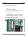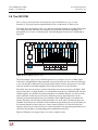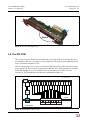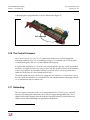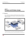
1
Particle Physics & Astrophysics
The New ROD Complex (NRC)
For the ATLAS CSC Electronics
Conceptual Design Report
Document Version:
Document Issue:
Document Edition:
Document Status:
Document ID:
Document Date:
1.1
1
English
First release to reviewers
XXX-TD-xxxxx
September 23, 2012
Stanford Linear Accelerator Center (SLAC )
2575 Sandhill Road
Menlo Park California, 94025 USA
The New ROD Complex (NRC)
September 23, 2012
Conceptual Design Report
Version/Issue: 1.1/1
This document has been prepared using the Software Documentation Layout Templates that have been
prepared by the IPT Group (Information, Process and Technology), IT Division, CERN (The European
Laboratory for Particle Physics). For more information, go to http://framemaker.cern.ch/.
page 2
First release to reviewers
The New ROD Complex (NRC)
Abstract
Conceptual Design Report
Version/Issue: 1.1/1
Abstract
This document describes a joint SLAC National Accelerator Laboratory and UCI (University of
California at Irivine) design proposal, which addresses the need for a replacement of the
current set of ATLAS CSC ROD s (Read-Out-Drivers). The current set is not simply a collection of
VME boards, but is instead composed of a complex aggregate of hardware (PCB boards, VME
crates, power supplies), firmware1 and software. It is that aggregate, not just its 9U VME boards
which is to be replaced. We reference that aggregate as the ROD Complex, its existing
implementation as the Current ROD Complex and its replacement as the New ROD Complex or
NRC . The replacement is driven solely by the need to address performance limitations of the
current complex. Those limitations are described in [16] and it is those limitations that must be
addressed over the LHC‘s first long shutdown. There are neither requirements to add to or
subtract from the functionality of the current complex. Therefore, there is a strong desire to
satisfy those performance limitations within the constraints imposed by the complex’s current
functionality as well as its external interfaces. In short, the proposal must satisfy performance
requirements, do so within its external interfaces and without compromise of current
functionality, and establish robust and reliable operation before data taking restarts after the
long shutdown.
Intended audience
The major impetus for this document is the upcoming conceptual design review and
subsequently, its principal audience is that review’s committee. However, the document also
serves as the initial blueprint for its corresponding design and may therefore, be profitably
read by the audience responsible for its implementation.
Conventions used in this document
Certain special typographical conventions are used in this document. They are documented
here for the convenience of the reader:
—
Acronyms are shown in small caps (e.g., SLAC or CSC ).
—
C++ coding statements are shown in Courier bold (e.g., RIGHT_FIRST or
LAYER_MASK)
1. Where here the term firmware is meant to express the coding languages used in FPGA s.
First release to reviewers
page 3
The New ROD Complex (NRC)
References
Conceptual Design Report
Version/Issue: 1.1/1
References
1
G. Aad et al. [ATLAS Collaboration], The ATLAS Experiment at the CERN Large Hadron
Collider, J. Inst. 3 S08003 (2008), pp. 178-186. Describes the ATLAS Experiment,
Muon spectrometer, TDAQ , Cathode Strip Chambers and front-end electronics. A
copy is available here:
http://www.iop.org/EJ/article/1748-0221/3/08/S08003/jinst8_08_s08003.pdf
2
P. O'Connor et al., READOUT ELECTRONICS FOR A HIGH-RATE CSC
DETECTOR, Fifth Workshop on Electronics for LHC Experiments (Snowmass 1999).
Describes the front-end electronics, but some details have changed. ATLAS
detector paper has the up-to-date information. A copy is available here:
https://twiki.cern.ch/twiki/pub/Atlas/CscDocuments/leb99_oconnor.pdf
3
Gough Eschrich [for the ATLAS Muon Collaboration], Readout Electronics of the ATLAS
Muon Cathode Strip Chambers, in Proceedings of the Topical Workshop on Electronics
for Particle Physics (TWEPP08), Naxos, Greece, 15-19 September 2008, CERN Yellow
Report CERN-2008-008 (also available as CERN-ATL-COM-MUON-2008-018). Most
up-to-date description of CSC readout, emphasis on the off-detector electronics.
A copy is available here:
https://twiki.cern.ch/twiki/pub/Atlas/CscDocuments/TWEPP08.pdf
4
D. Hawkins, ATLAS Particle Detector CSC ROD Software Design and Implementation,
CERN-ATL-COM-MUON-2006-002. DPU software description; extract from
Donovan's thesis. A copy is available here:
http://positron.ps.uci.edu/~ivo/ATLAS/DPU_Documentation.pdf
5
ATCA short specification:
http://www.picmg.org/pdf/picmg_3_0_shortform.pdf
6
ATCA PICMG
7
ASIS 5-slot shelf specification (no longer in production?):
http://www.asis-pro.com/
8
SNAP -12 MSA :
3.0 specification:
http://www.picmg.org/v2internal/specifications.htm
http://www.physik.unizh.ch/~avollhar/snap12msa_051502.pdf
9
Data sheet for Micrel Ulta-Precision 1:8 CML FANOUT BUFFER WITH INTERNAL
I/O TERMINATION. Precision Edge SY58031U
10
MPO / MTP cable. A Very Short Reach (VSR) OC-192 four fiber Interface based on
Parallel Optics. Implementation Agreement OIF-VSR4-03.0
11
Yazaki LC connector product specification. DOC No. OCD-EE-401-1 Version 1.2, July07
12
Pulser Calibration Board:
D. Tompkins, “CSC Pulser rev. H”,
https://twiki.cern.ch/twiki/pub/Atlas/CscPulser/CSC_Pulser_H.pdf
13
page 4
A. Anjos, H. P. Beck, B. Gorini, W. Vandelli, “The raw event format in the ATLAS
Trigger & DAQ”, https://edms.cern.ch/file/445840/4.0e/eformat.pdf
First release to reviewers
The New ROD Complex (NRC)
References
Conceptual Design Report
Version/Issue: 1.1/1
14
CSC
Event Format:
http://positron.ps.uci.edu/~schernau/ROD/2rt/CSCDataFormat.html
15
Private communication David Francis (September 4th, 2012)
16
The New ROD Complex (NRC) Requirements. V0.4 Raul Murillo-Garcia
https://indico.cern.ch/getFile.py/access?contribId=0&resId=0&materialId=slides&confI
d=208888
17
PICMG 3.8:
http://www.picmg.org/v2internal/resourcepage2.cfm?id=2
18
IPMI specification:
http://www.intel.com/design/servers/ipmi/spec.htm
19
Private communication, Markus Joos (September 4th, 2012)
20
SFP Committee. INF-8074i Specification for (Small Formfactor Pluggable) Transceiver.
Rev 1.0 May 12, 2001
21
Kugel, A. et al., ATLAS ROBIN User Manual, CERN,ATL-DQ-ON-0018, Apr
2006, https://edms.cern.ch/file/719553/1/robinUserManual.pdf,
Cranfield, R. et al., The ATLAS ROBIN, Journal of Instrumentation, JINST 3
T01002, Jan 2008, http://dx.doi.org/10.1088/1748-0221/3/01/T01002,
Crone, G. et al., The ATLAS ReadOut System - performance with first data and
perspective for the future, Acc. for publication in proceedings of The 1st international
conference on Technology and Instrumentation in Particle Physics, Tsukuba,
Japan,Mar 12-172009,
http://cdsweb.cern.ch/record/1193091/files/ATL-DAQ-PROC-2009-025.pdf
22
http://positron.ps.uci.edu/~schernau/sparse.ps
23
http://positron.ps.uci.edu/~pier/csc/CTM/CTM_ReferenceManual_01.pdf
24
http://positron.ps.uci.edu/~pier/csc/ROD_ASMII_Interface0.pdf
25
http://hsi.web.cern.ch/hsi/s-link/devices/hola/
26
O. Boyle1, R. McLaren and E. v. der Bij, “The S-LINK Interface Specification”,
https://edms.cern.ch/file/110828/4/s-link.pdf
http://hsi.web.cern.ch/HSI/s-link/
27
http://subversion.apache.org/
28
https://svnweb.cern.ch/cern/wsvn/muondaq?
29
ATLAS CSC
30
SLAC Detector R&D DAQ wiki,
https://confluence.slac.stanford.edu/display/CCI/DAT+Home
31
RTEMS
32
http://www.xilinx.com/
33
http://en.wikipedia.org/wiki/VHDL
wiki, https://twiki.cern.ch/twiki/bin/viewauth/Atlas/CathodeStripChambers
Real Time Operating System, http://www.rtems.com/
First release to reviewers
page 5
The New ROD Complex (NRC)
References
34
http://www.gnu.org/
35
https://twiki.cern.ch/twiki/bin/viewauth/Atlas/CSCTestProcedures
36
https://twiki.cern.ch/twiki/bin/viewauth/Atlas/ReleaseNotes
37
http://positron.ps.uci.edu/~pier/
38
Fulcrum Focalpoint FM2224, 24-port 10G Ethernet L2 Switch Chip. Advanced
Information Data Sheet. February 2006 (revision 0.7)
39
P. Gällnö, “ATLAS ROD Busy Module. Technical description and users manual”,
https://edms.cern.ch/file/319209/1/rod_busy_manual_2.pdf
40
P. Gällnö, “ATLAS Local Trigger Processor - LTP. Technical description and users
manual”, https://edms.cern.ch/file/551992/2/LTP_manual_041.pdf
41
Pigeon-Point documentation
http://www.pigeonpoint.com/pdf/ShelfManagerUG.pdf
42
“ATLAS Level-1 Trigger Technical Design Report (Chapter 16) “,
http://atlas.web.cern.ch/Atlas/GROUPS/DAQTRIG/TDR/V1REV1/L1TDR_TTC. pdf
43
J. Christiansen, A. Marchioro, P. Moreira and T. Toifl, “TTCrx Reference Manual”,
https://edms.cern.ch/file/1148404/1/TTCrx_manual3.11.pdf
44
The ATLAS Level-1 Central Trigger Processor Core Module (CTP_CORE),
cdsweb.cern.ch/record/801863/files/n22-4-slides.pdf
45
G. Lehmann, “ATLAS TDAQ Controls: Operations at Different Activity Stages”,
https://edms.cern.ch/file/675671/1/ATLAS_OperationsAndTransitions.pdf
46
ATLAS Detector Control System (DCS),
https://twiki.cern.ch/twiki/bin/viewauth/Atlas/AtlasDcs
47
I. Soloviev, “ATLAS TDAQ Config Packages”,
http://atlas-tdaq-sw.web.cern.ch/atlas-tdaq-sw/doxygen/tdaq/production/html/ConfigPac
kages.html
48
S. Kolos, “ATLAS TDAQ How to use the ERS package”, http://atlas-tdaqsw.web.cern.ch/atlas-tdaq-sw/doxygen/tdaq-common/production/html/main.html
http://atlasdaq.cern.ch/jnlp/logmanager/logmanager.jnlp
S. Kolos, “Information Service user’s guide”,
http://atlas-tdaq-monitoring.web.cern.ch/atlas-tdaq-monitoring/IS/doc/userguide/is-user
sguide.pdf
“Online Histogramming”, http://atlas-onlsw.web.cern.ch/Atlas-onlsw/oh/oh.htm
“OHP Monitoring”, https://twiki.cern.ch/twiki/bin/viewauth/Atlas/OhpMonitoring
“Incremental Design Reuse with Partitions. Xilinx application note: XAPP918 (v1.0)
June 7, 2007.
Zynq-7000 All programmable SoC Overview DS190 (v1.2) August 21, 2012.
Virtex-5 Family overview. DS100 (v5.0) February 6, 2009
Embedded Processor Block in Virtex-5 FPGAs. Reference Guide. UG200 (v1.8).
February 24, 2010
49
50
51
52
53
54
55
56
page 6
Conceptual Design Report
Version/Issue: 1.1/1
First release to reviewers
The New ROD Complex (NRC)
Document Control Sheet
Conceptual Design Report
Version/Issue: 1.1/1
Document Control Sheet
Table 1 Document Control Sheet
Document
Tools
Authorship
Title:
The New ROD Complex (NRC) Conceptual Design Report
Version:
1.1
Issue:
1
Edition:
English
ID:
XXX-TD-xxxxx
Status:
First release to reviewers
Created:
September 1, 2012
Date:
September 23, 2012
Access:
V:\REG\Detector Rand D\NRC\CDR\V1.1\frontmatter.fm
Keywords:
CSC ROD
DTP System:
Adobe FrameMaker
Version:
6.0
Layout
Template:
Software Documentation
Layout Templates
Version:
V2.0 - 5 July 1999
Content
Template:
--
Version:
--
Coordinator:
Michael Huffer, SLAC
Written by:
Richard Claus (SLAC), Raul Murillo Garcia (UCI), Ryan T. Herbst
(SLAC), Andrew J. Lankford (UCI), Andrew Nelson (UCI), Su Dong
(SLAC), Nicoletta Garelli (SLAC), Rainer Bartoldus (SLAC), James
Russell (SLAC)
First release to reviewers
page 7
The New ROD Complex (NRC)
Document Status Sheet
Conceptual Design Report
Version/Issue: 1.1/1
Document Status Sheet
Table 2 Document Status Sheet
page 8
Title:
The New ROD Complex (NRC) Conceptual Design Report
ID:
XXX-TD-xxxxx
Version
Issue
Date
Reason for change
0.1
1
9/1/2012
First (very rough) look for the SLAC and UCI folk
0.5
1
9/18/2012
Finished COB and RTM sections, general cleanup of chapter 3.
0.6
1
9/20/2012
Finished FTM, Base board, Control Processor, Mezzanine
board sections. Did some other general cleanup. Updated
chapter 3 reflecting input from yesterday’s review.
0.7
1
9/21/2012
Initial draft of RCE section. Did some other general cleanup.
More cleanup of chapter 3.
0.8
1
9/22/2012
Initial draft of CE software section. Added detail to photographs. Added to references and did other general cleanup.
1.0
1
9/23/2012
First release for reviewers
1.1
1
9/24/2012
First typos found by Rainer & Raul
First release to reviewers
The New ROD Complex (NRC)
List of Tables
Conceptual Design Report
Version/Issue: 1.1/1
List of Tables
Table 1
p. 7
Document Control Sheet
Table 2
p. 8
Document Status Sheet
First release to reviewers
page 9
The New ROD Complex (NRC)
List of Tables
page 10
Conceptual Design Report
Version/Issue: 1.1/1
First release to reviewers
The New ROD Complex (NRC)
Table of Contents
Conceptual Design Report
Version/Issue: 1.1/1
Table of Contents
.
.
.
.
.
.
.
.
.
.
.
.
.
.
.
.
.
.
.
.
.
.
.
.
.
.
.
.3
Intended audience .
.
.
.
.
.
.
.
.
.
.
.
.
.
.
.
.
.
.
.
.
.
.
.
.
.
.
.3
Conventions used in this document .
.
.
.
.
.
.
.
.
.
.
.
.
.
.
.
.
.
.
.
.
.3
Abstract
.
.
.
.
.
.
.
.
.
.
.
.
.
.
.
.
.
.
.
.
.
.
.
.
.
.
.
.4
Document Control Sheet .
.
.
.
.
.
.
.
.
.
.
.
.
.
.
.
.
.
.
.
.
.
.
.
.
.7
Document Status Sheet .
.
.
.
.
.
.
.
.
.
.
.
.
.
.
.
.
.
.
.
.
.
.
.
.
.8
List of Tables .
.
.
.
.
.
.
.
.
.
.
.
.
.
.
.
.
.
.
.
.
.
.
.
.
.
.
.
.
.9
List of Figures
.
.
.
.
.
.
.
.
.
.
.
.
.
.
.
.
.
.
.
.
.
.
.
.
.
.
.
. 15
List of Listings .
.
.
.
.
.
.
.
.
.
.
.
.
.
.
.
.
.
.
.
.
.
.
.
.
.
.
. 17
Chapter 1
Overview .
.
.
.
.
.
.
.
.
.
.
.
.
.
.
.
.
.
.
.
.
.
.
.
.
.
.
. 19
1.1 Introduction . . . . . . . . . . .
1.2 The CSC and its On-Detector Electronics
1.3 Input rates . . . . . . . . . . .
1.4 The ROS Complex . . . . . . . .
1.5 Feature extraction & output rates . . .
1.6 Power and footprint . . . . . . . .
1.7 Environmental Monitoring & Control .
1.8 Trigger & Timing Control (TTC) . . .
1.9 Busy handling . . . . . . . . . .
1.10 TDAQ Control and Monitoring . . .
.
.
.
.
.
.
.
.
.
.
.
.
.
.
. 19
.
.
.
.
.
.
.
.
.
.
.
.
.
.
. 20
.
.
.
.
.
.
.
.
.
.
.
.
.
.
. 21
.
.
.
.
.
.
.
.
.
.
.
.
.
.
. 21
.
.
.
.
.
.
.
.
.
.
.
.
.
.
. 22
.
.
.
.
.
.
.
.
.
.
.
.
.
.
. 22
.
.
.
.
.
.
.
.
.
.
.
.
.
.
. 22
References
.
.
.
.
.
.
.
First release to reviewers
.
.
.
.
.
.
.
.
.
.
.
.
.
.
. 23
.
.
.
.
.
.
.
.
.
.
.
.
.
.
. 23
.
.
.
.
.
.
.
.
.
.
.
.
.
.
. 23
page 11
The New ROD Complex (NRC)
Table of Contents
Chapter 2
Physical Design .
Conceptual Design Report
Version/Issue: 1.1/1
.
.
.
.
.
.
.
.
.
.
.
2.1 ATCA as the implementation platform
2.1.1 The Shelf . . . . . . . . .
2.1.2 Shelf Power . . . . . . . .
2.1.3 The Front-Board . . . . . .
2.1.4 The RTM . . . . . . . . .
2.1.5 IPMI and the Shelf Manager . .
2.2 Overview . . . . . . . . . . .
2.3 Shelf choice . . . . . . . . . .
2.4 Shelf Power . . . . . . . . . .
2.5 Shelf Manager & IPMI . . . . . .
2.6 The COB . . . . . . . . . . .
2.6.1 The DTM Bay . . . . . . .
2.6.2 The DPM bay . . . . . . .
2.6.3 Fabric Interconnect . . . . .
2.6.4 Base Interconnect . . . . .
2.6.5 The ATLAS FTM . . . . . .
2.6.6 The ATLAS Base Board . . .
2.7 The RCE . . . . . . . . . . .
2.7.1 The Protocol-Plug-In . . . .
2.7.2 The Cluster Element . . . .
2.7.3 CE Software Services . . . .
2.7.4 The Mezzanine board . . . .
2.8 The CSC RTM . . . . . . . . .
2.9 The SFP RTM . . . . . . . . .
2.10 The Control Processor . . . . . .
2.11 Networking . . . . . . . . .
Chapter 3
Firmware and Software design
.
.
.
3.1 Introduction . . . . . . .
3.2 The Event Plane . . . . .
3.2.1 Input Plug-in . . . .
3.2.2 FEX Plug-in . . . . .
3.2.3 S-Link Plug-in . . . .
3.2.4 Usage . . . . . . .
3.3 Trigger Plane . . . . . .
3.3.1 SCA Controller . . .
3.3.2 TTC Receiver Plug-in .
3.3.3 TTC Transmitter Plug-in
3.4 Busy Plane . . . . . . .
page 12
.
.
.
.
.
.
.
.
.
.
.
.
.
.
.
. 25
.
.
.
.
.
.
.
.
.
.
.
.
.
.
.
. 25
.
.
.
.
.
.
.
.
.
.
.
.
.
.
.
. 25
.
.
.
.
.
.
.
.
.
.
.
.
.
.
.
. 28
.
.
.
.
.
.
.
.
.
.
.
.
.
.
.
. 28
.
.
.
.
.
.
.
.
.
.
.
.
.
.
.
. 29
.
.
.
.
.
.
.
.
.
.
.
.
.
.
.
. 30
.
.
.
.
.
.
.
.
.
.
.
.
.
.
.
. 31
.
.
.
.
.
.
.
.
.
.
.
.
.
.
.
. 33
.
.
.
.
.
.
.
.
.
.
.
.
.
.
.
. 34
.
.
.
.
.
.
.
.
.
.
.
.
.
.
.
. 34
.
.
.
.
.
.
.
.
.
.
.
.
.
.
.
. 35
.
.
.
.
.
.
.
.
.
.
.
.
.
.
.
. 36
.
.
.
.
.
.
.
.
.
.
.
.
.
.
.
. 37
.
.
.
.
.
.
.
.
.
.
.
.
.
.
.
. 37
.
.
.
.
.
.
.
.
.
.
.
.
.
.
.
. 38
.
.
.
.
.
.
.
.
.
.
.
.
.
.
.
. 39
.
.
.
.
.
.
.
.
.
.
.
.
.
.
.
. 39
.
.
.
.
.
.
.
.
.
.
.
.
.
.
.
. 40
.
.
.
.
.
.
.
.
.
.
.
.
.
.
.
. 42
.
.
.
.
.
.
.
.
.
.
.
.
.
.
.
. 43
.
.
.
.
.
.
.
.
.
.
.
.
.
.
.
. 44
.
.
.
.
.
.
.
.
.
.
.
.
.
.
.
. 45
.
.
.
.
.
.
.
.
.
.
.
.
.
.
.
. 47
.
.
.
.
.
.
.
.
.
.
.
.
.
.
.
. 48
.
.
.
.
.
.
.
.
.
.
.
.
.
.
.
. 49
.
.
.
.
.
.
.
.
.
.
.
.
.
.
.
. 49
.
.
.
.
.
.
.
.
.
.
.
.
.
.
.
.
.
.
. 51
.
.
.
.
.
.
.
.
.
.
.
.
.
.
.
.
.
.
. 51
.
.
.
.
.
.
.
.
.
.
.
.
.
.
.
.
.
.
. 52
.
.
.
.
.
.
.
.
.
.
.
.
.
.
.
.
.
.
. 54
.
.
.
.
.
.
.
.
.
.
.
.
.
.
.
.
.
.
. 55
.
.
.
.
.
.
.
.
.
.
.
.
.
.
.
.
.
.
. 55
.
.
.
.
.
.
.
.
.
.
.
.
.
.
.
.
.
.
. 55
.
.
.
.
.
.
.
.
.
.
.
.
.
.
.
.
.
.
. 56
.
.
.
.
.
.
.
.
.
.
.
.
.
.
.
.
.
.
. 56
.
.
.
.
.
.
.
.
.
.
.
.
.
.
.
.
.
.
. 58
.
.
.
.
.
.
.
.
.
.
.
.
.
.
.
.
.
.
. 58
.
.
.
.
.
.
.
.
.
.
.
.
.
.
.
.
.
.
. 58
First release to reviewers
The New ROD Complex (NRC)
Table of Contents
Conceptual Design Report
Version/Issue: 1.1/1
3.4.1 Busy Source Plug-in . . . .
3.4.2 Busy Destination Plug-in . . .
3.5 TDAQ Plane . . . . . . . . .
3.6 Firmware and Software Maintenance
3.7 Software tools . . . . . . . . .
3.8 Test and Release plan . . . . . .
3.9 System monitoring . . . . . . .
3.10 Calibration . . . . . . . . . .
.
.
.
.
.
.
.
.
.
.
.
.
.
.
.
. 60
.
.
.
.
.
.
.
.
.
.
.
.
.
.
.
. 60
.
.
.
.
.
.
.
.
.
.
.
.
.
.
.
. 60
.
.
.
.
.
.
.
.
.
.
.
.
.
.
.
. 62
.
.
.
.
.
.
.
.
.
.
.
.
.
.
.
. 62
.
.
.
.
.
.
.
.
.
.
.
.
.
.
.
. 62
.
.
.
.
.
.
.
.
.
.
.
.
.
.
.
. 63
.
.
.
.
.
.
.
.
.
.
.
.
.
.
.
. 63
First release to reviewers
page 13
The New ROD Complex (NRC)
Table of Contents
page 14
Conceptual Design Report
Version/Issue: 1.1/1
First release to reviewers
The New ROD Complex (NRC)
List of Figures
Conceptual Design Report
Version/Issue: 1.1/1
List of Figures
Figure 1
p. 19
Interfaces for the The ROD Complex
Figure 2
p. 26
Front view of an ASIS 5-slot ATCA shelf
Figure 3
p. 27
Rear view of an ASIS 5-slot ATCA shelf
Figure 4
p. 28
Exposed view of an ASIS 5-slot ATCA shelf’s backplane
Figure 5
p. 29
Representative ATCA Front-Board
Figure 6
p. 30
Representative ATCA RTM
Figure 7
p. 32
Block Diagram of the New ROD Complex
Figure 8
p. 35
Preproduction COB
Figure 9
p. 36
Block Diagram of the COB
Figure 10
p. 39
Prototype FTM
Figure 11
p. 41
Block Diagram of the RCE
Figure 12
p. 43
Block Diagram of the CE
Figure 13
p. 46
Preproduction COB -Mezzanine-Board (CMB )
Figure 14
p. 47
Block diagram of the CSC RTM
Figure 15
p. 48
An RTM containing SNAP -12s
Figure 16
p. 48
Block diagram of the SFP RTM
Figure 17
p. 49
An RTM containing SFP s
Figure 18
p. 51
NRC
Figure 19
p. 53
Event Flow
Figure 20
p. 56
Trigger Flow
Figure 21
p. 59
Busy Flow
Figure 22
p. 60
Run-Control Flow
dataflow through it interfaces
First release to reviewers
page 15
The New ROD Complex (NRC)
List of Figures
page 16
Conceptual Design Report
Version/Issue: 1.1/1
First release to reviewers
The New ROD Complex (NRC)
List of Listings
Conceptual Design Report
Version/Issue: 1.1/1
List of Listings
First release to reviewers
page 17
The New ROD Complex (NRC)
List of Listings
page 18
Conceptual Design Report
Version/Issue: 1.1/1
First release to reviewers
The New ROD Complex (NRC)
Chapter 1 Overview
Conceptual Design Report
Version/Issue: 1.1/1
Chapter 1
Overview
1.1 Introduction
The ROD Complex’s principal responsibility is for the acquisition and extraction of data from
the ATLAS muon system’s Cathode Strip Chambers (CSC ) along with their resulting transfer to
the ATLAS TDAQ system. Acquisition is driven externally by the ATLAS central trigger system
at its L1A rate. To support this activity the complex is also responsible for the setup, control
and monitoring of the on-detector electronics associated with those chambers. Treating for the
moment that complex as a black box, its potential replacement must, at a minimum, satisfy its
interfaces. Those interfaces are illustrated in Figure 1:
CSC On-Detector-Electronics
MPO F/O x 32
MPO F/O x 16
True-Light F/O
1G-Ethernet (copper)
TDAQ Control & Monitoring
Trigger Timing & Control (TTC)
ROD
COMPLEX
Busy
Environmental Control & Monitoring (DCS)
Power & Footprint
LEMO (copper)
L/C F/O x 8
L/C F/O x 8
ROSa
ROSb
NRC/FIGURES/INTERFACES
Figure 1 Interfaces for the The ROD Complex
The remainder of this chapter serves as an introduction to those interfaces as well as to the
performance required of its replacement. Note that much of the identical information is
contained, albeit with a different emphasis, in [16].
First release to reviewers
page 19
The New ROD Complex (NRC)
Chapter 1 Overview
Conceptual Design Report
Version/Issue: 1.1/1
Chapter 2 introduces the physical design of its replacement. Two somewhat unique features of
the replacement proposal are:
i.
The substitution of ATCA for VME as an implementation platform.
ii.
The usage of building blocks from SLAC ’s DAQ tool-box (the RCE and COB ).
Consequently, to fully communicate the proposal requires some rudimentary understanding
of ATCA as well as the above mentioned building blocks. The second chapter is intended to
provide background for both.
The usage of both ATCA and these blocks is the principal feature of this proposal. Within the
constraints of an 18 month schedule this feature makes it practical to propose the design,
fabrication, testing & integration of what logistically amounts to the production of an entirely
new set of ROD s.
Further, this feature turns its replacement from a hardware to software-centric design. The
amount of hardware to be designed and fabricated as compared to what must be purchased
and integrated is quite modest. Therefore, the bulk of engineering entailed by this proposal
resides in its firmware and software. Chapter 3 introduces and describes that firmware and
software design.
1.2 The CSC and its On-Detector Electronics
The CSC consists of thirty-two (32) chambers. Each chamber contains four (4) precision layers of
192 channels each and four (4) transverse layers of 48 channels each. The on-detector
electronics are partitioned into units of ASM-II Boards [2]. One ASM-II board is designed to
process 192 channels of data. Consequently, each chamber contains five ASM-II boards; four
managing the chamber’s precision layers and one its transverse layer. Chamber data are
sampled every 50 ns. One sample from one channel produces 12-bits of data. One sample from
all 192 channels of a chamber is called a Time-Slice. In nominal data taking mode each L1A
from the trigger generates four time-slices. Therefore, when configured for nominal operation,
the amount of data emitted by one ASM-II is approximately 9.216 Kbits (1.15 Kbytes), and for
an entire chamber, five times that value or approximately 46.080 Kbits (5.76 Kbytes), and for the
entire CSC , thirty-two times that value or approximately 1.475 Mbits (184 Kbytes). Note, the
chambers emit data which is not sparse and therefore the amount of data transmitted by an
ASM-II per event is independent of beam conditions as well as L1A rate.
Each ASM-II has three (3) fiber-optic links. Two of its three links operate as a pair and are used
for transmission (downlink) of chamber data, while the third receives (uplinks) external
control and timing. Independent of their direction all links are synchronized to the ATLAS
system clock (40 MHZ ) and operate at 640 Megabits/second. However, as transmitters work in
pairs the downlink capacity of one ASM-II is twice that value, or 1.28 Gigabits/second1.
The downlink for one chamber requires ten (10) fiber-optic links. Those ten links are bundled
into one, twelve (12) strand fiber-optic MPO cable [10], leaving two of the twelve strands
1. Roughly 160 Mbytes/second.
page 20
First release to reviewers
The New ROD Complex (NRC)
Chapter 1 Overview
Conceptual Design Report
Version/Issue: 1.1/1
unused. The uplink for a single chamber requires six (6) fiber-optic links. Five of those links
receive the ASM-II’s timing and control, while the sixth is used to drive the chamber’s pulser
calibration board [11]. The uplinks for two chambers are bundled together into a single MPO
cable. It is these existing MPO uplink and downlink cables which define the on-detector
electronics interface to the complex. As the CSC contains thirty-two chambers, there are in
total forty-eight (48) cables, thirty-two (32) downlink and sixteen (16) uplink.
1.3 Input rates
To satisfy its primary performance requirement the complex must process chamber data up to
the maximum L1A rate, which is defined as 100 KHZ Poisson averaged. This implies the
maximum data rate produced by a single ASM-II board is approximately 115 MBytes/second
and for a single chamber five times that value or approximately 576 Mbytes/second. With
thirty-two (32) chambers the entire complex must absorb thirty-two times that value, or a
value somewhat greater than 18 GBytes/second.
1.4 The ROS Complex
Feature extracted event data are the product of the complex. Those data are sent in parallel
from the ROD complex to the TDAQ system. That unit of parallelism is the ROL (Read-Out Link).
The ROL is a single, full-duplex, fiber-optic link operating at 1.28 Gigabits/second [21]. Data are
sent on one duplex and flow-control received on its other. Physically, the ROL uses single
mode fiber and is terminated at both ends with L/C connectors [11].
Data transmitted by the ROL must conform to the envelope dictated by the protocol specified
in [13]. That protocol specifies that one event produces one frame. For the CSC , the event data
produced from two (2) chambers is carried on one (1) ROL . The structure of one frame is
described in [14].
Data for the entire complex is sent on sixteen (16) ROL s. The component of the TDAQ system
that receives and manages output from ROLS is the ROS (Read-Out-System). The CSC requires
two (2), one allocated to each of its two endcaps. That is, each ROS services the CSC data from
eight (8) ROL s.
In short, it is those existing sixteen ROL s which define the TDAQ event or ROS interface to the
complex.
First release to reviewers
page 21
The New ROD Complex (NRC)
Chapter 1 Overview
Conceptual Design Report
Version/Issue: 1.1/1
1.5 Feature extraction & output rates
The data volume numbers described in Section 1.3 represent the input rate to the complex.
However, it’s important to note, unlike most ATLAS subsystems the amount of data into the
CSC ’s complex is not equal to the amount of data out of its complex. For any given event, the
CSC ‘s chambers emit their entire response, presenting a somewhat significant data volume.
However, as chamber occupancy for any given event is quite modest, the amount of
corresponding signal emitted by the CSC is also quite modest. It remains the complex’s
responsibility as well as one of its principal requirements to extract that signal and forward
only those data representing hit channels in the CSC chambers. The process of identifying that
signal will be referred to as Feature Extraction (FEX ). Although described in detail in [4], feature
extraction involves a threshold cut, out-of-time rejection as well as cluster finding. Its
implementation for the NRC is described in Section 3.2.
Output size is then, of course, a function of chamber occupancy, which in turn varies with
luminosity, pile-up and background. These effects can be parameterized by the single number
mu, which is the average number of interactions per bunch crossing. For example, at a mu of
thirty (30), representative of today’s typical operating conditions, the size of an output event is
on the order of 150 bytes per chamber.
To insure a healthy safety margin the requirements on the NRC are set at a mu expected after
Phase-1 turn-on. That mu is eighty (80), resulting in an expected output event size of
approximately 570 bytes per chamber, per event [16].
Recall (see above, Section 1.4) that data from two chambers are carried on one ROL , giving at a
mu of 80, 1140 bytes per ROL , per event.
At an L1A rate of 100 KHZ , this leads to an output data rate of about 57 Mbytes/second per
chamber or for a single ROL double that value or 114 Mbytes/second per ROL . Assuming a
normal distribution between the CSC ’s two endcaps this corresponds to somewhat less than
one (1) Gbyte/second per ROS .
1.6 Power and footprint
See [16].
1.7 Environmental Monitoring & Control
The Detector Control System (DCS ) [46] has the responsibility to monitor and control detector
infrastructure such as power supplies and ventilation.
page 22
First release to reviewers
The New ROD Complex (NRC)
Chapter 1 Overview
Conceptual Design Report
Version/Issue: 1.1/1
1.8 Trigger & Timing Control (TTC)
The Trigger and Timing Control system is described in [42] and [43]. It consists of a Central
Trigger Processor (CTP ) [44] and a distributed set of Local Trigger Processors (LTP s) [40].
1.9 Busy handling
The ‘BUSY’ signal generated by the ROD Complex is consumed by the Busy Module [39]. This
module aggregates the BUSY signals on its inputs into a single output signal that is ultimately,
possibly via other Busy Modules, forwarded to the Central Trigger Processor (CTP ) [44]. When
BUSY is assert to the CTP , triggers are inhibited from being propagated to the subsystems via
their individual Local Trigger Processors (LTP ) [40].
1.10 TDAQ Control and Monitoring
The TDAQ Control system is based on a Finite State Machine (FSM ) model, as described in [45].
Besides controlling the operation of the ATLAS experiment for taking data, the system
monitors various aspects of the operation.
The TDAQ software suite is comprised of a variety of packages such as the Configuration
Package [47], the Error Reporting System [48], the Log Manager [49][50], Histogramming
[51][52], etc. Through the use of these packages, the CSC subsystem can be put through its
paces, in both stand-alone situations as well as combined ATLAS running.
First release to reviewers
page 23
The New ROD Complex (NRC)
Chapter 1 Overview
page 24
Conceptual Design Report
Version/Issue: 1.1/1
First release to reviewers
The New ROD Complex (NRC)
Chapter 2 Physical Design
Conceptual Design Report
Version/Issue: 1.1/1
Chapter 2
Physical Design
2.1 ATCA as the implementation platform
The New ROD Complex (NRC ) is designed as a plug compatible replacement for the current
complex. The interfaces necessary to satisfy that plug compatibility were described in Chapter
1. At one level of abstraction the physical implementation of the NRC could be simply
represented as an arbitrary aggregate of PCB boards. But, of course, because these boards
operate to a single purpose, they will also necessarily require connections between them.
Typically, for reasons of understanding, modularity and maintenance, those connections
follow predefined, accepted mechanical and electrical standards. In this document any such
usage which employs a specific standard will be referenced as a Platform. For example, VME
would constitute one such platform. For the NRC that platform is based on an existing
standard developed by the PCI Industrial Computer Manufactures Group (PICMG) commonly
referred to as the Advanced Tele-Communication Architecture, or ATCA , whose current revision is
referred to within that consortium as PICMG 3.0. As a platform ATCA is now quite mature,
having been in existence for more than ten years, with a broad design base and a wealth of
equipment deployed in the field as well as a burgeoning eco-structure within the
telecommunication and defence industries.
usage by the NRC will be entirely compliant with the PICMG 3.0 specification. That
specification is described in [6] with an introduction available from [5]. However, the
remainder of this section is intended to provide sufficient background to gain a thorough
understanding of the physical design description.
ATCA
2.1.1 The Shelf
The ATCA shelf is known historically as the chassis and is by analogy, equivalent to a VME crate.
Shelves house the Front-Boards and RTM s described below (see Sections 2.1.3 and 2.1.4). They
contain, from front to rear, pairs of slots with each pair housing a Front-Board in the front and
the Front-Boards’s corresponding RTM in the rear. The shelf allows for hot-swap of any board
in any slot. Depending on form factor the number of its slot pairs varies from two (2) to sixteen
First release to reviewers
page 25
The New ROD Complex (NRC)
Chapter 2 Physical Design
Conceptual Design Report
Version/Issue: 1.1/1
(16). The orientation of those slots also varies, as shelves are offered with either horizontal or
vertical orientation. In turn, that orientation affects the flow of air; from either left to right
(horizontal), or top to bottom (vertical).
Broadly, the shelf is composed of a subrack, backplane, filters and cooling devices (fans). The
subrack provides the infrastructure to contain the Front-Boards and RTM s described below.
This includes guide rails, ESD discharge, alignment, keying, and backplane interface.
Backplanes are passive circuit boards which carry the connections between slots. Although
somewhat more complicated in detail, for this document, those connections can be
partitioned into three logical groups: power, control and differential data pairs. The topology
for both power and control connections is invariant of backplane. However, in order to
accommodate different applications the connection topology of data pairs can vary. Two
commonly used topologies are the dual star and full mesh.The backplane (and ATCA ) is
protocol agnostic with respect to the usage of these differential pairs with the choice delegated
to the shelf’s specific Front-Boards.
Figure 2 provides a front view of a representative ATCA shelf as used for development by
SLAC ’s Detector R & D program:
Shelf Manager
Power supply
Figure 2 Front view of an ASIS 5-slot ATCA shelf
This photograph is of a COTS 1 shelf purchased from ASIS [7]. It has a horizontal orientation
within its corresponding rack with airflow from left to right. It contains a replicated, full mesh
backplane. Two of its five front slots are populated with Front-Boards, while its unused slots
are populated with dummy air baffles. Note the RJ45 connector located on the front-panel of
its Shelf-Manager (ShMC ). This provides the shelf manager access to the Ethernet from which
control and monitoring (through IPMI ) of the shelf would be accomplished. Further, note the
integral power supplies. These supplies are not required by the ATCA standard, but are
provided by ASIS as a convenient feature for bench-top usage. The same shelf viewed from the
rear is illustrated in Figure 3:
1. Commercial-Off-The-Shelf.
page 26
First release to reviewers
The New ROD Complex (NRC)
Chapter 2 Physical Design
Conceptual Design Report
Version/Issue: 1.1/1
External Power
Figure 3 Rear view of an ASIS 5-slot ATCA shelf
As was the case for the front, two of its five rear slots are also populated, however, with RTM s
(see Section 2.1.4) rather than Front-boards. Note, as was the case for the front slots, unused
slots are populated with dummy air baffles. Further, note the power pins provided for
external input of shelf power (+48 VDC). Last, Figure 4 provides an identical view, although
now unpopulated, offering an unobstructed view of its backplane. Note the open area on the
right allowing access to the P3 zones between Front-boards and corresponding RTM .
First release to reviewers
page 27
The New ROD Complex (NRC)
Chapter 2 Physical Design
Conceptual Design Report
Version/Issue: 1.1/1
Zone 3
Figure 4 Exposed view of an ASIS 5-slot ATCA shelf’s backplane
The choice of shelf for the NRC is discussed in Section 2.1.1.
2.1.2 Shelf Power
An ATCA shelf does not have any requirement for provision of its own power. Further, a shelf
also has no explicit requirement for the control and monitoring of that power independent of
source. Instead, its minimum requirement is to simply support external connections for both
primary and redundant supplies. Those supplies must provide +48 VDC . In a large scale
installation this “feature” allows for rack aggregation of power over many shelves.
Power for the NRC shelf is discussed in Section 2.4.
2.1.3 The Front-Board
The Front-Board constitutes the heart of the ATCA eco-system. From a shelf’s perspective that
board is simply a PCB board, 8U wide x 280 mm deep and which plugs into one of its front
slots. That board, although following ATCA mechanical and electrical interface standards,
contains logic which is application specific. And from that logic’s perspective the shelf exists
simply to provide a platform to serve its application specific content.
On its near side the board’s front-panel contains a hot-swap handle as well as four ATCA
defined LED s to help direct an operator in board insertion and removal. The remainder of the
panel is considered application specific. The board’s rear side contains three logical “Zones”.
Zones 1 and 2 connect directly to a shelf’s backplane. Zone 1 provides access to shelf power
(+48 VDC ) as well as the I 2C communication channels which the board uses to communicate
with its shelf manager. Zone 2 provides access to the high-speed, differential pairs connecting
boards together. The area encompassed by Zone 3 is application defined, but reserved for
connections to the board’s RTM . PICMG defines an extension to the standard which allocates
page 28
First release to reviewers
The New ROD Complex (NRC)
Chapter 2 Physical Design
Conceptual Design Report
Version/Issue: 1.1/1
that area. This standard is PICMG 3.8 (“ATCA for physics”, [23]), which follows the convention
of Zone 1 and 2 and partitions its area into two zones, one for power/control and the other for
signals. The connector used for signals allows for allocation of up to 120 differential pairs
between board and RTM .
Any and all boards used by the NRC adhere to PICMG 3.8.
Note, that independent of any allocation scheme for Zone 3 the power for an RTM , if defined,
must go through the Front-Board.
Each board must also contain a local controller called its IPM Controller, or IPMC. The IPMC
manages the board’s activation/deactivation policy as well as monitors its health and safety.
It serves as a proxy to the board’s shelf manager and communicates using the I 2C channels on
Zone 1. The IPMC , as was the case for the board itself, must satisfy ATCA interface standards,
but its implementation is also, necessarily, application specific.
The standard specifies that the sum of the power drawn from a Front-Board and its
corresponding (if any) RTM must not exceed 300 Watts.
The NRC requires one application specific Front-Board. That board is described in Section 2.6.
A photograph of a representative Front-Board, showing connectivity to an RTM (using PICMG
3.8) is illustrated in Figure 5:
RTM
Zone 3 (PICMG 3.8)
hot-swap handles
Zone 2
Zone 1
Figure 5 Representative ATCA Front-Board
2.1.4 The RTM
The RTM (Rear-Transition-Module) is simply a PCB board, 8U wide x 70 mm deep which is used
to extend a Front-Board (see Section 2.1.3). Although not required, that extension is typically
First release to reviewers
page 29
The New ROD Complex (NRC)
Chapter 2 Physical Design
Conceptual Design Report
Version/Issue: 1.1/1
found necessary for two reasons: First, to increase the useful footprint of the Front-Board and
second, to house a board’s external, I/ O interface. The RTM shares the same hot-swap model
as the Front-Board and specifies an identical pitch (1.2”). This allows the RTM to reuse the
same panel, handle switches, and LED s as its Front-board. The RTM connects to its Front-board
through Zone 3. The form of that connection is application specific. However, if power for the
RTM is necessary, it must be provided by the Front-board and must be brought through Zone
3. The ATCA specification is somewhat ambiguous with respect to the maximum power
drawn by an RTM . A shelf is required to provide at a minimum 15 watts of cooling, but is,
however, free to provide more. This is typically the case for all shelf manufacturers with
maximum numbers more in the 40 to 70 watt range.
The RTM s employed by the NRC standardize the usage of Zone 3 by application of PICMG 3.8
[17]. That standardization allows such an RTM to “plug and play” with the NRC ‘s Front-Board
(see Section 2.6). PICMG 3.8 populates Zone 3 with two connectors, one for power and one for
signal. Power provided through the power connector is +12 VDC and that connector also
contains pins for JTAG as well as I2C support. The I2C channel is expected to be used by the
Front-Board for control of the RTM ’s hot-swap switch as well as its front panel LED s.
The signal connector provides up to 120 differential pairs. How those pairs are assigned
between Front-Board and RTM is considered application specific. However, for the NRC ’s
Front-Board, each one of its four DPM bays is assigned 1/4 of those pins or thirty (30) pairs (see
Section 2.6).
The two types of RTM s contained in the NRC are described in Sections 2.8 and 2.9. Figure 6
illustrates a representative RTM showing its PICMG 3.8 interface connected to a Front-Board:
Front-Board
Zone 3 (PICMG 3.8)
Figure 6 Representative ATCA RTM
2.1.5 IPMI and the Shelf Manager
ATCA adapts a somewhat locally autonomous philosophy with respect to environmental
control and monitoring. As part of this model, each shelf has associated with it a single entity
page 30
First release to reviewers
The New ROD Complex (NRC)
Chapter 2 Physical Design
Conceptual Design Report
Version/Issue: 1.1/1
responsible for maintaining the health and safety of its infrastructure. That entity is called the
Shelf Manager (S hMC ). Front-Boards, through their own local controller (or IPMC ) negotiate
both individually and independently with their shelf manager for their own activation or
deactivation. They do so by publishing changes to their state through dedicated I2C channels
on the backplane.
The shelf manager determines, based on hot-swap interface, when a board requires activation
or deactivation. Power levels are negotiated based on both a board’s request and the shelf’s
total available power. Shelf temperatures are maintained at safe levels autonomously by the
shelf manager using information published by each board and adjusting power levels and
fan-speeds accordingly.
In short, once a shelf’s power is applied and while its shelf manager is active, no external
monitoring or control is necessary to maintain the shelf’s health and safety.
Although the health and safety of its shelf is maintained autonomously, the shelf manager still
has provision for an external interface. Through this interface any information published to
the shelf manager can be exported and the shelf manager can itself be configured. That
physical interface is Ethernet and the shelf manager contains a TCP / IP S tack through which
external communication is maintained. The logical interface for control and monitoring of the
shelf is IPMI [18] and a wealth of tools exist, which interact with this interface.
2.2 Overview
A block diagram of the NRC illustrating its major components as well as the connections to its
interfaces, is shown in Figure 7:
First release to reviewers
page 31
The New ROD Complex (NRC)
Chapter 2 Physical Design
Conceptual Design Report
Version/Issue: 1.1/1
CSC Front-End-Electronics
MPO-MTO F/O
CSC RTM1
CSC RTM2
CSC RTM3
CSC RTM4
FEX COB1
FEX COB2
FEX COB3
FEX COB4
FULL-MESH BACK-PLANE
True-Light F/O
ShM
SFP+
FORMATTER COB
RJ-45
LEMO
ATCA SHELF
SFP RTM
+48 VDC
TDAQ
Control
Processor
Busy Module
RJ-45
ATLAS Control Network
(1-G Ethernet)
Power
Supply
L/C F/O
LTP
CANBus
Power
ROSa
Power
ROSb
NRC/FIGURES/PHY_BLOCK-DIAGRAM-V2
Figure 7 Block Diagram of the New ROD Complex
There are three components:
1.
A single, COTS 1 ATCA Shelf and its components.
2.
An external Power Supply used to energize that shelf.
3.
A COTS Processor hosting TDAQ software interfaces to control and monitor the NRC .
Each of these three components is separately described below, in sections 2.3, 2.4 and 2.10.
However, the bulk of the design is contained within the components of the shelf. Those
components are described in Section 2.6 and Section 2.7.
The NRC ’s shelf contains five (5) ATCA Front-Boards each paired with its corresponding RTM .
The shelf’s backplane’s fabric interface is organized as a full mesh. That interface is used to
provide transport of 10-Gigabit Ethernet between front boards. The backplane’s base interface
is organized as a dual-star and is used for two different functions:2 First, it fans out TTC
information from the NRC ’s LTP to each of the shelf’s front boards. Second, it fans in busy
information from each of the shelf’s front boards to the NRC ’s Busy Module.
1. Commercial-Off-The-Shelf.
2. As long as Ethernet is available through the fabric interface, reuse of the base interface’s is permitted.
page 32
First release to reviewers
The New ROD Complex (NRC)
Chapter 2 Physical Design
Conceptual Design Report
Version/Issue: 1.1/1
Front-Board and RTM are custom designs. However, although custom, their design is entirely
PICMG 3.0 compliant, including hot-swap features, IPMI monitoring & control as well as
E-keying. Both Front-Board and RTM are independently hot-swapable. The interface between
Front-Board and RTM is PICMG 3.8 [23].
The five Front-Boards are all instances of a single design called the COB (Cluster-On-Board).
This board is not specific to the NRC , but was instead designed from its inception to serve as a
generic tool for the construction of massively parallel, high rate, high volume DAQ systems.
The function of any one board is intended to be application specific and is dictated solely by
the firmware and software programmed into it. This board, including its design, fabrication
and production is a deliverable of SLAC’s Detector R & D program on DAQ . A photograph of a
preproduction COB is found in Figure 8 and a more detailed description of its functionality in
Section 2.6.
For the case of the NRC , four of its five COB s contain application specific firmware and
software to acquire and feature extract event data. These are the FEX COB s. Those feature
extracted data are transferred (through a combination of Ethernet switching and mesh
backplane) to the Formatter COB . In turn, that boards’s application specific firmware and
software receive and format those data for transmission to the ROS complex. Chapter 3
contains a description of each board’s firmware as well as the software used to manage the
NRC .
The NRC employs two RTM designs: one is purpose built for the NRC while the other is
delivered by the same program providing the COB . While differing in implementation, both
share the same principal function: Conversion of light to copper and copper to light. One RTM
is designed to interface the fiber-optics connecting the NRC to the CSC ‘s detector electronics,
while the other interfaces the fiber-optics connecting the NRC to the ROS complex.
The RTM connecting the NRC to its on detector electronics is called the CSC RTM and the RTM
connecting the NRC to its ROS complex, the SFP RTM . The NRC contains four (4) instances of the
CSC RTM , one for each FEX COB , while there is only a single instance of the SFP RTM . That RTM
is paired with the Formatter COB . The CSC RTM is described in Section 2.8, while the SFP RTM is
described in Section 2.9.
2.3 Shelf choice
The shelf will be purchased from a commercial vendor. As all boards installed in the NRC ’s
shelf are PICMG 3.0 compliant the NRC makes no demands on shelf choice and only three
modest demands regarding the choice of its back-plane: A full mesh backplane containing at
least five (5) slots, using Ethernet as its fabric protocol. Those demands can be satisfied by any
commercial ATCA shelf manufacturer.
Any further demands on that choice will be determined by constraints imposed by the
requirement to operate safely and reliably in USA -15 under the control and monitoring of
ATLAS operations. This could, for example, include shelf orientation, redundancy, air flow, etc.
First release to reviewers
page 33
The New ROD Complex (NRC)
Chapter 2 Physical Design
Conceptual Design Report
Version/Issue: 1.1/1
We are aware that ATLAS has constituted a”VME Bus Replacement” committee [19] to study,
for the upgrade era, a suitable replacement platform for VME . Further, that committee has
selected ATCA as its candidate replacement platform. However, at this point its
recommendations with respect to the ATCA standard remain unpublished. Nonetheless it is
our intent to closely follow that committee’s deliberations as they evolve and mature and
wherever necessary apply its recommendations.
2.4 Shelf Power
As discussed in Section 2.1.2 an ATCA shelf does not have any requirement for provision of its
own power. Neither does it have any explicit requirement for the control and monitoring of
that power independent of its source. Therefore, in order to minimize further demands on shelf
choice, the NRC specifies external power supplies for its shelf. Its principal requirements are as
follows:
—
An input line voltage and frequency as determined by ATLAS standards
—
An output voltage of +48 VDC
—
A minimum power rating of 1500 Watts
—
Provision for monitoring and control as determined by ATLAS DCS standards
—
Must be mountable within the existing ATLAS rack infrastructure
For purposes of robustness and reliability we intend to provide redundant power supplies.
Any further requirements will be driven by the need to satisfy the standards established by
ATLAS for power supplies installed in USA -15.
2.5 Shelf Manager & IPMI
At this point we do not believe, given the shelf manager’s autonomous behavior, that any
internal access to the shelf is required by ATLAS systems [15]. This includes, for example, any
need for DCS to interface directly with IPMI . However, should that access be required, there is
no fundamental feature of ATCA that would prevent it. This remains an area of active
discussion and the specifics of the usage of IPMI by ATLAS still remain to be worked out.
For purposes of robustness and reliability we intend to provide redundant shelf managers. For
internal development we plan to connect both shelf managers to the ATLAS control network.
The networking requirements imposed by those shelf managers are described in Section 2.11.
page 34
First release to reviewers
The New ROD Complex (NRC)
Chapter 2 Physical Design
Conceptual Design Report
Version/Issue: 1.1/1
2.6 The COB
The COB (Cluster-On-Board) is an 8U , ATCA compliant Front-Board (see Section 2.1.3) with a
PICMG 3.8 Zone 3. Functionally, the COB serves as a carrier board for the RCE s hosting the
firmware and software developed for the NRC (see Section 2.7). Those RCE s are mounted on
mezzanine boards (see Section 2.7.4), which in turn plug into Bays on the COB . Bays are
connected to the COB ’s two separate, independent Interconnects as well as its Zone 3
connectors. Interconnects provide arbitrary, high speed communication paths between the
elements contained on the bay’s mezzanine boards, both (it is important to note), inter and
intra COB .
Although rated up to 300 watts, when fully populated with five mezzanine boards, a COB
draws closer to 120 watts. This board is one deliverable from SLAC ’s R & D program on
high-speed DAQ . As such, the NRC simply purchases this board and from its perspective, that
board consequently requires neither design nor development. A photograph of that COB (in
preproduction form) with its five bays occupied is shown in Figure 8:
DTM BAY
FTM + Base-Board
IPMC
Fabric-Interconnect
DPM BAY
Figure 8 Preproduction COB
And a block diagram of the COB is shown in Figure 9:
First release to reviewers
page 35
The New ROD Complex (NRC)
Chapter 2 Physical Design
Conceptual Design Report
Version/Issue: 1.1/1
DKT/FIGURES/COB/PHY_BLOCK
Zone 3
PICMG 3.8
x30
x30
x30
application
specific
x30
DPM0
DPM1
DPM2
DPM3
(RCE x 2)
(RCE x 2)
(RCE x 2)
(RCE x 2)
x16
x16
x8
DTM
x8
x16
x8
x16
(IPMC + RCE)
bays
Fabric
Interconnect
x(13 * 8)
fabric
Base
Interconnect
x16
P2
SFP+
x8
Front
Panel
x8
x8
x8
10G-Ethernet
application
specific
P1
FTM
application
specific
x(13*4) + 8
P2
base + clock
Figure 9 Block Diagram of the COB
The COB contains five (5) bays; one (1) DTM bay (see Section 2.6.1) and four (4) DPM (see
Section 2.6.2) bays. Although all bays share identical form factors and connectors (see
Section 2.7.4), they can be differentiated, primarily by how they connect to Zone 3, with the
DTM connecting only to its power connector and the DPM only to its signal connectors. In turn,
those connections determine the function of their corresponding mezzanine boards. The DTM ,
interacting with its shelf manager, manages the health and safety of both COB and RTM , while
DPM s acquire and process data originating from the RTM . Those data, their interface,
acquisition and processing are all intended to be application specific.
2.6.1 The DTM Bay
The mezzanine board plugged into the DTM (Data-Transport-Module) bay contains one RCE as
well as the COB ’s IPM Controller (IPMC). The IPMC is the element responsible for monitoring the
underlying health and safety of the COB as well as its corresponding RTM . It is also
responsible, in conjunction with its corresponding shelf manager, for board and RTM
activation/deactivation. It performs all these activities by interacting with various
components on the COB , specifically with the RCE s contained within the COB ’s five bays. That
interaction is accomplished through dedicated, local I2C busses. The IPMC is a SOC
(System-On-Chip), containing a dedicated ARM based (M3) processor. That processor runs
de-facto, industry standard Pigeon-Point IPMC firmware and software [41], suitably modified
to control and monitor the specific functionality of the COB .
Although in capability and form no different than any other RCE , the DTM ’s RCE has the fixed,
dedicated responsibility for managing both of the board’s interconnects. For this purpose it
contains specific firmware and software. For example, as one responsibility, it must maintain
page 36
First release to reviewers
The New ROD Complex (NRC)
Chapter 2 Physical Design
Conceptual Design Report
Version/Issue: 1.1/1
the configuration and supervise the 10G-Ethernet switch contained within the fabric
interconnect. That switch’s management interface is a single lane PCIe. To communicate with
this switch, the RCE contains a PCI e Protocol-Plug-In (firmware, see Section 2.7.1) as well as the
tools (software) to configure and monitor that switch. Note, however, that while the DCM ’s RCE
has predefined, base responsibilities it also remains accessible for user applications. For
example, the NRC uses this RCE as a trigger simulation and that RCE has the capability to drive
TTC protocol to not only the elements of its own board, but also to the elements of the entire
shelf (see Section 3.3.3).
For the NRC , the RCE on the DTM is connected to eight (8) differential pairs of the fabric interconnect
and four (4) pairs on the base interconnect. For the fabric interconnect, although those eight pairs can
be configured a variety of ways, they will for the NRC , be configured as one (1) channel of 10G-Ethernet
(XAUI ). For the base interconnect two pairs receive TTC (one primary and one redundant) and two pairs
transmit BUSY (one primary and one redundant). The four remaining pairs are unallocated.
2.6.2 The DPM bay
The mezzanine board plugged into a DPM (Data-Processing-Module) bay contains two (2) RCE s.
Each DPM provides connections to thirty (30) differential pairs originating from the RTM , but
carried through the COB ’s Zone 3 signal connector. The mapping of those thirty pairs to the
mezzanine board’s two RCE s is arbitrary and determined by application. The function of
either RCE is determined not only by the mapping of those thirty pairs, but by the firmware
and software it contains.
For the NRC , that function will be either as a Feature Extractor or as a Formatter (see Section 2.2).
For the NRC , each RCE on the DPM is connected to eight (8) differential pairs of the fabric interconnect
and four (4) pairs on the base interconnect. For the fabric interconnect, although those eight pairs can
be configured a variety of ways, they will, for the NRC be configured as one (1) channel of 10G-Ethernet
(XAUI ). For the base interconnect two pairs receive TTC (one primary and one redundant) and two pairs
transmit BUSY (one primary and one redundant).
2.6.3 Fabric Interconnect
The Fabric interconnect contains, as its principal feature, a local, 10-Gigabit Ethernet (10-GE).
Packets are switched on that network using a commercial, 1163 ball ASIC [38]. That ASIC is a
fully compliant Layer-2, 10G-Ethernet switch. Although fully provisioned for buffered transfer,
switch operation is, by default, cut-through with an ingress/egress latency of less than 200
Nanoseconds. It is also a fully managed switch with a PCI e interface connected to the DTM ’s
RCE . Through its interconnect the COB ’s RCE s appear as nodes on that Ethernet. The
interconnect allows its physical network to be extended to both nodes and networks external
to the COB . Those networks could be, for example, other COB s residing in the same shelf, or
even nodes physically disjoint from both COB and its shelf.
First release to reviewers
page 37
The New ROD Complex (NRC)
Chapter 2 Physical Design
Conceptual Design Report
Version/Issue: 1.1/1
Internal to its shelf, the interconnect extends its network through its connections to Zone 2 of
its backplane, specifically those connections to that backplane’s fabric interface. The
interconnect has individual connections to each of the thirteen slots of the shelf’s backplane.
With a full mesh backplane, this allows each network of every COB to be connected to each
network of every other COB . External to its shelf the interconnect extends its network through
its connections to the COB ’s fiber-optic transceiver bay. That bay can contain up to eight (8)
SFP + transceivers [20].
The interconnect’s switch is organized in units of Ports. Each port is composed of four lanes
and each lane is constructed from two differential pairs. Each lane forms a full-duplex channel
with one pair allocated for transmission and one pair for reception. Each lane of each port is
capable of operating independently at a fixed set of speeds ranging from 1.0 Gigabits/second up
to 12.5 Gigabits/second. Lanes may also be bound together to form a single Ethernet channel
which operates at four times the speed of any one lane. For the NRC , which carries 10-GE, the
switch is configured to run XAUI , requiring four lanes, each operating at 3.125 Gigabits/second.
The switch contains twenty-four (24) ports. Those twenty-four ports are allocated to the fabric
interconnect as follows:
—
One (1) port connected to the DTM bay (one RCE ).
—
Eight (8) ports connected to the four DPM bays (two per bay, one for each RCE ).
—
Two (2) ports are connected to the SFP + transceiver cage.
—
Thirteen (13) ports are connected to the fabric interface (P2).
In short, within a shelf, the fabric interconnect allows for the formation of a uniform Ethernet
populated with a flat space of RCE nodes.
2.6.4 Base Interconnect
The base interconnect’s principal function is to manage and distribute synchronous timing to
the COB ’s five bays. Note that unlike the fabric interconnect the protocol distributed over this
interconnect is application specific. In further contrast to the fabric interconnect which functions
identically independent of the shelf slot it occupies, the base interconnect has slot dependent
responsibilities. This is a consequence of the fact that while the fabric interconnect uses ATCA ’s
fabric interface, the base interconnect uses its base interface. That interface employs a
backplane topology that is fixed by the standard at dual-star. ATCA refers to slots at its roots as
Hub slots and slots at its leaves as Node slots. Necessarily, the behavior of a board, specifically
its base interconnect, must vary depending on whether it occupies either a hub or a node slot.
While boards in node slots need only distribute timing locally, boards occupying node slots
must distribute timing not only locally, but also to other boards occupying its shelf. In short,
while occupying a hub slot the base interconnect drives its base interface, but while occupying
a node slot receives timing.
The distribution model for the base interconnect allows timing to originate from one of three
potential sources:
page 38
—
Internal, where the source is the base interface.
—
External, where the source is the COB ’s Front-Transition-Module (FTM ).
First release to reviewers
The New ROD Complex (NRC)
Chapter 2 Physical Design
—
Conceptual Design Report
Version/Issue: 1.1/1
Local, where the source is the COB ’s DTM .
Internal timing was described above. External timing allows the timing source to originate off
the shelf. The FTM is a bay which contains an application specific, small “PMC -like” daughter
board. Logically, the FTM serves the same role on the front of the COB as the RTM does on its
rear, that of media adaptation. Eight (8) differential pairs from this daughter board connect
directly to the base interconnect and eight (8) differential pairs connect to the DTM ’s RCE . Those
eight pairs are intended to allow that RCE supervision of the FTM . Local timing allows the
board to operate either stand-alone or perhaps more usefully provide a simulation of timing
which would normally be sourced either internally or externally.
The NRC has purpose built versions of both FTM and base board. Those version are described
in Sections 2.6.5 and 2.6.6:
2.6.5 The ATLAS FTM
The ATLAS FTM is quite straightforward and consists almost entirely of connectors exposed on
the FTM ’s front panel. One is a fiber-optic transceiver receiving from the NRC ’s LTP necessary
TTC information [40] and the second is a LEMO connector which carries the BUSY generated
by the NRC to its corresponding Busy Module [39]. A photograph of that FTM (in prototype
form) is shown in Figure 10:
Figure 10 Prototype FTM
2.6.6 The ATLAS Base Board
The ATLAS baseboard has two functions: To fan-out TTC and fan-in BUSY to and from its five
bays. It consists entirely of passive components and includes no programmable logic. The
fan-out must select TTC information from one of three sources: Either the COB ’s FTM (see
First release to reviewers
page 39
The New ROD Complex (NRC)
Chapter 2 Physical Design
Conceptual Design Report
Version/Issue: 1.1/1
Section 2.6.5), its backplane, or through a local simulation on its DTM ’s RCE (see Section 3.3.3).
Its implementation consists simply of an mux and clock fan-out buffer (see, for example [9]).
The control of this mux is the responsibility of the DTM ’s RCE . The BUSY fan-in is essentially a
set of logical ORs coupled with suitable masking. As was the case for the mux, the control of
this masking is also the responsibility of the DTM ’s RCE .
2.7 The RCE
The RCE (Reconfigurable-Cluster-Element) is a bundled set of hardware, firmware and software
components. Together, those components form a generic computational element targeted to
process efficiently, with low latency, those kinds of data found passing through HEP DAQ
systems. Those data have in common three features which make specific, somewhat,
competing demands on the functionality of any such element. Those features are:
Highly parallel: Data which are massively parallel are most naturally also processed in parallel,
requiring computational elements which scale in cost, footprint and power. Those
elements, in order to manage the flow of their data both efficiently and
coherently, communicate together. This necessitates a communication mesh
which shares the same scaling properties as the elements themselves.
Inhomogeneous: As those data typically originate with their corresponding detector they are
carried necessarily over a variety of media employing various inhomogeneous
protocols. The element’s I / O structure, must support, naturally, without sacrifice
of performance that diversity.
Transient:
Transient data arrive at an element once, to be either transformed or reduced
before immediately exiting the element. Such data are not typically amenable to
caching strategies and require elements whose optimal computational model
emphasises a performanent efficient I / O structure, coupled strongly to a large,
low latency memory system over raw processor speed.
The RCE is optimized for those three features. Physically, one element can be contained in a
footprint of less than 32 cm2, typically draws less than eight (8) watts, costs (in small quantities)
around $750 and contains a native 10-Gigabit Ethernet interface. Elements are connected
through a commercial, commodity ASIC containing a 64 channel, Layer-2, cut-through1,
Ethernet switch [38]. The combination of elements and switch define a Cluster and the nature of
ethernet as well as functionality within that switch allows for the composition of arbitrary
numbers of cluster hierarchies. For example, from the RCE perspective, the COB (see Section 2.6)
represents a single cluster of nine (9) RCE s and its ATCA shelf is simply a container for a single
level hierarchy of up to fourteen (14) nine node clusters. A block diagram of the major physical
features of the RCE is illustrated in Figure 11:
1. Less than 200 nanoseconds.
page 40
First release to reviewers
The New ROD Complex (NRC)
Chapter 2 Physical Design
Conceptual Design Report
Version/Issue: 1.1/1
Partitioned logic
FPGA Fabric
Configuration
Flash
JTAG
Application
Specific
Plug-In
Application
Specific
Plug-In
Application
Specific
Plug-In
Network
Plug-In
JTAG
primitive
SO-DIMM
(DDR3)
4 GBytes
CE
BSI
BSI (I2C)
POR
DONE
Ethernet
Application
Specific
Plug-In
FPGA Fabric
Application
Specific
Plug-In
Application
Specific
Plug-In
SD
Plug-In
Micro-SD
Flash
32 GBytes
Partitioned logic
DKT/FIGURES/RCE_BLOCK
Figure 11 Block Diagram of the RCE
The principal implementation feature of the RCE is in its reuse of System-On-Chip (SOC )
technology, specifically, member’s of Xilinx Virtex-5 FX family [55]1. As such, the RCE is neither
processor, FPGA or DSP . Instead, it can be simultaneously any combination of the three. Within
its fabric the FPGA contains both soft (user defined) and hardened (manufacture defined)
silicon. That fabric is configured automatically on POR (Power-On-Reset) and is either
downloaded directly from images previously stored on the FPGA ’s configuration (platform)
flash, or indirectly through the RCE ’s JTAG interface. Note also that the platform flash is itself
programmed through the RCE ’s JTAG interface. The RCE employs standard Xilinx tools and
software to program the FPGA .
Xilinx refers generically to its set of different, hardened silicon as resources. Among the more
important of those resources are high speed serializers/deserializers, I/ O adapters, DSP tiles,
dual-port RAM and of course, its processor. The RCE allocates the processor as well as a modest
number of additional resources and soft silicon for its CE (Cluster-Element). The CE has
exclusive use of, but interfaces indirectly with (see Section 2.7.2) its external DDR3 memory
1. The proposal in the paper assumes the usage of current generation RCE s (GEN-II). However, if schedule
allows GEN-III will be deployed for production. Note, however, that GEN-III is both firmware and software
backwardly compatible. GEN-III RCE s use Zynq [54] as a SOC along with its corresponding ARM processors.
First release to reviewers
page 41
The New ROD Complex (NRC)
Chapter 2 Physical Design
Conceptual Design Report
Version/Issue: 1.1/1
and micro-SD flash system. Memory is packaged as SO - DIMM and the micro-SD flash is
removable, allowing its capacity to be determined by user application.
The BSI ‘s (Boot-Strap-Interface) principal function is to reset the CE . However, it also contains
the initial configuration information necessary for the CE ’s bootstrap loader to boot its
processor. The BSI is outside the CE so that its configuration may be retained over resets of the
2
CE . External to the FPGA the BSI appears as a standard I C device and receives its command
and control through that interface. Note, for the COB , that device is controlled and monitored
through its IPMC (see Section 2.1.3).
To provide isolation between system and user firmware and insure reproducible behavior,
system firmware is partitioned [53] away from application specific logic. System firmware is
defined as the CE , the BSI , JTAG support and both Network and SD Plug-Ins.
The CE , which is both at the heart of the entire RCE and contains a significant fraction of the
user’s intellectual investment is described in Section 2.7.2. The remainder of the fabric, both
hardened and soft silicon is reserved for application specific logic. That logic and its
relationship with the CE is described below in Section 2.7.1.
2.7.1 The Protocol-Plug-In
Although both user defined and implemented, any application specific logic, does of course
require information exchange between it and its CE 1. The interface model which allows such
exchanges is the plug and socket. To follow that model, the user wraps their implementation
specific logic with a thin veneer of system provided firmware2. That wrapper is the plug and
the combination of user logic and its plug is called a Protocol-Plug-In or PPI . When wrapped,
that logic is now capable of being plugged into any of the eight predefined sockets on the CE .
And once plugged in, both PPI and CE are now able to exchange information.
Although bundled with its base system the RCE itself takes advantage of this model to “glue”
its Ethernet and SD interfaces to the CE . Both are good examples of one class of PPI s which must
interface outside their FPGA. The plug-Ins required by the NRC to receive data from the CSC (see
Section 3.2.1) and service its ROL s (see Section 3.2.3) are other such examples. Such PPI s when
plugged into their CE have as their closest analogy the classic I / O device and processor model.
However, unlike that model the PPI model coupled with the resources offered by the FPGA
fabric provides an essentially unlimited way to either customize or mold the CE to arbitrary
devices and protocols. Of course, the user is not limited to using the fabric and its resources
solely for I / O . One can define PPI whose sole purpose is to take advantage of the DSP tiles and
combinatoric logic of the FPGA to process rather than transfer data. The NRC uses this
functionality to its advantage in performing its feature extraction (see Section 3.2.2).
1. Otherwise, why use the RCE at all?
2. Although system provided that firmware becomes part of the user’s partition.
page 42
First release to reviewers
The New ROD Complex (NRC)
Chapter 2 Physical Design
Conceptual Design Report
Version/Issue: 1.1/1
2.7.2 The Cluster Element
The essential function of the CE is as a platform which serves as an application specific nexus
for the data both received and transmitted through the RCE ’s application specific PPI s (see
Section 2.7.1). As such, the CE can be considered as both a hardware1 and software platform.
As a hardware platform its principal blocks are illustrated in Figure 12. As a software
platform its corresponding services are described in Section 2.7.3.
application specific memory plug-ins
application
specific
register
plug-ins
R-BUS
Reset
Managment
Interface
Network
MPI
Ethernet
Memory
Controller
DDR3
4 Gbytes
SD
MPI
Micro-SD
Flash
32 Gbytes
JTAG
reset
BSI
Read/Write
Bootstrap
Configuration
APU
interrupt
Processor
Cores
PPC-440
CORTEX A-9
M-CROSSBAR
Frame
Receive/Transmit
Interface
APU
application
specific
register
plug-ins
Interrupt
Management
Interface
R-BUS
application specific memory plug-ins
DKT/FIGURES/CE_BLOCK
Figure 12 Block Diagram of the CE
Its principal implementation blocks are its Memory Controller, Crossbar and Processor:
The Memory Controller: Interfaces the RCE ’s external memory with the CE ’s Crossbar. It is a
soft controller, derived from an existing Xilinx DDR2 design, but tailored for
usage of low latency, DDR3 memory. The controller allows addressing of up to
four (4) Gbytes of memory. It is clocked at 320 MHZ , has separate, internal, 64-bit,
read and write datapaths providing roughly 5 Gbytes/second of either read or write
bandwidth.
1. Where here hardware is meant in the sense of both hard and soft silicon of the FPGA fabric.
First release to reviewers
page 43
The New ROD Complex (NRC)
Chapter 2 Physical Design
Conceptual Design Report
Version/Issue: 1.1/1
The Crossbar: The Crossbar interconnects memory controller, processor1, and up to eight (8)
sockets allowing for autonomous, concurrent transfers between all three types
of entities and providing arbitration for when those transfers might collide. The
crossbar is clocked at the same rate as its memory controller (320 MHZ ) and
contains internal, separate, 128-bit, read and write datapaths. Its core is hardened
silicon [56], but suitable enhanced with purpose built firmware which glues the
eight PPI sockets to that core.
PPI
The Processor: A 32-bit, PowerPC-440, superscaler, single core, RISC processor with separate
32 Kbyte data and instruction caches [56]. It is clocked at 475 MHZ . In addition to
the three busses connected to the crossbar, the processor contains another,
separate, independent, 128-bit wide bus called its APU bus [56]. One side is
connected to the processor and its other side is an interface to the FPGA ‘s fabric.
This bus is unique in that it interacts directly with the processor’s registers and
data cache, bypassing its memory completely. Essentially, it allows the user to
extend the processor’s instruction set with application specific logic implemented
in its fabric. Taking advantage of this feature, the CE uses the APU to control and
manage its PPI sockets through a set of instructions which transfer data into and
out of a socket directly from either registers or cache. This provides a very
effective, low latency, performanent mechanism to transfer small amounts of data
between processor and PPI . A similar mechanism is used for large data transfers,
where data, rather than passed to and from the socket by value, are now passed to
and from by reference. The socket autonomously takes care of transferring the data
pointed to by that reference either to or from the PPI. Arbitrary transactions which
interleave data by both value and reference are supported.
2.7.3 CE Software Services
The RCE includes bundled software to accelerate and leverage the development of application
specific code for the CE . Some set of this software is linked to and executes with those
applications (system resident software), while a subset is in the form of tools that operate
cross-platform. Any and all system resident software is distributed with each RCE and if used,
is dynamically linked to its corresponding applications. Remote tools and any software
updates have a well defined release and distribution mechanism. JIRA is used for a
bug-tracking and reporting system. Here is a summary of the software services bundled with
the RCE :
Bootstrapping: A generic bootstrap loader which allows, on reset, transfer to arbitrary code
based on an externally controlled configuration parameter called its current vector
(contained within the BSI , see Section 2.7). The code loaded and executed by the
loader is assumed stored in the RCE ’s micro-SD device. The code pointed to by any
specific vector is called a bootstrap. Bootstraps may be either standalone code or
1. Actually its three internal buses (instruction fetch, data cache read and write). Each bus is 128 bits wide.
page 44
First release to reviewers
The New ROD Complex (NRC)
Chapter 2 Physical Design
Conceptual Design Report
Version/Issue: 1.1/1
code which loads and transfers control to other code (a secondary loader). The CE
may contain and transfer control to an arbitrary number of different bootstraps.
For the NRC, on reset, control is transferred to a secondary bootstrap which starts
up RTEMS (see below).
Operating/System: Although the CE is itself O / S agnostic, its system resident software is not
and depends on functionality best provided by the services of an underlying O/ S .
In order to not compromise the RCE ’s innate performance a Real/Time (R / T ) kernel
offered the best compromise in satisfying that functionality. That kernel is RTEMS .
RTEMS has a fully provisioned set of multi-tasking services as well as being both
compact and efficient. It also maintains POSIX compliant interfaces, easing the
burden of porting third-party software. However, perhaps most importantly, it is
an Open-Source product with no licensing issues. RTEMS is described in additional
detail in [31].
Persistency: Access to micro-SD based media using its bundled PPI . That media is formatted as
FAT -16 and is used by the CE for storage of system code and configuration (see
bootstrapping above). However, that media is available directly to applications
for storage of their own application specific code and configuration.
Networking: Includes a complete TCP / IP stack. The stack’s MAC layer is satisfied by the RCE ’s
bundled 10G-Ethernet PPI . The user interfaces to that stack are POSIX compliant.
Linking:
The same dynamic linker used to bridge system and user code.
PPI support: Interrupt and reset support for an application’s PPI .
Debugging: Support for both local and remote debugging. Local debugging (SMD ) interfaces
to JTAG through standard Xilinx tools. Remote, network based, debugging uses
the GNU interface.
Diagnostics: Built-in self-tests as well as diagnostics. These are included on the CE as an
alternate boot image providing the ability to “rescue” or repair inadvertent burns
of the micro-SD media.
Development employes the GNU cross-development environment [34].
2.7.4 The Mezzanine board
The mezzanine board is one physical implementation of the abstract RCE described above in
Section 2.7. It is a PCB board (100 mm x 80 mm) which hosts either one or two elements of RCE .
A mezzanine board plugs into any one of the five bays contained on a COB (see Sections 2.6.1
and 2.6.2).
Power (+6 VDC ) to this board is applied using two separate, but identical connectors. One
connector is assigned to each element of the board. Those connectors provide, in addition to
power, a presence sense pin as well as an enable pin for that power. The board’s two, internal
PDS (Power-Distribution-Systems) takes that input voltage, divides it down and distributes the
necessary, well regulated voltages to each element. Each PDS can source 25 Watts.
First release to reviewers
page 45
The New ROD Complex (NRC)
Chapter 2 Physical Design
Conceptual Design Report
Version/Issue: 1.1/1
A high-speed, high density, differential connector carries signals between the COB and the
elements of the mezzanine board. Those signals include:
—
To and from RTM (thirty pairs). See Section 2.6.2.
—
To and from the Fabric interconnect (sixteen pairs) See Section 2.6.3.
—
To and from the Base interconnects (eight pairs). See Section 2.6.4.
—
JTAG .
—
To and from the IPMC (I2C); one per element.
On each of its two I2C channels the board contains, in addition to the element’s BSI (see
Section 2.7) various I2C devices which provide the following information:
status.
—
PDS
—
Board and die temperatures.
—
Element serial number (64 bit).
—
Persistent, configuration information (MAC addresses, element wiring, etc.)
The COB ’s IPMC uses that information to “plug and play” with its bays, including their
activation as well as in the monitoring of their health and safety.
To illustrate both mezzanine concept and its relationship to the RCE , a photograph of the
prototype (single element) GEN-II RCE , mounted in a mezzanine board is shown in Figure 13:
DDR3
(SO-DIMM)
SOC
MICRO-SD
Figure 13 Preproduction COB -Mezzanine-Board (CMB )
page 46
First release to reviewers
The New ROD Complex (NRC)
Chapter 2 Physical Design
Conceptual Design Report
Version/Issue: 1.1/1
2.8 The CSC RTM
The CSC Rear Transition Module (RTM ) connects eight (8) chambers to a FEX COB (see
Section 2.6). The payload power required for this RTM is estimated at 15 Watts or less.
Externally, this RTM connects to the CSC‘s detector electronics through its existing Fiber-Optic
cable plant [10]. Internally, the chambers are connected to their corresponding COB
through the RTM ‘s PICMG 3.8 interface [23]. The block diagram for this RTM is illustrated in
Figure 14:
MPO
NRC/FIGURES/CSC-RTM
Handle
Switch
LEDs
RCV1
XMT1
RCV2
RCV3
XMT2
RCV4
RCV5
XMT3
RCV6
RCV7
XMT4
RCV8
X 10
1-5 fanout
I2C
Corner
Power
CSC RTM
Signal Connector
RCEa RCEb RCEa RCEb RCEa RCEb RCEa RCEb
DPM0
DPM1
DPM2
DPM3
FEX COB
Figure 14 Block diagram of the CSC RTM
The RTM contains eight (8) SNAP -12 Fiber-Optic Receivers and four (4) SNAP -12 Fiber-Optic
Transmitters. Independent of either transmit or receive function any one transceiver manages
twelve (12) channels of fiber data [8]. The physical interface for these transceivers is MPO [10]
with one strand of each cable mapped to one of the transceiver’s twelve channels.
Externally, units of two receivers and one transmitter are used to service two chambers. Each
receiver connects to a single chamber. As each chamber contains five ASM-II boards and each
ASM-II requires two channels for transmitted data, one chamber allocates ten (10) out of the
twelve channels of that receiver. However, unlike the receiver, the transmitter’s twelve
channels are shared equally between two chambers. Each ASM-II requires one channel of
control. Therefore, for each side of each transmitter, five of the side’s six channels drive one
chamber. Note that the five ASM-IIs of each chamber are operated synchronously. Therefore, its
five control channels are driven by one common source from the COB . Once received, that
control is fanned out five times by the RTM to the transmitter. The remaining sixth channel of a
side drives the chamber’s corresponding pulser calibration board [11].
Figure 15 illustrates one usage of the SNAP -12 MSA within an RTM :
First release to reviewers
page 47
The New ROD Complex (NRC)
Chapter 2 Physical Design
Conceptual Design Report
Version/Issue: 1.1/1
SNAP-12
Figure 15 An RTM containing SNAP -12s
2.9 The SFP RTM
The SFP Rear Transition Module (RTM ) connects the sixteen (16) Read-Out Links from the NRC ’s
ROS complex to the NRC ’s Formatter COB (see Section 2.6).The payload power required for this
RTM is estimated at 10 Watts or less.
This RTM houses up to sixteen (16) SFP transceivers [20]. Externally, each transceiver connects
to one ROBIN [21]. Those ROBIN s are contained within the NRC ’s corresponding ROS complex.
Internally, through its PICMG 3.8 interface, the RTM connects to a Formatter COB (see
Section 2.6). The block diagram for this RTM is illustrated in Figure 16:
NRC/FIGURES/SFP-RTM
Handle
Switch
LEDs
SFP1 SFP2 SFP3 SFP4 SFP5 SFP6 SFP7 SFP8 SFP9 SFP10 SFP11 SFP12 SFP13 SFP14 SFP15 SFP16
I2C
Corner
Power
SFP RTM
Signal Connector
RCEa RCEb RCEa RCEb RCEa RCEb RCEa RCEb
DPM0
DPM1
FORMATTER COB
Figure 16 Block diagram of the SFP RTM
page 48
First release to reviewers
DPM2
DPM3
The New ROD Complex (NRC)
Chapter 2 Physical Design
Conceptual Design Report
Version/Issue: 1.1/1
A photograph of a preproduction SFP RTM is illustrated in Figure 17:
SFP card cage
Figure 17 An RTM containing SFP s
2.10 The Control Processor
The Control Processor is a COTS , 1U, 19” rack mount, blade server. It will be purchased
following standards set by ATLAS , including hosting ATLAS standard LINUX . This machine
would be managed by the ATLAS system administration group.
It is physically installed in USA-15 in the same rack occupied by the NRC ’s shelf. Its principal
function is to simply host the TDAQ software base and NRC specific software which interfaces
to that TDAQ software. Its secondary function is to mount a DHCP server to provide the IP
addresses for the forty-five RCE s contained in the NRC .
That blade will be dual-homed. Its first NIC 1 plugs into one of the SFP +’s of one of the COB s in
the NRC’s shelf. Its second NIC is a standard 1G-E, with a RJ45 connector which plugs into the
ATLAS control network (see Section 2.11).
2.11 Networking
The NRC exposes two nodes to the ATLAS control network: its Control Processor and Shelf
Manager. Physically, both connections are 1G-Ethernet copper through RJ45 jacks. The IP
address for the Shelf Manager must be statically allocated, while the Control Processor's
address can be allocated through any appropriate mechanism.
1. Preferably 10G-E.
First release to reviewers
page 49
The New ROD Complex (NRC)
Chapter 2 Physical Design
Conceptual Design Report
Version/Issue: 1.1/1
With five COB s each containing nine RCE s, the ATCA shelf contains its own IP network of
forty-five (45) nodes. That network is accessible only through the Control Processor. The
Control Processor is dual-homed with its first interface connected to the ATLAS control
network while its second interface is connected to one of the eight SFP + transceivers contained
on the Formatter COB . Nominally, that interface will be 10G-Ethernet. IP packets are not routed
between the two interfaces. It is anticipated that the Control Processor will mount its own
DHCP server for RCE address allocation.
page 50
First release to reviewers
The New ROD Complex (NRC)
Chapter 3 Firmware and Software design
Conceptual Design Report
Version/Issue: 1.1/1
Chapter 3
Firmware and Software design
3.1 Introduction
The ROD Complex can be viewed from several different functional aspects, as illustrated in
Figure 18. These largely inter-independent planes of the diagram are detailed in the following
subsections. This is followed by some subsections on aspects and features that are properties
of the system in common.
CSC On-Detector- Electronics
TDAQ
NEW ROD COMPLEX
t
Even
er
Trigg
ROS Complex
Bu
sy
Ru
nC
on
tro
l
LTP
Busy
Module
NRC/FIGURES/DATAFLOW
Figure 18 NRC dataflow through it interfaces
As described in Section 2.7.1, an RCE obtains its personality through its firmware and
software. Some combinations of firmware and software that perform an isolated function can
First release to reviewers
page 51
The New ROD Complex (NRC)
Chapter 3 Firmware and Software design
Conceptual Design Report
Version/Issue: 1.1/1
be arranged into a construct called a Protocol Plug-in (PPI ). In some cases PPI’s interface an
RCE 's processor to the outside world, and in other cases PPI s are created to take advantage of
one or more features available on the FPGA. Since PPIs stand alone, a library of PPI s is being
accumulated by the Detector R&D DAQ group at SLAC that allows a systems designer to select
those PPI s that, in aggregation, bring about a solution to the problem at hand. The task that
then remains is to build a software framework to manage the flow of, and possibly
manipulate, data between PPI s to provide the overall solution.
In the case of the CSC , the problem can be broken down into two concrete blocks, that of the
feature extraction (FEX ) and that of formatting the data for downstream consumption. Each of
these functions is handled by a separate kind of RCE , termed FEX and Formatter RCE s,
respectively. These are identical pieces of hardware loaded with different firmware and
software.
3.2 The Event Plane
Viewed from the event data flow aspect, the ROD Complex is depicted in Figure 19. The ROD
Complex must orchestrate the flow of data from the front end electronics to the ReadOut
System (ROS ). This is done with a variety of Protocol Plug-ins as described in the following
subsections.
page 52
First release to reviewers
The New ROD Complex (NRC)
Chapter 3 Firmware and Software design
Conceptual Design Report
Version/Issue: 1.1/1
CSC1
CSC2
CSC3
CSC4
CSC5
CSC6
CSC7
CSC8
CSC9
CSC32
RCE1
RCE2
RCE3
RCE4
RCE5
RCE6
RCE7
RCE8
RCE9
RCE32
FEX RCEs
Ethernet
Interconnect
Formatter RCEs
RCE1
RCE2
RCE3
RCE4
RCE5
RCE6
RCE7
RCE8
INPUT PLUG-IN
FEX PLUG-IN
S-LINK PLUG-IN
NRC/FIGURES/EVENT-FLOW
ROSa
ROSb
VHDL DESIGN
Figure 19 Event Flow
The data arriving from the on-detector electronics must undergo feature extraction and
formatting before being passed to the corresponding ROS . Besides performing checks of the
integrity of the data, the feature extraction consists of operations dependent processes. For
example, for nominal physics data taking purposes, the data is examined for clusters and
out-of-time hits after pedestals are subtracted. For pedestal runs, a pass-through process is
used.
References for the CSC ’s Feature Extraction algorithms are the DPU Documentation [4] and
Sparsification Algorithm [22]
Briefly, the characteristic cathode strip waveform evolution time is approximately 140 ns. A
minimum of 4 samples of this waveform are needed to reliably recognize it with software. A
20 MHZ clock is available to provide sampling every 50 ns.
First release to reviewers
page 53
The New ROD Complex (NRC)
Chapter 3 Firmware and Software design
Conceptual Design Report
Version/Issue: 1.1/1
3.2.1 Input Plug-in
References for this section are the CTM Reference Manual [23] and the ROD /ASM - II Interface
document [24].
Each FEX RCE receives 5 lanes of raw data from the front end electronics (ASM - II s) of a
chamber. Two fiber strands correspond to one lane. Thus, an MPO cable having 12 strands is
used, of which 10 total strands carry the data. These fiber links are implemented using the
G-Link chip-set to transfer 16 bit words at 40 MHZ , or 640 Megabits/second. Each pair of
fibers from one ASM - II is funneled into one 1.28 Gigabits/second data stream, resulting in the
5 streams handled by the PPI .
The data is organized on the links as 40 MHZ streams of 16 bit words. This implies that the
time to transfer one time slice of 192 channels with 12 bits per channel is 1.8 microseconds, or
7.2 microseconds for the nominal 4 time slice event. Note that there are no framing bits, CRC
bits, etc., and so there is no means of detecting bit errors in the data.
It is important to realize that all the data from the front end electronics is brought into the ROD
Complex on each trigger. This means that this portion of the read out process is not dependent
on the detector occupancy.
The Input PPI also takes care of establishing and reporting the state of G-Link lock. To avoid
possible safety hazards, the PPI disables the link if lock is not (re)established with-in a
reasonable amount of time.
After the conversion from light to copper is done on the RTM , the signals are guided to the
is responsible for de-convolving the data stream and transferring the data
into the processor's main memory. This transfer is carried out without involving the processor
itself, as the Input PPI uses a DMA engine to execute the transfer. The net result is the raw front
end data organized in memory (not necessarily in this order) as 4 time slices by 192 channels
by 5 layers by 12 bits, zero extended into the processor-convenient 16 bit words, or about 8
Kilobytes. This can be done at a rate of 2.5 Gigabytes/second due to the 450 MHZ FPGA clock
rate and high memory interface bandwidth.
RCE s. The Input PPI
Once the transfer is complete, the processor receives an interrupt to indicate that the data is
available for handling. The interrupt message contains a pointer to the data. The processor
reacts to this interrupt by passing a message containing this pointer to the FEX PPI , described
next.
Meanwhile, the processor examines data error information reported by the PPI. Depending on
the severity of any encountered errors, an error record is inserted into the data stream,
potentially along with the offending data for possible further off-line analysis.
As described in more detail in Section 3.4 on the Busy Plane, should the process of extracting
data from the Input PPI fall behind the request (i.e. L1A) rate for any reason, front end data
will accumulate in the Input PPI FIFO until its capacity approaches full. Once the almost full
level is exceeded, the system will apply back-pressure to the overall ATLAS TDAQ by asserting
the BUSY signal. It is a software option to detect whether this situation is about to occur and
to respond by either allowing back-pressure to be asserted or to short circuit the data
processing by throwing the data away and forwarding 'BUSY' records into the data stream.
page 54
First release to reviewers
The New ROD Complex (NRC)
Chapter 3 Firmware and Software design
Conceptual Design Report
Version/Issue: 1.1/1
3.2.2 FEX Plug-in
The Feature Extraction PPI takes advantage of the large amount of programmable logic of the
FPGA to execute operations on multiple data words in parallel. The primary object is to do a
pedestal comparison with an Out-Of-Time (OOT) cut, resulting in a bit array of channels that
exceed the thresholds. Similar to the raw data described above, the resulting bit array is
organized (not necessarily in this order) as 4 time slices by 192 channels by 5 layers by one bit.
The pedestal array is one quarter (four time slices) the size of the data array. This result can be
computed in the FPGA logic in a few 450 MHZ clock cycles.
The OOT cut looks at the slope of the channel values of successive time slices to determine
whether the data represents a fully fledged pulse or one that is decaying away. If the latter, the
data is rejected. Details are given in [4].
Through this same plug-in, a bad channel mask can be applied.
The net result is a subset of the raw data that is selected for packaging into CSC contribution
[14] to the ATLAS event [13]. For this, the selected data is sent to a Formatter RCE , which, as the
name implies, takes care of the formatting. The result of this process is the Formatter sending
the data out the S-Link Plug-in, described next, to its associated ROS .
3.2.3 S-Link Plug-in
The S-Link PPI is used to transmit the data out of the ROD Complex on the ReadOut Link
(ROL ). In practice, it is used by the For matter RCE s to perform the same functions that the
HOLA [25] cards did in previous incarnations of the ROD Complex. This is a generic PPI , with
nothing CSC or even ATLAS specific about it.
The S-Link specification [26] is solely one of an interface. The PPI forms part of a physical
implementation, the other part being the SFP transceiver with LC connector on the RTM (see
Section 2.9). The implementation fully conforms to the duplex version of the specification. Its
throughput is 160 MB /s. The S-Link flow control information is made available to software by
the PPI so that it can determine whether more data can be posted to the interface.
3.2.4 Usage
In addition to the FEX PPI , there is additional feature extraction that can be carried out on the
FEX RCE s. In normal data-taking operation, for example, a so-called cluster finding algorithm
is run. This is a software process that takes the 192 bit outputs from the FEX PPI and looks for
consecutive set bits. This process can be executed in a few instructions (475 MHZ CPU cycles).
When a cluster is found, its corresponding raw data is formatted into an output buffer, in
preparation for posting to the Formatter RCE .
First release to reviewers
page 55
The New ROD Complex (NRC)
Chapter 3 Firmware and Software design
Conceptual Design Report
Version/Issue: 1.1/1
Potentially, other algorithms can also be applied. For example, given that the data for all
layers of the chamber is available in each FEX RCE , a neutron rejection algorithm could be
applied. Such an algorithm was developed for the previous ROD Complex, but was not used.
3.3 Trigger Plane
Viewed from the event trigger aspect, the ROD Complex is depicted in Figure 20:
NRC/FIGURES/TTC-FLOW
CSC1
CSC2
CSC3
CSC4
CSC5
CSC6
CSC7
CSC8
CSC9
CSC32
RCE1
RCE2
RCE3
RCE4
RCE5
RCE6
RCE7
RCE8
RCE9
RCE32
FEX RCEs
FTM
FAN-OUT
LTP
MUX
SCA CONTROLLER
Formatter RCEs
TTCRX PLUG-IN
TTCTX PLUG-IN
RCE1
RCE2
RCE3
RCE4
RCE5
RCE6
RCE7
RCE8
RCE9
VHDL DESIGN
Figure 20 Trigger Flow
3.3.1 SCA Controller
The SCA Controller is responsible for getting the data transferred out of the on-detector
electronics (the ASM - II s) and into the ROD Complex. It does this by constructing control
messages that are emitted onto the control fiber cable. There is one fiber strand per control
cable for each ASM - II . These links are also implemented with the G-Link chip-set configured to
transfer 16 bit words at 40 MHZ , or 640 Megabits/second.
The control message consists of a string of 17 bit words that are used to operate the front end.
The message contains information to generate the various clocks needed by the ASM - II , and
addresses to read the data out from the 144 location analog circular memories.
page 56
First release to reviewers
The New ROD Complex (NRC)
Chapter 3 Firmware and Software design
Conceptual Design Report
Version/Issue: 1.1/1
The SCA Write Clock is generated from one bit in the control message. With a configuration
parameter, the write clock can be made to toggle at 20 or 40 MHZ , which leads to the 144
location analog memory being able to hold 7.2 microseconds or 3.6 microseconds of consecutive
samples of data, respectively.
There is one ADC per SCA module, and each SCA module services 12 channels (strips). 16 SCA s
serve one ASM - II board. The ADC Conversion Clock rate is configuration selectable at 5 or 6.67
MHZ . This rate (with different phase) is also used for the Read Clock that clocks data onto the
uplink.
Since there is a (measurable and fixed) latency between the decision to read out a sample and
the time that the corresponding instruction arrives in the on-detector electronics, the SCA
Controller must construct the messages to read out data some number of locations ahead of
the current write pointer. This latency is a configuration constant that is determined off-line.
The number of time slices to read per trigger (e.g. L1A) is also a configurable item. The value
determines the number and type of control messages that are sent to the front end. The SCA
Controller keeps track of what data corresponds to which control message, and thus what
trigger.
There is no error detection or correction applied to the control path, but since each message
stands alone and the fact that no state is held by the on-detector electronics, the system self
recovers after a corrupted message. Also, note that if it is determined that a particular analog
memory is bad, the control messages can be constructed so as to avoid that location in the 144
location array.
The bottom line is that of the 144 samples/channel extant in the on-detector electronics at any
given time only at most (144+N-1)samples/fWrite_Clock = N/fRead_Clock samples can
be brought into the ROD Complex before the write pointer passes the read pointer. For the
nominal configuration of the Write Clock running at 20 MHZ and the Read Clock running at
6.67 MHZ , N works out to 71. These N samples can be randomly accessed, i.e., arbitrarily
distributed in time, or as in the nominal situation, as successive time slices for given L1As. For
nominal running with 4 time-slices per L1A, this means that in the worst case, the CSC
on-detector electronics can take at most around 18 L1As, where the triggers are separated by 4
time-slices of time (4 * 50 ns = 200 ns). L1As closer together than that result in time-slices that
shared between different events, which is easier to handle, from the bandwidth point of view.
The saturation point of the down-links occurs when every word on the down-link is occupied
with data. Thus, (2 fibers * 16 bits/Word * 40 MW/second) / (192
samples/time-slice * 12 bits/sample = 556 K time-slices/second can
maximally be retrieved, giving a maximum L1A rate of about 140 KHz for the nominal 4
time-slice per trigger running situation.
First release to reviewers
page 57
The New ROD Complex (NRC)
Chapter 3 Firmware and Software design
Conceptual Design Report
Version/Issue: 1.1/1
3.3.2 TTC Receiver Plug-in
The TTC Receiver (TTC RX) Plug-in receives trigger information from the Trigger & Timing
Control (TTC) subsystem on the COB , described in Section 2.6. It uses this information to
construct a Trigger Information Structure (TIS ) that is used by the FEX RCE s to tag the data, and
by Formatter RCE s to assemble the ATLAS Event Header for the CSC data contributions. The TIS
contains values like the Level 1 Accept number, the Beam Crossing number, the trigger type,
the orbit number, etc.
On the FEX RCE s, this plug-in causes the SCA Controller plug-in to go through its sequence of
reading out data from the front end. This trigger is passed to the SCA Controller plug-in via
firmware.
THE TTC RX PPI has the ability to affect back-pressure, just as the Input PPI does. Back-pressure
is asserted when the trigger information is not drained sufficiently quickly from the Plug-in’s
FIFO .
3.3.3 TTC Transmitter Plug-in
The TTC Transmitter (TTC TX) Plug-in determines the source of the trigger for the system under
software control. Possible sources are the FTM (i.e., the LTP ), the backplane, and the RCE itself.
In normal operation, one TTC TX PPI in the shelf is set up to be a master and receive central
trigger information via the FTM and to broadcast it all RCE s on the COB . It is also set up to
broadcast it to the backplane. The other TTCTX PPIs are slaves to the signals from the
backplane.
The TTC TX PPI is typically installed only on the DTM RCE (see Section 2.6.1), of which there is
just one per COB . This RCE can be used to generate trigger messages under software control.
The TTC TX PPI allows the system to be partitioned into independent trigger domains for
concurrent development capability, potentially by multiple users.
The TTC TX PPI is invaluable during system development and testing. Arbitrary trigger patterns
can be generated and emitted with it, allowing the exploration of various corner case
scenarios.
3.4 Busy Plane
Viewed from the ‘BUSY’ aspect, the ROD Complex is depicted in Figure 21:
page 58
First release to reviewers
The New ROD Complex (NRC)
Chapter 3 Firmware and Software design
RCE1
RCE2
Conceptual Design Report
Version/Issue: 1.1/1
RCE3
RCE4
RCE5
RCE6
RCE7
RCE8
RCE32
RCE9
FEX RCEs
FTM
FAN-IN
BUSY
MODULE
MUX
BUSYSRC PLUG-IN
Formatter RCE
BUSYDST PLUG-IN
VHDL DESIGN
RCE9
NRC/FIGURES/BUSY-FLOW
Figure 21 Busy Flow
The back-pressure model is represented by a chain of tasks which each have some buffering
associated with them. The job of the tasks is to process data in their buffer and send the result
forward to the next task, thus striving to keep their input buffer empty. Each can stall for one
reason or another. When such a stall occurs, the data being sent to that task starts to
accumulate in its input buffer. When that buffer approaches capacity, a signal is provided to
let the upstream task know that it should not send any more data downstream. Not paying
attention to that signal would cause the data to be lost. When the foremost buffer in the chain
can no longer absorb data, the system is said to be in the busy state.
In a parallel system with multiple chains of these tasks, the BUSY information must be
combined, as shown in the diagram. The sum total of all the BUSY signals is fed to the Busy
Module and the Local Trigger Processor (LTP ), which forwards it to the Central Trigger
Processor (CTP ) to halt the triggers that cause data to be injected into the task chains. Since
there is a latency due to the time it takes the signal to get to the CTP and for the CTP to react to
it, the buffer full signal must be asserted before the buffers are truly full. The slowest link in
the chain, i.e., the task that causes back-pressure to be asserted the most amount of time,
dictates the performance of the whole system, so great effort is spent on designing each link to
have sufficient headroom so that no one link becomes a bottleneck.
The Busy Module monitors the length of time that BUSY is continuously asserted on its inputs.
When that duration exceeds some amount of time, the module interacts with the Run Control
shifter to determine whether to mask the source of the offending BUSY out of the system. This
is generally an anomalous situation indicating that something in the system is mis-configured
or broken.
The job of the two BUSY plug-ins described below is to implement this model.
First release to reviewers
page 59
The New ROD Complex (NRC)
Chapter 3 Firmware and Software design
Conceptual Design Report
Version/Issue: 1.1/1
3.4.1 Busy Source Plug-in
The Busy Source Plug-in provides its RCE 's contribution to the back-pressure signal of the ROD
Complex. Sources of back-pressure are the almost full signals of FIFO s such as those in the
Input PPI and TTC Receiver PPI . Software can also assert back-pressure by commanding the
plug-in. After reset, for example, the PPIs come up with back-pressure asserted. The last step
that software does before going into its loop waiting for events is to command the plug-in to
de-assert back-pressure, signalling to the rest of the system that it is ready to take data.
The plug-in also maintains statistics to allow analysis of hot spots of busy for debugging and
system understanding purposes.
3.4.2 Busy Destination Plug-in
The Busy Destination Plug-in is similar in idea to the TTC TX PPI but for the converse case.
Again this PPI is typically resident only on DTM RCE s and there is only one master and
multiple slaves. The PPI gathers up the back-pressure signals from all the RCE s on the COB
and, under configuration control, also from the backplane. Optionally, it can vector the
resulting sum of all these signals to the FTM for consumption by external the LTP and Busy
Module. Similarly optionally, it can vector the back-pressure sum from the board to the
backplane.
3.5 TDAQ Plane
Viewed from the Run Control aspect, the ROD Complex is depicted in Figure 22:
RCE1
RCE2
RCE3
RCE4
RCE5
RCE6
RCE7
RCE8
RCE32
RCE9
ATLAS control network
FEX RCEs
CONTROL
PROCESSOR
Ethernet
Interconnect
SFP+
Formatter COB
Formatter RCE
RCE9
NRC/FIGURES/TDAQ-FLOW
Figure 22 Run-Control Flow
page 60
First release to reviewers
The New ROD Complex (NRC)
Chapter 3 Firmware and Software design
Conceptual Design Report
Version/Issue: 1.1/1
The ROD Complex contains a Control processor, not necessarily co-located with the ATCA
shelf. This machine is a Linux-class computer that is dual homed on the ATLAS TDAQ Control
network and a private network shared only with the shelf. It takes the role of the RCC SBC in
the VME based systems, and could even be the SBC in the VME crate housing the LTP and Busy
Module. However, it could also be a stand-alone blade server mounted either in the shelf, or
in a rack. Not much processing power is needed, so the choice can be delayed. There is not an
a priori reason for this machine to be different from standard issue CERN /ATLAS machines that
are capable of running the non-VME portions of the TDAQ distribution.
One might think to confer the Control Processor functions onto the Shelf Manager. The Shelf
Manager's role (see Section 2.5) is to monitor and control the shelf. It has limited resources and
is required to be robust due to its safety and health functions. The conservative approach
would be to leave it as designed in order not to affect its stability.
RCE s are network devices that need to learn their network identities from some source. We
intend to install a DHCP server somewhere for this purpose. The Control Processor is a logical
place to do this. The DHCP server will dole out IP addresses to the RCE s.
In the development phase, it is often convenient to have an isolated test stand that relies on as
little as possible from the full installation at Point 1. This reduces the barrier to setting up such
test stands at locations that potentially don't have access to resources at CERN . More activities
can thus proceed in parallel. Stand-alone methods for interacting with the ROD Complex are
thus made available. These methods used the same underlying software that the TDAQ
interface uses.
- VME operations of the previous incarnation of the ROD Complex are replaced with RCE TCP / IP network operations. The system can thus take advantage of message broadcast ability
to allow activities to be executed in parallel on all nodes in the system.
ROD
The TDAQ interfaces will be proxied by the Control Processor to the RCE plant. In the case of
Run Control, each of the FSM states and transitions will be provided with some code to
instruct the RCE s to carry out the appropriate local commands. There is not necessarily a one
to one correspondence between the TDAQ state machine and the one used by the RCE s as
additional richness in the RCE API may be exploitable by introducing additional states.
However, the mapping will be parallel enough that a TDAQ state transition will correspond to
one or more RCE transitions.
A similar proxy interface can be used for other subsystems like the Error Reporting System
(ERS ) and the Online Histogram Package (OHP ).
As described in Section 2.7, RCE s have TCP / IP network interfaces that operate at 10
Gbits/seconds. The network interfaces are interconnected via a high bandwidth, parallel
switch on each COB . The switch also has ports that are connected to the backplane and the
RTM . Communication can thus take place between all RCE s in the system and their outside
world. Through these paths the RCE s receive their commands from the Run Control system.
These paths are also used by the FEX RCE s to pass data to the Formatter RCE s.
First release to reviewers
page 61
The New ROD Complex (NRC)
Chapter 3 Firmware and Software design
Conceptual Design Report
Version/Issue: 1.1/1
3.6 Firmware and Software Maintenance
A subversion [27] code repository is maintained at CERN and is accessible through a web
interface [28]. CSC online code has been and will continue to be kept in this repository.
Included in this is the firmware source code. ATLAS maintains wiki pages at CERN . Various
sources of information about the CSC are found here [29]. Additional information can be
found in the wiki pages at SLAC [30]. However, these cover more implementations than the
one for the CSC .
3.7 Software tools
Wherever possible, the C ++ language will be used to implement the software. However, in
some areas it will be necessary to resort to assembler to optimize functionality for
performance or to gain access to hardware features not available in the higher level languages.
is an open source real time operating system available from OAR, Corp [31]. It is
mostly written in the C language.
RTEMS
The firmware design tools are provided by and available from Xilinx Inc [32]. The firmware
[33] language has been selected to be the standard for implementing the firmware of the RCE
components.
The GNU [34] tool chains are used for building software products. In some cases, the GNU tool
chain provided with the RTEMS distribution are used, and in other cases those provided with
the Xilinx tools are used, depending on some desired feature. In no event are the tool chains
mixed. A custom build system has been developed to manage this.
Versions of all these packages change with time. We endeavor to maintain concurrency with
the latest released set of the tools from the various vendors to take advantage of all bug fixes
and developments of their respective owners. This also minimizes the difficulties incurred
due to version changes. Where applicable we submit bug fixes and widely useful
contributions back to the respective communities.
3.8 Test and Release plan
The SLAC Detector R&D Group maintains a policy of providing unit tests for each component
of its software. The ones relevant to the NRC will be described in the twiki [29] and in
confluence [30].
The steps for deploying a release of the previous generation ROD Complex are documented in
the twiki [35]. We will follow similar steps for the New ROD Complex. We will augment the
plan to cover all aspects of the system.
page 62
First release to reviewers
The New ROD Complex (NRC)
Chapter 3 Firmware and Software design
Conceptual Design Report
Version/Issue: 1.1/1
A set of regression tests will be formulated to aid in testing and releasing the system to Point
1. The regression tests include tests that flow recorded or generated data through the system
using specialized, or repurposed hardware. For some situations the Data Injector developed
for the Version 3 ROD may be used. In others, NRC components with specialized firmware
and software may be used. Sorting out data dependent issues are greatly assisted with this
technique. Further, a library of “troublesome” events will be accumulated as part of the
regression test suit. Each time a release is planned, it will be verified that previous problems
haven’t been reintroduced by ensuring the new release can process the troublesome events.
A variety of trigger patterns can be used to verify performance. Besides any pattern that the
LTP and CTP can generate, the NRC has the capability to provide its own triggers. A
combination of these will be used to produce performance plots typically included with the
release notes.
Release notes will be kept in the twiki [36] as with the previous incarnation of the ROD
Complex. These document the changes between releases, as well as showing the testing that
the release has been subject to and the performance that can be expected from it. Both
firmware and software version numbers will be documented.
3.9 System monitoring
It is desirable to monitor system operation to prevent the collection of bad data. This will be
done through a combination of both prompt and on-line statistics collection. The prompt data
follows the normal event data path (via the ROL ), while the on-line statistics are accumulated
by the Control Processor. Generally the former is for Muon Shifter consumption while the
latter is for CSC expert consumption. Where appropriate, these data will be stored and
presentable with standard TDAQ tools. This information not only shows that data is being
correctly acquired but also gives indications of the performance, and bottlenecks, of the
system.
3.10 Calibration
Two forms of calibration are used by the CSC : Periodic measurement of the pedestals, and a
pulser based measurement to assess the performance of the data channels.
Pedestal measurement is carried out with a data run using the pass-through FEX enabled. This
will proceed as in the previous incarnation of the ROD Complex. Presumably, given the
anticipated increase in performance of the NRC , the rate at which pedestal data can be
acquired will increase, allowing a quicker run or more data.
The pulser calibration requires an implementation to inject charge into the on-detector
electronics channels simulating a particle interacting with the Cathode Strips. Data is then
First release to reviewers
page 63
The New ROD Complex (NRC)
Chapter 3 Firmware and Software design
Conceptual Design Report
Version/Issue: 1.1/1
read out and compared to the amount of charge injected. The infrastructure for this is in place
and suitable interfaces will be developed for the NRC to interact with it.
page 64
First release to reviewers