1
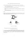
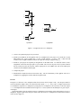
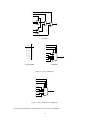
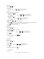
Laboratory Exercise 1
Switches, Lights, and Multiplexers
The purpose of this exercise is to learn how to connect simple input and output devices to an FPGA chip and
implement a circuit that uses these devices. We will use the switches SW 17−0 on the DE2 board as inputs to the
circuit. We will use light emitting diodes (LEDs) and 7-segment displays as output devices.
Part I
The DE2 board provides 18 toggle switches, called SW 17−0 , that can be used as inputs to a circuit, and 18 red
lights, called LEDR17−0 , that can be used to display output values. Figure 1 shows a simple VHDL entity that
uses these switches and shows their states on the LEDs. Since there are 18 switches and lights it is convenient
to represent them as arrays in the VHDL code, as shown. We have used a single assignment statement for all 18
LEDR outputs, which is equivalent to the individual assignments
LEDR(17) <= SW(17);
LEDR(16) <= SW(16);
...
LEDR(0) <= SW(0);
The DE2 board has hardwired connections between its FPGA chip and the switches and lights. To use SW 17−0 and
LEDR17−0 it is necessary to include in your Quartus II project the correct pin assignments, which are given in the
DE2 User Manual. For example, the manual specifies that SW 0 is connected to the FPGA pin N25 and LEDR 0 is
connected to pin AE23. A good way to make the required pin assignments is to import into the Quartus II software
the file called DE2 pin assignments.csv, which is provided on the DE2 System CD and in the University Program
section of Altera’s web site. The procedure for making pin assignments is described in the tutorial Quartus II
Introduction using VHDL Design, which is also available from Altera.
It is important to realize that the pin assignments in the DE2 pin assignments.csv file are useful only if the
pin names given in the file are exactly the same as the port names used in your VHDL entity. The file uses the
names SW[0] . . . SW[17] and LEDR[0] . . . LEDR[17] for the switches and lights, which is the reason we used
these names in Figure 1 (note that the Quartus II software uses [ ] square brackets for array elements, while the
VHDL syntax uses ( ) round brackets).
LIBRARY ieee;
USE ieee.std logic 1164.all;
- - Simple module that connects the SW switches to the LEDR lights
ENTITY part1 IS
PORT ( SW : IN
STD LOGIC VECTOR(17 DOWNTO 0);
LEDR : OUT STD LOGIC VECTOR(17 DOWNTO 0)); - - red LEDs
END part1;
ARCHITECTURE Behavior OF part1 IS
BEGIN
LEDR <= SW;
END Behavior
1
Figure 1. VHDL code that uses the DE2 board switches and lights.
Perform the following steps to implement a circuit corresponding to the code in Figure 1 on the DE2 board.
1. Create a new Quartus II project for your circuit. Select Cyclone II EP2C35F672C6 as the target chip, which
is the FPGA chip on the Altera DE2 board.
2. Create a VHDL entity for the code in Figure 1 and include it in your project.
3. Include in your project the required pin assignments for the DE2 board, as discussed above. Compile the
project.
4. Download the compiled circuit into the FPGA chip. Test the functionality of the circuit by toggling the
switches and observing the LEDs.
Part II
Figure 2a shows a sum-of-products circuit that implements a 2-to-1 multiplexer with a select input s. If s = 0 the
multiplexer’s output m is equal to the input x, and if s = 1 the output is equal to y. Part b of the figure gives a
truth table for this multiplexer, and part c shows its circuit symbol.
x
m
s
y
a) Circuit
s
s
m
0
1
x
y
x
y
b) Truth table
0
1
m
c) Symbol
Figure 2. A 2-to-1 multiplexer.
The multiplexer can be described by the following VHDL statement:
m <= (NOT (s) AND x) OR (s AND y);
You are to write a VHDL entity that includes eight assignment statements like the one shown above to describe
the circuit given in Figure 3a. This circuit has two eight-bit inputs, X and Y , and produces the eight-bit output M .
If s = 0 then M = X, while if s = 1 then M = Y . We refer to this circuit as an eight-bit wide 2-to-1 multiplexer.
It has the circuit symbol shown in Figure 3b, in which X, Y , and M are depicted as eight-bit wires. Perform the
steps shown below.
2
s
x7
y7
0
x6
y6
0
1
1
m7
m6
s
X
Y
x0
y0
0
1
8
0
8
M
1
8
m0
a) Circuit
b) Symbol
Figure 3. An eight-bit wide 2-to-1 multiplexer.
1. Create a new Quartus II project for your circuit.
2. Include your VHDL file for the eight-bit wide 2-to-1 multiplexer in your project. Use switch SW 17 on the
DE2 board as the s input, switches SW 7−0 as the X input and SW 15−8 as the Y input. Connect the SW
switches to the red lights LEDR and connect the output M to the green lights LEDG 7−0 .
3. Include in your project the required pin assignments for the DE2 board. As discussed in Part I, these
assignments ensure that the input ports of your VHDL code will use the pins on the Cyclone II FPGA
that are connected to the SW switches, and the output ports of your VHDL code will use the FPGA pins
connected to the LEDR and LEDG lights.
4. Compile the project.
5. Download the compiled circuit into the FPGA chip. Test the functionality of the eight-bit wide 2-to-1
multiplexer by toggling the switches and observing the LEDs.
Part III
In Figure 2 we showed a 2-to-1 multiplexer that selects between the two inputs x and y. For this part consider a
circuit in which the output m has to be selected from five inputs u, v, w, x, and y. Part a of Figure 4 shows how
we can build the required 5-to-1 multiplexer by using four 2-to-1 multiplexers. The circuit uses a 3-bit select input
s2 s1 s0 and implements the truth table shown in Figure 4b. A circuit symbol for this multiplexer is given in part c
of the figure.
Recall from Figure 3 that an eight-bit wide 2-to-1 multiplexer can be built by using eight instances of a 2-to-1
multiplexer. Figure 5 applies this concept to define a three-bit wide 5-to-1 multiplexer. It contains three instances
of the circuit in Figure 4a.
3
s2
s1
s0
u
v
0
0
1
w
x
1
0
m
1
0
1
y
a) Circuit
s2 s1 s0
m
0
0
0
0
1
1
1
1
u
v
w
x
y
y
y
y
0
0
1
1
0
0
1
1
0
1
0
1
0
1
0
1
s2
s1
s0
u
v
000
001
010
011
100
w
x
y
b) Truth table
c) Symbol
Figure 4. A 5-to-1 multiplexer.
s2
s1
s0
U
3
3
V
W
X
Y
3
3
000
001
010
011
100
3
M
3
Figure 5. A three-bit wide 5-to-1 multiplexer.
Perform the following steps to implement the three-bit wide 5-to-1 multiplexer.
4
m
1. Create a new Quartus II project for your circuit.
2. Create a VHDL entity for the three-bit wide 5-to-1 multiplexer. Connect its select inputs to switches
SW17−15 , and use the remaining 15 switches SW 14−0 to provide the five 3-bit inputs U to Y . Connect
the SW switches to the red lights LEDR and connect the output M to the green lights LEDG 2−0 .
3. Include in your project the required pin assignments for the DE2 board. Compile the project.
4. Download the compiled circuit into the FPGA chip. Test the functionality of the three-bit wide 5-to-1
multiplexer by toggling the switches and observing the LEDs. Ensure that each of the inputs U to Y can be
properly selected as the output M .
Part IV
Figure 6 shows a 7-segment decoder module that has the three-bit input c 2 c1 c0 . This decoder produces seven
outputs that are used to display a character on a 7-segment display. Table 1 lists the characters that should be
displayed for each valuation of c 2 c1 c0 . To keep the design simple, only four characters are included in the table
(plus the ‘blank’ character, which is selected for codes 100 − 111).
The seven segments in the display are identified by the indices 0 to 6 shown in the figure. Each segment is
illuminated by driving it to the logic value 0. You are to write a VHDL entity that implements logic functions that
represent circuits needed to activate each of the seven segments. Use only simple VHDL assignment statements
in your code to specify each logic function using a Boolean expression.
0
c2
c1
c0
5
7-segment
decoder
6
4
2
3
Figure 6. A 7-segment decoder.
c2 c1 c0
Character
000
001
010
011
100
101
110
111
H
E
L
O
Table 1. Character codes.
Perform the following steps:
1. Create a new Quartus II project for your circuit.
5
1
2. Create a VHDL entity for the 7-segment decoder. Connect the c 2 c1 c0 inputs to switches SW2−0 , and connect
the outputs of the decoder to the HEX0 display on the DE2 board. The segments in this display are called
HEX00 , HEX01 , . . ., HEX06 , corresponding to Figure 6. You should declare the 7-bit port
HEX0 : OUT STD LOGIC VECTOR(0 TO 6);
in your VHDL code so that the names of these outputs match the corresponding names in the DE2 User
Manual and the DE2 pin assignments.csv file.
3. After making the required DE2 board pin assignments, compile the project.
4. Download the compiled circuit into the FPGA chip. Test the functionality of the circuit by toggling the
SW2−0 switches and observing the 7-segment display.
Part V
Consider the circuit shown in Figure 7. It uses a three-bit wide 5-to-1 multiplexer to enable the selection of five
characters that are displayed on a 7-segment display. Using the 7-segment decoder from Part IV this circuit can
display any of the characters H, E, L, O, and ‘blank’. The character codes are set according to Table 1 by using
the switches SW14−0 , and a specific character is selected for display by setting the switches SW 17−15 .
An outline of the VHDL code that represents this circuit is provided in Figure 8. Note that we have used the
circuits from Parts III and IV as subcircuits in this code. You are to extend the code in Figure 8 so that it uses
five 7-segment displays rather than just one. You will need to use five instances of each of the subcircuits. The
purpose of your circuit is to display any word on the five displays that is composed of the characters in Table 1,
and be able to rotate this word in a circular fashion across the displays when the switches SW 17−15 are toggled.
As an example, if the displayed word is HELLO, then your circuit should produce the output patterns illustrated
in Table 2.
SW 17
SW 16
SW 15
SW 14 – 12
3
SW 11 – 9
3
SW 8 – 6
3
SW 5 – 3
SW 2 – 0
3
0
000
001
010
011
100
7-segment
decoder
3
7
5
6
4
2
3
3
Figure 7. A circuit that can select and display one of five characters.
6
1
LIBRARY ieee;
USE ieee.std logic 1164.all;
ENTITY part5 IS
PORT ( SW : IN
HEX0 : OUT
END part5;
STD LOGIC VECTOR(17 DOWNTO 0);
STD LOGIC VECTOR(0 TO 6));
ARCHITECTURE Behavior OF part5 IS
COMPONENT mux 3bit 5to1
PORT ( S, U, V, W, X, Y : IN
STD LOGIC VECTOR(2 DOWNTO 0);
M
: OUT STD LOGIC VECTOR(2 DOWNTO 0));
END COMPONENT;
COMPONENT char 7seg
PORT ( C
: IN
STD LOGIC VECTOR(2 DOWNTO 0);
Display : OUT STD LOGIC VECTOR(0 TO 6));
END COMPONENT;
SIGNAL M : STD LOGIC VECTOR(2 DOWNTO 0);
BEGIN
M0: mux 3bit 5to1 PORT MAP (SW(17 DOWNTO 15), SW(14 DOWNTO 12), SW(11 DOWNTO 9),
SW(8 DOWNTO 6), SW(5 DOWNTO 3), SW(2 DOWNTO 0), M);
H0: char 7seg PORT MAP (M, HEX0);
END Behavior;
LIBRARY ieee;
USE ieee.std logic 1164.all;
- - implements a 3-bit wide 5-to-1 multiplexer
ENTITY mux 3bit 5to1 IS
PORT ( S, U, V, W, X, Y : IN
STD LOGIC VECTOR(2 DOWNTO 0);
M
: OUT STD LOGIC VECTOR(2 DOWNTO 0));
END mux 3bit 5to1;
ARCHITECTURE Behavior OF mux 3bit 5to1 IS
. . . code not shown
END Behavior;
LIBRARY ieee;
USE ieee.std logic 1164.all;
ENTITY char 7seg IS
PORT ( C
: IN
Display : OUT
END char 7seg;
STD LOGIC VECTOR(2 DOWNTO 0);
STD LOGIC VECTOR(0 TO 6));
ARCHITECTURE Behavior OF char 7seg IS
. . . code not shown
END Behavior;
Figure 8. VHDL code for the circuit in Figure 7.
7
SW17 SW16 SW15
Character pattern
000
001
010
011
100
H
E
L
L
O
E
L
L
O
H
L
L
O
H
E
L
O
H
E
L
O
H
E
L
L
Table 2. Rotating the word HELLO on five displays.
Perform the following steps.
1. Create a new Quartus II project for your circuit.
2. Include your VHDL entity in the Quartus II project. Connect the switches SW 17−15 to the select inputs of
each of the five instances of the three-bit wide 5-to-1 multiplexers. Also connect SW 14−0 to each instance
of the multiplexers as required to produce the patterns of characters shown in Table 2. Connect the outputs
of the five multiplexers to the 7-segment displays HEX4, HEX3, HEX2, HEX1, and HEX0.
3. Include the required pin assignments for the DE2 board for all switches, LEDs, and 7-segment displays.
Compile the project.
4. Download the compiled circuit into the FPGA chip. Test the functionality of the circuit by setting the proper
character codes on the switches SW 14−0 and then toggling SW 17−15 to observe the rotation of the characters.
Part VI
Extend your design from Part V so that is uses all eight 7-segment displays on the DE2 board. Your circuit should
be able to display words with five (or fewer) characters on the eight displays, and rotate the displayed word when
the switches SW17−15 are toggled. If the displayed word is HELLO, then your circuit should produce the patterns
shown in Table 3.
SW17 SW16 SW15
000
001
010
011
100
101
110
111
Character pattern
H
E
L
L
O
H
E
L
L
O
H
E
L
L
O
H
E
L
L
O
E
L
L
O
H
L
L
O
H
E
L
O
H
E
L
O
H
E
L
L
Table 3. Rotating the word HELLO on eight displays.
Perform the following steps:
1. Create a new Quartus II project for your circuit and select as the target chip the Cyclone II EP2C35F672C6.
8
2. Include your VHDL entity in the Quartus II project. Connect the switches SW 17−15 to the select inputs of
each instance of the multiplexers in your circuit. Also connect SW 14−0 to each instance of the multiplexers
as required to produce the patterns of characters shown in Table 3. (Hint: for some inputs of the multiplexers
you will want to select the ‘blank’ character.) Connect the outputs of your multiplexers to the 7-segment
displays HEX7, . . ., HEX0.
3. Include the required pin assignments for the DE2 board for all switches, LEDs, and 7-segment displays.
Compile the project.
4. Download the compiled circuit into the FPGA chip. Test the functionality of the circuit by setting the proper
character codes on the switches SW 14−0 and then toggling SW 17−15 to observe the rotation of the characters.
c
Copyright 2006
Altera Corporation.
9