1
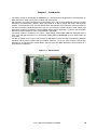
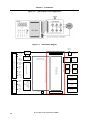
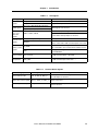
User’s Manual
Motor Control I/O Board
MC-IO Board For NEC Electronics Microcontrollers
Document No. U17857EU1V1UME0
Date Published August 2006
© NEC Electronics Corporation 2006
Printed in Germany
CAUTION
This is a Test- and Measurement equipment with possibility to be
significantly altered by user through hardware enhancements/modifications
and/or test or application software. Thus, with respect to Council Directive
89/336/EEC (Directive on compliance with the EMC protection
requirements), this equipment has no autonomous function. Consequently
this equipment is not marked by the CE-symbol.
EEDT-ST-0005-10
Redemption of Waste Electrical and Electronic Equipment
(WEEE) in accordance with legal regulations applicable in
the European Union only: This equipment (including all
accessories) is not intended for household use. After use
the equipment cannot be disposed of as household waste.
NEC Electronics (Europe) GmbH offers to take back the
equipment. All you need to do is register at
www.eu.necel.com/weee.
All (other) product, brand, or trade names used in this pamphlet are the trademarks or
registered trademarks of their respective owners.
Product specifications are subject to change without notice. To ensure that you have
the latest product data, please contact your local NEC Electronics sales office.
2
User’s Manual U17857EU1V1UME0
NOTES FOR CMOS DEVICES
1
VOLTAGE APPLICATION WAVEFORM AT INPUT PIN
Waveform distortion due to input noise or a reflected wave may cause malfunction. If the input of the
CMOS device stays in the area between VIL (MAX) and VIH (MIN) due to noise, etc., the device may
malfunction. Take care to prevent chattering noise from entering the device when the input level is fixed,
and also in the transition period when the input level passes through the area between VIL (MAX) and
VIH (MIN).
2
HANDLING OF UNUSED INPUT PINS
Unconnected CMOS device inputs can be cause of malfunction. If an input pin is unconnected, it is
possible that an internal input level may be generated due to noise, etc., causing malfunction. CMOS
devices behave differently than Bipolar or NMOS devices. Input levels of CMOS devices must be fixed
high or low by using pull-up or pull-down circuitry. Each unused pin should be connected to VDD or GND
via a resistor if there is a possibility that it will be an output pin. All handling related to unused pins must
be judged separately for each device and according to related specifications governing the device.
3
PRECAUTION AGAINST ESD
A strong electric field, when exposed to a MOS device, can cause destruction of the gate oxide and
ultimately degrade the device operation. Steps must be taken to stop generation of static electricity as
much as possible, and quickly dissipate it when it has occurred. Environmental control must be
adequate. When it is dry, a humidifier should be used. It is recommended to avoid using insulators that
easily build up static electricity. Semiconductor devices must be stored and transported in an anti-static
container, static shielding bag or conductive material. All test and measurement tools including work
benches and floors should be grounded. The operator should be grounded using a wrist strap.
Semiconductor devices must not be touched with bare hands. Similar precautions need to be taken for
PW boards with mounted semiconductor devices.
4
STATUS BEFORE INITIALIZATION
Power-on does not necessarily define the initial status of a MOS device. Immediately after the power
source is turned ON, devices with reset functions have not yet been initialized. Hence, power-on does
not guarantee output pin levels, I/O settings or contents of registers. A device is not initialized until the
reset signal is received. A reset operation must be executed immediately after power-on for devices
with reset functions.
5
POWER ON/OFF SEQUENCE
In the case of a device that uses different power supplies for the internal operation and external
interface, as a rule, switch on the external power supply after switching on the internal power supply.
When switching the power supply off, as a rule, switch off the external power supply and then the
internal power supply. Use of the reverse power on/off sequences may result in the application of an
overvoltage to the internal elements of the device, causing malfunction and degradation of internal
elements due to the passage of an abnormal current.
The correct power on/off sequence must be judged separately for each device and according to related
specifications governing the device.
6
INPUT OF SIGNAL DURING POWER OFF STATE
Do not input signals or an I/O pull-up power supply while the device is not powered. The current
injection that results from input of such a signal or I/O pull-up power supply may cause malfunction and
the abnormal current that passes in the device at this time may cause degradation of internal elements.
Input of signals during the power off state must be judged separately for each device and according to
related specifications governing the device.
User’s Manual U17857EU1V1UME0
3
• The information in this document is current as of August, 2006. The information is subject to
change without notice. For actual design-in, refer to the latest publications of NEC Electronics data
sheets or data books, etc., for the most up-to-date specifications of NEC Electronics products. Not
all products and/or types are available in every country. Please check with an NEC Electronics sales
representative for availability and additional information.
• No part of this document may be copied or reproduced in any form or by any means without the prior
written consent of NEC Electronics. NEC Electronics assumes no responsibility for any errors that may
appear in this document.
• NEC Electronics does not assume any liability for infringement of patents, copyrights or other intellectual
property rights of third parties by or arising from the use of NEC Electronics products listed in this document
or any other liability arising from the use of such products. No license, express, implied or otherwise, is
granted under any patents, copyrights or other intellectual property rights of NEC Electronics or others.
• Descriptions of circuits, software and other related information in this document are provided for illustrative
purposes in semiconductor product operation and application examples. The incorporation of these
circuits, software and information in the design of a customer's equipment shall be done under the full
responsibility of the customer. NEC Electronics assumes no responsibility for any losses incurred by
customers or third parties arising from the use of these circuits, software and information.
• While NEC Electronics endeavors to enhance the quality, reliability and safety of NEC Electronics products,
customers agree and acknowledge that the possibility of defects thereof cannot be eliminated entirely. To
minimize risks of damage to property or injury (including death) to persons arising from defects in NEC
Electronics products, customers must incorporate sufficient safety measures in their design, such as
redundancy, fire-containment and anti-failure features.
• NEC Electronics products are classified into the following three quality grades: "Standard", "Special" and
"Specific".
The "Specific" quality grade applies only to NEC Electronics products developed based on a customerdesignated "quality assurance program" for a specific application. The recommended applications of an NEC
Electronics product depend on its quality grade, as indicated below. Customers must check the quality grade of
each NEC Electronics product before using it in a particular application.
"Standard": Computers, office equipment, communications equipment, test and measurement equipment, audio
and visual equipment, home electronic appliances, machine tools, personal electronic equipment
and industrial robots.
"Special": Transportation equipment (automobiles, trains, ships, etc.), traffic control systems, anti-disaster
systems, anti-crime systems, safety equipment and medical equipment (not specifically designed
for life support).
"Specific": Aircraft, aerospace equipment, submersible repeaters, nuclear reactor control systems, life
support systems and medical equipment for life support, etc.
The quality grade of NEC Electronics products is "Standard" unless otherwise expressly specified in NEC
Electronics data sheets or data books, etc. If customers wish to use NEC Electronics products in applications
not intended by NEC Electronics, they must contact an NEC Electronics sales representative in advance to
determine NEC Electronics' willingness to support a given application.
(Note)
(1) "NEC Electronics" as used in this statement means NEC Electronics Corporation and also includes its
majority-owned subsidiaries.
(2) "NEC Electronics products" means any product developed or manufactured by or for NEC Electronics (as
defined above).
M8E 02. 11-1
4
User’s Manual U17857EU1V1UME0
For further information,
please contact:
NEC Electronics Corporation
1753, Shimonumabe, Nakahara-ku,
Kawasaki, Kanagawa 211-8668,
Japan
Tel: 044-435-5111
http://www.necel.com/
[America]
[Europe]
[Asia & Oceania]
NEC Electronics America, Inc.
2880 Scott Blvd.
Santa Clara, CA 95050-2554, U.S.A.
Tel: 408-588-6000
800-366-9782
http://www.am.necel.com/
NEC Electronics (Europe) GmbH
Arcadiastrasse 10
40472 Düsseldorf, Germany
Tel: 0211-65030
http://www.eu.necel.com/
NEC Electronics (China) Co., Ltd
7th Floor, Quantum Plaza, No. 27 ZhiChunLu Haidian
District, Beijing 100083, P.R.China
Tel: 010-8235-1155
http://www.cn.necel.com/
Hanover Office
Podbielskistrasse 166 B
30177 Hannover
Tel: 0 511 33 40 2-0
Munich Office
Werner-Eckert-Strasse 9
81829 München
Tel: 0 89 92 10 03-0
Stuttgart Office
Industriestrasse 3
70565 Stuttgart
Tel: 0 711 99 01 0-0
United Kingdom Branch
Cygnus House, Sunrise Parkway
Linford Wood, Milton Keynes
MK14 6NP, U.K.
Tel: 01908-691-133
Succursale Française
9, rue Paul Dautier, B.P. 52180
78142 Velizy-Villacoublay Cédex
France
Tel: 01-3067-5800
Sucursal en España
Juan Esplandiu, 15
28007 Madrid, Spain
Tel: 091-504-2787
NEC Electronics Shanghai Ltd.
Room 2509-2510, Bank of China Tower,
200 Yincheng Road Central,
Pudong New Area, Shanghai P.R. China P.C:200120
Tel: 021-5888-5400
http://www.cn.necel.com/
NEC Electronics Hong Kong Ltd.
12/F., Cityplaza 4,
12 Taikoo Wan Road, Hong Kong
Tel: 2886-9318
http://www.hk.necel.com/
Seoul Branch
11F., Samik Lavied’or Bldg., 720-2,
Yeoksam-Dong, Kangnam-Ku,
Seoul, 135-080, Korea
Tel: 02-558-3737
NEC Electronics Taiwan Ltd.
7F, No. 363 Fu Shing North Road
Taipei, Taiwan, R. O. C.
Tel: 02-8175-9600
http://www.tw.necel.com/
NEC Electronics Singapore Pte. Ltd.
238A Thomson Road,
#12-08 Novena Square,
Singapore 307684
Tel: 6253-8311
http://www.sg.necel.com/
Tyskland Filial
Täby Centrum
Entrance S (7th floor)
18322 Täby, Sweden
Tel: 08 638 72 00
Filiale Italiana
Via Fabio Filzi, 25/A
20124 Milano, Italy
Tel: 02-667541
Branch The Netherlands
Steijgerweg 6
5616 HS Eindhoven
The Netherlands
Tel: 040 265 40 10
G06.8A
User’s Manual U17857EU1V1UME0
5
[MEMO]
6
User’s Manual U17857EU1V1UME0
Preface
Readers
This manual is intented for users who want to understand the functions of the
Motor Control IO Board for NEC Electronics Microcontrollers.
Purpose
This manual presents the hardware manual of the Motor Control IO Board for
NEC Electronics Microcontrollers.
Organization
This system specification describes the following sections:
Legend
•
Inverter module
•
IGBT module
•
Opto isolation
•
Power supplies
•
User connections
Symbols and notation are used as follows:
Weight in data notation : Left is high-order column, right is low order column
Active low notation
: xxx (pin or signal name is over-scored) or
/xxx (slash before signal name)
Memory map address: : High order at high stage and low order at low stage
Note
: Explanation of (Note) in the text
Caution
: Item deserving extra attention
Remark
: Supplementary explanation to the text
Numeric notation
: Binary... XXXX or XXXB
Decimal... XXXX
Hexadecimal... XXXXH or 0x XXXX
Prefixes representing powers of 2 (address space, memory capacity)
K (kilo): 210 = 1024
M (mega): 220 = 10242 = 1,048,576
G (giga): 230 = 10243 = 1,073,741,824
User’s Manual U17857EU1V1UME0
7
8
User’s Manual U17857EU1V1UME0
Table of Contents
Preface . . . . . . . . . . . . . . . . . . . . . . . . . . . . . . . . . . . . . . . . . . . . . . . . . . . . . . . 7
Chapter 1
Introduction. . . . . . . . . . . . . . . . . . . . . . . . . . . . . . . . . . . . . . . . . . . . . . . . . . . 15
Chapter 2
System Specifications . . . . . . . . . . . . . . . . . . . . . . . . . . . . . . . . . . . . . . . . . . 18
Chapter 3
Hardware . . . . . . . . . . . . . . . . . . . . . . . . . . . . . . . . . . . . . . . . . . . . . . . . . . . . . 19
3.1
3.2
Operation . . . . . . . . . . . . . . . . . . . . . . . . . . . . . . . . . . . . . . . . . . . . . . . . . . . . . . . . . . . . 20
On-Board Components . . . . . . . . . . . . . . . . . . . . . . . . . . . . . . . . . . . . . . . . . . . . . . . . . 20
3.2.1
J4 - 40-Pin Ribbon Cable . . . . . . . . . . . . . . . . . . . . . . . . . . . . . . . . . . . . . . . . . . 20
3.2.2
14-Pin Terminal Block. . . . . . . . . . . . . . . . . . . . . . . . . . . . . . . . . . . . . . . . . . . . . 21
3.2.3
Speed Adjustment Potentiometer . . . . . . . . . . . . . . . . . . . . . . . . . . . . . . . . . . . . 23
3.2.4
Push button Switches . . . . . . . . . . . . . . . . . . . . . . . . . . . . . . . . . . . . . . . . . . . . . 23
3.3
Jumper Settings . . . . . . . . . . . . . . . . . . . . . . . . . . . . . . . . . . . . . . . . . . . . . . . . . . . . . . . 23
3.3.1
JP1–JP3 and JP6–JP . . . . . . . . . . . . . . . . . . . . . . . . . . . . . . . . . . . . . . . . . . . . . 23
3.3.2
Power Supply Jumper Selections . . . . . . . . . . . . . . . . . . . . . . . . . . . . . . . . . . . . 24
3.3.3
JP5 - VCC 5 V Selection. . . . . . . . . . . . . . . . . . . . . . . . . . . . . . . . . . . . . . . . . . . 25
3.3.4
JP11 - VCC 15 V Selection. . . . . . . . . . . . . . . . . . . . . . . . . . . . . . . . . . . . . . . . . 25
Chapter 4
4.1
4.2
4.3
Micro-Board and Power Module . . . . . . . . . . . . . . . . . . . . . . . . . . . . . . . . . . 26
Interface with Micro-Board . . . . . . . . . . . . . . . . . . . . . . . . . . . . . . . . . . . . . . . . . . . . . . 26
Interface with Power Module . . . . . . . . . . . . . . . . . . . . . . . . . . . . . . . . . . . . . . . . . . . . 26
Interface with Motor Unit Sensors . . . . . . . . . . . . . . . . . . . . . . . . . . . . . . . . . . . . . . . . 26
User’s Manual U17857EU1V1UME0
9
10
User’s Manual U17857EU1V1UME0
List of Figures
Figure 1-1:
Figure 1-2:
Figure 1-3:
Figure 3-1:
Figure 3-2:
Figure 3-3:
Figure 3-4:
Figure 3-5:
Figure 3-6:
Figure 3-7:
Figure 3-8:
Figure 3-9:
Figure 4-1:
MC-IO Board ............................................................................................................... 15
Typical Motor Control Application................................................................................ 16
Board Block Diagram .................................................................................................. 16
Physical Placement of Components on MC-IO Board................................................. 19
Pin Configuration ......................................................................................................... 20
Terminal Block Pin Configuration ................................................................................ 21
Signal Positions on the Terminal Block ....................................................................... 21
RS-232 Transceiver and Optional DB9 Connector...................................................... 22
Four-Digit, Seven-Segment LED ................................................................................. 22
Jumper Configurations ................................................................................................ 23
JP5, TF1 Configuration ............................................................................................... 25
JP11 Configuration ...................................................................................................... 25
Micro-Board and Power Module Block Diagram.......................................................... 26
User’s Manual U17857EU1V1UME0
11
12
User’s Manual U17857EU1V1UME0
List of Tables
Table 1-1:
Table 1-2:
Table 3-1:
Table 3-2:
Table 3-3:
Table 3-4:
Table 3-5:
Pin Signals...................................................................................................................... 17
Terminal Block Signals ................................................................................................... 17
Factory Settings.............................................................................................................. 19
JP Settings ..................................................................................................................... 24
JP1 Settings ................................................................................................................... 24
JP5, TF1 Settings ........................................................................................................... 25
JP11 Settings ................................................................................................................. 25
User’s Manual U17857EU1V1UME0
13
14
User’s Manual U17857EU1V1UME0
Chapter 1 Introduction
The motor control I/O board (MC-IO-GENERAL) is a board interface designed to be used between an
NEC Electronics motor control power module and micro-board.
Micro-boards are used to demonstrate and evaluate CPU and on-chip peripheral functions of NEC
Electronics microcontrollers (MCUs). When connected to an MC-IO board and motor control power
module, a micro-board can be used to demonstrate and evaluate CPU and motor control functions of
the NEC Electronics MCUs designed for 3-phase asynchronous current induction motor (ASIC) and
permanent magnet asynchronous current (PMAC) motor control applications. (Contact your local NEC
Electronics representative for a list of micro-boards supported.)
The power module is available in two types: a high-voltage module (MC-PWR-HV) designed to drive
100-, 120- and 220-volt motors or a low-voltage module (MC-LV-INVERTER) that can drive motors up
to 24 volts.
The MC-IO board serves as the user interface for operational control and signal conditioning between
the MCU and the power module. With this modular approach, a user can easily evaluate several NEC
Electronic 8- and 32-bit motor control MCUs. (Contact your local NEC Electronics representative for a
list of devices supported.)
Figure 1-1:
MC-IO Board
User’s Manual U17857EU1V1UME0
15
Chapter 1
Figure 1-2:
Introduction
Typical Motor Control Application
Figure 1-3:
Board Block Diagram
FRIWO
15V/2A
DB9 Male
Right-Angle
FX8C-100P-SV6
VCC_5V
Pwr-Jack
TRIP
16
Encoder
ENC_x
HALL_x
Sensor
Input
TEMP
Input to
ANI3
CMPx
HALL_x
Phase_x Voltage
M\Jumper Select Array
14-Pin Terminal Block
Phase_x
Voltage
V-U/V/W
PB
Switch
FORWARD
I_TRIP
PB
Switch
PB
Switch
REVERSE
I-Sense
Input to
ANIx
START/STOP
B-EMF
Comparator
CMPx
SPEED
Adjust
(TrimPot)
Voltage
Regulator
MODE
User Prototype Area
12-Rows -by- 24-Pins
CPU-I/O Pin-Array
All CPU-I/O Signals
RS232
Transceiver
Micro-Board Connection to MC-I/O Board (Outlined with Red)
PWM (6)
High-Side
Low-Side
CPU-I/O Signal Buffers
40-Pin Ribbon Cable Header
VCC_15V
PB
Switch
7_SEG
LED-1
7_SEG
LED-2
7_SEG
LED-3
7_SEG
LED-4
Reset
FX8C-100P-SV6
User’s Manual U17857EU1V1UME0
Chapter 1 Introduction
Table 1-1:
Type
Pin Signals
Names
Description
System power VCC_15 V
signals
VCC_5 V
PWM signals
Back-EMF
zero-cross
detection
signals
Power input to the MC-IO board
Regulated 5 V power
HI_U, HI_V, HIW (high-side FET drive)
LO_U, LO_V, LO_W (low-side FET drive)
Back-EMF comparator signals from power module
CMPU, CMPV, CMPW
Connected to interrupt inputs of the CPU
ANI0_IU, ANI1_IV, ANI2_IW
Current sense
signals
ISHUNT
Safety control
signals
Phase voltage
PWM signals from the CPU
Motor phase current; low-side current detect
Motor common shunt current; low-side current
detect; connected to A/D converter inputs of the CPU
PX_ITRIP
Over-current detection signal from the power module; connected to port x of the CPU for further action
TRIP
CPU-generated signal that turns off power to the
power MOSFET
V-U, V-V, V-W
Motor phase voltage monitoring signals; connected
to A/D converter inputs of the CPU
Power module
ANI7_TMP
temperature
Power module temperature sense signal; connected
to A/D converter input of the CPU
Table 1-2:
Category
Motor shaft encoder
Terminal Block Signals
Signal Names
ENC_A, ENC_B, ENC_Z
Description
Motor speed and direction signals; connected to
encoder inputs of the CPU
HALL effect sensor signal HALL_1, HALL_2, HALL_3
HALL effect sensor input; connected to interrupt
inputs of the CPU
Motor temperature input
Motor temperature input; connected to A/D converter
input of the CPU
ANI3_TEMP
User’s Manual U17857EU1V1UME0
17
Chapter 2 System Specifications
The MC-IO board has on-board user interface hardware for controlling and operating motor units.
•
15 V system power at power input (voltage regulator is used to generate VCC = 5 V)
•
Two 100-pin FX8C-100P-SV6 connectors for connecting a micro-board with motor control MCU to
the MC-IO board
•
40-pin ribbon cable that carries signals to and from the motor control power module
•
14-pin terminal block to connect sensor signals from the motor unit in use
•
Potentiometer connected to ANI4 input of the CPU to adjust speed
•
Push button switches that can be reprogrammed by the user
-
START/STOP
MODE
FORWARD
REVERSE
•
Four-digit, seven-segment light-emitting diode (LED) to display motor speed in revolutions per
minute (RPM) and other status information
•
RS-232 transceiver and optional DB9 connector (connected to a UART of the selected CPU)
•
User prototype area
- Twelve rows of 24-pin, 100-mil centered pin array for user prototyping
- Required CPU signals connected to CPU I/O pin array
- Board size of 3.5 (W) × 5.5 (L) inches
18
User’s Manual U17857EU1V1UME0
Chapter 3 Hardware
Figure 3-1:
Physical Placement of Components on MC-IO Board
Table 3-1:
Jumper
Setting
Factory Settings
Function
Description
JP1
1–2
INTP1_PX to JP6.2
Sensor inputs to INTP1
JP2
1–2
INTP2_PY to JP7.2
Sensor inputs to INTP2
JP3
1–2
INTP3_PZ to JP8.2
Sensor inputs to INTP3
JP4
Not used
JP5
1–2
Voltage regulator output = VCC_IS
JP6
1–2
CMPU_IS to JP6.2
JP7
1–2
CMPV_IS to JP7.2
JP8
1–2
CMPW_IS to JP8.2
JP9
Open
Transmit and receive loop-back
JP10
Open
RTS and CTS loop-back
JP11
1–2
System power supplied by MC-IO board, not power module
B-EMF comparator output
User’s Manual U17857EU1V1UME0
19
Chapter 3
Hardware
3.1 Operation
When connected to a micro-board and power module to drive the selected motor, the MC-IO board can
be used to demonstrate a selected CPU's motor control functions.
The unit can operate in standalone mode or be connected to a host computer through the MC-IO
board’s RS-232 port. In standalone mode, a user can control the motor from the MC-IO board’s push
buttons and speed potentiometer. To operate from a computer, special GUI software is needed.
(Contact your NEC Electronics representative for information.)
3.2 On-Board Components
3.2.1 J4 - 40-Pin Ribbon Cable
The 40-pin ribbon cable is used to connect motor control signals and motor position sensor signals
between the motor control power module and MC-IO board.
Figure 3-2:
Pin Configuration
ANI0_IU
1
2
PX_ITRIP
4
ANI6_SPARE
ANI1_IV
3
ANI2_IW
5
ANI5_ISHUNT
7
ANI7_TMP
9
VCC_5V
11
CMPU
13
CMPV
15
CMPW
17
TRIP
19
HI_U
21
HI_V
23
HI_W
25
LO_U
27
LO_V
29
LO_W
31
VCC_15V
33
V-U
35
V-V
37
V-W
39
GND_IS
SPARE_0
40
SPARE_1
Z5 Z5 Z5
GND_IS
Note: Clamped transient voltage suppressors (Zs) protect critical digital motor control signals.
20
User’s Manual U17857EU1V1UME0
Chapter 3
Hardware
3.2.2 14-Pin Terminal Block
The 14-pin terminal block is used for connecting motor sensor signals to the MC-IO board.
Figure 3-3:
Terminal Block Pin Configuration
J5
VCC_IS
1
8
ANI3_TEMP
GND_IS
2
9
GND_IS
ENC_Z
3
10
ENC_B
VCC_IS
4
11
ENC_A
GND_IS
5
12
GND_IS
VCC_IS
6
13
HALL1
HALL3
7
14
HALL2
Z5 Z5 Z5 Z5 Z5
Z5 Z5
GND_IS
GND_IS
Note: Clamped transient voltage suppressors (Zs) protect critical digital motor control signals.
Figure 3-4:
8
Signal Positions on the Terminal Block
9
10
11
TEMP
GND ENC_B
ENC_A
VCC
GND ENC_Z
VCC
1
2
3
4
12
13
14
GND HALL1
HALL2
GND
VCC
HALL3
5
6
7
16.3mm or
0.64-Inches
26.67mm or 1.05-Inches
User’s Manual U17857EU1V1UME0
21
Chapter 3
Figure 3-5:
Hardware
RS-232 Transceiver and Optional DB9 Connector
VCC_IS
16
3
+
RS232_TXD
RS232_RTS
RS232_RXD
RS232_CTS
Jumper
5
V+
V-
C1-
2
+
C3=1uF
6
C2+ MAX232CWE
16-Pin SOIC
C2- (300-Mil Body)
+
GND
C4=1uF Loopback
Jumper
Jumpers: Footprint Only
11
14 TXD_BD9
3
1
10
7
RTS_DB9
7
6
12
13 RXD_DB9
2
9
8
8
1M-742-8P
Loopback
Remark:
4
C1+
CTS_DB9
15
GND_IS
GND
GND_IS
5
Case
Z5 Z5 Z 5 Z5
1M-742-8P
4
Solder Blob
C2=1uF
1
DB9-M-RT
Footprint Only
C1=1uF
+
GND_IS
GND_IS
RS232_TXD and RS232_RXD: Transmit and receive signals of CPU
RS232_RTS and RS232_CTS: Port signals of CPU
Figure 3-6:
Micro-Board
100-Pin Connector Carrying CPU-Signals
CPU
MC-I/O Board
8-Bit DATA
PORT_x
PORT_x
Four-Digit, Seven-Segment LED
8-Bit
Latch
LD
8-Bit
Latch
LD
8-Bit
Latch
LD
8-Bit
Latch
LD
LD: Load DATA into Latch
7-Segment
Display
7-Segment
Display
7-Segment
Display
7-Segment
Display
The 7-segment LED data is latched one digit at a time. The ports used for the data and Latch Enable
(LD) signal differs from CPU to CPU, depending on the micro-board used. Refer to the associated
user's manual to determine which ports to use for the 7-segment LED.
22
User’s Manual U17857EU1V1UME0
Chapter 3
Hardware
3.2.3 Speed Adjustment Potentiometer
A 10 kΩ-potentiometer is connected to ANI4 of the analog-to-digital (A/D) converter input of CPU.
3.2.4 Push button Switches
There are four push button switches for motor control operation:
• START/STOP
• MODE
• FORWARD
• REVERSE
Push button functions can be reprogrammed by the user. In addition, there is a push button switch for
RESET.
3.3 Jumper Settings
3.3.1 JP1–JP3 and JP6–JP
The settings of JP6–JP8 select back-EMF zero-cross detection signals or phase-voltage signals. By
default, JP6–JP8 are configured to select the back-EMF detection signals. The phase-voltage signals
are analog signals that are reserved for future use.
The setting of JP1–JP2 select back-EMF zero-cross or HALL sensor signals for BLDC rotor position
detection. The outputs of the selected signals are connected to interrupt inputs of CPU.
Figure 3-7:
Jumper Configurations
JP6
JP7
JP1
1
CMPU_IS
2
CMPV_IS
1
2
3
2
V-U
JP2
1
3
INTP1_PX
2
V-V
3
1
HALL1_IS
INTP2_PY
3
HALL2_IS
JP8
JP3
1
CMPW_IS
2
1
3
2
V-W
INTP_PZ
3
HALL3_IS
User’s Manual U17857EU1V1UME0
23
Chapter 3
Table 3-2:
Setting
Hardware
JP Settings
Selected Power Source
Status
JP6.1 to JP6.2
CMPU_IS as sensor input
Default
JP6.3 to JP6.2
Phase voltage V-U
Future use
JP7.1 to JP7.2
CMPV_IS as sensor input
Default
JP7.3 to JP7.2
Phase voltage V-V
Future use
JP8.1 to JP8.2
CMPW_IS as sensor input
Default
JP8.3 to JP8.2
Phase voltage V-W
Future use
Table 3-3:
Setting
JP1 Settings
Description
JP1.1 to JP1.2
JP6.2: output of JP6
JP1.3 to JP1.2
HALL1_IS as sensor input
JP2.1 to JP2.2
JP7.2: output of JP7
JP2.3 to JP2.2
HALL2_IS as sensor input
JP3.1 to JP3.2
JP8.2: output of JP8
JP3.3 to JP3.2
HALL3_IS as sensor input
Status
Default
Default
Default
3.3.2 Power Supply Jumper Selections
The MC-IO board can be powered from the 15-volt power supply through the J11 power jack or from the
power module by configuring jumper JP11. The 5-volt power for the digital circuits can be derived from
the on-board regulator or from the power module, as specified by the configuration of jumper JP5.
When used with the low-voltage power module, the MC-IO board can supply 15 volts and up to 2 A
power to the power module. A low-voltage, 12-volt brushless DC motor can be operated for limited
loads that require less than 2 A.
24
User’s Manual U17857EU1V1UME0
Chapter 3
Hardware
3.3.3 JP5 - VCC 5 V Selection
An option is provided to supply VCC_5 V to the power module by connecting a jumper between pin 3 of
the TF1 filter and pin 3 of JP5 when the JP4 1–2 jumpers are connected. The TF1 filter is installed on
the bottom of the MC-IO board. The power module also can supply 5 volts DC to the MC-IO module
when JP5 2–3 are connected.
Figure 3-8:
JP5, TF1 Configuration
JP5
From Vol tage Regulator
VCC_5 V
Table 3-4:
Setting
TF1
1
1
2
2
3
3
GND_IS
VCC_IS
JP5, TF1 Settings
Selected Power Source
Status
JP5–1 to JP5–2
Voltage regulator output to MC-IO board
Default
JP5–1 to JP5–2
and
JP5–3 to TF1–3
VCC_S (5 VDC) to power module
JP5–2 to JP5–3
VCC_5 V from power module (system is powered by power
module)
3.3.4 JP11 - VCC 15 V Selection
The MC-IO board can be powered from the power module by connecting JP11 2–4.
Figure 3-9:
From 15 V, 2A
Power Jack
JP11 Configuration
1
2
3
4
To Voltage Regulator
on M C-IO Board
VC C_15 V From
Power M odule
Table 3-5:
JP11 Setting
JP11 Settings
Selected Main Clock Source
1–2
3–4
Power input from the MC-IO board power jack
2–4
VCC_15 V from power module; system powered by power module
User’s Manual U17857EU1V1UME0
Status
25
Chapter 4 Micro-Board and Power Module
Micro-Board and Power Module Block Diagram
FRIWO 15V@2A
TrimPot
R52
Speed
SMD Components
LED3
Flash Programming
And Debugging Interface
I/O - Pins
LED1
LED2
J2 = FX8C-100P-SV6 Header
CPU
D78F0714
I/O - Pins
LED0
I/O - Pins
OCD-Header
SMD Components
16-Pin Header
Terminal
Block
Motor Unit
Signals
J5
P1 = FX8C-100S-SV5 Receptacle
Power
Jack
I/O - Pins
Micro-Board
Connected to MC-I/O Board from Top-side
J1 = FX8C-100P-SV6 Header
40-Pin
Shrouded Header
Power-Module
Signals
J4
Micro-Board
3.5 - Inches
Motor Control I/O Board
Push-Buttons
Figure 4-1:
P2 = FX8C-100S-SV5 Receptacle
5.5 - Inches
2 - Inches
4.1 Interface with Micro-Board
The micro-board with NEC Electronics MCU can be connected to the MC-IO board from the top,
through J1–P1 and J2–P2 connectors. All CPU signals are available for the MC-IO board.
4.2 Interface with Power Module
The MC-IO board and power module are connected through a 40-pin ribbon cable. The signals from the
power module are directed to the CPU through 100-pin connectors.
4.3 Interface with Motor Unit Sensors
J5 is used to connect motor sensor signals such as hall, motor temperature and shaft encoder to the
MC-IO and CPU boards.
26
User’s Manual U17857EU1V1UME0