1
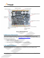
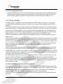
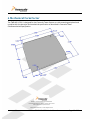
TWR‐MC‐LV3PH User’s Manual Rev. 1.0 Freescale Semiconductor Inc. Contents User’s Manual............................................................................................................................................................................... 1 1 Overview ...................................................................................................................................................... 3 2 Reference Documents .............................................................................................................................. 5 3 Hardware Features ................................................................................................................................... 5 3.1 Power Supply ........................................................................................................................................................................ 6 3.2 Electrical Characteristics ................................................................................................................................................. 6 3.3 Three Phase Field Effect Transistor Pre‐driver ..................................................................................................... 7 3.4 3‐Phase Bridge ..................................................................................................................................................................... 8 3.5 Bus Voltage and Current Feedback ............................................................................................................................. 8 3.6 Safety Functions .................................................................................................................................................................. 9 3.7 Back EMF Signals ................................................................................................................................................................ 9 3.8 Phase Current Sensing ...................................................................................................................................................... 9 3.9 LED Indication ................................................................................................................................................................... 10 3.10 Encoder / Hall‐Effect Interace ................................................................................................................................. 10 3.11 Brake .................................................................................................................................................................................. 10 4 Signal Description .................................................................................................................................. 11 4.1 Power Supply Input Connector J1 ............................................................................................................................. 11 4.2 External Brake Resistor Interface J4 ........................................................................................................................ 11 4.3 Motor Connector J5 ......................................................................................................................................................... 11 4.4 Encoder / Hall‐effect Interface J8 .............................................................................................................................. 11 4.5 Elevator Connections ..................................................................................................................................................... 12 5 Configuration Settings .......................................................................................................................... 17 5.1 Zero‐Ohm Resistors ........................................................................................................................................................ 17 5.2 Jumper Settings ................................................................................................................................................................ 17 6 Mechanical Form Factor ...................................................................................................................... 19 TWR‐MC‐LV3PH User’s Manual Page 2 of 19 1 Overview The 3‐phase Low Voltage Motor Control board (TWR‐MC‐LV3PH) is a peripheral Tower System Module with one of the available MCU tower module, accommodating a selected microcontroller, it provides a ready‐made, software‐development platform for one‐third horsepower off‐line motors. Feedback signals are provided that allow a variety of algorithms to control 3‐phase PMSM and BLDC motors. The TWR‐MC‐LV3PH module features: • Power supply voltage input 12‐24VDC, extended up to 50V ( see chapter 3.2 Electrical Characteristics for details) • Output current up to 8 Amps • Power supply reverse polarity protection circuitry • 3‐phase bridge inverter (6‐MOSFET’s) • 3‐phase MOSFET gate driver with over current and under voltage protection • 3‐phase and d.c. bus‐current‐sensing shunts • DC bus‐voltage sensing • 3‐phase back‐EMF voltage sensing circuitry • Low‐voltage on‐board power supplies • Encoder/Hall sensor sensing circuitry • Motor power and signal connectors • User LED, power‐on LED, 6 PWM LED diodes A block diagram for the TWR‐MC‐LV3PH is shown in the figure below. TWR‐MC‐LV3PH User’s Manual Page 3 of 19 Figure 1 ‐ TWR‐MC‐LV3PH Block Diagram TWR‐MC‐LV3PH User’s Manual Page 4 of 19 Figure 2 ‐ TWR‐MC‐LV3PH Image 2 Reference Documents The documents listed below should be referenced for more information on the Freescale Tower system and the TWR‐MC‐LV3PH. Refer to http://www.freescale.com/tower for the latest revision of all released Tower documentation. • TWR‐MC‐LV3PH Schematics • TWR‐MC‐LV3PH Quick Start Guide • Freescale MC33937A Three Phase Field Effect Transistor Pre‐driver 3 Hardware Features This section provides more details about the features and functionality of the TWR‐MC‐LV3PH. TWR‐MC‐LV3PH User’s Manual Page 5 of 19 3.1 Power Supply Freescale’s 3‐phase Low Voltage Motor Control Tower Module is a 3‐phase power stage that will operate off d.c. input voltages of 12 to 24 volts, 8 amps. The module contains reverse polarity protection circuitry. It is intended that the TWR‐MC‐LV3PH be powered from an external power supply of 12 to 24 volts, 4 to 8 amps depending on used motor. The module includes 5.0V and 3.3V supplies which are capable to provide power to entire Tower System. 3.1.1 +5V Power Supply The +5V level is generated by means of the LM2594HVM switching step‐down regulator (see TWR‐MC‐ LV3PH schematic), which generates this level from bus voltage. This converter can supply up to 500 mA. This voltage level serves the MC33269D linear regulator, encoder and optionally entire tower system. If the LM2594HVM converter operates properly, the D7 green LED is lit. 3.1.2 +3.3V Power Supply An important voltage level for this board is +3.3V. This voltage level is obtained from the MC33269D linear voltage regulator and can supply up to 800 mA. 3.1.3 +1.65V Voltage Reference Current sensing operational amplifiers use 1.65V voltage level connected to non‐inverted inputs. This level is obtained from a precision voltage reference LM4041 (D6). 3.1.4 Analog Power Supply and Grounding For analog quantities sensing (currents and voltages) is used separated analog voltage 3.3V and ground. This voltage level can be chosen from two sources. One is separated from 3.3V digital power supply using an LC filter and the second source is from the primary elevator port. A source selection is done via jumpers J2 and J3. 3.2 Electrical Characteristics The electrical characteristics in table below apply to operations at 25°C with a 24‐Vd.c. power‐ supply voltage. Input voltage maximal value can be higher than 24V. A 50V maximal input voltage value is allowed, but the DC bus and BEMF sensing circuits need to be modified. The divider resistors in these circuits need to be changed to increase sensing range up to 50V if required. It prevents scaled quantities exceeding the maximally allowed input voltage value on the controller input pins. If an input voltage higher than 24V is applied, the plugged TWR modules might be damaged. TWR‐MC‐LV3PH User’s Manual Page 6 of 19 Characteristic Symbol Min Typ Max Units DC input voltage Vdc 12 — 24 V Quiescent Current ICC — TBD — mA Logic 1 Input Voltage VIH 1.5 — 1.7 V Logic 0 Input Voltage VIL 0.9 — 1 V Input Resistance RIn — 10 — kΩ Analogue Output Range VOut 0 — 3.3 V Bus Current Sense Voltage ISense — 412 — mV/A Bus Current Sense Offset Ioffset Bus Voltage Sense Voltage* VBus Bus Voltage Sense Offset Voffset +1.65 — 91 V — 0 mV/V V Bus Continuous Output Current ** IC — — 8 A Total Power Dissipation (per MOSFET) *** PD — — TBD W Dead-time (set by SW MC33937) **** toff 0 — 15 us Table 1 ‐ Electrical Characteristics 3.3 Three Phase Field Effect Transistor Predriver The TWR‐MC‐LV3PH module utilizes Freescale MC33937A Three Phase Field Effect Transistor Pre‐ driver. The 33937 is a Field Effect Transistor (FET) pre‐driver designed for three phase motor control and similar applications. The integrated circuit (IC) uses SMARTMOS™ technology. The IC contains three High Side FET pre‐drivers and three Low Side FET pre‐drivers. Three external bootstrap capacitors provide gate charge to the High Side FETs. The IC interfaces to a MCU via six direct input control signals, an SPI port for device setup and asynchronous reset, enable and interrupt signals. Features: • Fully specified from 8.0V to 40V covers 12V and 24V automotive systems • Extended operating range from 6.0V to 58V covers 12V and 42V systems • Greater than 1.0A gate drive capability with protection • Protection against reverse charge injection from CGD and CGS of external FETs • Includes a charge pump to support full FET drive at low battery voltages • Dead time is programmable via the SPI port • Simultaneous output capability enabled via safe SPI command • MC33937A supports very high current loads TWR‐MC‐LV3PH User’s Manual Page 7 of 19 3.4 SPI communication Freescale MC33937A driver uses SPI communication for operating parameter, mode and interrupt setting. Driver command and registers are described in a driver manual. The selecction between two Chip Select signals is available on the board via two 0‐ohm resistors R95, R96 (see 5.1). 3.5 3Phase Bridge The output stage is configured as a 3‐phase bridge with MOSFET‐output transistors. It is simplified considerably by an integrated‐gate driver that has an over‐current, under voltage and other safety features. At the input, pull‐down resistor R26 sets logic low in the absence of a signal for the low side transistor. Open input pull‐down is important because the power transistors must stay off in the case of a broken connection or an absence of power on the daughter board. Gate driver inputs are 3.3V compatible. A Freescale device, an MC33937A, supplies the gate drive. The MC33937A also provides under voltage hold‐off and over‐current. Under voltage hold‐off threshold value is 8V. MC33937A has an implemented dead‐time insertion which can be configured using SPI. The default dead‐time value is typically 15μs. One important design decision in a motor drive is the selection of gate‐drive impedance for the output transistors. Resistor R14, R15, diode D8, and the MC33937A nominal 100mA current sinking capability determine gate‐drive impedance for the lower half‐bridge transistor. A similar network is used on the upper half‐bridge. These networks set the turn‐on gate drive impedance at approximately 100Ω and the turn‐off gate drive to approximately 100mA. These values produce transition times of approximately 285 ns. Transition times of this length represent a carefully weighed compromise between power dissipation and noise generation. Generally, transition times longer than 250 ns tend to get power hungry at non‐ audible PWM rates; transition times under 50 ns create di/dts so large that proper operation is difficult to achieve. The 3‐phase Low Voltage Motor Control Tower Module is designed with switching times at the higher end of this range to minimize noise. Anti‐parallel diode softness is also a primary design consideration. If the anti‐parallel diodes in an off‐ line motor drive are allowed to snap, the resulting di/dts can cause noise management problems difficult to solve. In general, the peak to zero di/dt should be approximately equal to the di/dt applied to turning off the anti‐parallel diodes. The IRFR540Z MOSFETs used in this design are targeted at this kind of reverse recovery. 3.6 Bus Voltage and Current Feedback Bus voltage is scaled down by a voltage divider consisting of R74, R77 and R79. The values are chosen such that a 36.3‐volt bus voltage corresponds to 3.3V at output V_SENSE_DCB. V_SENSE_DCB is scaled at 91mV per volt of the DC bus voltage and is terminated on the main elevator port. An additional output, V_SENSE_DCB_HALF, provides a reference used in zero‐crossing detection. V_SENSE_DCB_HALF is scaled at 45.5mV per volt of the DC bus voltage and is also terminated on the main port. TWR‐MC‐LV3PH User’s Manual Page 8 of 19 Bus current is sampled by resistor R10 and amplified in either the MC33937A’s operational amplifier or external operational amplifier U6B. This circuit provides a voltage output suitable for sampling on A/D (analogue‐to‐digital) inputs. Both operational amplifiers are connected as differential amplifiers for bus‐current sensing with the equal gain given by: A = R40/(R38+R39) The output voltage is shifted up by +1.65V_REF to accommodate positive and negative current swings. A ±400‐mV voltage drop across the sense resistor corresponds to a measured current range of ±8 amps. AMP_OUT signal is internally connected to the over current comparator of the MC33937A and provides an over‐current triggering function. The shunt resistor is represented by a 0.05‐ohm resistance WELWYN SMD precision resistor, the same as the phase current measurement resistors. 3.7 Safety Functions The MC33937A provides over‐current and under voltage functions. Bus current feedback is filtered to remove spikes, and this signal is fed into the MC33937A current comparator input ITRIP. Therefore, when bus current exceeds reference value (set by trimmer R37), all six output transistors are switched off. Once a fault state has been detected, all six gate drivers are off until the fault state is cleared in by the CLINT0 command or by switching the board off. Then you can switch the power stage on. The under voltage function is implemented internally. The MC33937A’s supply voltage is sensed internally. If this voltage is lower than 8V, the hold off circuit is evaluated and an interrupt is generated if set. The MC33927 safety functions keep the driver operating properly and within safe limits. Current limiting by itself, however, does not necessarily ensure that a board is operating within safe thermal limits. The MC33927 has a thermal warning feature. If the temperature rises above 170°C on one of the three detectors, then an interrupt is generated if set. The MC33927 driver has also other safety features such as desaturation detection, phase error, framing error, write error after the lock and exiting RST. All these features can be configured through SPI to trigger interrupts. Detail information is available in the driver datasheet. 3.8 Back EMF Signals Back EMF signals are included to support sensorless algorithms for brushless d.c. motors and dead time distortion correction for sinusoidal motors. The raw phase voltage is scaled down by a voltage divider consisting of R47 and R48 (phase A). Output from this divider produces back EMF sense voltage BEMF_SENSE_A. Resistor values are chosen such that a 36.3‐volt of phase voltage corresponds to a 3.3‐ volt A/D input. BEMF_SENSE_A is terminated to the elevator main port. 3.9 Phase Current Sensing Sampling resistors provide phase current information for all three phases. Because these resistors sample current in the lower phase legs, they do not directly measure phase current. However, given TWR‐MC‐LV3PH User’s Manual Page 9 of 19 phase voltages for all three phases, phase current can be constructed mathematically from the lower phase leg values. This information can be used in vector‐control algorithms for AC induction motors.. Referencing the sampling resistors to the negative motor rail makes the measurement circuitry straightforward and inexpensive. Current is sampled by resistor R7 (phase A) and amplified by the differential amplifier U5A. This circuit provides a voltage output suitable for sampling on A/D inputs. An AD8656 is used as a differential amplifier. With R38 = R41 and R39 = R42 and R40 = R46, the gain is given by: A = R40/(R39+R38) The input voltage is shifted up by +1.65V_REF to accommodate both positive and negative current swings. A ±400‐mV voltage drop across the shunt resistor corresponds to a measured current range of ±8 amps. As a source for +1.65V_REF, a precision shunt voltage reference LM4041. 3.10 LED Indication This module also contains 8 LEDs as indicators: • D5 — User LED diode for user defined purposes, activated on high level.. • D7 — Indicates that the +5V level is properly generated. • D14 ‐ PWM_AT indication LED, activated on low level. • D16 ‐ PWM_AB indication LED, activated on high level. • D18 ‐ PWM_BT indication LED, activated on low level. • D15 ‐ PWM_BB indication LED, activated on high level. • D17 ‐ PWM_CT indication LED, activated on low level. • D19 ‐ PWM_CB indication LED, activated on high level. 3.11 Encoder / HallEffect Interace The TWR‐MC‐LV3PH contains an Encoder/Hall‐Effect interface. The circuit is designed to accept +3.3V to +5.0V encoder or Hall‐Effect sensor inputs. Input noise filtering is supplied on the input path for the Encoder/Hall‐Effect interface. Filtered signals are then connected to the elevator main port. 3.12 Brake An external brake resistor can be connected to dissipate re‐generative motor energy during periods of active deceleration or rapid reversal. Under these conditions, motor back EMF adds to the dc bus voltage. Without a means to dissipate excess energy, an overvoltage condition could easily occur. With an external dissipative resistor connected to J4, it serves to dissipate energy across the dc bus. MOSEFET Q8 is turned on by software when the bus voltage sensing circuit exceeds level set in software. Power dissipation capability depends, of course, on the capability of the externally connected dissipative resistor. The MIC4127YME is a dual MOSFET pre‐driver 5.0V tolerant. This board uses its A channel to drive the braking resistance MOSFET. TWR‐MC‐LV3PH User’s Manual Page 10 of 19 4 Signal Description This section provides more details about signals of input / output connectors and jumpers of the TWR‐ TWR‐MC‐LV3PH. 4.1 Power Supply Input Connector J1 The power supply input connector, labeled J1, accepts d.c. voltages from 12V to 50V/ 8A max. The J1 connector is a 2.1mm power jack for plug‐in type DC power supply connections. The board has reverse polarity protection. Power applied to the board is indicated by a green color +5V LED . 4.2 External Brake Resistor Interface J4 A brake resistor can be connected to brake‐resistor connector J4. The brake resistor allows power dissipation and can be controlled through the Brake control signal. 4.3 Motor Connector J5 Power outputs to the motor are located on connector J1. Phase outputs are labeled A, B, and C. Table 2 contains pin assignments. On a permanent magnet synchronous motor, any one of the three phase windings can be connected here. For brushless d.c. motors, you must connect the wire colour coded for phase A into the connector terminal labeled A, and so on for phase B and phase C. 1 2 Signal Name A B 3 C Pin # Description Supplies power to motor phase A Supplies power to motor phase B Supplies power to motor phase C Table 2 – Motor Connector J5 – Signal Description 4.4 Encoder / Halleffect Interface J8 The Encoder/Hall‐Effect interface J8 is located on the right edge of the board. The circuit is designed to accept +3.3V to +5V encoder or Hall‐Effect sensor inputs. Input noise filtering is supplied on the input path to the Encoder/Hall‐Effect interface. Table 3 shows the Encoder/Hall‐Effect interface pin description. Pin # Signal Name 1 +5.0V Description Supplies power from the board to either ENCODER or Hall sensors TWR‐MC‐LV3PH User’s Manual Page 11 of 19 2 3 4 5 GND Phase A Phase B Phase C ENCODER or Hall sensors ground ENCODER or Hall Phase A input ENCODER or Hall Phase B input ENCODER or Hall Phase C input Table 3 – Encoder / Hall‐effect Interface J8 – Signal Description 4.5 Elevator Connections The TWR‐MC‐LV3PH features two expansion card‐edge connectors that interface to Elevator boards in a Tower System: the Primary and Secondary Elevator connectors. Table provides the pinout for the Primary and Secondary Elevator Connector. An “X” in the “Used” column indicated that there is a connection from the TWR‐MC‐LV3PH to that pin on the Elevator connector. An “X” in the “Jmp” column indicates that a jumper is available that can configure or isolate the connection from the Elevator connector. Table 4 ‐ TWR‐MC‐LV3PH Primary Elevator Connector Pinout TWR‐MC‐LV3PH Primary Connector Pin Name B1 5V Pin Name 5.0V Power B2 B3 B4 ELE_PS_SENSE B5 B6 Usage Used Jmp X A1 5V Used Jmp 5.0V Power GND Ground X A2 3.3V 3.3V Power X A3 Elevator Power Sense X GND Ground X Ground X B7 GND SDHC_CLK / SPI1_CLK B8 SDHC_D3 / SPI1_CS1_b X GND Ground X 3.3V 3.3V Power X A4 3.3V 3.3V Power X A5 GND Ground X A6 A7 GND SCL0 Ground X A8 SDA0 A9 GPIO9 / CTS1 GPIO8 / SDHC_D2 A10 B9 SDHC_D3 / SPI1_CS0_b B10 SDHC_CMD / SPI1_MOSI B11 B12 SDHC_D0 / SPI1_MISO ETH_COL B13 ETH_RXER B14 ETH_TXCLK B15 ETH_TXEN B16 ETH_TXER B17 B18 B19 Usage A11 A12 GPIO7 / SD_WP_DET ETH_CRS A13 ETH_MDC A14 ETH_MDIO A15 ETH_RXCLK A16 ETH_RXDV ETH_TXD3 A17 ETH_RXD3 ETH_TXD2 A18 ETH_RXD2 ETH_TXD1 A19 ETH_RXD1 B20 ETH_TXD0 A20 ETH_RXD0 B21 GPIO1 / RTS1 USER_LED X A21 SSI_MCLK B22 GPIO2 / SDHC_D1 BRAKE_CONTROL X A22 SSI_BCLK B23 GPIO3 A23 SSI_FS B24 CLKIN0 A24 SSI_RXD B25 CLKOUT1 A25 SSI_TXD B26 GND X A26 GND Ground X Ground TWR‐MC‐LV3PH User’s Manual Page 12 of 19 TWR‐MC‐LV3PH Primary Connector Pin Name AN7 B27 Usage Used Jmp Pin A27 AN6 I_SENCE_C / I_SENSE_DCB AN5 I_SENCE_A / V_SENSE_DCB_HALF AN4 V_SENSE_DCB B32 GND DAC1 Ground B33 TMR3 B34 B35 B36 B37 3.3V PWM7 3.3V Power B38 PWM6 B39 PWM5 PWM_CB B40 PWM4 PWM_CT B41 CANRX0 B42 CANTX0 B43 1WIRE B44 B45 B46 B28 B29 B30 B31 X X A28 X X A29 X X A30 Name AN3 AN2 AN1 AN0 Usage I_SENSE_C / BEMF_SENSE_C I_SENSE_B / BEMF_SENSE_B I_SENSE_A / BEMF_SENSE_A Used Jmp X X X X X X A31 A32 GND DAC0 Ground X A33 TMR1 ENC_PHASE_B X TMR2 ENC_INDEX X A34 TMR0 ENC_PHASE_A X GPIO4 A35 GPIO6 X A36 A37 3.3V PWM3 3.3V Power PWM_BB X X A38 PWM2 PWM_BT X X A39 PWM1 PWM_AB X X A40 PWM0 PWM_AT X A41 RXD0 A42 TXD0 A43 RXD1 SPI0_MISO (IO1) MISO X A44 TXD1 SPI0_MOSI (IO0) MOSI X A45 VSS GNDA_ELV X X SPI0_CS0_b /SS X A46 VDDA VDDA_ELV X X B47 SPI0_CS1_b /SS X A47 VREFA1 B48 SPI0_CLK SCLK X A48 VREFA2 B49 GND SCL1 Ground X GND A49 B50 A50 GPIO14 Ground X B51 SDA1 A51 GPIO15 B52 GPIO5 / SPI0_HOLD (IO3) DRV_EN A52 GPIO16 / SPI0_WP (IO2) A53 B54 A54 B55 USB0_DM_PDOWN IRQ_H GPIO17 USB0_DM USB0_DP_PDOWN X B53 A55 USB0_DP B56 IRQ_G A56 USB0_ID B57 IRQ_F A57 USB0_VBUS B58 IRQ_E A58 TMR7 B59 IRQ_D A59 TMR6 B60 IRQ_C A60 TMR5 B61 IRQ_B DRV_INT X A61 TMR4 B62 IRQ_A DRV_OC X X X A62 RSTIN_b B63 EBI_ALE / EBI_CS1_b A63 RSTOUT_b RESET X B64 EBI_CS0_b A64 CLKOUT0 B65 GND GND A66 EBI_AD14 Ground X A65 EBI_AD15 Ground X B66 B67 EBI_AD16 A67 EBI_AD13 B68 EBI_AD17 A68 EBI_AD12 B69 EBI_AD18 A69 EBI_AD11 TWR‐MC‐LV3PH User’s Manual Page 13 of 19 TWR‐MC‐LV3PH Primary Connector Pin B70 Name EBI_AD19 Usage Used Jmp Pin A70 A71 B71 EBI_R/W_b B72 EBI_OE_b B73 EBI_D7 B74 B75 EBI_AD10 Jmp EBI_AD9 EBI_AD8 A73 EBI_AD7 EBI_D6 EBI_D5 A74 EBI_AD6 A75 EBI_AD5 B76 EBI_D4 A76 EBI_AD4 B77 EBI_D3 B78 EBI_D2 A77 EBI_AD3 A78 EBI_AD2 B79 EBI_D1 EBI_AD1 B80 EBI_D0 A80 EBI_AD0 B81 GND Ground X B82 3.3V 3.3V Power X A81 GND Ground X A82 3.3V 3.3V Power X A72 A79 Name Usage TWR‐MC‐LV3PH User’s Manual Page 14 of 19 Used Table 5 ‐ TWR‐MC‐LV3PH Secondary Elevator Connector Pinout TWR‐SER2 Secondary Connector Pin Name D1 5V Jmp Pin Name D2 D3 C1 5V GND Ground X C2 3.3V C3 D4 ELE_PS_SENSE D5 GND Ground X D6 D7 GND SPI2_CLK Ground X D8 SPI2_CS1_b D9 SPI2_CS0_b D10 SPI2_MOSI D11 D12 SPI2_MISO ETH_COL Usage Used Jmp GND Ground X 3.3V C4 3.3V C5 GND Ground X C6 C7 GND SCL2 Ground X C8 SDA2 C9 GPIO25 C10 ULPI_STOP C11 C12 ULPI_CLK GPIO26 D13 ETH_RXER C13 ETH_MDC D14 ETH_TXCLK C14 ETH_MDIO D15 ETH_TXEN C15 ETH_RXCLK D16 GPIO18 C16 ETH_RXDV D17 GPIO19 / SDHC_D4 C17 GPIO27 / SDHC_D6 D18 GPIO20 / SDHC_D5 C18 GPIO28 / SDHC_D7 D19 ETH_TXD1 C19 ETH_RXD1 D20 ETH_TXD0 C20 ETH_RXD0 D21 ULPI_NEXT / USB1_DM C21 ULPI_DATA0 / USB3_DM D22 ULPI_DIR / USB1_DP C22 ULPI_DATA1 / USB3_DP D23 UPLI_DATA5 / USB2_DM C23 ULPI_DATA2 / USB4_DM D24 ULPI_DATA6 / USB2_DP C24 ULPI_DATA3 / USB4_DP D25 ULPI_DATA7 C25 ULPI_DATA4 D26 GND LCD_HSYNC / LCD_P24 Ground X C26 D27 C27 GND AN11 Ground X D28 LCD_VSYNC / LCD_P25 C28 AN10 D29 AN13 C29 AN9 D30 AN12 C30 AN8 D31 Ground X C31 D32 GND LCD_CLK / LCD_P26 C32 GND GPIO29 Ground X D33 TMR11 C33 TMR9 D34 TMR10 C34 TMR8 D35 GPIO21 C35 GPIO30 D36 C36 D37 3.3V PWM15 C37 3.3V PWM11 D38 PWM14 C38 PWM10 D39 PWM13 C39 PWM9 D40 PWM12 C40 PWM8 D41 CANRX1 C41 RXD2 / TSI0 D42 CANTX1 C42 TXD2 / TSI1 TWR‐MC‐LV3PH User’s Manual Page 15 of 19 TWR‐SER2 Secondary Connector Pin D43 Name GPIO22 Jmp Pin C43 C44 D44 LCD_OE / LCD_P27 D45 LCD_D0 / LCD_P0 D46 LCD_D1 / LCD_P1 D47 LCD_D2 / LCD_P2 D48 LCD_D3 / LCD_P3 D49 D50 GND GPIO23 Ground D51 GPIO24 D52 D53 D54 Name RTS2 / TSI2 Usage Used Jmp CTS2 / TSI3 RXD3 / TSI4 C46 TXD3 / TSI5 C47 RTS3 / TSI6 C48 CTS3 / TSI7 X C49 GND C50 LCD_D4 / LCD_P4 Ground X C51 LCD_D5 / LCD_P5 LCD_D12 / LCD_P12 C52 LCD_D6 / LCD_P6 LCD_D13 / LCD_P13 C53 C54 D55 LCD_D14 / LCD_P14 IRQ_P / SPI2_CS2_b LCD_D7 / LCD_P7 LCD_D8 / LCD_P8 C55 LCD_D9 / LCD_P9 D56 IRQ_O / SPI2_CS3_b C56 LCD_D10 / LCD_P10 D57 IRQ_N C57 LCD_D11 / LCD_P11 D58 IRQ_M C58 TMR16 D59 IRQ_L C59 TMR15 D60 IRQ_K C60 TMR14 D61 IRQ_J C61 TMR13 D62 IRQ_I C62 LCD_D15 / LCD_P15 D63 LCD_D18 / LCD_P18 C63 LCD_D16 / LCD_P16 D64 LCD_D19 / LCD_P19 C64 LCD_D17 / LCD_P17 C45 D65 GND X GND EBI_AD20 / LCD_P42 Ground C65 D66 C66 EBI_BE_32_24_b / LCD_P28 Ground X D67 EBI_AD21 / LCD_P43 C67 EBI_BE_23_16_b / LCD_P29 EBI_AD22 / LCD_P44 EBI_BE_15_8_b / LCD_P30 C69 EBI_BE_7_0_b / LCD_P31 D70 EBI_AD23 / LCD_P45 EBI_AD24 / LCD_P46 C70 EBI_TSIZE0 / LCD_P32 D71 EBI_AD25 / LCD_P47 C71 EBI_TSIZE1 / LCD_P33 D72 EBI_AD26 / LCD_P48 C72 EBI_TS_b / LCD_P34 D73 EBI_AD27 / LCD_P49 C73 EBI_TBST_b / LCD_P35 D74 EBI_AD28 / LCD_P50 C74 EBI_TA_b / LCD_P36 D75 EBI_AD29 / LCD_P51 C75 EBI_CS4_b / LCD_P37 D76 EBI_AD30 / LCD_P52 C76 EBI_CS3_b / LCD_P38 D77 EBI_AD31 / LCD_P53 C77 EBI_CS2_b / LCD_P39 D78 LCD_D20 / LCD_P20 C78 EBI_CS1_b / LCD_P40 D79 LCD_D21 / LCD_P21 C79 GPIO31 / LCD_P41 D80 LCD_D22 / LCD_P22 C80 D81 ETH_COL Ground X C81 LCD_D23 / LCD_P23 GPIO26 Ground X D82 ETH_RXER C82 ETH_MDC D68 D69 C68 TWR‐MC‐LV3PH User’s Manual Page 16 of 19 5 Configuration Settings There are several jumpers provided for isolation, configuration, and feature selection. Refer to the following table for details. The default installed jumper settings are shown in *bold*. 5.1 ZeroOhm Resistors Resistor Options R61 MC33937A VPWR R86 U6B output R88 MC33937A AMP_OUT Setting Description Placed Unplaced Placed Unplaced Enables DCB_POS voltage to MC33937A Disables DCB_POS voltage to MC33937A Enables I_SENSE_DCB signal as output of U6B Disables I_SENSE_DCB signal as output of U6B Enables I_SENSE_DCB signal as output of MC33937A Disables I_SENSE_DCB signal as output of MC33937A Enables DRV_INT connection to elevator Disables DRV_INT connection to elevator Enables DRV_OC connection to elevator Disables DRV_OC connection to elevator Enables Chip Select 0 connection to elevator Disables Chip Select 0 connection to elevator Enables Chip Select 1 connection to elevator Disables Chip Select 1 connection to elevator Placed Unplaced R89 MC33937A INT output R89 MC33937A over current output R95 SPI0_CS0 R96 SPI0_CS1 Placed Unplaced Placed Unplaced Placed Unplaced Placed Unplaced Table 5 ‐ TWR‐MC‐LV3PH Jumper Settings 5.2 Jumper Settings Jumper Options Setting J2 VDDA Source Select J3 VSSA Source Select J10 AN6 Signal Select J11 AN5 Signal Select J12 AN2 Signal Select J13 AN1 Signal Select J14 AN0 Signal Select 1-2 2-3 1-2 2-3 1-2 2-3 1-2 2-3 1-2 2-3 1-2 2-3 1-2 2-3 Description Internal on-board source of analog 3.3V Elevator source of analog 3.3V Internal on-board source of analog GND Elevator source of analog GND Phase C current signal DC-Bus current signal Phase A current signal DC-Bus_half voltage signal Phase C current signal Back EMF phase C Phase B current signal Back EMF phase B Phase A current signal Back EMF phase A Table 6 ‐ TWR‐MC‐LV3PH Jumper Settings TWR‐MC‐LV3PH User’s Manual Page 17 of 19 TWR‐MC‐LV3PH User’s Manual Page 18 of 19 6 Mechanical Form Factor The TWR‐MC‐LV3PH is designed for the Freescale Tower System as a side mounting peripheral and complies with the electrical and mechanical specification as described in Freescale Tower Electromechanical Specification. Freescale™ and the Freescale logo are trademarks of Freescale Semiconductor, Inc. All other product or service names are the property of their respective owners. © Freescale Semiconductor, Inc. 2009. All rights reserved. TWR‐MC‐LV3PH User’s Manual Page 19 of 19