1
7 . Control Interface
The configuration, bias setting and error states of the APV6 are handled with a two wire serial
interface. It is designed to conform to the Phillips I2C standard so that it may be controlled by a
standard off the shelf components (e.g. PCD8584 parallel bus interface chip).
7.1 The I2C standard
This protocol is specified completely in the Philips data books so need not be repeated here. The APV
chips may only act as slave devices. They are addressed using the standard 7-bit mode where t h e
most significant bits are “001” and the remaining 4 bits are defined by bonding out address pads on t h e
APV6.
The 4 address pads (ADD0, ADD1, ADD2, ADD3) each possess internal pull-up resistors (of approx.
80Kohm) to VDD. Selective bonding of these pads to VSS therefore allows any address pattern to be
set. The APV will only execute the requested command if the 3 most significant bits are “001” and t h e
4 remaining bits match the bonded address setting.
The APV address “1111” is reserved for “global” addressing. When the “1111” chip address is used in
an i2c transfer all connected APVs will respond. Consequently a maximum of 15 APV6 chips may
share the same controller and maintain unique addresses.
7.2 Communicating with the APV6
The APV6 interface logic has a command register that must be programmed before data may be
transferred. This register defines which variable or register is to be accessed and specifies t h e
direction of data transfer. The least most significant bit is high for read and low for write operations.
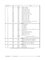
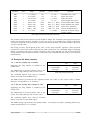
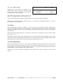
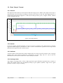
A complete table of the command codes is shown in Table 3.
7 . 2 . 1 Writing to the APV6
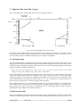
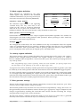
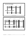
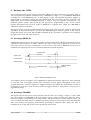
Data is written to the APV6 with one I2C transfer with two 8 bit data packets.
The first packet defines the APV address, t h e
second specifies a command register (in both cases
the read bit must be low) and the third specifies the
new value for the register.
Function or Variable
Command
Register Code
An example of an IPRE write operation is shown in
Figure 3
Error register
Mode register
00 00 00 1X
7 . 2 . 2 Reading from the APV6
Latency register
00 00 01 0X
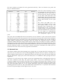
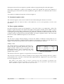
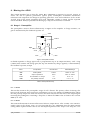
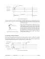
To read data from the APV6 the command register
must first be written. Reading requires two separate
I2C transfers.
00 00 00 01
IPRE
01 00 00 0X
ISHA
01 00 00 1X
IPSP
01 00 01 0X
ISFB
01 00 01 1X
VPRE
01 00 10 0X
The first packet defines the APV address (read bit
low), the second specifies the command register
(read bit high). Any further data packets are
ignored.
VSHA
01 00 10 1X
VADJ
01 00 11 0X
VCAS
01 00 11 1X
CLVL
01 01 00 0X
Transfer 2
Read the data back
CSKW
01 01 00 1X
Once the command register has been programmed
the APV6 may be read by a standard I2C read
sequence, the APV will respond with a single 8-bit
packet corresponding to the addressed data.
CDRV
01 01 01 0X
Transfer 1
apv6_manual.doc
Write the command register
Version: Draft
11
Table 3: Command Register Codes
16/10/96