1
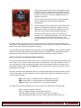
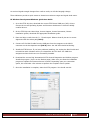
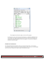
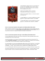
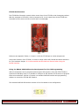
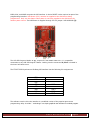
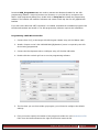
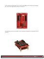
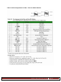
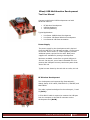
XBee® USB Multifunction Development Tool User Manual Compact multifunction USB development tool with advanced features: RF Wireless Development USB Development AVR Programming Typical Applications: Low-Power USB Wireless Development Low-Power CPU Based Wireless Development Low-Powered USB Instrumentation Power Supply The power supply for the development tool is derived from the USB port. The USB port provides +5 VDC power to the tool. An on-board +3.3 VDC regulator provides additional power required for the radio. Both power supplies are available for prototype development. Maximum available current from a typical USB port is 500 mA. On the tool, an on-board resettable PTC fuse protects the USB port from any continuous power drain above 500 mA. Typical current drawn by the tool with no radio; 400 uA. RF Wireless Development The development tool supports Digi International’s XBee® family of RF radios; DIGI 802.15.4, ZIG BEE, and DIGI-MESH. The radio is placed and aligned in the socket pair; J1 and J2 (Ref.A). A 5-Pin Mini-B cable is required to connect the USB port from the computer to the Mini-B connector on the development tool (Ref.B). ©RnD Warehouse 2010 Page 1 Radio communication and control is supported through the USB port. An on-board single chip; FTDI FT232R, provides a USB to asynchronous serial data and control interface to the radio. The entire USB bus protocol is handled on the chip. FTDI’s royalty-free Virtual Com Port (VCP) and D2XX drivers eliminate the requirement for USB driver development. Virtual COM port (VCP) drivers cause the USB device to appear as an additional COM port available to the PC. Application software can access the USB device in the same way as it would access a standard COM port. D2XX drivers allow direct access to the USB device through a DLL. Application software can access the USB device through a series of DLL function calls. The functions available are listed in the D2XX Programmer's Guide. The radio interface requires one cmos-level asynchronous serial port and two hardware flow control bits. The additional two flow control bits are used to provide the maximum RF Data rates between the radio and the USB interface, 250 kbs. Two LED USB bus traffic indicators are provided; TXD and RXD (Ref. C). The indicators indicate the communication status between the USB port and the FT232R. These indicators should be blinking when communication is established between the USB port and the FT232R. Radio Connection and Signal Strength Indicators The LED associated status indicator (ASC, Green), indicates the radio’s status of association with other radio’s on the network. When the radio is first powered-on, this LED will blink on-off at a very low frequency, once connected to another radio, this indicator will stay on as long as the association between radios remains (Ref. D). If the association is nulled, the LED will return to the blinking on-off state. The radio interface has an additional feature; three LED radio signal strength indicators (Ref. E). The LED radio signal strength indicators are three LED’s which provide an indication of the RF received signal strength. HSS (Green LED), is an abbreviation for High-Signal-Strength. MSS (Yellow LED), is an abbreviation for Mid-Signal-Strength. LSS (Red LED), is an abbreviation for Low-Signal-Strength. An output from the radio (RSSI, pin 6), is converted to this visual three-level bargraph. With With With With no signal, all LED’s will be off. Low-Signal-Strength, the Red LED will be on. Mid-Signal-Strength, the Red and Yellow LED’s will be on. High-Signal-Strength, the Red, Yellow, and Green LED’s will be on. ©RnD Warehouse 2010 Page 2 As received signal strength changes from radio to radio, so will this bargragh change. These indicators provide a quick means to determine maximum ranges and signal dead-zones. RF Wireless Development Windows Quick Start Guide 1. Go to the FTDI chip site, download the current FTDI Virtual COM port (VCP) drivers. Choose the correct Operating System and Processor Architecture. Select the WHQL certified drivers. 2. On the FTDI chip site Home Page, choose Support, choose Documents, Choose installation guides, download the appropriate installation guide. 3. Place and align a radio into the J1 - J2 socket pair. Observe that all pins are in correct alignment with the socket pair (Ref.A). 4. Connect a 5-Pin Mini-B cable from the USB port from the computer to the Mini-B connector on the development tool (Ref.B). Note: the ASC LED should be blinking. 5. Install the FTDI drivers. If you have problems installing, just unplug the Mini-B cable and reinstall the cable. Windows will try to reinstall the drivers. Note: the COM Port assignment when the drivers are successfully installed. 6. Download the current Digi International XCTU General Diagnostics and Utilities program. Install the program. (Link is on the Product page). Make sure you allow the installation program to update the Firmware Source Versions. Depending upon your connection speed, this could take a few minutes to perform the complete source update. 7. Once the installation is complete, start the XCTU program. You should see this: ©RnD Warehouse 2010 Page 3 Note: the USB Serial Port (COM4 in this case) should match the COM Port installed by the FTDI driver installation. 8. Leave the settings as is. The default Baud-Rate of the radio is 9600, Flow Control: None, Data Bits: 8, Parity: None, and Stop Bits: 1. Press Test/Query. You should see this: If you receive an error message: unable to communicate with the Modem, Press Retry and communication should be established. Note: the Modem type should match the Xbee model installed and note the firmware version. Basic communication is now established. Press OK to return to the Main Menu. 9. Next, we are going to check to see if there exists a new update for the firmware and update the firmware if a new version does exist. On the Main Menu, press the Modem Configuration Tab. The program moves the Remote Configuration Window: ©RnD Warehouse 2010 Page 4 Under Modem Parameters and Firmware; Press the Read button. The program scans the attached radio and reports the firmware command parameters. ©RnD Warehouse 2010 Page 5 The Modem, Function Set, Version (Firmware), and command parameters have all been filled in by the scan. 10. Press the Down-Arrow button on the Version. As you can see in our case, the current firmware version is highlighted and a new firmware version does exist. Select the new firmware; 10E8 and the command parameters are updated in the Window. 11. Under Modem Parameters and Firmware; Press the Write button. The program initializes the Modem and programs the new firmware into the Modem. Observe the USB indicators: TXD and RXD. They should be blinking as the program writes and reads to and from the Modem. 12. When the programming completes, Under Modem Parameters and Firmware; Press the Read button. The parameter window blanks as the program reads, at the end of the scan, the new firmware parameters 10E8 are updated. Note the new firmware version listing at the bottom of the window. ©RnD Warehouse 2010 Page 6 This completes the firmware update, close the XCTU program. It is beyond the scope of this manual to demonstrate any additional capabilities of the XCTU program. We suggest downloading the XCTU Users Guide for this program and exploring the additional capabilities of the XCTU program. The Link for this manual is located on the product page. RF Radio Port Bus Extension The XBee®/XBee-PRO Radio Modules contain an on-board microprocessor. This on-board microprocessor supports external inputs of Analog Voltages for ADC conversion, external Digital inputs and can be configured for Digital outputs including PWM outputs. ©RnD Warehouse 2010 Page 7 These additional support features are extended from the pins of the radio (A) to the P1 and P3 sockets (F). This port extension allows the user to harness the full capability of the radio. Reference the Appendix Table 1-02 for the XBee®/XBee-PRO module pin assignments. Reference the Appendix Table 1-01 for the P1 and P3 pin assignments. To enable PWM0, P1-6, remove the RSSI 2-pin jumper (G). Note: Signal Strength Indicators are disabled. To enable AD5 /DIO5, remove the ASCE 2-pin jumper (G). Note: Associated Status Indicator is disabled. How to control Data Acquisition through the local XBee®/XBee-PRO module XBee® modules connected to a host computer via the USB interface can be controlled using the AT commands described in the XBee®/XBee-PRO OEM RF Module product manual. Refer to this product manual for a complete description of the XBee AT command set. How to control Data Acquisition through a remote XBee®/XBee-PRO module A remote XBee®/XBee-PRO module must first be configured for Data Acquisition before actual commands can be sent to acquire data. Using API commands, we can send AT mode commands to read and write remote data. This tutorial (Xbee API Commands), provides a detailed explanation on configuring and controlling a remote radio. The link to this tutorial is located on the product page. It is also possible to use the remote XBee®/XBee-PRO module as a RF serial port. You could add serial D/A’s, A/D’s, and any devices that have a serial port providing the logic-levels are radio compatible; +3.3 VDC . Device selection can be controlled by the XBee® Digital outputs. For remote XBee®/XBee-PRO Data Acquisition development, an optional AC/DC power supply can be purchased to supply power to the remote unit as opposed to USB power. The power supply has a Mini‐ B type termination. Current is limited to the USB PTC fuse value ‐ 500mA. Part Number: 22‐001 ©RnD Warehouse 2010 Page 8 Using the XBee® USB Multifunction Development Tool for FTDI Development The FTDI FT232R is a USB to serial UART interface with optional clock generator output, and the new FTDIChip-ID™ security dongle feature. In addition, asynchronous and synchronous bit bang interface modes are available. The FT232R fully integrates an EEPROM, Oscillator and USB interface into the device. The FTDI 232R operates from the factory in the Normal‐Mode. In the Normal-Mode of operation, bytes sent to the FT232R through the USB interface are transmitted out serially through the TXD pin. Bytes received serially on the RXD pin are transmitted back through the USB interface. This device performs asynchronous 7 or 8 bit parallel to serial and serial to parallel conversion of the data on this interface. The Baud Rate for the serial interface is determined by an internal Baud Rate Generator. Control signals supported in this mode include RTS, CTS, DSR, DTR, DCD and RI. The UART Controller also provides a transmitter enable control signal pin option (TXDEN#) to assist with interfacing to RS485 devices. Additional features in this mode; TXLED# - for pulsing an LED upon USB transmission of data, RXLED# - for pulsing an LED upon receiving USB data, PWREN# - Power control for high power, bus powered designs and SLEEP# - indicates that the device going into USB suspend mode. NORMAL‐MODE CONTROL LINES TXD RXD RTS CTS DTR DSR DCD RI CBUS I/O CONFIGURATION: NORMAL‐MODE CONTROL LINES TXLED# RXLED# TXDEN# PWREN# SLEEP# ©RnD Warehouse 2010 Page 9 In the Normal-Mode, we basically have a UART with programmable Baud Rates and Flow Control. In Windows, the device would appear as a legacy COM port using the FTDI VCP drivers. Bit Bang Mode The Bit Bang Mode allows the user to configure the device into different configurations other than the Normal-Mode. There are three types of Bit Bang modes for the FT232R; Asynchronous, Synchronous and CBUS. The different Bit Bang modes are set by the the D2XX command: FT_SetBitMode. The values for the different modes are shown below: Asynchronous FT_SetBitMode = 1 Synchronous FT_SetBitMode = 4 CBUS FT_SetBitMode = 20 Resetting the FT_SetBitMode= 0, Resets the Device back to Normal‐Mode. The FTDI D2XXX drivers must be used to access the Bit Bang Mode features. These drivers are provided as separate DLL files and are simple to interface to. You must remove VCP drivers before you install the D2XXX drivers. Asynchronous Bit Bang Mode , This mode is simply an 8 bit Parallel port where each pin can be set as an input or an output with each pin being independent of each other. The rate that the data is written to or read from the port is controlled by the Baud rate generator. The Normal-Mode Control lines become: TXD RXD RTS CTS DTR DSR DCD RI D0 <‐> D1<‐> D2<‐> D3<‐> D4<‐> D5<‐> D6<‐> D7<‐> ©RnD Warehouse 2010 Page 10 It is possible in this mode to extend the internal Read (RD) Write (WR) strobes to the CBUS pins in order to externally latch written data or strobe to read data. These extended signals can be assigned to any one of the CBUS0 – CBUS3 pins. Synchronous Bit Bang Mode In this mode, data is only read from the device when the device is being written to. It is a “read-modify-write” cycle. Data is Read from the port, possibly modified, and then rewritten to the port. The Data Port assignment (D0-D7) in this mode, is the same as the Asynchronous pin assignment. All data transfer is controlled by the synchronous Read (RD) Write (WR) strobes from the CBUS pins. These signals can be assigned to any one of the CBUS0 – CBUS3 pins. Asynchronous and Synchronous Bit Bang types are commonly used to transfer large buffers of data with FT_Write and FT_Read. CBUS Bit Bang Mode This mode is simply a 4 bit Parallel port (CBUS0-CBUS3), where each pin can be set as an input or an output with each pin being independent of each other. The CBUS Bit Bang mode must be configured in the FT232R EEPROM. The CBUS must be set to an I/O configuration. Do not forget to re‐enumerate the device after programming or it will not work. The CBUS Bit Bang is much slower in operation than the Asynchronous or Synchronous Bit Bang; it is byte oriented. It is important to note; that the CBUS is a unique port initiated by a separate mode. It is not implied that this port can be used in conjunction with Asynchronous or Synchronous Bit Bang to obtain a 12 bit port. It will not work. For more detailed information about these modes see: FTDI Application Note AN_232R-01 for the FT232R and FT245R Bit Bang Modes. ©RnD Warehouse 2010 Page 11 FT232R Bus Extension The FT232R Bus Extension extends all the control lines of the FT232R to the Prototyping sockets. With the exception of CTS#/D3, which is located on P3-16, all control lines of the FT232R are extended from the device to the to the P2 and P4 sockets (H). Reference the Appendix Tables; 1-03 and 1-04 for the FT232R pin-to-socket assignments. Using these features of the FT232R, it is east to design USB to SPI, Parallel and Serial interfaces for your hardware designs. It is recommended that the Radio be removed when using the Parallel interface. Using the XBee® USB Multifunction Development Tool for AVR Programming AVR microcontrollers can be programmed through an SPI interface. Using the FTDI FT232R in Synchronous Bit Bang mode, it is possible to configure an SPI interface on the device to program these microcontrollers. All that is required is a standard AVR ISP interface and programming software to control the FT232R SPI interface. The standard AVR ISP SPI interface consists of a 6-Pin Header in this configuration: ©RnD Warehouse 2010 Page 12 MISO, SCK, and MOSI comprise the SPI interface. A device RESET is also required as part of the programming interface. USB Power (VCC) can also be supplied to the AVR device being programmed. Only use this feature when power is not being supplied to the AVR device by another power source. The USB Power is supplied through a 2-Pin jumper: USB AVR PWR (J). The AVR ISP Program Header J4 (I), requires a 6-Pin Ribbon cable for a 1-1 compatible connection to any AVR ISP Program Header. Looking into the connector J4, Pin 1 is located in the lower left-hand corner. The FTDI FT232R Synchronous Bit Bang SPI interface Has the following Pin assignments: TXD RXD RTS CTS DTR DSR DCD RI MISO‐> SCK‐> MOSI<‐ RESET‐> The software used to drive the interface is a modified version of the popular open-source programming utility ‘avrdude’. ‘avrdude-gui’ is a simple graphical user interface for avrdude program. ©RnD Warehouse 2010 Page 13 Download AVR_Programmer.rar, this archive contains the Windows Installer for the AVR programming software. Unzip this archive to a Directory on your Disk Drive, navigate to the folder: \AVR Programmer\Setup Files, double-click on setup.msi and install the programming software. The Installer will install the software and create a Desk-top Icon for the graphical user interface. If you don’t have Microsoft .NET framework 2.0 installed, download the installation program from the Microsoft website and install it. The AVR programming software requires this installation. Programming a AVR Microcontroller 1. Connect from J4 (I) to the target AVR ISP Program Header using a 6-Pin Ribbon cable. 2. Install a Jumper on the 2-Pin USB AVR PWR (J) Header if power is required by the AVR device being programmed. 3. Connect the Development tool to a USB port using a 5-Pin Mini USB cable. 4. Double-click the avrdude-gui Icon to run the programming software. 5. The first time you run the avrdude-gui program, you will need to configure the default settings. 6. First you need to specify the location of the program avrdude.exe in the avrdude.exe File field. Press the browse button at the right of the field to locate the file. ©RnD Warehouse 2010 Page 14 Typical location for this file is illustrated for a ‘C:\Program Files\’ installation. 7. Press the pull-down button next to the ‘Programmer’ field and select ‘FT232 Synchronous BitBang (diecimila)’. 8. Press the pull-down button next to the ‘Device’ field and select your microcontroller, in this case ‘ATmega1280 (m1280)’. 9. In the ‘Command line Option’ field, enter ‘-P ft0 –B 4800’. "-P ft0" is the FT232R BitbangPort settings. "-B 4800" sets the slow clock mode setting. 10. Test the connection by reading the fuse-bits. Press the ‘Read’ button in the ‘Fuse’ area. If you get an error, check your wiring and try again. ©RnD Warehouse 2010 Page 15 If the fuse-bits can be read, then you’re ready to proceed to programming your device. 11. Press the browse button next to the ‘Flash’ field and navigate to and select the hex file you want to use. Press the ‘Erase – Write – Verify’ button to program the part. 12. Programming completed! Remove the ISP programming cable. Additional Programmer functions include: Chip Erase - This will reset the contents of the flash ROM and EEPROM to the value ‘0xff’, and clear all lock bits. Terminal – MS DOS Command Prompt Window Port – Specifies the Port the Programmer is connected to. This is not used in our case. Display Window – Response Display Window from the core avrdude program. Fuse Bits – You can write new values and read the status of the Fuse Bits. Appendix Table 1-05 provides a list of AVR microcontrollers supported by the Programmer. Using The XBee® Stackable Prototype Board for XBee®/XBee-PRO and FT232R Prototype Development Prototypes for XBee®/XBee-PRO Data Acquisition and FT232R applications can be assembled quickly using the XBee® Stackable Prototype board. The stackable prototype board provides a 1-for-1 signal extension from both the RF Radio Port and the FT232R Bus. ©RnD Warehouse 2010 Page 16 On the stackable prototype board, the P1 and P3 sockets (K) provide a RF Radio Port Extension and , the P2 and P4 (L) sockets provide the FT232R Bus. The prototype board can accommodate various prototyping configurations for application specific hardware. ©RnD Warehouse 2010 Page 17 Appendix Table 1-01 Pin Assignments for the XBee USB Multifunctional P1 and P3 Sockets: P1 SKT & Pin# Name Direction P1-1 VCC - Power Supply +5 VDC P1-2 DOUT Output XBEE UART Data Out P1-3 DIN Input P1-4 DO8 Output XBEE Digital Output 8 P1-5 VCC1 - Power Supply +3.3 VDC P1-6 PWM0/RSSI Output P1-7 PWM1 Output P1-8 SGND - P1-9 P1-10 P3 SKT & Pin# P3-11 Remote /DTR Connected To: XBEE UART Data In XBEE PWM 0/RX Signal Strength Indicator XBEE PWM1 Signal Ground Input Remote /DTR Flow Control GND - Ground Name Direction Connected To: AD4/DIO4 Either XBEE Analog Input 4 or Digital I/O 4 Remote /RTS Flow Control P3-12 Remote /RTS Input P3-13 ON /SLEEP Output P3-14 VREF Input P3-15 Associate / AD5 / DIO5 Either XBEE ASC Indicator/Analog In 5/Dig I/O 5 P3-16 /CTS / DIO7/D3 Either XBEE CTS/Digital I/O7- FTDI CTS#/D3 XBEE Module Status Indicator +3.3 VDC Reference for XBEE A/D P3-17 AD3 / DIO3 Either XBEE Analog In 3 or Digital I/O 3 P3-18 AD2 / DIO2 Either XBEE Analog In 2 or Digital I/O 2 P3-19 AD1 / DIO1 Either XBEE Analog In 1 or Digital I/O 1 P3-20 AD0 / DIO0 Either XBEE Analog In 0 or Digital I/O 0 NOT DIRECTLY CONNECTED TO THE XBEE RADIO Appendix ©RnD Warehouse 2010 Page 18 Table 1-02 Pin Assignments for XBee – Xbee Pro Radio Modules ©RnD Warehouse 2010 Page 19 Appendix Table 1-03 Pin Assignments for the XBee USB Multifunctional FTDI P2 and P4 Sockets: P2 SKT & Pin# Name Direction P2-1 VCC - P2-2 RXD/D1 Input/Either FTDI RXD/D1 P2-3 TXD/D0 Output/Either FTDI TXD/D0 P2-4 NC None No Connection P2-5 VCC1 - P2-6 NC None No Connection P2-7 NC None No Connection P2-8 SGND - Signal Ground DTR#/D4 Either FTDI DTR#/D4 GND - Ground P2-9 P2-10 P4 SKT & Pin# Connected To: Power Supply +5 VDC Power Supply +3.3 VDC Name Direction Connected To: P4-11 RTS#/D2 Either FTDI RTS#/D2 P4-12 DSR#/D5 Either FTDI DSR#/D5 P4-13 CBUS1 Output P4-14 VREF Input P4-15 CBUS0 Output P4-16 DCD#/D6 FTDI CBUS1 +3.3 VDC Voltage Reference Either FTDI CBUS0 FTDI DCD#/D6 P4-17 CBUS3 Output FTDI CBUS3 P4-18 CBUS2 Output FTDI CBUS2 P4-19 CBUS4 Output FTDI CBUS4 P4-20 RI#/D7 Either FTDI RI#/D7 Note: FTDI CTS#/D3 is located on P3-16 ©RnD Warehouse 2010 Page 20 Appendix Table 1-04 Simplified Pin Assignments for the FTDI FT232R Breakout: FTDI Pin Name D0 P2-3 D1 P2-2 D2 P4-11 D3 P3-16 D4 P2-9 D5 P4-12 D6 P4-16 D7 P4-20 FTDI Pin Name Connected To: CBUS0 P4-15 CBUS1 P4-13 CBUS2 P4-18 CBUS3 P4-17 FTDI Pin Name Connected To: Connected To: TXD P2-3 RXD P2-2 RTS P4-11 CTS P3-16 DTR P2-9 DSR P4-12 DCD P4-16 RI P4-20 ©RnD Warehouse 2010 Page 21 Appendix Table 1-05 List of supported AVR Microcontrollers by the Programmer : AT90CAN128 AT90PWM2 AT90PWM2B AT90PWM3 AT90PWM3B AT90s1200 AT90s2313 AT90s2333 AT90s2343 (also AT90s2323 and ATtiny22) AT90s4414 AT90s4433 AT90s4434 AT90s8515 AT90s8535 AT90USB1286 AT90USB1287 AT90USB646 AT90USB647 ATmega103 ATmega128 ATmega128RFA1 ATmega1280 ATmega1281 ATmega1284P ATmega16 ATmega161 ATmega162 ATmega163 ATmega164 ATmega164P ATmega168 ATmega168P ATmega169 ATmega2560 ATmega2561 ATmega32 ATmega324 ATmega324P ATmega325 ATmega3250 ATmega328P ATmega329 ATmega329P ATmega3290 ATmega3290P ATmega48 ATmega64 ATmega640 ATmega644 ATmega644P ATmega645 ATmega6450 ATmega649 ATmega6490 ATmega8 ATmega8515 ATmega8535 ATmega88 ATmega88P ATtiny11 ATtiny12 ATtiny13 ATtiny15 ATtiny24 ATtiny25 ATtiny26 ATtiny261 ATtiny44 ATtiny45 ATtiny461 ATtiny84 ATtiny85 ATtiny861 ATtiny88 ATtiny2313 ©RnD Warehouse 2010 Page 22