1
DIGITAL Alpha VME 5/352 and
5/480 Single-Board Computers
Technical Reference
Order Number: EK–VME54–TM. A01
This manual discusses DIGITAL Alpha VME 5/352 and 5/480 single-board computer (SBC) address mapping, VME interface, system interrupts, and system registers.
Revision/Update Information:
Digital Equipment Corporation
Maynard, Massachusetts
This is a new manual.
First Printing, February 1998
The information in this document is subject to change without notice and should not be construed as a commitment by
Digital Equipment Corporation.
Digital Equipment Corporation assumes not responsibility for any errors that might appear in this document.
The software described in this document is furnished under license and may be used or copied only in accordance with the
terms of such license. No responsibility is assumed for the use or reliability of software or equipment that is not supplied
by Digital Equipment Corporation or its affiliated companies.
Restricted Rights: Use, duplication, or disclosure by the U.S. Government is subject to restrictions as set forth in
subparagraph (c) (1) (ii) of the Rights in Technical Data and Computer Software clause at DFARS 252.227–7013.
FCC Notice:
This equipment has been tested and found to comply with the limits for a Class A digital device, pursuant to Part 15 of the
FCC Rules. These limits are designed to provide reasonable protection against harmful interference when the equipment is
operated in a commercial environment. This equipment generates, uses, and can radiate radio frequency energy and, if not
installed and used in accordance with the instruction manual, may cause harmful interference to radio communications.
Operation of this equipment in a residential area is likely to cause harmful interference, in which case the user will be
required to correct the interference at his own expense.
Warning!
This is a Class A product. In a domestic environment this product may cause radio interference in which case the user may
be required to take adequate measures.
Achtung!
Dieses ist ein Gerät der Funkstörgrenzwertklasse A. In Wohnbereichen können bei Betrieb dieses Gerätes
Rundfunkstörungenauftreten, in welchen Fällen der Benutzer für entsprechende Gegenmaßnahmen verantwortlich ist.
Attention!
Ceci est un produit de Classe A. Dans un environment domestique, ce produit risque de créer des interférences
radioélectriques, il appartiendra alors à l'utilisateur de prendre les mesures spécifiques appropriées.
Canadian EMC Notice:
“This Class [A] digital apparatus meets all requirements of the Canadian Interference-Causing Equipment Regulations.”
“Cet appareil numerique de la class [A] respecte toutes les exigences du Reglement sur le materiel broilleur du Canada.”
© Digital Equipment Corporation 1998. All rights reserved.
Printed in U.S.A.
The following are trademarks of Digital Equipment Corporation: DECchip, DECnet, DECpc, DIGITAL, OpenVMS,
ThinWire, VAX, and the DIGITAL logo.
The following are third-party trademarks:
DALLAS is a registered trademark of Dallas Systems Corporation.
DIGITAL UNIX and UNIX are registered trademarks licensed exclusively by X/Open Company Ltd.
IBM is a registered trademark of International Business Machines Corporation.
Intel is a trademark of Intel Corporation.
VIC64 is a trademark of Cypress Semiconductor Corporation.
VxWorks is a registered trademark of Wind River Systems, Inc.
All other trademarks and registered trademarks are the property of their respective holders.
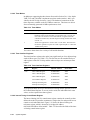
Contents
1
Introduction
1.1 Functional Component Overview. . . . . . . . . . . . . . . . . . . . . . . . . . . . . . . . . . . . . . . . .
1.2 21164 Alpha Microprocessor . . . . . . . . . . . . . . . . . . . . . . . . . . . . . . . . . . . . . . . . . . . .
1.3 21172 Core Logic Chipset . . . . . . . . . . . . . . . . . . . . . . . . . . . . . . . . . . . . . . . . . . . . . .
1.3.1 Chipset Components . . . . . . . . . . . . . . . . . . . . . . . . . . . . . . . . . . . . . . . . . . . . . . .
1.3.2 Chipset Features . . . . . . . . . . . . . . . . . . . . . . . . . . . . . . . . . . . . . . . . . . . . . . . . . .
1.4 Bcache Subsystem . . . . . . . . . . . . . . . . . . . . . . . . . . . . . . . . . . . . . . . . . . . . . . . . . . . .
1.5 Memory Subsystem . . . . . . . . . . . . . . . . . . . . . . . . . . . . . . . . . . . . . . . . . . . . . . . . . . .
1.6 SROM . . . . . . . . . . . . . . . . . . . . . . . . . . . . . . . . . . . . . . . . . . . . . . . . . . . . . . . . . . . . . .
1.7 Clock Interface . . . . . . . . . . . . . . . . . . . . . . . . . . . . . . . . . . . . . . . . . . . . . . . . . . . . . . .
1.8 PCI Interface. . . . . . . . . . . . . . . . . . . . . . . . . . . . . . . . . . . . . . . . . . . . . . . . . . . . . . . . .
1.8.1 Ethernet Controller . . . . . . . . . . . . . . . . . . . . . . . . . . . . . . . . . . . . . . . . . . . . . . . .
1.8.2 SCSI Controller . . . . . . . . . . . . . . . . . . . . . . . . . . . . . . . . . . . . . . . . . . . . . . . . . . .
1.8.3 PMC I/O Companion Card . . . . . . . . . . . . . . . . . . . . . . . . . . . . . . . . . . . . . . . . . .
1.9 Nbus Interface. . . . . . . . . . . . . . . . . . . . . . . . . . . . . . . . . . . . . . . . . . . . . . . . . . . . . . . .
1.9.1 Interrupt Controllers . . . . . . . . . . . . . . . . . . . . . . . . . . . . . . . . . . . . . . . . . . . . . . .
1.9.2 Flash ROM . . . . . . . . . . . . . . . . . . . . . . . . . . . . . . . . . . . . . . . . . . . . . . . . . . . . . .
1.9.3 TOY Clock . . . . . . . . . . . . . . . . . . . . . . . . . . . . . . . . . . . . . . . . . . . . . . . . . . . . . .
1.9.4 Watchdog Timer . . . . . . . . . . . . . . . . . . . . . . . . . . . . . . . . . . . . . . . . . . . . . . . . . .
1.9.5 NVRAM . . . . . . . . . . . . . . . . . . . . . . . . . . . . . . . . . . . . . . . . . . . . . . . . . . . . . . . .
1.9.6 Interval Timer . . . . . . . . . . . . . . . . . . . . . . . . . . . . . . . . . . . . . . . . . . . . . . . . . . . .
1.9.7 Keyboard and Mouse Controller . . . . . . . . . . . . . . . . . . . . . . . . . . . . . . . . . . . . . .
1.9.8 Super I/O Chip. . . . . . . . . . . . . . . . . . . . . . . . . . . . . . . . . . . . . . . . . . . . . . . . . . . .
1.10 VME Interface . . . . . . . . . . . . . . . . . . . . . . . . . . . . . . . . . . . . . . . . . . . . . . . . . . . . . .
1.10.1 VIP Chip . . . . . . . . . . . . . . . . . . . . . . . . . . . . . . . . . . . . . . . . . . . . . . . . . . . . . . .
1.10.2 VIC64 and CY7C964 Chips . . . . . . . . . . . . . . . . . . . . . . . . . . . . . . . . . . . . . . . .
1.10.3 Address Mapping and the Scatter-Gather Map . . . . . . . . . . . . . . . . . . . . . . . . . .
2
1-1
1-3
1-4
1-4
1-5
1-5
1-6
1-7
1-7
1-7
1-7
1-8
1-8
1-9
1-9
1-10
1-10
1-11
1-11
1-11
1-12
1-12
1-12
1-13
1-13
1-14
System Address Mapping
2.1 Address Space Overview . . . . . . . . . . . . . . . . . . . . . . . . . . . . . . . . . . . . . . . . . . . . . . .
2.1.1 Cached and Noncacheable Regions. . . . . . . . . . . . . . . . . . . . . . . . . . . . . . . . . . . .
2.1.2 Supported Address Spaces. . . . . . . . . . . . . . . . . . . . . . . . . . . . . . . . . . . . . . . . . . .
2.1.3 21164 Address Space. . . . . . . . . . . . . . . . . . . . . . . . . . . . . . . . . . . . . . . . . . . . . . .
2.2 PCI Dense Memory Space . . . . . . . . . . . . . . . . . . . . . . . . . . . . . . . . . . . . . . . . . . . . . .
2.2.1 Characteristics . . . . . . . . . . . . . . . . . . . . . . . . . . . . . . . . . . . . . . . . . . . . . . . . . . . .
2.2.2 Advantages Over Sparse Space . . . . . . . . . . . . . . . . . . . . . . . . . . . . . . . . . . . . . . .
2.2.3 Address Generation . . . . . . . . . . . . . . . . . . . . . . . . . . . . . . . . . . . . . . . . . . . . . . . .
2.2.4 Flash ROM Address Mapping. . . . . . . . . . . . . . . . . . . . . . . . . . . . . . . . . . . . . . . .
2.2.5 VME Address Mapping. . . . . . . . . . . . . . . . . . . . . . . . . . . . . . . . . . . . . . . . . . . . .
2.2.6 Gaining Access to PCI Dense Memory Space . . . . . . . . . . . . . . . . . . . . . . . . . . .
2.3 PCI Sparse Memory Space . . . . . . . . . . . . . . . . . . . . . . . . . . . . . . . . . . . . . . . . . . . . . .
2-1
2-1
2-2
2-5
2-5
2-6
2-6
2-7
2-7
2-8
2-8
2-8
iii
2.3.1 Low-Order Address Bits. . . . . . . . . . . . . . . . . . . . . . . . . . . . . . . . . . . . . . . . . . . .
2.3.2 High-Order Address Bits . . . . . . . . . . . . . . . . . . . . . . . . . . . . . . . . . . . . . . . . . . .
2.3.3 VME Address Mapping . . . . . . . . . . . . . . . . . . . . . . . . . . . . . . . . . . . . . . . . . . . .
2.3.4 Gaining Access to PCI Sparse Memory Space. . . . . . . . . . . . . . . . . . . . . . . . . . .
2.4 PCI Sparse I/O Space. . . . . . . . . . . . . . . . . . . . . . . . . . . . . . . . . . . . . . . . . . . . . . . . . .
2.4.1 High-Order Address Bits . . . . . . . . . . . . . . . . . . . . . . . . . . . . . . . . . . . . . . . . . . .
2.4.2 Address Decoding. . . . . . . . . . . . . . . . . . . . . . . . . . . . . . . . . . . . . . . . . . . . . . . . .
2.4.3 Address Generation . . . . . . . . . . . . . . . . . . . . . . . . . . . . . . . . . . . . . . . . . . . . . . .
2.4.4 Gaining Access to PCI Sparse I/O Space . . . . . . . . . . . . . . . . . . . . . . . . . . . . . . .
2.5 PCI Configuration Space . . . . . . . . . . . . . . . . . . . . . . . . . . . . . . . . . . . . . . . . . . . . . . .
2.5.1 Device Type Selection . . . . . . . . . . . . . . . . . . . . . . . . . . . . . . . . . . . . . . . . . . . . .
2.5.2 Address Generation . . . . . . . . . . . . . . . . . . . . . . . . . . . . . . . . . . . . . . . . . . . . . . .
2.5.3 CIA Chip Hardware Registers . . . . . . . . . . . . . . . . . . . . . . . . . . . . . . . . . . . . . . .
2.5.4 Gaining Access to PCI Configuration Space . . . . . . . . . . . . . . . . . . . . . . . . . . . .
2.6 Byte/Word PCI Space . . . . . . . . . . . . . . . . . . . . . . . . . . . . . . . . . . . . . . . . . . . . . . . . .
3
VME Interface
3.1 Services Supported by the VME Interface. . . . . . . . . . . . . . . . . . . . . . . . . . . . . . . . . .
3.2 VMEbus Address Mapping . . . . . . . . . . . . . . . . . . . . . . . . . . . . . . . . . . . . . . . . . . . . .
3.2.1 Address Mapping Overview . . . . . . . . . . . . . . . . . . . . . . . . . . . . . . . . . . . . . . . . .
3.2.2 Outbound Scatter-Gather Mapping. . . . . . . . . . . . . . . . . . . . . . . . . . . . . . . . . . . .
3.2.3 Inbound Scatter-Gather Mapping . . . . . . . . . . . . . . . . . . . . . . . . . . . . . . . . . . . . .
3.3 VME Interface Initialization . . . . . . . . . . . . . . . . . . . . . . . . . . . . . . . . . . . . . . . . . . . .
3.3.1 Configuring the PCI Interface to the VMEbus . . . . . . . . . . . . . . . . . . . . . . . . . . .
3.3.2 Programming Scatter-Gather RAM . . . . . . . . . . . . . . . . . . . . . . . . . . . . . . . . . . .
3.3.3 Configuring the VIC64 Chip . . . . . . . . . . . . . . . . . . . . . . . . . . . . . . . . . . . . . . . .
3.4 Requesting Ownership of the VMEbus . . . . . . . . . . . . . . . . . . . . . . . . . . . . . . . . . . . .
3.5 VME Data Transfers . . . . . . . . . . . . . . . . . . . . . . . . . . . . . . . . . . . . . . . . . . . . . . . . . .
3.5.1 Single Mode Transfers . . . . . . . . . . . . . . . . . . . . . . . . . . . . . . . . . . . . . . . . . . . . .
3.5.2 Block Mode Transfers . . . . . . . . . . . . . . . . . . . . . . . . . . . . . . . . . . . . . . . . . . . . .
3.5.3 Setting Up for Block Mode Transfers. . . . . . . . . . . . . . . . . . . . . . . . . . . . . . . . . .
3.5.4 Setting Up for Block Mode DMA Transfers . . . . . . . . . . . . . . . . . . . . . . . . . . . .
3.5.5 VME Interprocessor Communication . . . . . . . . . . . . . . . . . . . . . . . . . . . . . . . . . .
3.6 System Controller Operation . . . . . . . . . . . . . . . . . . . . . . . . . . . . . . . . . . . . . . . . . . . .
3.6.1 Controlling VMEbus Arbitration . . . . . . . . . . . . . . . . . . . . . . . . . . . . . . . . . . . . .
3.6.2 Controlling the System Clock. . . . . . . . . . . . . . . . . . . . . . . . . . . . . . . . . . . . . . . .
3.6.3 Controlling Timeout Timers . . . . . . . . . . . . . . . . . . . . . . . . . . . . . . . . . . . . . . . . .
3.6.4 Handling VMEbus Interrupts . . . . . . . . . . . . . . . . . . . . . . . . . . . . . . . . . . . . . . . .
3.7 Byte Swapping . . . . . . . . . . . . . . . . . . . . . . . . . . . . . . . . . . . . . . . . . . . . . . . . . . . . . . .
3.7.1 DC7407 Byte Swapping . . . . . . . . . . . . . . . . . . . . . . . . . . . . . . . . . . . . . . . . . . . .
3.7.2 VIC64 Byte Swapping . . . . . . . . . . . . . . . . . . . . . . . . . . . . . . . . . . . . . . . . . . . . .
4
3-1
3-2
3-2
3-4
3-7
3-10
3-10
3-11
3-12
3-16
3-16
3-16
3-16
3-16
3-16
3-18
3-19
3-19
3-20
3-20
3-21
3-22
3-22
3-23
System Interrupts
4.1 Overview of System Interrupts . . . . . . . . . . . . . . . . . . . . . . . . . . . . . . . . . . . . . . . . . .
4.2 Interrupts Handled by the Xilinx Controller . . . . . . . . . . . . . . . . . . . . . . . . . . . . . . . .
4.3 Interrupts Handled by the VIC64 Chip . . . . . . . . . . . . . . . . . . . . . . . . . . . . . . . . . . . .
4.3.1 Local Device Interrupts . . . . . . . . . . . . . . . . . . . . . . . . . . . . . . . . . . . . . . . . . . . .
4.3.2 VMEbus Interrupts . . . . . . . . . . . . . . . . . . . . . . . . . . . . . . . . . . . . . . . . . . . . . . . .
4.3.3 Status/Error Interrupts . . . . . . . . . . . . . . . . . . . . . . . . . . . . . . . . . . . . . . . . . . . . .
4.4 Interrupts Handled by the SIO Chip . . . . . . . . . . . . . . . . . . . . . . . . . . . . . . . . . . . . . .
4.4.1 Nonmaskable System Events . . . . . . . . . . . . . . . . . . . . . . . . . . . . . . . . . . . . . . . .
4.4.2 CIA Interrupt . . . . . . . . . . . . . . . . . . . . . . . . . . . . . . . . . . . . . . . . . . . . . . . . . . . .
iv
2-9
2-9
2-9
2-9
2-10
2-10
2-10
2-10
2-10
2-11
2-11
2-12
2-12
2-12
2-13
4-1
4-3
4-4
4-5
4-5
4-5
4-6
4-6
4-7
4.5 Module Resets . . . . . . . . . . . . . . . . . . . . . . . . . . . . . . . . . . . . . . . . . . . . . . . . . . . . . . .
5
4-7
System Registers
5.1 Gaining Access to System Registers . . . . . . . . . . . . . . . . . . . . . . . . . . . . . . . . . . . . . .
5.2 Ethernet Controller Registers . . . . . . . . . . . . . . . . . . . . . . . . . . . . . . . . . . . . . . . . . . . .
5.2.1 Ethernet Controller PCI Configuration Registers . . . . . . . . . . . . . . . . . . . . . . . . .
5.2.2 Ethernet Controller Control/Status Registers . . . . . . . . . . . . . . . . . . . . . . . . . . . .
5.2.3 Ethernet ROM Control/Status Register . . . . . . . . . . . . . . . . . . . . . . . . . . . . . . . . .
5.3 SCSI Controller Registers. . . . . . . . . . . . . . . . . . . . . . . . . . . . . . . . . . . . . . . . . . . . . . .
5.3.1 SCSI Controller PCI Configuration Registers. . . . . . . . . . . . . . . . . . . . . . . . . . . .
5.3.2 SCSI Controller Control/Status Registers . . . . . . . . . . . . . . . . . . . . . . . . . . . . . . .
5.4 SIO Chip and Nbus Registers . . . . . . . . . . . . . . . . . . . . . . . . . . . . . . . . . . . . . . . . . . . .
5.4.1 SIO Chip PCI Configuration Space. . . . . . . . . . . . . . . . . . . . . . . . . . . . . . . . . . . .
5.4.2 SIO CHIP Nonmaskable Interrupt Control/Status Register . . . . . . . . . . . . . . . . .
5.4.3 Module Registers. . . . . . . . . . . . . . . . . . . . . . . . . . . . . . . . . . . . . . . . . . . . . . . . . .
5.4.4 Super I/O Chip Registers. . . . . . . . . . . . . . . . . . . . . . . . . . . . . . . . . . . . . . . . . . . .
5.4.5 TOY Clock, Watchdog Timer, and NVRAM Registers . . . . . . . . . . . . . . . . . . . .
5.4.6 Interval Timer Registers . . . . . . . . . . . . . . . . . . . . . . . . . . . . . . . . . . . . . . . . . . . .
5.4.7 Keyboard and Mouse Controller Registers . . . . . . . . . . . . . . . . . . . . . . . . . . . . . .
5.5 Summary of VME Interface Registers . . . . . . . . . . . . . . . . . . . . . . . . . . . . . . . . . . . . .
5-1
5-2
5-2
5-3
5-3
5-4
5-4
5-5
5-8
5-8
5-13
5-15
5-25
5-26
5-31
5-34
5-35
Figures
1–1
1–2
1–3
1–4
2–1
2–2
2–3
2–4
3–1
3–2
3–3
3–4
3–5
3–6
3–7
3–8
4–1
5–1
5–2
5–3
5–4
5–5
5–6
5–7
5–8
5–9
5–10
5–11
5–12
5–13
5–14
Alpha VME 5/352 and 5/480 Functional Components . . . . . . . . . . . . . . . . . .
21164 Alpha Microprocessor Functional Block Diagram. . . . . . . . . . . . . . . .
Level 3 Bcache Array . . . . . . . . . . . . . . . . . . . . . . . . . . . . . . . . . . . . . . . . . . .
PCI-to-VME Interface Components . . . . . . . . . . . . . . . . . . . . . . . . . . . . . . . .
21164 Microprocessor Address Space . . . . . . . . . . . . . . . . . . . . . . . . . . . . . .
21164 Address Space Configuration . . . . . . . . . . . . . . . . . . . . . . . . . . . . . . . .
Flash ROM Layout/Addressing. . . . . . . . . . . . . . . . . . . . . . . . . . . . . . . . . . . .
PCI Configuration Space Definition . . . . . . . . . . . . . . . . . . . . . . . . . . . . . . . .
Mapping of VME_WINDOW_1 and VME_WINDOW_2 . . . . . . . . . . . . . . .
Mapping Pages From PCI Address Space to VME Address Space . . . . . . . .
PCI-to-VMEbus Outbound Address Translation . . . . . . . . . . . . . . . . . . . . . .
Mapping Pages from VME Address Space to PCI Address Space . . . . . . . . .
VME Address Decoding . . . . . . . . . . . . . . . . . . . . . . . . . . . . . . . . . . . . . . . . .
VMEbus-to-PCI Inbound Address Translation for A32 . . . . . . . . . . . . . . . . .
Swap Modes . . . . . . . . . . . . . . . . . . . . . . . . . . . . . . . . . . . . . . . . . . . . . . . . . .
Big Endian VME Byte Lane Formats . . . . . . . . . . . . . . . . . . . . . . . . . . . . . . .
Block Diagram of the Interrupt Logic . . . . . . . . . . . . . . . . . . . . . . . . . . . . . . .
Ethernet Controller PCI Configuration Registers . . . . . . . . . . . . . . . . . . . . . .
Ethernet ROM Control/Status Register (CSR9) . . . . . . . . . . . . . . . . . . . . . . .
SCSI Controller PCI Configuration Registers. . . . . . . . . . . . . . . . . . . . . . . . .
SIO Configuration Block. . . . . . . . . . . . . . . . . . . . . . . . . . . . . . . . . . . . . . . . .
Nonmaskable Interrupt Control/Status Register . . . . . . . . . . . . . . . . . . . . . . .
Module Display Control Register . . . . . . . . . . . . . . . . . . . . . . . . . . . . . . . . . .
Display Character Set . . . . . . . . . . . . . . . . . . . . . . . . . . . . . . . . . . . . . . . . . . .
Module Configuration Register . . . . . . . . . . . . . . . . . . . . . . . . . . . . . . . . . . . .
Interrupt/Mask Register 1 . . . . . . . . . . . . . . . . . . . . . . . . . . . . . . . . . . . . . . . .
Interrupt/Mask Register 2 . . . . . . . . . . . . . . . . . . . . . . . . . . . . . . . . . . . . . . . .
Interrupt/Mask Register 3 . . . . . . . . . . . . . . . . . . . . . . . . . . . . . . . . . . . . . . . .
Interrupt/Mask Register 4 . . . . . . . . . . . . . . . . . . . . . . . . . . . . . . . . . . . . . . . .
Memory Configuration Registers 0-3 . . . . . . . . . . . . . . . . . . . . . . . . . . . . . . .
Memory Identification Register. . . . . . . . . . . . . . . . . . . . . . . . . . . . . . . . . . . .
1-2
1-4
1-6
1-13
2-1
2-3
2-7
2-12
3-3
3-3
3-4
3-7
3-8
3-8
3-23
3-24
4-2
5-2
5-4
5-5
5-9
5-13
5-16
5-16
5-17
5-18
5-18
5-18
5-18
5-19
5-20
v
5–15
5–16
5–17
5–18
5–19
5–20
5–21
5–22
5–23
5–24
5–25
Module Control Register 1 . . . . . . . . . . . . . . . . . . . . . . . . . . . . . . . . . . . . . . .
Bcache Configuration Register . . . . . . . . . . . . . . . . . . . . . . . . . . . . . . . . . . . .
Reset Reason Registers. . . . . . . . . . . . . . . . . . . . . . . . . . . . . . . . . . . . . . . . . .
TOY Clock Command Register . . . . . . . . . . . . . . . . . . . . . . . . . . . . . . . . . . .
Watchdog Timer Field in the Module Control Register . . . . . . . . . . . . . . . . .
Watchdog Timer Fields in the TOY Clock Command Register. . . . . . . . . . .
Watchdog Timer Registers . . . . . . . . . . . . . . . . . . . . . . . . . . . . . . . . . . . . . . .
NVRAM Access . . . . . . . . . . . . . . . . . . . . . . . . . . . . . . . . . . . . . . . . . . . . . . .
82C54 Control/Status Register . . . . . . . . . . . . . . . . . . . . . . . . . . . . . . . . . . . .
82C54 Timer Data Access . . . . . . . . . . . . . . . . . . . . . . . . . . . . . . . . . . . . . . .
Timer Interrupt Status Register. . . . . . . . . . . . . . . . . . . . . . . . . . . . . . . . . . . .
5-21
5-23
5-24
5-27
5-29
5-29
5-29
5-30
5-33
5-34
5-34
21164 Physical Address Space Mappings . . . . . . . . . . . . . . . . . . . . . . . . . .
Services Offered by the VME Interface . . . . . . . . . . . . . . . . . . . . . . . . . . . . .
VME Address Windows . . . . . . . . . . . . . . . . . . . . . . . . . . . . . . . . . . . . . . . . .
PCI Address in an Outbound Scatter-Gather Map Entry . . . . . . . . . . . . . . . .
VME Address in an Outbound Scatter-Gather Map Entry . . . . . . . . . . . . . . .
Formation of Address Modifier Codes from Scatter-Gather Entry . . . . . . . .
VME Address in an Inbound Scatter-Gather Map Entry . . . . . . . . . . . . . . . .
PCI Address in an Inbound Scatter-Gather Map Entry . . . . . . . . . . . . . . . . .
VME PCI Base Registers . . . . . . . . . . . . . . . . . . . . . . . . . . . . . . . . . . . . . . . .
Swap Modes . . . . . . . . . . . . . . . . . . . . . . . . . . . . . . . . . . . . . . . . . . . . . . . . . .
PCI BE# to Local A1,0 and SIZ1,0 Translation for Swap Modes . . . . . . . . .
Local Bus A1,0 and SIZ1,0 to PCI BE# Translation . . . . . . . . . . . . . . . . . . .
CPU Interrupt Assignments . . . . . . . . . . . . . . . . . . . . . . . . . . . . . . . . . . . . .
Mapping of Interrupt/Mask Registers to Interrupt Request Lines . . . . . . . . .
VIC64 Chip Interrupt Ranking . . . . . . . . . . . . . . . . . . . . . . . . . . . . . . . . . . .
Ethernet Controller Control/Status Registers . . . . . . . . . . . . . . . . . . . . . . . . .
SCSI Controller Control/Status Registers . . . . . . . . . . . . . . . . . . . . . . . . . . .
SIO PCI-to-Nbus Bridge Operating Address Space . . . . . . . . . . . . . . . . . . .
PCI Control Register. . . . . . . . . . . . . . . . . . . . . . . . . . . . . . . . . . . . . . . . . . . .
Nonmaskable Interrupt Control/Status Register Bits . . . . . . . . . . . . . . . . . . .
Module Registers . . . . . . . . . . . . . . . . . . . . . . . . . . . . . . . . . . . . . . . . . . . . . .
Module Configuration Register . . . . . . . . . . . . . . . . . . . . . . . . . . . . . . . . . . .
Presence Detect Bits . . . . . . . . . . . . . . . . . . . . . . . . . . . . . . . . . . . . . . . . . . . .
Presence Detect Bits 4-1 . . . . . . . . . . . . . . . . . . . . . . . . . . . . . . . . . . . . . . . . .
Presence Detect Bit 5 . . . . . . . . . . . . . . . . . . . . . . . . . . . . . . . . . . . . . . . . . . .
Presence Detect 7-6 . . . . . . . . . . . . . . . . . . . . . . . . . . . . . . . . . . . . . . . . . . . .
Memory ID Bits . . . . . . . . . . . . . . . . . . . . . . . . . . . . . . . . . . . . . . . . . . . . . . .
Module Control Register 1 . . . . . . . . . . . . . . . . . . . . . . . . . . . . . . . . . . . . . .
Bcache Size and Speed Decode . . . . . . . . . . . . . . . . . . . . . . . . . . . . . . . . . . .
Reset Reason Registers. . . . . . . . . . . . . . . . . . . . . . . . . . . . . . . . . . . . . . . . . .
Super I/O Register Address Space Map . . . . . . . . . . . . . . . . . . . . . . . . . . . .
TOY Clock, Watchdog Timer, and NVRAM Address Space . . . . . . . . . . . .
TOY Clock Timekeeping Registers . . . . . . . . . . . . . . . . . . . . . . . . . . . . . . . .
TOY Clock Command Register . . . . . . . . . . . . . . . . . . . . . . . . . . . . . . . . . . .
Timers . . . . . . . . . . . . . . . . . . . . . . . . . . . . . . . . . . . . . . . . . . . . . . . . . . . . . . .
Timer Modes. . . . . . . . . . . . . . . . . . . . . . . . . . . . . . . . . . . . . . . . . . . . . . . . . .
Timer Interface Registers . . . . . . . . . . . . . . . . . . . . . . . . . . . . . . . . . . . . . . . .
Interval Timing Control/Status Register. . . . . . . . . . . . . . . . . . . . . . . . . . . . .
Keyboard and Mouse Controller Addresses . . . . . . . . . . . . . . . . . . . . . . . . . .
VME_IF_BASE + . . . . . . . . . . . . . . . . . . . . . . . . . . . . . . . . . . . . . . . . . . . . .
2-4
3-1
3-2
3-4
3-5
3-6
3-9
3-9
3-11
3-22
3-24
3-25
4-1
4-3
4-4
5-3
5-5
5-9
5-12
5-14
5-15
5-17
5-19
5-19
5-20
5-20
5-21
5-22
5-23
5-24
5-25
5-26
5-26
5-27
5-31
5-32
5-32
5-33
5-35
5-35
Tables
2–1
3–1
3–2
3–3
3–4
3–5
3–6
3–7
3–8
3–9
3–10
3–11
4–1
4–2
4–3
5–1
5–2
5–3
5–4
5–5
5–6
5–7
5–8
5–9
5–10
5–11
5–12
5–13
5–14
5–15
5–16
5–17
5–18
5–19
5–20
5–21
5–22
5–23
5–24
5–25
vi
Preface
Purpose of this Manual
This manual introduces the DIGITAL Alpha VME 5/352 and 5/480 single-board
computer (SBC) functional components and discusses technical details, including
address mapping, the VME interface, system interrupts, and system registers.
Intended Audience
This manual is for OEM system integrators who are designing and building a
DIGITAL Alpha VME 5/352 or 5/480 SBC into specific application systems.
These systems may range in scope from a single Alpha VME 5/352 or 5/480 SBC
to highly complex multiprocessor systems that include a variety of hardware.
This manual assumes that readers have prerequisite knowledge and experience
with the following:
•
System design
•
VMEbus design and specifications
•
System-level programming
Structure of this Manual
This manual consists of five chapters and an index organized as follows:
•
Chapter 1, Introduction, describes the functional components associated with
the DIGITAL Alpha VME 5/352 and 5/480 SBCs.
•
Chapter 2, Address Mapping, provides an address space overview and
describes the implementation PCI memory space.
•
Chapter 3, VME Interface, discusses the VME interface, including VME
address mapping, initialization, and usage.
•
Chapter 4, System Interrupts, provides an overview of system interrupts, identifies interrupts handled by the various controllers and chips, and module
resets.
•
Chapter 5, System Registers, describes system registers associated with the
Ethernet controller, interval timer, module, SCSI controller, SIO chip, timeof-year (TOY) clock, VME interface, and watchdog timer.
vii
Conventions
This section defines terminology, abbreviations, and other conventions used in
this manual.
Abbreviations
•
Register access
The following list describes the register bit and field abbreviations:
Bit/Field Abbreviation
Description
MBZ (must be zero)
Bits and fields specified as MBZ must be zero.
RO (read only)
Bits and fields specified as RO can be read but not written.
RW (read/write)
Bits and fields specified as RW can be read and written.
SBZ (should be zero)
Bits and fields specified as SBZ should be zero.
WO (write only)
Bits and fields specified as WO can be written but not
read
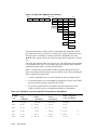
•
Binary multiples
The abbreviations K, M, and G (kilo, mega, and giga) represent binary multiples
and have the following values:
Abbreviation
Binary Multiple
K
210 (1024)
M
220 (1,048,576)
G
230 (1,073,741,824)
For example:
2 KB
= 2 kilobytes
= 2 x 210 bytes
4 MB
= 4 megabytes
= 4 x 220 bytes
8 GB
= 8 gigabytes
= 8 x 230 bytes
Addresses
Unless otherwise noted, addresses and offsets are hexadecimal values.
Bit Notation
Multiple-bit fields can include contiguous and noncontiguous bits contained in
angle brackets (< >). Multiple contiguous bits are indicated by a pair of numbers
separated by a colon ( : ). For example, <9:7,5,2:0> specifies bits 9, 8, 7, 5, 2, 1,
and 0. Similarly, single bits are frequently indicated with angle brackets. For
example, <27> specifies bit 27.
viii
Caution
Cautions indicate potential damage to equipment or loss of data.
Data Field Size
The term INTnn, where nn is one of 2, 4, 8, 16, 32, or 64, refers to a data field
of nn contiguous NATURALLY ALIGNED bytes. For example, INT4 refers to a
NATURALLY ALIGNED longword.
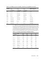
Data Units
The following data unit terminology is used throughout this manual.
Term
Words
Bytes
Bits
Other
Byte
1/2
1
8
−
Word
1
2
16
−
Longword
2
4
32
Longword
Quadword
4
8
64
2 Longwords
Octaword
8
16
128
2 Quadwords
Hexword
16
32
256
2 Octawords
Keyboard Keys
The following keyboard key conventions are used throughout this manual.
Convention
Example
Control key sequences are represented as Ctrl/ x.
Press Ctrl while you simultaneously press the x key
Ctrl/C
In plain text, key names match the name on the actual
key.
Return key
In tables, key names match the name of the actual key and appear in
square brackets ([ ]).
[Return]
Examples
Prompts, input, and output in examples are shown in a monospaced font. Interactive input is differentiated from prompts and system output with bold type. For
example:
>>> echo This is a test.[Return]
This is a test.
Ellipsis points indicate that a portion of an example is omitted.
ix
Names and Symbols
The following table lists typographical conventions used for names of various
items throughout this manual.
Items
Example
Bits
sysBus<32:2>
Commands
boot command
Command arguments
address argument
Command options
-sb option
Environment variables
AUTO_ACTION
Environment variable values
HALT
Files and pathnames
/usr/foo/bar
Pins
LIRQ pin
Register symbols
VIP_ICR register
Signals
iogrant signal
Variables
n, x, mydev
Note
Notes emphasize particularly important information.
Numbering
Numbers are decimal or hexadecimal unless otherwise indicated. The prefix 0x
indicates a hexadecimal number. For example, 19 is decimal, but 0x19 and 0x19A
are hexadecimal (see also Addresses). Otherwise, the base is indicated by a subscript; for example, 1002 is a binary number.
Ranges and Extents
Ranges are specified by a pair of numbers separated by two periods ( .. ) and are
inclusive. For example, a range of integers 0..4 includes the integers 0, 1, 2, 3,
and 4.
Extents are specified by a pair of numbers in angle brackets (< >) separated by a
colon ( : ) and are inclusive.
Bit fields are often specified as extents. For example, bits <7:3> specifies bits 7,
6, 5, 4, and 3.
Register and Memory Figures
Register figures have bit and field position numbering starting at the right (loworder) and increasing to the left (high-order).
Memory figures have addresses starting at the top and increasing toward the bottom.
x
Syntax
The following syntax elements are used throughout this manual. Do not type the
syntax elements when entering information.
Element
Example
Description
[]
[-file filename]
The enclosed items are optional.
|
-|+|=
Choose one of two or more items. Select
one of the items unless the items are
optional.
{}
{- | + | =}
You must specify one (and only one) of the
enclosed items.
()
(a,b,c)
You must specify the enclosed items
together.
...
arg...
You can repeat the preceding item one or
more times.
UNPREDICTABLE and UNDEFINED
This manual uses the terms UNPREDICTABLE and UNDEFINED. Their meanings are different and must be carefully distinguished.
UNPREDICTABLE results or occurrences do not disrupt the basic operation of
the processor. The processor continues to execute instructions in its normal manner. In contrast, UNDEFINED operations can halt the processor or cause it to lose
information.
For More Information
For more information, refer to the following:
•
Your supplier
•
The DIGITAL OEM web site at http://www.digital.com/oem.
•
The following DIGITAL Alpha VME 5/352 and 5/480 SBC documentation,
which is available on the DIGITAL OEM web site:
Document
Order Number
DIGITAL Alpha VME 5/352
and 5/480 Board Computer
Family Data Sheet
Description
Describes the DIGITAL Alpha 5/352 and 5/480
SBCs, highlighting product features and specifications.
DIGITAL Alpha VME 5/352 and
5/480 Single Board Computers
Cover Letter
EK–VME54–CL
Highlights important product information and
explains how to acquire the DIGITAL Alpha VME 5/
352 and 5/480 Single Board Computers User Manual and DIGITAL Alpha VME 5/352 and 5/480 Single Board Computers Technical Reference.
DIGITAL Alpha VME 5/352 and
5/480 Single Board Computers
Warranty and Parts Information
EK–VME54–WI
Explains the warranty of your DIGITAL Alpha
VME 5/352 or 5/480 SBC and provides parts information for ordering.
xi
Document
Order Number
Description
DIGITAL Alpha VME 5/352 and
5/480 Single Board Computers
Installation Guide
EK–VME54–IG
Explains how to install your DIGITAL Alpha VME
5/352 or 5/480 SBC. Use this guide if you need to
adjust jumper settings or remove and reinstall field
replaceable units (FRUs).
DIGITAL Alpha VME 5/352 and
5/480 Single Board Computers
User Manual
EK–VME54–UM
Introduces the product by discussing product specifications and requirements and describing the module and functional components. This manual also
explains how to use the console firmware and discusses diagnostics and troubleshooting.
DIGITAL Alpha VME 5/352 and EK–VME54–TM
5/480 Single Board Computers
Technical Reference (this manual)
This manual discusses system address mapping, the
VME interface, system registers, and system interrupts.
•
The following DIGITAL documentation:
Document
Order Number
Alpha Architecture Handbook
EC–QD2KB–TE
Alpha Microprocessors SROM Mini-Debugger User’s
Guide
EC–QHUXB–TE
Answers to Common Questions about PALcode for
Alpha AXP Systems
EC–N0647–72
Digital Semiconductor Alpha 21164 Microprocessor
Product Brief
EC–QP97C–TE
Digital Semiconductor 21052 PCI–PCI Bridge Data
Sheet
EC–QHURB–TE
Digital Semiconductor 21164 Alpha Microprocessor
Data Sheet
EC–QP98B–TE
Digital Semiconductor 21172 Core Logic Chipset Prod- EC–QUQHA–TE
uct Brief
Digital Semiconductor 21164 Alpha Microprocessor
Hardware Reference Manual
EC–QP99B–TE
Digital Semiconductor 21172 Core Logic Chipset Tech- EC–QUQJA–TE
nical Reference Manual
xii
DIGITAL UNIX Guide to Real-time Programming
AA–PS33D–TE
DIGITAL UNIX: Writing PCI Bus Device Drivers
AA–Q7RQC–TE
DIGITAL UNIX: Writing VMEbus Device Drivers
AA–Q0R7G–TE
PALcode for Alpha Microprocessors System Design
Guide
EC–QFGLC–TE
•
The following specifications are available through the indicated vendor or
organization:
Document
Vendor or Organization
CY7C9640 Specification
Cypress Semiconductor Corp.
Intel 82378ZB PCI-ISA Bridge Chip
Specification
Intel Corp.
PCI Local Bus Specification Rev 2.1
PCI Special Interest Group
Super I/O FDC37C6656T Specification Standard Microsystems Corp.
Symbios 53C810 SCSI Controller Spec- Symbios
ification
TOY clock DS1386 Specification
Dallas Semiconductor
VIC64 Specification
Cypress Semiconductor Corp.
xiii
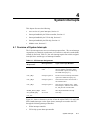
1
Introduction
This chapter introduces the functional components associated with the DIGITAL
Alpha VME 5/352 and 5/480 SBCs. The chapter begins with an overview (Section 1.1) and then briefly describes the following:
•
21164 Alpha microprocessor chip, Section 1.2
•
21172 core logic chipset, Section 1.3
•
Bcache subsystem, Section 1.4
•
Memory subsystem, Section 1.5
•
SROM, Section 1.6
•
Clock interface, Section 1.7
•
PCI interface, Section 1.8
•
Nbus interface, Section 1.9
•
VME interface, Section 1.10
1.1 Functional Component Overview
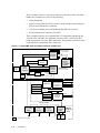
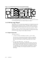
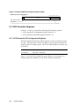
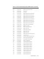
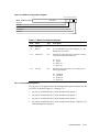
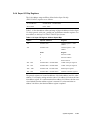
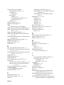
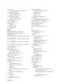
Figure 1–1 identifies the functional components of the Alpha VME 5/352 and
5/480 SBCs. The Alpha VME 5/352 and 5/480 CPU modules are based on the
21164 Alpha microprocessor, and run at 352 MHz and 480 MHz, respectively.
The 21172 core logic chipset consists of the 21172–CA control, I/O interface, and
address (CIA) chip and four 21172–BA data switch (DSW) chips. Nine SRAMs
provide 2 MB of Bcache and two or four main memory DIMMs provide from 16
to 512 MB of EDO memory. The system clock uses a phase lock loop
(PLL)/buffer circuit to provide SYSCLK signals to 10 system components at 32
MHz.
The CPU module interfaces with the I/O module through a 32-bit PCI bus. As
Figure 1–1 shows, the I/O module provides a:
•
PCI-to-VME bridge (DC7407 VIP and VIC64), which provides an interface
to the VMEbus
•
PCI-to-SCSI controller (53C810), which provides an interface to SCSI
devices
•
PCI-to-Ethernet controller (21040), which provides a network interface
•
PCI-to-Nbus bridge (82378ZB), which provides access to the system’s 8-bit
Nbus and includes interrupt controller and interval timer support
•
PCI–32 interface to an optional PMC I/O companion card
Introduction
1–1
The I/O module’s Nbus is a resource bus that is based on the ISA bus. The Nbus
handles the read and write cycles for the following:
•
4M of flash ROM
•
Super I/O chip (FDC37C6656T) resources, which include console and parallel ports and a diskette drive controller
•
TOY clock, watchdog timer, and NVRAM chip (DS1386) resources
•
Keyboard and mouse controller (82C42PE)
The I/O module interfaces to an optional PMC I/O companion card through the
32-bit PCI bus. The PMC I/O companion card uses a DEC 21052 PCI-to-PCI
bridge to provide access to two PMC option slots. This optional card also provides
keyboard, mouse, and diskette drive connectors.
Figure 1–1 Alpha VME 5/352 and 5/480 Functional Components
CPU Module
Memory Data, ECC,
256 or 128 Bits
21172-BA
Data Path
(4 chips)
System Bus Data, ECC, Tag, 128 Bits
352 or
480 MHz
CPU
Clock
21164
Microprocessor
21172-CA
Memory
Controller
and I/O
Interface
System Bus Address, Tag_Dirty, Tag_Ctl
Control
SYSCLK
Main
Memory
(2 or 4)
8 to 128 MB
DIMMs
2 MB
Bcache
Control
Phase
Lock Loop
10
Memory Control
SYSCLK <9:0>
32 MHz
SROM
PCI Bus, 64 Bits
I/O Module
4 MB Flash
S10 Chip 82378ZB
Super I/O
FDC37C6656T
Console and
Parallel Ports
Diskette
Console
Console
Parallel Port
Interrupt Controller
Nbus, 8 Bits
PCI-to-Nbus Bridge
Interval Timer
DS1386
82C42PE
TOY Clock
Watchdog Timer
Keyboard
and Mouse
Controller
Keyboard
Mouse
32 KB NVRAM
PCI Bus, 32 Bits
VIP/VIC64
PCI-to-VME
Bridge
VMEbus
53C510
SCSI
Controller
SCSI
DEC21040
Ethernet
Controller
Ethernet
DEC21052
PCI-to-PCI
Bridge
32
Bits
PMC
Option
Slot 0
PMC I/O
Companion
Card
32
Bits
PMC
Option
Slot 2
= Uses system clock (32 MHz)
ML014166
1–2
Introduction
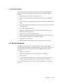
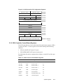
1.2 21164 Alpha Microprocessor
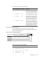
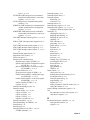
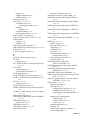
The Alpha VME 5/352 and 5/480 SBCs are based on the 21164 Alpha microprocessor, which is a superscalar pipelined processor manufactured using 0.35 µ m
CMOS technology. It is packaged in a 499-pin IPGA carrier.
The 21164 microprocessor can issue four Alpha instructions in a single cycle,
thereby minimizing the average cycles per instruction (CPI). A number of lowlatency and/or high-throughput features in the instruction issue unit and the
onchip components of the memory subsystem further reduce the average CPI.
The 21164 microprocessor and associated PALcode implements IEEE single-precision and double-precision, VAX F_floating and G_floating data types, and supports longword (32-bit) and quadword (64-bit) integers. Byte (8-bit) and word
(16-bit) support is provided by byte-manipulation instructions. Limited hardware
support is provided for the VAX D_floating data type. Partial hardware implementation is provided for the architecturally optional FETCH and FETCH_M instructions.
Other features of the microprocessor include:
•
An onchip, demand-paged memory-management unit with a translation buffer
•
Two onchip, high-throughput pipelined floating-point units, capable of executing both DIGITAL and IEEE floating-point data types
•
An onchip, 8 KB virtual instruction cache (Icache) with 7-bit ASNs
(MAX_ASN=127
•
An onchip, dual-read-ported, 8 KB data cache (Dcache)
•
An onchip, write buffer with six 32-byte entries
•
An onchip, 96 KB, 3-way, set-associative, write-back, second level (level 2)
mixed instruction and data cache
•
A 128-bit data bus with onchip parity and error correction code (ECC) support
•
Support for an external third level (level 3) synchronous 2 MB backup cache
(Bcache)
•
An internal clock generator providing a high-speed clock used by the 21164
microprocessor, and a pair of programmable system clocks for use by the
CPU module
•
Onchip performance counters to measure and analyze CPU and system performance
•
An Icache test interface to support chip and module level testing
•
A 3.3 V external interface and 2.5 V core power for reduced power consumption
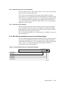
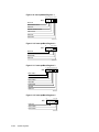
Figure 1–2 shows the microprocessor’s functional units and caches in a functional
block diagram.
Introduction
1–3
Figure 1–2 21164 Alpha Microprocessor Functional Block Diagram
21164
Microprocessor
Instruction
Cache
8 KB
40-Bit Address
Integer
Instruction
Fetch/
Decode
and
Branch
Unit
Integer
Merge
Logic
FPX
FPX
Data Cache
8 KB
Write-Through
SecondLevel
Cache
96 KB
WriteBack
Bus
Interface
Unit
2 MB
Backup
Cache
128-Bit Data
ML014168
For more detailed information on the microprocessor, see the Digital Semiconductor 21164 Alpha Microprocessor Hardware Reference Manual.
1.3 21172 Core Logic Chipset
The DIGITAL 21172 core logic chipset supports the 21164 Alpha microprocessor
in high-performance uniprocessor systems. The chipset includes an interface to
the 64-bit peripheral component interconnect (PCI) bus, and associated control
and data paths for the 21164 microprocessor chip, memory, and level 3 Bcache.
Sections 1.3.1 and 1.3.2 discuss the chipset components and features. For more
detailed information on the 21172 core logic chipset, see the Digital Semiconductor 21172 Core Logic Chipset Technical Reference Manual.
1.3.1 Chipset Components
The chipset consists of:
•
A control, I/O interface, and address (CIA) chip − 21172-CA chip
The CIA chip is a 388-pin plastic ball grid array (PBGA) package that
provides control functions for main memory, a bridge to the 64-bit PCI
bus, and control functions for the DSW chips and part of the I/O data
path.
•
Four data switch (DSW) chips − 21172-BA chips
The DSW chips are 208-pin plastic quad flat pack (PQFP) packages that
provide bidirectional data paths between the 21164 microprocessor, main
memory, Bcache, the CIA chip, and part of the I/O data path. The majority of the DSW logic consists of data buffers and multiplexers. Using two
encoded control fields, the CIA chip directs data flow to and from the
DSW chips.
1–4
Introduction
1.3.2 Chipset Features
The chipset includes the majority of functions required to develop high performance systems that require minimum discrete logic on the module. Features
include:
•
Support for the 21164 Alpha microprocessor chip
•
A 64-bit, ECC-protected data path (IOD bus) between the CIA and DSW
chips
•
A 128-bit ECC-protected data path (system bus) between the 21164 and DSW
chips
•
A 256-bit ECC-protected memory data path (memory bus) between the DSW
chips and memory
•
A 32 MHz system bus interface
•
Support for 2 MB of write-back, ECC-protected, level 3 Bcache using the
flush cache coherency protocol
•
Support for 16 to 512 MB of EDO memory
•
PCI bus support that includes 64-bit multiplexed address and data paths, 64bit PCI address handling, and scatter-gather mapping
•
32 MHz PCI clock frequency
•
DSW chips that provide a victim buffer for read miss/victim transitions
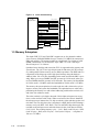
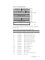
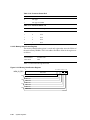
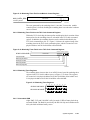
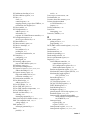
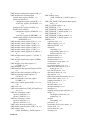
1.4 Bcache Subsystem
The DIGITAL Alpha VME 5/352 and 5/480 SBCs provides 2 MB of direct
mapped Bcache. The Bcache is populated with nine 9 nanosecond, 64K-bit X 36bit synchronous static random access memories (SRAMs). Bcache features
include:
•
A block size of 64 bytes
•
System bus Bcache private read/write transfer rate of 700 MB/s
•
ECC protection
•
Use of the flush cache coherency protocol as described in the Digital Semiconductor 21164 Alpha Microprocessor Hardware Reference Manual
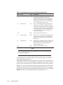
The 21164 Alpha microprocessor controls the level 3 Bcache array as shown in
Figure 1–3.
Introduction
1–5
Figure 1–3 Level 3 Bcache Array
21164
Microprocessor
index_h<20:4>
un_data_ram_oe_h
Bcache
SRAM
un_data_ram_we_h
un_tag_ram_oe_h
un_tag_ram_we_h
index_h<20:6>
tag_data_h<38:30>
Tag
Array
tag_data_h<29:20>
tag_data_par_h
Data
Array
tag_ctl_par_h
tag_valid_h
tag_dirty_h
data_h<127:0>
data_check_h<15:0>
st_clk1_h
idle_bc
Buffer
st_clk1_<9:1>_h
(From CIA Chip)
ML013816
1.5 Memory Subsystem
The Alpha VME 5/352 and 5/480 SBCs support two or four dynamic random
access memory (DRAM) DIMMs for up to a total of 512 MB of 60 nanosecond,
EDO main memory. The memory resides in a single bank. For a listing of valid
DIMM combinations, see the DIGITAL Alpha VME 5/353 and 5/480 SingleBoard Computers User Manual.
Quadword error checking and correction (ECC) is supported on the memory and
system buses. The 21172 core logic chipset controls and routes all CPU-to-memory caching and PCI direct memory access (DMA) operations. The DSW and CIA
components of the chipset provide a high-speed memory data path that has a
width of either 128 or 256 bits, depending on the mode in which the SBC is operating. When you use two DIMMs, the SBC operates in 128-bit mode; when you
use four DIMMs the SBC operates in 256-bit mode. The memory bus bandwidth
in 128-bit mode is 210 MB/s, while the bandwidth in 256-bit mode is 355 MB/s.
The memory subsystem optimizes its cache read miss with victim write cycle to
improve memory and system bus bandwidth. The optimizations are achieved by
partitioning the memory row and column addressing such that the read miss row
and victim row addresses match.
The cache read miss cycle begins when the 21164 Alpha microprocessor recognizes a cache read miss with victim. When a read miss with victim is identified,
the microprocessor instructs the CIA chip to take the victim and then get the read
miss data. The CIA chip places the victim data in a DSW buffer while initiating a
memory read cycle (RAS–CAS–RAS). The CIA and DSW chips then supply the
read data to the microprocessor and cache then write the victim data to memory
(CAS–CAS). The resulting memory cycle — CAS – RAS (read 32 bytes) – RAS
(read 32 bytes) – RAS (write 32 bytes) – RAS (write 32 bytes) — completes in
360 ns or 355 MB/s.
1–6
Introduction
1.6 SROM
The SROM for the Alpha VME 5/352 and 5/480 SBCs contains 8 KB of code that
is loaded into the Alpha 21164 microprocessor’s Icache serially when the system
powers up or during a reset. Execution is passed to this code in PAL mode. SROM
initialization is explained in detail in the DIGITAL Alpha VME 5/352 and 5/480
Single-Board Computers User Manual.
The SROM is socketed to allow future firmware upgrades.
1.7 Clock Interface
The CPU clock circuit used by the Alpha VME 5/352 and 5/480 SBCs multiplies
a 16 MHz clock frequency by 22 or 30 and buffers the results, supplying the
Alpha 21164 microprocessor with a 352 MHz or 480 MHz clock speed. The
microprocessor divides the input value 352 or 480 by 11 or 15, respectively, to
generate the system clock.
The 21164 system clock signal (SYSCLK) drives a phase lock loop (PLL)/buffer
circuit. That circuit, in turn, generates 10 copies of the 32 MHz SYSCLK signal
for the 21172 core logic chipset components and all PCI devices.
The 21172 core logic chipset generates its own 1x and 2x clock signals on each
DSW and CIA chip.
1.8 PCI Interface
The PCI interface consists of a PCI bus that serves as the base of the I/O subsystem, connecting all of the system’s PCI devices. The I/O subsystem consists of
the 21172 core logic CIA and DSW chips and the following PCI devices:
•
Ethernet controller
•
SCSI controller
•
PMC I/O companion card
•
Nbus interface
•
VME interface
Sections 1.8.1 to 1.8.3 briefly discuss Ethernet, SCSI, and PCI Expansion Card
support. For introductions to the Nbus and VME interfaces, see Sections 1.9 and
1.10.
1.8.1 Ethernet Controller
The Ethernet controller for the Alpha VME 5/352 and 5/480 SBCs is based on the
DECchip 21040-AA. This chip keeps processor intervention in local area network
(LAN) control to a minimum. The chip behaves:
•
As a bus slave when communicating with the PCI bus to gain access to configuration and control/status registers
•
As a bus master when communicating with memory
The Ethernet controller handles the following types of cycle termination:
Introduction
1–7
•
Target-initiated retry
•
Abort
•
DEVSEL abort
Target-aborted terminations cause an interrupt.
The physical connection to the network is through the Ethernet 10BASE–T
twisted-pair connector located on the front panel of the CPU and I/O subassembly.
The Ethernet ID address for the Alpha VME 5/352 or 5/480 SBC assembly is
stored in a 20-pin socketed PLCC.
For more information on programming and using the DECchip 21040-AA, see the
DECchip 21040-AA Specification.
1.8.2 SCSI Controller
The SCSI controller for the Alpha VME 5/352 and 5/480 SBCs is based on the
Symbios 53C810 chip. This controller allows you to attach up to seven SCSI
devices to your SBC.
The primary breakout module (5424663) provides an interface to a standard SCSI
cable. This module brings the SCSI bus to a standard 50-pin SCSI IDC connector
pinning for direct connection to an unshielded SCSI cable. A 6-pin jumper block
on the module controls SCSI termination as follows:
•
Enables SCSI termination when the jumper is set across pins 1 and 3
•
Disables SCSI termination when the jumper is set across pins 3 and 5
The controller can affect high-level SCSI operations with very little intervention
from the processor. The controller accomplishes this through its low-level register
interface or by applying Symbios SCSI scripts.
Once the controller is configured in PCI address space, programming of the Symbios 53C810 chip is compatible with the Symbios 53C720 chip.
For more information on programming the Symbios 53C720 chip, see the chip’s
programming guide.
1.8.3 PMC I/O Companion Card
The optional PMC I/O companion card provides a 21052 PCI-to-PCI bridge chip
and two sets of PMC connectors for adding one double-width or two single-width
PMC option modules. One of the PMC connector sets includes a third connector
that allows I/O access through the P2 connector.
PCI bus arbitration supports two PMC devices with up to four interrupt request
lines. The PCI clock is driven from the CPU and I/O subassembly at a frequency
of 32 MHz. The card connectors provide 3V and 5V supply voltages. Although
you can have mixed supply voltages between cards, the PCI bus signaling voltage
must be configured to 5V when the card is installed.
1–8
Introduction
1.9 Nbus Interface
The Nbus interface is a simple nonmultiplexed resource bus that is based on the
ISA bus and supports 8-bit data transfers and 16-bit addressing. This bus provides
an interface to the PCI bus through an Intel System I/O chip (82378ZB). The
interface translates PCI I/O references to the Nbus into simple read and write
cycles for resources attached to the Nbus lines. Such resources include the system’s:
•
Interrupt controllers
•
Flash ROM
•
TOY clock
•
Watchdog timer
•
NVRAM
•
Interval timer
•
Keyboard and mouse controller
•
Super I/O chip
1.9.1 Interrupt Controllers
Most interrupts on Alpha VME 5/352 and 5/480 SBCs are routed through the following interrupt controllers:
•
Xilinx interrupt controller
•
VIC64 chip system interrupt controller
•
SIO chip (82378ZB) programmable interrupt controller
The Xilinx interrupt controller handles CPU interrupts. This controller consists of
four interrupt mask registers that generate CPU interrupt request signals.
The VIC64 chip interrupt controller handles VMEbus interrupts. It controls two
external/system interrupt sources: DC7407 status and DC7407 errors. Each of
these sources has an associated interrupt control register (ICR) that allows the
interrupt to be programmed with an interrupt priority level (IPL) or disabled.
Use of the VIC64 chip in Alpha VME 5/352 and 5/480 SBCs as an interrupt controller is modified slightly by the operation of the DC7407, the SIO chip, and the
interrupt/mask registers.
The SIO chip interrupt controller delivers interrupts from the mouse, keyboard,
and Super I/O chip (FDC37C6656T) to the interrupt/mask register.
For more information about the interrupt controllers and the handling of system
interrupts, see Chapter 4.
Introduction
1–9
1.9.2 Flash ROM
The Alpha VME 5/352 and 5/480 SBCs have a total of 4 MB of electrically erasable and writable flash ROM. The flash ROM is segmented into 1 MB windows,
using bits <1:0> of a module control register. The system console firmware is prewritten into the first 512 KB, providing you with 3.5 MB of additional space to
use for your application.
To protect the contents of the flash ROM from unauthorized or accidental updates,
you must close DIP Switch 2 on the I/O module before enabling write operations.
That switch must always be open unless you are updating the flash ROM. (The
state of the switch is stored in Flash Switch bit <3> of the module control register.) Independent of the state of the switch, you can overwrite the setting in the
software to enable automatic updates.
1.9.3 TOY Clock
The Dallas Semiconductor DS1386 chip provides the SBC’s time-of-year (TOY)
clock functionality. This chip also supports the watchdog and SRAM functionality
as nonvolatile random access memory (NVRAM).
Note
The Alpha VME 5/352 and 5/480 SBCs do not support the DS1386 chip’s
alarm features.
The TOY clock maintains the system’s time: year, month, date, day, hour, minute,
second, 110th of a second, and 1/100th of a second. The clock corrects the date for
months with fewer than 31 days and for leap years. In addition, the clock can
maintain the time in 24-hour or 12-hour AM/PM format.
The square wave output of the chip generates a fixed 1024 Hz interval and timekeeping accuracy is better than +/- minute/month at 25 ° C.
The clock maintains time in the absence of Vcc by using an internal lithium (less
than 0.5 grams) energy cell that has an active life of at least 10 years. In addition,
internally the clock protects against spurious accesses during power transitions.
Some applications may require the TOY clock and NVRAM to operate from an
external uninterruptable power supply (UPS). The Alpha VME 5/352 and 5/480
SBCs have an onboard switch (J3 switch 1) to allow a connection to the 5 V
standby connection (5VSTDBY) on the VMEbus. When Switch 1 is closed, the
VME 5VSTDBY is connected to the TOY supply through isolation diodes.
The chip is socketed to allow:
•
Replacement when the internal power source is no longer functional
•
Physical removal of the NVRAM
The TOY clock registers are updated every 0.01 seconds. You gain access to the
clock to examine or set the current time by using the console date command (see
the DIGITAL Alpha VME 5/352 and 5/480 Single-Board Computers User Manual).
1–10
Introduction
1.9.4 Watchdog Timer
The watchdog timer resides on the Dallas Semiconductor DS1386 chip. The
watchdog timer allows hardware to bring the system back to a known state when a
software failure occurs.
An application can initialize the watchdog timer with a value in the range 0.01 to
99.9 seconds. If left unaccessed, the timer decrements towards 0. If the timer
reaches 0, the watchdog timer halts the system (jump to Halt entry in firmware)
and then forces the module hardware to be reset (some 300 ms later). The application can maintain the module by periodically accessing the watchdog timer registers. When you access these registers, the watchdog timer resets back to the
initialization value. Therefore, as long as the worst-case time between watchdog
timer access is less than the programmed timeout value, the module functions normally.
The Alpha VME 5/352 and 5/480 SBCs indicate the status of the on-board watchdog timer with the signal WD_STATUS_OC on pin C6 of the VME P2 connector.
This signal is driven low when an on-board watchdog timer expires. The device
that drives the signal is a 74LS05 open-collector inverter. This device is capable
of sinking the signal a maximum of 8 mA (IOL). You can pull up the
WD_STATUS_OC signal to the 5 V rail by using a 2 K Ω resistor and setting the
primary breakout module jumper across pins 4 and 6 (default). To disconnect the
resistor from the 5 V rail, set the jumper across pins 2 and 4.
In addition to the hardware support for watchdog timer operation, you can configure the firmware to dispatch to user code or continue with its default reset action
on watchdog timeout. The firmware can detect the expiration of the watchdog
timer during a reset operation by examining the hardware reset reason register.
The jump to the Halt code just before the reset enables the firmware to record a
snapshot of the processor’s state before the hardware reset is complete.
1.9.5 NVRAM
Within the TOY clock, the Alpha VME 5/352 and 5/480 SBCs offer just under 32
KB of on-board SRAM that is backed up by battery. The RAM is provided by the
Dallas Semiconductor DS1386 chip and is held nonvolatile by a built-in lithium
battery source.
The nonvolatile RAM (NVRAM) is accessible for read and write operations in
Nbus space. The DS1386 chip contains 32 KB read/write byte elements. The lowest 14 of these bytes have special register functions for operation of the TOY
clock and watchdog timer. You can use the remaining bytes, 32754 bytes, as general-purpose bytewide read/write RAM.
1.9.6 Interval Timer
The interval timer for the Alpha VME 5/352 and 5/480 SBCs is based on the
82C54 chip. On power up, the 82C54 chip is in an undefined state and must be initialized before being used. For information on timers, timer modes, or how to use
the chip, see Section 5.4.6.
Introduction
1–11
1.9.7 Keyboard and Mouse Controller
The keyboard and mouse controller is provided by an Intel 82C42PE single-chip
microcomputer. The controller is programmed to be IBM PC/AT compatible and
can drive the keyboard and PS/2 type mouse supported by DECpc systems. The
keyboard and mouse ports are female 6-pin mini-DIN, PS/2 type connectors. The
controller is programmed to allow either device to operate in either port.
1.9.8 Super I/O Chip
The FDC37C665GT Super I/O chip (not to be confused with the standard I/O, or
SIO, chip) supports serial-line port channels A and B (16550 UARTS) and a parallel port. It provides first-in-first-out (FIFO) data access for the serial ports and
EPP/ECP modes for the parallel port.
The Alpha VME 5/352 and 5/480 SBCs use channel A for the console. The firmware configures this channel as an asynchronous line, using baud rate, parity, data
bit, and stop bit configuration data that you define and is stored in NVRAM. If
NVRAM does not contain valid data on power-up, the SBC configures channel A
with defaults of 9600 baud, no parity, eight bits, and one stop bit.
The system firmware does not commit or initialize channel B.
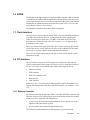
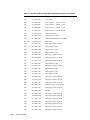
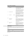
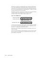
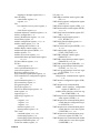
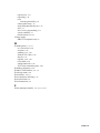
1.10 VME Interface
The PCI-to-VME interface for the Alpha VME 5/352 and 5/480 SBCs conforms
to the IEC 821, IEEE1014–1987, and D64 sections of IEEE1014 Rev.D (draft)
standards. The interface is implemented using the following components:
•
VIP ASIC (DC7047B) chip
•
The Cypress Semiconductor VIC64 VMEbus interface chipset
•
Three CY7C964 bus interface chips
•
Static scatter-gather RAM for address mapping
•
Support logic implemented with programmable logic devices (PLDs)
The VIP/VIC64 chip combination accepts and generates VMEbus D08, D16,
D32, and D64 data transfers and protocols. The chip combination supports
addressing modes A16, A24, and A32 as a master or slave on the VMEbus.
The VIP chip uses information stored in the scatter-gather RAM to perform bigto-little endian data translation (byte swapping) and address mapping when data
moves to and from the VMEbus.
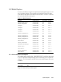
Figure 1–4 shows the interface components and the address and data paths
between them.
1–12
Introduction
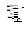
Figure 1–4 PCI-to-VME Interface Components
VIP
VIP Registers
Scatter/Gather
RAM
PCI Bus
A<31:0> D<31:0> A<27:13> D<31:5>
VIC64
A<7:0>
<A<31:0>
D<7:0>
<D<31:0>
VIC CSRs
CY7C964
A,D<31:24>
VME_A,D
<31:24>
CY7C964
A,D<23:16>
VME_A,D
<23:16>
CY7C964
A,D<15:8>
VME_A,D
<15:8>
VME_A,D<7:0>
VME_D[31:0]
VME_A[31:1]
ML014167
1.10.1 VIP Chip
The VIP chip controls the 32-bit wide PCI bus. Its PCI configuration registers
allow it to function as the PCI bus target and initiator. The VIP chip:
•
Functions as a PCI slave to all processor I/O read and write operations that
target the VIP registers, the CY7C964 chip registers, the scatter/gather RAM,
or VME memory space
•
Responds to PCI interrupt acknowledge cycles when set up as the PCI interrupt responder
•
Functions as a PCI master in response to the VIC64 chip requesting data from
or sending data to PCI memory
•
Performs address translation between the PCI bus and the VMEbus for transfers to and from the VMEbus
1.10.2 VIC64 and CY7C964 Chips
The VIC64 and CY7C964 chips control the VMEbus. The VIC64 chip functions
as a VMEbus slave in response to VME addresses that match those set up by the
address base and address base mask registers. This chip functions as VMEbus
master:
•
In response to the processor reading from and writing to VME memory (programmed I/O)
•
To execute DMA transactions (master block transfers) set up by the processor
in the VIP/VIC64 interface
Introduction
1–13
For more information on the VIC64 and CY7C964 chips, see the Cypress Semiconductor VIC068 User’s Guide, VIC64 design notes, and CY7C964 User’s
Guide.
1.10.3 Address Mapping and the Scatter-Gather Map
The VIP chip translates addresses by using a mapping table in scatter-gather RAM
called the scatter-gather map. The scatter-gather map translates addresses for outbound and inbound VMEbus transactions.
For outbound transactions, the VIP chip maps a 512 MB region of PCI memory
space to the VMEbus. The outbound scatter-gather map translates a maximum of
2K naturally aligned 256 KB pages within that 512 MB region to 256 KB of naturally aligned pages on the VMEbus (A32, A24, or A16). A PCI address is used as
an index into the scatter-gather map to give the corresponding VME address.
For inbound transactions, the VIP chip maps naturally aligned 8 KB regions of
VMEbus A32 and A24 address spaces to naturally aligned 8 KB regions of PCI
address space (memory or I/O). The inbound scatter-gather map consists of two
parts. One part translates up to 2K pages (8 KB) of VMEbus A24 address space to
8 KB pages of PCI address space. The other part maps up to 16K pages (8 KB) of
VMEbus A32 address space to 8 KB pages of PCI address space. An incoming
VME address is used as the index to select the PCI address.
The scatter-gather map may be accessed from the PCI bus (written to or read
from) under VIP control. Scatter-gather entries also contain information to control
inbound accesses and byte swapping.
The VIP chip contains a single entry scatter-gather cache and a set of registers.
The cache stores the last accessed outbound scatter-gather entry and its corresponding scatter-gather address index. The registers provide mapping for inbound
and outbound transactions (one mapping in each direction).
For more information about VME interface address mapping, see Chapter 2.
1–14
Introduction
2
System Address Mapping
The CIA chip of the 21172 core logic chip set manages system address mapping
for Alpha VME 5/352 and 5/480 SBCs. The chip maps 40-bit physical addresses
of the 21164 microprocessor to memory and I/O space addresses.
This chapter discusses DIGITAL Alpha VME 5/352 and 5/480 SBC support for
the 21172 core logic chipset. The chapter provides an address space overview
(Section 2.1) and describes:
•
PCI dense memory space, Section 2.2
•
PCI sparse memory space, Section 2.3
•
PCI sparse I/O space, Section 2.4
•
PCI configuration space, Section 2.5
•
Byte/word PCI space, Section 2.6
For details about 21172 core logic chipset address mapping, see the Digital Semiconductor 21172 Core Logic Chipset Technical Reference Manual.
2.1 Address Space Overview
Sections 2.1.1 through 2.1.3 provide an overview of Alpha VME 5/352 and 5/480
SBC address space by discussing:
•
Cached and noncacheable regions, Section 2.1.1
•
Supported address spaces, Section 2.1.2
•
21164 address space mappings, Section 2.1.3
2.1.1 Cached and Noncacheable Regions
The address space of the 21164 microprocessor is divided into two regions:
cached memory and noncacheable address space. Figure 2–1 shows these regions
as they are mapped with the 21172 core logic chipset support.
Figure 2–1 21164 Microprocessor Address Space
00.0000.0000
Cached Memory
01.FFFF.FFFF
02.0000.0000
Reserved
7F.FFFF.FFFF
80.0000.0000
Noncacheable Address Space
8B.FFFF.FFFF
LJ04259A.AI
System Address Mapping
2–1
The region of the address space that is accessible to the microprocessor at any
given time is determined by physical address bit addr<39>. When this bit is clear,
the microprocessor has access to cacheable memory (partly reserved). When the
bit is set, the microprocessor has access to noncacheable address space. The system uses noncacheable address space for:
•
PCI address space mapped to memory
•
PCI I/O space
•
PCI configuration information
•
Special/interrupt acknowledge cycles
•
CIA control/status registers (CSRs)
•
Flash ROM and support logic registers
2.1.2 Supported Address Spaces
The CIA chip supports the following address spaces:
•
The first 8 GB of cached memory space
•
Noncacheable memory space mapped for I/O devices
The remainder of the cached memory space is reserved. The block size for the
cached memory space is 64-bytes. The CIA chip sends READ and FLUSH commands to the microprocessor’s caches for direct-memory access (DMA) traffic to
the 8 GB of cached memory address space.
Within the noncacheable memory space, the Alpha VME 5/352 and 5/480 SBC
firmware implements the following address spaces:
Address Space
Firmware
Implementation
PCI dense memory space
2 GB
PCI sparse memory space
128 MB
PCI sparse I/O space
16 MB
PCI configuration space
4 GB
Figure 2–2 shows the 21164 address space configuration as supported by the
Alpha VME 5/352 and 5/480 SBCs.
2–2
System Address Mapping
Figure 2–2 21164 Address Space Configuration
80.0000.0000
85.8000.0000
Reserved for SIO
Reserved
85.8001.FFFF
80.000F.FFF
85.8000.8000
80.0010.0000
DS1386
(TOY Clock, NVRAM)
VIP Control/Status Registers
85.8008.0000
80.0020.0000
VIP/VME Scatter-Gather Programmed by Firmware
80.0022.0000
SCSI Controller Programmed by Firmware
80.0022.0100
Ethernet Controller Programmed by Firmware
Interval Timer
21164 Address Space
00.0000.0000
Cached Memory
01.FFFF.FFFF
02.0000.0000
Reserved
VIP/VME Window Programmed by Firmware
SCSI Programmed by Firmware
7F.FFFF.FFFF
80.0000.0000
80.1800.0000
Ethernet Programmed by Firmware
PCI Sparse Memory Space
PMC Option Programmed By Firmware
85.7FFF.FFFF
85.8000.0000
PCI Sparse I/O Space
PMC Option Slots Programmed by Firmware
85.FFFF.FFFF
86.0000.0000
PCI Dense Memory Space
86.FFFF.FFFF
87.0000.0000
86.0000.0000
Flash ROM
86.000F.FFFF
86.0010.0000
Not used by Firmware
86.7FFF.FFFF
86.8000.0000
VIP/VME Window
86.9FFF.FFFF
86.A000.0000
PCI Dense Memory Space Programmed by Firmware
PCI Configuration Space
87.FFFF.FFFF
88.0000.0000
PCI Byte/Word Space
8B.FFFF.FFFF
87.0000.0000
DC7047 VIP Chip
87.0000.00FF
87.0001.0000
DEChip 21040 Ethernet
87.0001.00FF
87.0002.0000
Symbios 53810 SCSI
87.0002.00FF
87.0003.0000
Intel 82378 SIO Chip
87.0003.00FF
87.0004.0000
PMC Module
87.0004.00FF
87.2000.0000
Reserved for CIA Chip
87.7FFF.FFFF
86.FFFF.FFFF
System Address Mapping
2–3
Table 2–1 shows how the Alpha VME 5/352 and 5/480 SBC firmware implements
the 21164 physical address space mappings.
Table 2–1 21164 Physical Address Space Mappings
Physical Address Range
Description
Firmware
Implementation
00.0000.0000 – 01.FFFF.FFFF
Cached memory
8 GB
02.0000.0000 – 7F.FFFF.FFFF
Reserved
80.0000.0000 – 85.7FFF.FFFF
PCI sparse memory space
80.0000.0000 – 80.000F.FFFF
PCI sparse memory space – Reserved
80.0010.0000
PCI sparse memory space – VIP control/status regis- 512 Bytes
ters
80.0020.0000
PCI sparce memory space – VIP/VME ScatterGather –
programmed by firmware
80.0022.0000
PCI sparse memory space – SCSI controller –
programmed by firmware
80.0022.0100
PCI sparse memory space – Ethernet controller –
programmed by firmware
80.1800.0000
PCI sparse memory space – VIP/VME Window –
programmed by firmware
128 MB
128 KB
64 MB
PCI sparse memory space – PMC Option Slots –
programmed by firmware
85.8000.0000 – 85.FFFF.FFFF
PCI sparse I/O space
85.8000.0000 – 85.8001.FFFF
PCI sparse I/O space – Reserved for SIO
85.8000.8000
PCI sparse I/O space – DS1386 (TOY Clock,
NVRAM)
85.8008.0000
PCI sparse I/O space – Interval timer
85.8001.0000 – 85.8100.0000
PCI sparse I/O space –
programmed by firmware
16 MB - 64 KB
86.0000.0000 – 86.FFFF.FFFF
PCI dense memory space
2 GB
86.0000.0000 – 86.000F.FFFF
PCI dense memory space – Flash ROM
1 MB
86.0010.0000 – 86.7FFF.FFFF
PCI dense memory space – Not used by firmware
86.8000.0000 – 86.9FFF.FFFF
PCI dense memory space – VIP/VME Window
512 MB
86.A000.0000 – 86.FFFF.FFFF
PCI dense memory space – programmed by firmware
1.5 GB
87.0000.0000 – 87.FFFF.FFFF
PCI configuration space
4 GB
87.0000.0000 – 87.0000.00FF
PCI configuration space – DC7407 VIP chip
87.0001.0000 – 87.0001.00FF
PCI configuration space – DECchip 21040 Ethernet
87.0002.0000 – 87.0002.00FF
PCI configuration space – Symbios 53810 SCSI
87.0003.0000 – 87.0003.00FF
PCI configuration space – Intel 82378 SIO chip
2–4
System Address Mapping
16 MB
Table 2–1 21164 Physical Address Space Mappings (Continued)
Firmware
Implementation
Physical Address Range
Description
87.2000.0000 – 87.7FFF.FFFF
PCI configuration space – Reserved for CIA chip
88.0000.0000 – 8B.FFFF.FFFF
Byte/word PCI space1
88.0000.0000 – 88.FFFF.FFFF
Byte/word PCI memory space1
89.0000.0000 – 89.FFFF.FFFF
Byte/word PCI I/O space1
8A.0000.0000 – 8A.FFFF.FFFF
Byte/word PCI configuration space – type 0 1
8B.0000.0000 – 8B.FFFF.FFFF
Byte/word PCI configuration space – type 11
1
Not used by the firmware, but available for use by operating systems.
Note
The results of gaining access to address space outside the physical address
ranges shown in Table 2–1 are undefined.
2.1.3 21164 Address Space
The 21164 microprocessor address space consists of 17 address regions that range
in size from 0.25 GB to 16 GB. Sections 2.2 through 2.6 describe the following
address regions:
•
PCI dense memory space, Section 2.2
•
PCI sparse memory space, Section 2.3
•
PCI sparse I/O space, Section 2.4
•
PCI configuration space, Section 2.5
•
PCI byte/word space, Section 2.6
2.2 PCI Dense Memory Space
PCI dense memory space is typically used for PCI data buffers, such as video
frame buffers or nonvolatile RAM (NVRAM). The Alpha VME 5/352 and 5/480
SBC firmware implements PCI dense memory space in the address range
86.0000.0000 to 86.7FFF.FFFF.
Sections 2.2.1 to 2.2.6 discuss the following:
•
Dense memory space characteristics, Section 2.2.1
•
Advantages of dense memory space over sparse memory space, Section 2.2.2
•
Dense memory space address generation, Section 2.2.3
•
Flash ROM address mapping, Section 2.2.4
•
VME address mapping in dense memory space, Section 2.2.5
•
How to gain access to dense memory space, Section 2.2.6
System Address Mapping
2–5
2.2.1 Characteristics
Dense memory space is provided for the 21164 microprocessor to gain access to
PCI memory space, but not PCI I/O space. Dense memory space has the following
characteristics:
•
A one-to-one mapping exists between 21164 microprocessor addresses and
PCI addresses. A 21164 microprocessor longword address maps to a longword on the PCI with no shifting of the address field.
•
The concept of dense memory space (and sparse space) is applicable only to
addresses generated by the 21164 microprocessor. The PCI bus does not generate dense memory space (or sparse space).
•
Access to a byte or word is not possible in dense memory space. The minimum access granularity is a longword on write transactions and a quadword
on read transactions. The maximum transfer length is 32 bytes (performed as
a burst of 8 longwords on the PCI bus). Any combination of longwords may
be valid on write transactions. Valid longwords surrounding invalid longwords (called a “hole”) must be handled correctly by all PCI devices. The
CIA chip allows such “holes” to be issued.
•
Read transactions consist of a burst of two or more longwords on the PCI bus
because the minimum granularity is a quadword. The microprocessor can
request a longword but the CIA chip always fetches a quadword, thus
prefetching a second longword. Therefore, you cannot use dense memory
space for devices that generate side effects when performing a read transaction. Although a longword may be prefetched, the prefetch buffer is not
treated as a cache and thus coherency is not an issue. A quadword read transaction is not atomic on the PCI bus. That is, the target device is at liberty to
force a retry after the first longword of data is sent, and then allow another
device to take control of the PCI bus. The CIA chip does not drive the PCI
lock signal and thus the PCI bus cannot ensure atomicity. This is true of all
current Alpha systems using the PCI bus.
•
The 21164 microprocessor merges noncached read transactions up to a 32byte maximum. The largest dense memory space read transaction from the
PCI bus is 32 bytes.
•
Write transactions to dense memory space are buffered in the 21164 microprocessor. The CIA chip supports a burst length of 8 on the PCI bus, corresponding to 32 bytes of data. In addition, the CIA chip provides four 32-byte
write buffers to maximize I/O write performance. These four buffers are
strictly ordered.
2.2.2 Advantages Over Sparse Space
Dense memory space does not allow byte or word access but has the following
advantages over sparse space:
•
Contiguous memory locations
Some software requires PCI transactions to be at adjacent 21164
addresses, instead of being widely separated as in sparse space.
2–6
System Address Mapping
•
Higher bus bandwidth
PCI bus burst transfers are not usable in sparse space except for a 2-longword burst for quadword write transactions. Dense memory space is
defined to allow both burst read and write transactions.
•
Efficient read/write buffering
In sparse space, separate transactions use separate read or write buffer
entries. Dense memory space allows separate transactions to be collapsed
in read and write buffers.
•
Few memory barriers
In general, transactions that gain access to sparse space are separated by
memory barriers to avoid read/write buffer collapsing. Transactions that
gain access to dense memory space only require barriers when the software requires explicit ordering.
2.2.3 Address Generation
For information on address generation in dense memory space, see the Digital
Semiconductor 21172 Core Logic Chipset Technical Reference Manual.
2.2.4 Flash ROM Address Mapping
The flash ROM maps to dense memory space. Figure 2–3 shows the system has a
total of 4 MB of flash ROM, which is divided into four 1 MB segments. The
21164 and PCI dense memory addresses for this memory space are as follows:
Address Type
Physical Address Range
21164
86.0000.0000 – 86.0007.FFFF
PCI dense memory
ROM_BASE_ADDR = 0000.0000
Figure 2–3 Flash ROM Layout/Addressing
ROM_BASE_ADDR :
<00>
Start of Console Firmware
512 KB
Start of User Flash
512 KB
<01>
1 MB
<10>
1 MB
<11>
1 MB
ML013291
Only byte accesses to the ROM are supported. As Figure 2–3 shows, the first 512
KB of flash ROM are reserved for console firmware use. The remaining space in
the flash ROM is reserved for onboard user code.
System Address Mapping
2–7
You can control and gain access to the flash ROM by using the module control
register 1 (MOD_CNTRL_REG_1). For a description of this register, see Section
5.4.3.7.
2.2.5 VME Address Mapping
Alpha VME 5/352 and 5/480 SBCs support VME address spaces A16, A24, and
A32, using two address windows to map from PCI memory space to VME address
space. One of the address windows, VME_WINDOW_1, maps from PCI dense
memory space. This 512 MB address window is divided into 2048 X 256 KB
pages. Each page is mapped to VME address space by its own scatter-gather entry.
The entries of the first 256 pages are also used to map pages of the second address
window, VME_WINDOW_2, which allows access to PCI sparse memory space.
For information on how VME_WINDOW_2 maps to PCI sparse memory space,
see Section 2.3.3. For more detail on VME address mapping, see Section 3.2.
2.2.6 Gaining Access to PCI Dense Memory Space
To gain access to PCI dense memory space, specify a dense space address with the
examine console command as follows:
>>>examine pmem:address
For example:
>>>examine pmem:8600000000
2.3 PCI Sparse Memory Space
PCI sparse memory space maps a large piece of 21164 memory address space to a
small PCI address space. For example, a 32-byte memory address might map to a
1-byte PCI address. The Alpha VME 5/352 and 5/480 SBC firmware implements
PCI sparse memory space in the address range 80.0000.0000 to 80.07DF.FFFF.
A problem arises because the Alpha instruction set can express only ALIGNED
longword and quadword data references. The PCI bus requires the ability to
express byte, word, tribyte, longword, and quadword references. The CIA must
also be able to emulate PCI transactions for PCI devices designed for systems that
are capable of generating the UNALIGNED references.
The CIA chip accomplishes UNALIGNED PCI references by encoding the size of
the data transfer (byte, word, and so on) and the byte-enable information in
address bits addr<6:3> of the 21164 address. The PCI longword address bits
ad<26:3> are generated by using the remaining address bits addr<31:7>.
For information on quadword address encoding, see the Digital Semiconductor
21172 Core Logic Chipset Technical Reference Manual.
Sections 2.3.1 to 2.3.4 discuss the following:
2–8
•
Low-order address bits in sparse memory space, Section 2.3.1
•
High-order address bits in sparse memory space, Section 2.3.2
•
VME address mapping in sparse memory space, Section 2.3.3
System Address Mapping
•
How to gain access to sparse memory space, Section 2.3.4
2.3.1 Low-Order Address Bits
Low-order PCI sparse memory space address bits addr<7:3> generate the length
of the PCI bus transaction in bytes and are used for byte enables and ad<2:0>.
Address bits addr<30:8> correspond to the quadword PCI address and are sent on
the PCI bus as ad<25:3>.
For more information on the low-order address bits for PCI sparse memory space,
see the Digital Semiconductor 21172 Core Logic Chipset Technical Reference
Manual.
2.3.2 High-Order Address Bits
High-order PCI sparse memory space address bits ad<31:26> are obtained from
the hardware address extension register (HAE_MEM) or the 21164 address,
depending on sparse space regions.
For more information on the high-order address bits for PCI sparse memory
space, see the Digital Semiconductor 21172 Core Logic Chipset Technical Reference Manual.
2.3.3 VME Address Mapping
Alpha VME 5/352 and 5/480 SBCs support VME address spaces A16, A24, and
A32, using two address windows to map from PCI memory space to VME address
space. One of the windows, VME_WINDOW_2, allows mapping to PCI sparse
memory space. This 64 MB address window is divided into 256 X 256 KB pages.
The pages are mapped by the same scatter-gather entries that map the first 256
pages in VME_WINDOW_1 (see Section 2.2.5).
For more detail about VME address mapping, see Section 3.2.
2.3.4 Gaining Access to PCI Sparse Memory Space
To gain access to PCI sparse memory space, specify a sparse space address with
the examine console command as follows:
>>>examine pmem:address
For example:
>>>examine pmem:8000000000
For rules on gaining access to PCI sparse memory space, see the Digital Semiconductor 21172 Core Logic Chipset Technical Reference Manual.
System Address Mapping
2–9
2.4 PCI Sparse I/O Space
PCI sparse I/O space has characteristics similar to the PCI sparse memory space.
A read or write transaction to this space causes a PCI I/O read or write transaction.
The Alpha VME 5/352 and 5/480 SBC firmware implements PCI sparse I/O space
in the address range 85.8000.0000 to 85.80FF.FFFF.
Note
All devices on the Nbus reside in PCI sparse I/O space.
Sections 2.4.1 to 2.4.4 discuss the following:
•
High-order address bits in sparse I/O space, Section 2.4.1
•
Sparse I/O space address decoding, Section 2.4.2
•
Generation of sparse I/O space addresses, Section 2.4.3
•
How to gain access to sparse I/O space, Section 2.4.4
2.4.1 High-Order Address Bits
High-order PCI sparse I/O space address bits addr<34:30> are equal to 101102.
These bits address the lower 32 MB of PCI sparse I/O space. Bits ad<31:25> are
set to zero by the hardware.
For more information on the high-order address bits for PCI sparse I/O space, see
the Digital Semiconductor 21172 Core Logic Chipset Technical Reference Manual.
2.4.2 Address Decoding
PCI sparse I/O space regions are negatively decoded and are not affected by
another PCI device that is programmed to positively decode PCI addresses.
2.4.3 Address Generation
For information on PCI sparse I/O space address generation, see the Digital Semiconductor 21172 Core Logic Chipset Technical Reference Manual.
2.4.4 Gaining Access to PCI Sparse I/O Space
To gain access to PCI sparse I/O space, specify a PCI I/O space address with the
examine console command as follows:
>>>examine pciio:address
For example:
>>>examine pciio:8580000000
2–10
System Address Mapping
2.5 PCI Configuration Space
The PCI configuration register set occupies PCI configuration space. The Alpha
VME 5/352 and 5/480 SBC firmware implements PCI configuration space in the
physical address range 87.0000.0000 to 87.1FFF.FFFF.
The base address of each PCI device, except the Nbus interface (SIO), is configured by the system firmware. The firmware initializes each base address by writing the configuration registers that are in the PCI configuration space.
Note
Software designers should clear CIA_CTRL[FILL_ERR_EN] when
probing for PCI devices using configuration space read transactions. This
prevents the CIA chip from generating an ECC error if no device
responds to the configuration cycle and UNPREDICTABLE data is read
from the PCI bus.
Sections 2.5.1 to 2.5.3 discuss the following:
•
Device type selection, Section 2.5.1
•
Configuration space address generation, Section 2.5.2
•
CIA chip registers, Section 2.5.3
•
How to gain access to configuration space, Section 2.5.4
2.5.1 Device Type Selection
A CPU read or write transaction to PCI configuration address space causes a configuration read or write cycle on the PCI bus. Each transaction is associated with
one of two types of target devices defined as follows:
Type
Target Devices
0
Devices on the primary 64-bit 21164 system PCI bus.
1
Devices on the secondary 32-bit 21164 system PCI bus (that is, behind a PCIto-PCI bridge).
As shown in Figure 2–4, the value of the configuration register determines the target device type. To select Type 0 target devices, set bits CFG<1:0> equal to 002.
To select Type 1 target devices, set the bits to 012.
Note
Bits CFG<1:0> set to 102 and 112 are reserved by the PCI specification.
System Address Mapping
2–11
Figure 2–4 PCI Configuration Space Definition
CPU Address
39 38
1
35 34
MBZ
32 31
29 28
21 20
16 15
13 12
07 06 05 04 03 02
00
1 1 1 0 0 0
Length
Byte Offset
CFG<1:0>
Type 0 PCI
Configuration
Address
Type 1 PCI
Configuration
Address
31
11 10
IDSEL
31
27 26
24 23
0 0 0 0 0 0 0 0
08 07
Function
16 15
Bus
11 10
Device
02 01 00
Register
08 07
Function
0 0
02 01 00
Register
0 1
LJ04270A.AI4
Notes
You must program the configuration register before running a configuration cycle. Sparse address decoding is used.
The CIA chip uses bits CFG<1:0> instead of unused address bits
addr<38:35> to be compatible with the Digital Semiconductor 21071
core logic chipset, used with Alpha 21064 series microprocessors.
2.5.2 Address Generation
For information on PCI configuration space address generation, see the Digital
Semiconductor 21172 Core Logic Chipset Technical Reference Manual.
2.5.3 CIA Chip Hardware Registers
For information on the CIA hardware registers, see the Digital Semiconductor
21172 Core Logic Chipset Technical Reference Manual.
Note
CIA hardware registers are programmed by the firmware and operating
system. If you modify these registers, the results may be undefined.
2.5.4 Gaining Access to PCI Configuration Space
To gain access to PCI configuration space, enter the examine console command as
follows:
>>>e pcicfg:hhbbssffoo
2–12
System Address Mapping
For hhbbssffoo specify:
Parmeter
Description
hh
The PCI hose (you can omit this because it will always be 00 for
Alpha VME 5/352 and 5/480 SBCs)
bb
The PCI bus number with the primary bus being 00
ss
The slot location of the device
ff
The function for multifunction devices
oo
The offset into PCI configuration space as defined in the PCI specification
To get the vendor ID of the Symbois 53C810, enter the following command:
>>>sho config
Digital Equipment Corporation
AlphaVME 5/352
SRM Console V1.1-0
VMS PALcode V1.20-9, OSF PALcode V1.22-8
MEMORY:
System Controller:
Hose 0, PCI
slot 0
slot 1
slot 2
slot 3
64 Meg of system memory
VIC64 Enabled
DECchip 7407
DECchip 21040-AA
NCR 53C810
Intel 82378
ewa0.0.0.1.0
pka0.7.0.2.0
00-00-F8-23-6C-53
SCSI Bus ID 7
>>>e pcicfg:0000020000 -w
pcicfg:
20000
1000
>>>
2.6 Byte/Word PCI Space
PCI byte/word space supports byte/word instructions that allow software to gain
access to I/O space with byte granularity without using sparse space. The Alpha
VME 5/352 and 5/480 SBC firmware does not use byte/word PCI space. However, byte/word PCI space is available for use by operating systems. For more
information on this address space, see the Digital Semiconductor 21172 Core
Logic Chipset Technical Reference Manual.
System Address Mapping
2–13
3
VME Interface
The VME interface handles the VMEbus and its interactions with the PCI bus.
This chapter describes the functions of the VME interface controlled by the operating system. The chapter provides a brief overview of the primary services the
VME interface provides (Section 3.1) and explains:
•
VME address mapping, Section 3.2
•
VME interface initialization, Section 3.3
•
How a device requests ownership of the VMEbus, Section 3.4
•
How a VME master transfers data, Section 3.5
•
How VME slaves handle interprocessor communication, Section 3.5.5
•
How an Alpha VME 5/352 or 5/480 SBC can function as VMEbus system
controller, Section 3.6
•
Support for byte swapping, Section 3.7
See your operating system documentation for specific instructions on configuring
the VME interface.
3.1 Services Supported by the VME Interface
You can program or configure the VME interface for a given Alpha VME 5/352 or
5/480 SBC such that the SBC serves as the VMEbus master, a VMEbus slave, or
the VMEbus system controller. Table 3–1 lists the possible roles of the VME
interface and the services the interface offers for each role:
Table 3–1 Services Offered by the VME Interface
As
The VME Interface
VMEbus master
Controls PCI-to-VME (outbound) transactions.
VMEbus slave
Handles VME-to-PCI (inbound) transactions and
interprocessor communication.
VMEbus system controller
Handles arbitration of bus ownership, drives the
sysclk signal to the VMEbus, serves as arbitration
watchdog, acts as VMEbus interrupter and VMEbus
interrupt servicing agent
VME Interface
3–1
3.2 VMEbus Address Mapping
Section 3.2.1 provides an address mapping overview. Sections 3.2.2 and 3.2.3 discuss outbound scatter-gather mapping and inbound scatter-gather mapping,
respectively.
3.2.1 Address Mapping Overview
Alpha VME 5/352 and 5/480 SBCs support VME address spaces A16, A24, and
A32, using two address windows. The address windows map PCI memory
address space to VME address space as explained in Table 3–2.
Table 3–2 VME Address Windows
VME Address Window
Address Mapping
VME_WINDOW_1
A 512 MB address window positioned in PCI dense
memory address space. This window is divided into
2048 x 256 KB pages. Each page is mapped to VME
address space by a scatter-gather map entry. The scattergather map entries of the first 256 pages are also used to
map the VME_WINDOW_2 pages.
VME_WINDOW_2
A 64 MB address window positioned in PCI memory
space. This window is divided into 256 x 256 KB pages.
These pages are mapped by the same scatter-gather map
entries that map the first 256 pages in
VME_WINDOW_1. The VME_WINDOW_2 address
space can map to PCI sparse memory space.
Each of the first 256 scatter-gather map entries maps two pages to the same VME
address: a unique page within VME_WINDOW_1 and an overlapped page within
VME_WINDOW_2. For example, entry 5 of the outbound scatter-gather RAM
maps page 5 of VME_WINDOW_1 and page 5 of VME_WINDOW_2 to exactly
the same VME address.
Figure 3–1 shows a mapping of VME_WINDOW_1 and VME_WINDOW_2.
3–2
VME Interface
Figure 3–1 Mapping of VME_WINDOW_1 and VME_WINDOW_2
512 MB
Scatter-Gather 2047
WINDOW_1
64 MB
WINDOW_2
Scatter-Gather 256
Scatter-Gather 255
Scatter-Gather 0
ML013378
Each page of PCI memory space can be mapped to any one of the three VMEbus
address spaces: A32, A24, or A16. As shown in Figure 3–2, numerous pages can
be mapped to the same VMEbus address to allow access to the same location with
different modes. The address modifier code (see Section 3.2.2.2) is fully programmable for each page.
Figure 3–2 Mapping Pages From PCI Address Space to VME Address Space
PCI
VME
4 GB Mem Space
A32
Scatter-Gather
Mapping
A24
512 MB
2048 x 256K
Pages
A16
ML013377
VME Interface
3–3
3.2.2 Outbound Scatter-Gather Mapping
Outbound scatter-gather map entries control and map VMEbus master transactions. The source of the transactions is the VME SBC serving as master and the
destination is the VMEbus. Figure 3–3 shows how a scatter-gather map entry is
used for PCI-to-VMEbus outbound address translation. Tables 3–3 and 3–4
describe the address fields of an outbound scatter-gather map entry.
Figure 3–3 PCI-to-VMEbus Outbound Address Translation
31 30 29 28
PCI Memory Address
18 17
00
Memory Page
Scatter-Gather
Entry Number
Scatter-Gather
Entry
31
18 17
VME 256 KB Page Address
14 13 1211 10 09 08
06 05 04
X
00
MBZ
Function Code <2:1>
Address Size <1:0>
RMW
Swap <2:0> Mode
Valid
31
VMEbus Address
18 17
00
VME 256 KB Page Address Bits of PCI Memory Address
ML013328
Table 3–3 PCI Address in an Outbound Scatter-Gather Map Entry
3–4
VME Interface
Field
Name
Description
<4:0>
MBZ
<5>
Valid
<8:6>
Swap
<9>
RMW
When set, enables atomic VMEbus read-modifywrite (RMW) cycles. For more information, see
Section 3.2.2.1.
<11:10>
Address Size
Identifies whether the address size (ASIZ) is A32,
A24, A16, or is user defined. For more information,
see Section 3.2.2.2
<13:12>
Function Code
Indicates whether the address points to user data, a
user program, supervisory data, a supervisory program, a user page, or a supervisory page. For more
information, see Section 3.2.2.2.
<17:14>
Not Used
<31:18>
VME Page
Page frame number.
Table 3–4 VME Address in an Outbound Scatter-Gather Map Entry
Field
Description
<31:18>
VME page, that is, bits <28:18> of the PCI address.
The processing of an outbound scatter-gather map entry is as follows:
1. The correct scatter-gather map entry is identified.
The PCI address is compared to the contents of the base registers for
VME_WINDOW_1 and VME_WINDOW_2. PCI address bits <31:29>
are compared to the contents of register VME_WINDOW_1_BASE and
PCI address bits <31:26> are compared to the contents of register
VME_WINDOW_2_BASE.
If the comparison results in a match, a scatter-gather lookup occurs. The
scatter-gather entry is identified using either PCI address bits <28:18> or
PCI address bits <25:18>. If the PCI memory cycle addresses
VME_WINDOW_1, the scatter-gather entry is identified by PCI address
bits <28:18>. If the PCI memory cycle addresses VME_WINDOW_2, the
scatter-gather entry is identified by PCI address bits <25:18>.
Bits <31:18> of the scatter-gather entry provide the page address (VME
address bits <31:18>) of the corresponding aligned 256 KB VMEbus
page address. PCI address bits <17:2>, together with the PCI byte
enables, specify the byte address within that page.
2. The scatter-gather map entry’s valid bit, bit <5>, is checked.
If the valid bit is set, the VME interface forms the VMEbus address from
the scatter-gather map entry. If the bit is not set, the scatter-gather map
entry is invalid and no VMEbus transaction can occur. Instead, the outbound Error bit in the VME interface processor bus error/status register
(VIP_BESR) is set. If the corresponding bit is also set in the VME interface processor interrupt control register (VIP_ICR), this event causes a
DC7407 interrupt assertion.
Sections 3.2.2.2 and 3.2.2.1 describe RMW and address modifier fields of the
scatter-gather map entries.
3.2.2.1 Read-Modify-Write Bit
When a scatter-gather entry’s read-modify-write (RMW) bit is set, any master
access to that page causes the VME interface to perform the next two accesses as
a single sequence of VMEbus cycles. The two accesses are:
•
The one whose scatter-gather entry has the RMW bit set
•
The next PCI cycle that addresses the VMEbus
The two accesses are handled as an indivisible sequence on the VMEbus by
acquiring VMEbus ownership for the current access and holding it until another
master operation is done by the processor. This is designed for doing atomic
VMEbus RMW cycles.
VME Interface
3–5
The VIC interface configuration register must be programmed with
VIC_ICR<7:5> = 001. A value of VIC_ICR<7:5> = 000 disables the RMW
mode regardless of the setting in the scatter-gather map, while any other
VIC_ICR<7:5> value gives UNPREDICTABLE results.
To use the RMW mechanism, software must be able to guarantee sequential execution of the two PCI cycles to the VMEbus on the PCI bus.
An alternate way of defining a divisible sequence is to use the VIC64 chip’s “bus
capture and hold” mechanism, described in Section 3.6.1.
3.2.2.2 Address Modifiers
A scatter-gather map entry has two fields that provide an address modifier that is
used in the master VMEbus transfer. The address modifier consists of the address
size (ASIZ) and a function code (FC) that map directly to the VIC chip’s inputs
for ASIZ and FC. Table 3–5 shows the use of the ASIZ and FC fields.
Table 3–5 Formation of Address Modifier Codes from Scatter-Gather Entry
ASIZ1/0
FC2/1
Block Mode
Operation
AM<5:0>
01 (A32)
00
No
User Data
0x09
01
No
User Program
0x0A
10
No
Supervisory Data
0x0D
11
No
Supervisory Program
0x0E
0x
Yes
User Page
0x0B (D32)
0x08 (D64)
1x
Yes
Supervisory Page
0x0F (D32)
0x0C (D64)
00
No
User Data
0x39
01
No
User Program
0x3A
10
No
Supervisory Data
0x3D
11
No
Supervisory Program
0x3E
0x
Yes
User Page
0x3B (D32)
0x38 (D64)
1x
Yes
Supervisory Page
0x3F (D32)
0x3C (D64)
0x
No
User Access
0x29
1x
No
Supervisory Access
0x2D
User
Defined
AM Codes
VIC_AMSR
11 (A24)
10 (A16)
00
3–6
VME Interface
3.2.3 Inbound Scatter-Gather Mapping
The VME interface responds to A32, A24, and A16 access cycles as shown in
Figure 3–4. A32 and A24 cycles are used to access the memory of an Alpha VME
5/352 or 5/480 SBC. Incoming A32 and A24 transactions are mapped to 8 KB
pages by the VME interface’s inbound scatter-gather maps. A16 cycles provide
access to a small number of byte-wide interprocessor communication registers.
Figure 3–4 Mapping Pages from VME Address Space to PCI Address Space
07
02 01 00
805 :
Reserved
PMC1 IRQD
PMC0 IRQD
ML013321
Incoming slave accesses are mapped and controlled by two incoming scattergather maps:
For Access Type
An Alpha VME 5/352 or 5/480 SBC Occupies
A32
Up to 128 MB of memory mapped by 16384 scatter-gather
entries. Each entry maps an 8 KB page.
A24
Up to 16 MB of memory mapped by 2048 scatter-gather
entries. Each entry maps an 8 KB page.
3.2.3.1 Decoding Addresses
The VME-to-PCI address decoding is implemented using CY7C964 bus interfaces within the VME interface. As Figure 3–5 shows, three CY7C964 bus interfaces are accessed together in the VMEbus i/f address base and mask registers
(VIF_ABR and VIF_MASK). The registers must be accessed as longwords even
though the individual bytes represent address match data for separate VME
address spaces.
VME Interface
3–7
Figure 3–5 VME Address Decoding
31
24 23
08 07
16 15
00
VME A32 Addr
VME A24 Addr
VME A16 Addr
= Region of address that can be compared to form base address
ML013341
VIF_ABR defines the base address of the system in each VMEbus address space.
See the CY7C964 specification for more detail on the byte comparisons. For a
description of the VIF_ABR register, see the CY7C9640 Specification.
3.2.3.2 Scatter-Gather Map Entry Format
Figure 3–6 shows a scatter-gather map entry being used for VMEbus-to-PCI
inbound address translation. The address modifier bits determine the scattergather map that is to be searched. Tables 3–6 and 3–7 describe the VMEbus and
PCI address fields of a scatter-gather map entry.
Figure 3–6 VMEbus-to-PCI Inbound Address Translation for A32
13 12
31
VME Address
VME 8 KB Address Page
02 01 00
00
Scatter-Gather Entry Number
and A24 or A32 Address Modifier
Scatter-Gather
Entry
31
14 13 1211 10 09 08
06 05 04
00
MBZ
8 KB Memory Page (PFN<1)
Inbound Scatter-Gather Page Monitor
I/O Select
Supervisor Access Only
Write Lock
Swap
Valid
31
VMEbus Address
13 12
02 01 00
00
8 KB Memory Address with Aligned Offset
Byte Offset within Memory Page
ML013342
3–8
VME Interface
Table 3–6 VME Address in an Inbound Scatter-Gather Map Entry
Field
Name
Description
<4:0>
MBZ
<5>
Valid
<8:6>
Swap
<9>
Write Lock
Limits slave accesses to read-only, that is, a
page can be write-locked.
<10>
Supervisor Access
Only
Restricts access to supervisory cycles only.
<11>
PCI I/O Mem Select
When clear (the default), the VMEbus master
uses a PCI memory cycle to transfer VME data
to the mapped main memory address. When set,
it forces a PCI I/O cycle to allow a VME device
access to one of the Alpha VME 5/352 or 5/480
SBC I/O resources.
<13:12>
Page Monitor
Specifies how a Alpha VME 5/352 or 5/480
SBC checks the scatter-gather map entry for
access, according to the following values:
0 — No monitoring of the page.
1 — Each time the page is accessed, Monitor 1
is incremented.
2 — Each time the page is accessed, Monitor 2
is incremented.
3 — Each time the page is accessed, Monitor 3
is incremented.
The counters are readable in the VME interface
processor page monitor CSR (VIP_PMCSR).
<31:14>
Memory Page
Page frame number shifted left by 1.
Table 3–7 PCI Address in an Inbound Scatter-Gather Map Entry
Field
Description
<1:0>
Set to 00 to pad.
<12:2>
VME Address
<30:13>
Memory Page, that is, bits <31:14> of the VME address.
<31>
Set to 0 to force access to the lower 2 GB of PCI memory space. Configuration cycles are never initiated by the VME interface.
The PCI bus uses C/BE signals to specify which bytes are being accessed.
VME Interface
3–9
3.3 VME Interface Initialization
Before you can operate the VME interface, you must initialize it. The initialization procedure consists of the following steps, which are discussed in more detail
in Sections 3.3.1 to 3.3.3:
1. Configure the PCI interface to the VMEbus, Section 3.3.1
2. Program scatter-gather RAM, Section 3.3.2
3. Configure the VIC64 chip, Section 3.3.3
3.3.1 Configuring the PCI Interface to the VMEbus
The first step to initializing the VME interface is to configure the PCI interface to
the VMEbus. To configure the PCI interface, you must write to three PCI base
address registers within the DC7407: VME_IF_BASE,
VME_WINDOW_1_BASE, and VME_SG_BASE. You have the option of using
a fourth register, VME_WINDOW_2_BASE, to read the hardware setting for
VME_WINDOW_2 if necessary. These registers are accessible only through PCI
configuration address space. Once these registers are initialized, you can use PCI
memory space to set up the remainder of the VME subsystem for access to VME
devices.
The 21164 address ranges for the PCI interface are as follows:
21164 addresses
PCI configuration addresses
3–10
VME Interface
87.0000.0000 – 87.0000.1FE0
0000.0800 – 0000.08FF
Table 3–8 lists the PCI base address registers with brief descriptions.
Table 3–8 VME PCI Base Registers
Register
PCI
Configuration
Address Space
VME_IF_BASE
00000810
Description
Gives access to the DC7407, VIC64,
and CY7C964 registers when the
base address of a window in PCI
memory space is written into the register. The window is a 512-byte
address region in PCI memory space,
aligned on a 512-byte boundary.
Bits <31:9> are writable.
The locations of the VME interface
registers are identified as
VME_IF_BASE + xxxx, representing their address in PCI memory
space.
VME_WINDOW_1_BASE
00000814
Gives access to VME address space
when the base address of a window
in PCI memory space is written into
the register. Only bits <31:29> are
writable because the 512 MB window must be aligned on a natural
boundary.
VME_SG_BASE
00000818
Gives access to scatter-gather RAM
when the base address of a 128 KB
window in PCI memory space is
written into the register.
VME_WINDOW_2_BASE
0000081C
Gives access to VME address space
when the base address of a second
window in PCI memory space is
written into the register. Only bits
<31:26> are writable because the 64
MB window must be aligned on a
natural boundary.
3.3.2 Programming Scatter-Gather RAM
The scatter-gather RAM is a page in memory space that is 32K x longword in
size. The top 27 bits are read/write; the remaining 5 bits are MBZ. Scatter-gather
RAM is not initialized by the hardware and starts in a random state. The operating
system must initialize this area to a default state before the VME subsystem can
be used.
The scatter-gather RAM is fully programmable over the PCI bus. The mapping of
the scatter-gather RAM takes up 128 KB of PCI memory space and has its own
base address.
VME Interface
3–11
To configure the VME interface for both master and slave operation, the scattergather entries for both inbound and outbound accesses must be programmed to
provide address translation between the VMEbus and the PCI bus. The scattergather RAM can be programmed independently of master or slave VMEbus activity.
The 8K scatter-gather longword entries are in three regions:
Entry
Address Region
Each Entry Maps
Index Formed By
2048 A24
inbound
VME_SG_BASE + 0x10000
8K page of A24 VME
address space into PCI
address space
VME A24 <23:13>
16384 A32
inbound
VME_SG_BASE
8K page of A32 VME
address space into PCI
address space
VME A32 <26:13>
2048 outbound
VME_SG_BASE + 0x1E000 256K page of PCI memory into VMEbus
Depends on region used for master access:
VME_WINDOW : PCI <28:18>
VME_SUB_WINDOW (64 MB):
PCI <25:18>
3.3.3 Configuring the VIC64 Chip
The address map for the VIC64 chip places the VIC registers in byte 3 of a particular longword address. As used by an Alpha VME 5/352 or 5/480 SBC, the VIC
registers are seen at byte 0 in each longword when accessed over the PCI bus.
The rest of this section provides some guidance for configuring the VIC64 chip by
describing the bit fields of the VIC registers. Some timing control register values
are defined.
For descriptions of the VIC64 chip registers, see the VIC64 Specification.
VICR
Bits 2-0
Bits 6-3
Bit 7
VICR1-7
Bits 2-0
Bits 6-3
Bit 7
DMASICR
Bits 2-0
Bits 6-3
Bit 7
LICR1-7
Bits 2-0
Bit 3
Bit 4
3–12
VME Interface
Local interrupt priority level (IPL) setting for VMEbus interrupter
acknowledge received interrupt.
Reserved, must read as 1s.
Interrupt mask bit.
Local IPL setting for VMEbus interrupt.
Reserved, must read as 1s.
Interrupt mask bit.
Local IPL setting for end of DMA interrupt.
Reserved, must read as 1s.
End of DMA interrupt mask bit.
Local IPL setting for LIRQ interrupt line.
Indicates voltage level at LIRQ pin.
Autovector enable. Must be set in the Alpha VME 5/352 or 5/480 SBC.
Bit 5
Bit 6
Bit 7
ICGSICR
Bits 2-0
Bit 3
Bits 7-4
ICMSICR
Bits 2-0
Bit 3
Bits 7-4
EGICR
Bits 2-0
Bit 3
Bit 4
Bit 5
Bit 6
Bit 7
ICGSIVBR
Bits 1-0
Bits 7-2
ICMSIVBR
Bits 1-0
Bits 7-2
LIVBR
Bits 1-0
Bits 7-2
EGIVBR
Bits 1-0
Bits 7-2
ICFSR
Bits 3-0
Bits 7-4
ICR0-4
ICR5
ICR6
Bits 1-0
Bits 5-2
Bit 6
Bit 7
ICR7
Edge/level enable for LICR2 and LICR7. Must be clear in the Alpha
VME 5/352 or 5/480 SBC.
Polarity set for LICR2 and LICR7. Must be clear in the Alpha VME
5/352 or 5/480 SBC.
Local interrupt mask bit.
Local IPL for global switch interrupts.
Reserved, must read as 1.
Interrupt mask bit for ICGS <3:0>.
Local IPL for module switch interrupts.
Reserved, must read as 1.
Interrupt mask bit for ICMS <3:0>
Local IPL for error group interrupts.
SYSFAIL asserted (read only).
SYSFAIL interrupt mask.
Arbitration timeout interrupt mask.
VIC/CY write post fail interrupt mask.
AC fail interrupt mask.
Read only.
User defined. Combines with ICGS switch number to provide vector.
Read only.
User defined. Combines with ICMS switch number to provide vector.
Read only.
User defined. Combines with LIRQ number to provide vector.
Read only.
User defined. Combines with fixed codes to provide vector.
Module switches.
Global switches
General-purpose registers. Accessible over the VMEbus or local bus.
Read-only register containing the VIC64 revision.
Accessible over VMEbus or local bus.
Read only from the VMEbus. Must be cleared by the processor after
reset.
Reserved, must read as 1s.
Must be cleared by the processor after reset. If enabled by LICR7, this
bit being set asserts SYSFAIL* on the VMEbus.
Read only.
VME Interface
3–13
Bits 4-0
Bit 5
Bit 6
Bit 7
VIRSR
Bit 0
Bits 7-1
VIVBR1-7
TTR
Bit 0
Bit 1
Bits 4-2
Bits 7- 5
Read and write from the VMEbus or local bus. These
bits are set if the corresponding ICR is written.
Read only.
HALT and RESET control.
VME SYSFAIL* mask, must be set after reset if resets are not to be
translated into SYSFAIL* assertion.
Enable VMEbus interrupter.
If bit 0 is set during the write that sets a bit, the corresponding VMEbus
interrupt is asserted. These bits are cleared if bit 0 is cleared during the
write that sets a bit.
Each register sets the vector returned on VMEbus interrupt acknowledge cycles at that interrupt level.
Set to include VMEbus acquisition time in local bus timeout.
When VME interface is used as system controller, this bit is set to indicate arbitration timeout.
Recommended timeout period for local bus is 64 µs (011).
Recommended timeout period for VMEbus is 128 µs (100).
The use of timeout periods depends on the VME environment. When
the Alpha VME 5/352 or 5/480 SBC is a system controller and a cycle
times out on the local bus after timing out on the VMEbus, the cycle
hangs. To avoid this condition, set the timeout period for the local bus
first or not at all.
LBTR
Bits 3-0
Bit 4
Bits 7-5
BTDR
Bit 0
Bit 1
Bit 2
Bit 3
Bit 4
Bit 5
Bit 6
Bit 7
ICR
Bit 0
Bit 1
Bit 2
Bits 4,3
Bits 5-7
ARCR
3–14
VME Interface
Minimum PAS assertion time. Keep the default of zero.
Minimum DS deasserted time. Must be set in the Alpha VME 5/352 or
5/480 SBC.
Minimum PAS deasserted time. Must be binary 110.
Dual Path enable. Must be set.
AMSR register. Sets up user-defined address modifier codes for block
mode transfers.
Local bus 256 bus byte boundary. Recommend this be set.
VME 256 bus crossing enabled. Recommend this be set.
Enables D64 master operation.
Enable enhanced turbo mode. Must be clear.
Enables D64 slave operation. Recommend this be set.
Enable 2 KB boundary crossing for D64. If set, software must check
that the D64 block mode transfer start address is 2 KB aligned and that
the transfer does not cross a 64 KB boundary.
Read-only system controller pin.
Turbo enable. Must be clear.
Metastability delay. Recommend this be clear.
Deadlock signaling. Must be clear.
RMC control bits 1 to 3.
Bits 3-0
Bit 4
Bits 6,5
Bit 7
AMSR
BESR
DMASR
Bit 0
Bit 1
Bit 2
Bit 3
Bit 4
Bit 5,6
Bit 7
SS0CR0
Bits 1-0
Bits 3,2
Bit 4
Bit 5
Bits 7,6
SS0CR1
SS1CR0
Bits 1-0
Bits 3,2
Bit 4
Bit 5
Bit 6
Bit 7
SS1CR1
RCR
Bits 5-0
Bits 7,6
BTCR
Bits 3-0
Bit 4
Bit 5
Bit 6
Bit 7
BTLR1-0
SRR
VMEbus fairness timer enable.
DRAM refresh enable. Must be clear.
VMEbus request level.
Arbitration mode.
Defines response top and generation of user-defined address modifier
codes.
All 8 bits are flags set by the VIC after status conditions that must be
cleared by the processor.
Block transfer in progress. Once set, must be cleared by processor.
LBERR during DMA transfer.
BERR during DMA transfer.
Local bus error.
VMEbus BERR.
Reserved, read as 1s.
Master write post information stored in CYs.
Accelerated transfer mode. Must be set to binary 10.
Must be binary 01 for A24 slave selection.
D32 enable. Must be set in the Alpha VME 5/352 or 5/480 SBC.
Supervisor access.
Periodic timer enable. Must be binary 00.
Local bus timing values. Must be 0x00.
Must be set to binary 10, accelerated transfer mode.
Must be binary 00 for A32 slave selection.
D32 enable. Must be set.
Supervisor access.
VIC/CY master write posting enable. Recommend this be clear.
Slave write post enable. Must be clear.
Local bus timing values. Must be 0x00.
Block transfer burst length.
VMEbus release mode.
Interleave period. Recommend a value of 0xF.
Data direction bit: 0=write, 1=read
MOVEM enable. Recommend this be clear.
BLT with local DMA enable.
Module based DMA transfer enable.
Registers for block transfer length for local DMA block mode transfers.
System reset register.
VME Interface
3–15
3.4 Requesting Ownership of the VMEbus
Before an Alpha VME 5/352 or 5/480 SBC can act as the VMEbus master, the
VME interface for that system must request ownership of the bus. Controlling the
manner and level of the bus request is achieved using the VIC arbiter/requester
configuration register (VIC_ARCR). See the VIC64 Specification for a description of this register. For more information about VMEbus arbitration, see Section
3.6.1.
3.5 VME Data Transfers
As a VME master, Alpha VME 5/352 and 5/480 SBCs support data transfers in
two ways:
•
Single transfers: D08, D16, D32 data size
•
Block transfers: D16, D32, D64 data size
3.5.1 Single Mode Transfers
Single D08, D16, and D32 data transfers are executed by individual accesses to
either of the two VME address windows in PCI memory space. The data size for
the VME transfers are derived from the byte-enabling of the corresponding PCI
cycle.
3.5.2 Block Mode Transfers
A block mode DMA engine in the VME interface can be programmed to transfer
up to 64 KB without processor intervention in D16, D32, or D64 format. The
interface handles the segmentation of the transfer so as not to violate the VMEbus
specification for crossing VME address boundaries.
3.5.3 Setting Up for Block Mode Transfers
To set up for block mode transfers, you must define the following:
•
Transfer length
•
Data size
•
Transfer direction
•
Source address
•
Destination address
3.5.4 Setting Up for Block Mode DMA Transfers
To set up for block mode DMA transfers:
1. Define the transfer length and data size.
Write the DMA transfer length to the VME byte length registers,
VIC_BTLR0 and VIC_BTLR1. You can enable PCI deferred write operations to decouple the CPU from the delays on the local bus. To distinguish
3–16
VME Interface
D64 block mode operations write to bit 4 of the VIC64’s block transfer
definition register (VIC_BTDR). The transfer length must be even as D08
block mode is not supported.
2. Define the transfer direction.
Set (read) or clear (write) the DMA direction bit and set the DMA enable
bit of the VIC block transfer control register (VIC_BTCR).
3. Define the source and destination addresses.
Write the required PCI start address (as the write data) to the desired PCI
memory address.
4. Enable DMA transfers.
Clear the DMA enable bit in the VIC_BTCR register.
5. Wait for completion notification.
Wait for notification that the transfer completed. The completion interrupt
is enabled in the VIC status register (VIC_DMAICR) and its vector is
generated by the VIC error group interrupt vector address register
(VIC_EGIVBR).
The mapping of PCI memory to VMEbus addresses is handled as usual through
the scatter-gather mapping mechanism, however, the address modifiers in the
mapping entry are automatically transformed to generate the block-mode version
of the specified address modifier code (except for user-defined address modifier
codes).
For descriptions of the VIC64 chip registers, see the VIC64 Specification.
Restrictions
The following restrictions apply to VME master block-mode transfers:
•
Master block mode D64 transfers that do not start on naturally-aligned 2K
boundaries on the VMEbus require some special care. If a 2 KB boundary
crossing is enabled (VIC_BTDR<7> = 1), the VME starting address must be
aligned to a 2 KB boundary.
•
The PCI address must not cross a 64 KB aligned boundary. Usually, the operating system’s DMA interface handles this restriction.
Programming Arbitration Delays for Slave Access
Because the VMEbus specification prohibits crossing any 256/2 KB boundaries,
any DMA transfer must be split into multiple bus transfers. At the interval
between these transfers, the VME interface can be programmed to wait a period of
time before arbitrating again for the VMEbus and proceeding. This delay gives
VME slaves the opportunity to complete accesses during a block-mode transfer.
This interleave period is programmable in the VIC block transfer control register
(VIC_BTCR). For a description of this register, see the VIC64 Specification.
VME Interface
3–17
Programming the Burst Length of DMA Transfers
The maximum burst length of a DMA block mode transfer is 256/2K. By using
the VIC release control register (VIC_RCR) you can program the VMEbus to use
a shorter burst length. For a description of the VIC_RCR, see the VIC64 Specification.
3.5.5 VME Interprocessor Communication
The VIC64 chip has two sets of registers that allow communication between processors: communication registers and software switches. The software switches
include global switches and module switches. Use of the interprocessor communication register (ICR) sets is restricted to only one set at a time.
The registers are accessible in the VME interface register space mapped in PCI
memory space. When accessed over the VMEbus, they are located in A16 space
by byte 1 of the VMEbus i/f address base register (VIF_ABR). They are also
accessible from PCI memory space starting at address VME_IF_BASE + 0x60.
3.5.5.1 Interprocessor Communication Registers
Five of the general-purpose ICRs are 8-bit read/write registers accessible over the
VMEbus and in local PCI memory space. Two others allow VIC64 status and
hardware revision information to be read over the VMEbus.
Bits <4:0> in the final register are set when there is a write access to the corresponding ICR. For mapping of the registers, see the VIC64 Specification.
3.5.5.2 Interprocessor Communication Global Switches
The interprocessor communication global switches (ICGSs) are software switches
that you can set over the VMEbus (not locally accessible over the PCI bus) to
interrupt a group of VMEbus modules that share an A16 base address.
Because the global switches are meant to be issued to several modules, the slave
targets of a global switch access do not acknowledge the cycle. Instead, the master
driving the write data transfer acknowledgements (DTACKs) acknowledges the
cycle itself (the VIF_ABR register should be set to generate a self-access by the
global-switch write).
A write to an even address clears the selected switch and a write to an odd address
sets the switch.
If global-switch interrupts are enabled in the VIC64 interprocessor communication global switch interface configuration register (ICGSICR), an interrupt is generated to the local processor by way of the system interrupt controller. The vector
for the interrupt is generated from the VIC64 interprocessor communication global switch interface vector base register (ICGSIVBR).
Bits <4:0> in the final register are set when there is a write access to the corresponding interprocessor communication group processor register (ICGPR).
For a mapping of the ICGS switches, see the VIC64 Specification.
3–18
VME Interface
3.5.5.3 Interprocessor Communication Module Switches
The interprocessor communication module switches (ICMSs) are software-writable switches that can be set over the VMEbus to interrupt a processor. The module switches, however, are meant to be issued to a specific module.
Because the module switches are meant for a specific module, the cycle is just like
a normal write on the bus (unlike for the global switch interface).
If interprocessor communication module-switch interrupts are enabled in the
VIC64 interprocessor communication module switch interface configuration register (ICMSICR), an interrupt is generated. The vector for the interrupt is generated from the VIC64 interprocessor communication module switch interface
vector base register (ICMSIVBR).
For a mapping of the ICMS switches, see the VIC64 Specification.
3.6 System Controller Operation
An Alpha VME 5/352 or 5/480 SBC can operate as a full VMEbus system controller (in slot 1). The SBC is selected as a system controller at power-up by the
state of the module diagnostic-in-progress switch (position 4 closed).
As a system controller, the SBC can:
•
Reset the VME interface logic
•
Control VMEbus arbitration (drive BGIOUT*)
•
Drive the system clock (SYSCLK)
•
Control timeout timers for data transfers and arbitration
•
Handle VMEbus interrupt control (by driving IACK*)
The system controller functions are controlled through byte registers that are
mapped into the lowest byte of an aligned longword in PCI memory space.
3.6.1 Controlling VMEbus Arbitration
As system controller the Alpha VME 5/352 or 5/480 SBC can control VMEbus
arbitration. The arbitration scheme that is to be used is determined by bit settings
in the arbiter/requester configuration register (VIC_ABR, offset B0) and the
VMEbus request lines. Possible arbitration schemes include:
•
Priority (PRI)
•
Round-robin (RRS)
•
Single-level (SGL)
For a description of the VIC_ABR register and more detail on bit settings for the
various arbitration schemes, see the VIC64 Specification.
3.6.1.1 Requesting the VMEbus
The granting of ownership of the VMEbus to a master is passed down the VMEbus along a daisy-chain. Because of this arrangement, the masters further down
the daisy-chain can be blocked by masters higher up the chain. This problem (bus
VME Interface
3–19
starvation) can be minimized if the masters all implement a Fair Request scheme.
If any master does not obey the fairness scheme, it can starve the masters further
along the daisy-chain.
Under the Fair Request scheme, the Alpha VME 5/352 and 5/480 SBCs do not
request the VMEbus for the duration of a fairness timeout period, if any other
master is requesting the VMEbus. When the timeout period expires, the SBC
asserts its request regardless of other requests. The fairness timeout period gives
any other masters along the daisy-chain the opportunity to win the VMEbus.
3.6.1.2 Releasing the VMEbus
Once an Alpha VME 5/352 or 5/480 SBC has acquired ownership of the VMEbus, it is important to control the manner in which the bus is relinquished. Four
release modes are supported:
•
Release-on-request (ROR)
•
Release-when-done (RWD)
•
Release-on-clear (ROC)
•
Bus capture and hold (BCAP)
You configure the release mode in the VIC release control register (VIC_RCR,
offset D0).
In addition to these four bus release modes, you can use the scatter-gather RMW
bit (RMC) to force the Alpha VME 5/352 or 5/480 SBC to hold ownership of the
VMEbus for two accesses before releasing in the programmed ROR, RWD, or
ROC fashion.
For a description of the VIC_RCR register, see the VIC64 Specification.
3.6.2 Controlling the System Clock
As the system controller, an Alpha VME 5/352 or 5/480 SBC drives the system
clock (SYSCLK) for the VMEbus. The clock is a fixed 16 MHz clock with a nominal 50% (+/- 10%) duty cycle. This 16 MHz timing has no fixed phase relationship with other bus timings.
3.6.3 Controlling Timeout Timers
As system controller, an Alpha VME 5/352 or 5/480 SBC can control the following timers:
•
Arbitration timers
•
VMEbus transfer timers
•
Local bus transfer timers
3.6.3.1 Arbitration Timers
By default, an Alpha VME 5/352 or 5/480 SBC operates as an arbitration watchdog when configured as VMEbus system controller. After issuing a VMEbus
grant to the winning requester, the VME interface monitors the bus and, if it does
not detect activity (BBSY* asserting) within 8 microseconds, it asserts the
BBSY* signal to terminate the bus ownership and to allow rearbitration. You can3–20
VME Interface
not disable this arbitration timeout. However, you can use the condition to generate a local interrupt to the processor. You can control this interrupt by using the
VIC64 error group interrupt control register (VIC_EGICR). For more information, see the VIC64 Specification.
3.6.3.2 VMEbus Transfer Timers
When enabled, the VME interface starts the transfer timer whenever the data
phase of a cycle is signaled (DSx* asserting). If the timer expires before the data
cycle is acknowledged or completes in error, the VME interface, as system controller, flags a VMEbus error (asserting BERR*). This condition sets a status bit in
the VIC64 error status register (VIC_BESR).
The transfer timeout is configured in the VIC64 transfer timeout register
(VIC_TTR, offset 0xA0). For a description of this register, see the VIC64 Specification.
3.6.3.3 Local Bus Transfer Timer
When enabled, the local bus transfer timer starts whenever a data phase is initiated
on the local bus (the bus between the VIC64 and DC7407 chips). If the timer
expires before the data cycle is acknowledged or terminated by an error, the VME
interface signals a local bus timeout. This condition sets a status bit in the VIC64
error status register (VIC_BESR).
3.6.4 Handling VMEbus Interrupts
An Alpha VME 5/352 or 5/480 SBC can act as a VMEbus interrupter as well as a
VMEbus interrupt servicing agent. As system controller, the SBC drives the
IACK daisy-chain if the VIC64 chip has no VME interrupt pending.
The VIC interrupt request/status register (VME_IF_BASE + 0x80) provides the
current state of the SBC’s interrupt request lines (IRQ1*-7*), which are driven
onto the VMEbus. For a description of this register, see the VIC64 Specification.
An Alpha VME 5/352 or 5/480 SBC uses the Release-On-Acknowledge method
for removal of its interrupt requests. As an alternative, the interrupt requests can
be deasserted by writing to the same VMEbus interrupt request/status register that
is used to assert the interrupt request lines. When the SBC detects an IACK cycle
on the VMEbus for one of its interrupt requests, it responds with a vector that is
programmable in the VMEbus interrupt vector base registers, starting at PCI
memory address VIF_ABR+0x84.
A local interrupt can be generated to the CPU by the VME interface when it
detects a VMEbus IACK cycle for a VME interrupt that is pending. This interrupt
can be used to inform system software that the VMEbus interrupt request has been
serviced. The VIC interrupter interrupt control register (VME_IF_BASE + 0x00)
provides enabling of priority encoding for this interrupt.
VME Interface
3–21
3.7 Byte Swapping
DIGITAL Alpha VME 5/352 and 5/480 SBCs support four modes of byte-swapping for transfers to and from the VMEbus. The swap mode is defined for each
inbound or outbound page by the related scatter-gather map entry.
3.7.1 DC7407 Byte Swapping
The swap mode for each scatter-gather map entry is defined by 3 bits, SWP<2:0>.
Bits <1:0> define mode 0 through 3 and SWP<2> enables D64 swapping, which
is only used in D64 block mode data transfers.
Table 3–9 describes the swap modes and Figure 3–7 shows them graphically with
the D64 swap cases illustrated with mode 3.
Table 3–9 Swap Modes
3–22
VME Interface
Mode
Type of Swap
Description
0
No Swap
No bytes are swapped, and in transferring bytes from the
little endian PCI to the big endian VMEbus, the address
of any byte as seen on the two buses remains the same.
1
Byte Swap
The bytes within words are swapped.
2
Word Swap
The words within longwords are swapped.
3
Longword Swap
Combination of modes 1 and 2. Byte 11 in a longword
becomes byte 00, 10 becomes 01, 01 becomes 10, and 00
becomes 11.
D64 Swap
Used only in D64 block mode transfers. Swaps the order
that the longwords are taken from or put into memory
over the PCI bus. For example, when enabled with a
mode 3 swap, byte 000 in a quadword becomes byte 111,
that is, the binary byte address is inverted.
Figure 3–7 Swap Modes
Mode 0: No swap
D32
11
00
Mode 1: Byte swap
D32
00
11
10
01
10
01
01
10
01
10
00
11
00
Big
Endian
Byte Add.
Little
Endian
Byte Add.
D0
Little
Endian
Byte Add.
Mode 2: Word swap
11
D32
10
11
D0
Big
Endian
Byte Add.
Mode 3: Longword swap
00
11
D32
00
01
10
01
01
10
01
10
00
11
00
Big
Endian
Byte Add.
Little
Endian
Byte Add.
D0
Little
Endian
Byte Add.
h 111 d 011 Swapper
g
c
Mode 3,
f
b
D64 swap
e 100 a 000 disabled
A32 d 000
c
b
A0 a
D32 h
g
f
D0 e 111
time
11
D0
Big
Endian
Byte Add.
A32 h 000
g
f
A0 e
D32 d
c
b
D0 a 111
h 111 d 011 Swapper
g
c
Mode 3,
f
b
D64 swap
e 100 a 000 enabled
time
PCI longword transfers
Little Endian
D64 BLT transfer
Big Endian
PCI longword transfers
Little Endian
D64 BLT transfer
Big Endian
D64 swap illustrated in combination with mode 3 longword swap.
ML013307
3.7.2 VIC64 Byte Swapping
When transfers of less than complete longwords are done to or from the VMEbus,
the VIC64 chip, as a VMEbus master, drives the data to and from the VMEbus.
The data must be driven to certain VMEbus lanes depending on the data width.
This is shown in Figure 3–8.
VME Interface
3–23
Figure 3–8 Big Endian VME Byte Lane Formats
A31
A0
byte 0
byte 1
byte 2
byte 3
D31
D0
byte 4
byte 5
byte 6
byte 7
byte 0
byte 1
byte 2
byte 3
byte 1
byte 2
byte 3
byte 1
byte 2
byte 1
byte 2
byte 0
byte 0
byte 1
byte 2
byte 3
byte 0
byte 1
byte 2
byte 3
ML013371
The longword transfers, tribyte transfers, and unaligned word transfers use the
byte lanes in the same way. However, when the low word in a longword is transferred, the data is switched to or from its usual lanes D<31:16> to or from
D<15:0>. Byte transfers in the low word of a longword are swapped in a similar
way.
The single data transfers, D64, are a special case. The VIC64 chip packs the data
to form quadwords in the CY7C964 chips and on the VMEbus. Only full quadword block mode transfers are allowed in D64 mode.
Table 3–10 shows the local bus address and size signals used for the DC7407
chip’s swap modes when that chip is master of the local bus. When consulting the
table, keep the following in mind:
•
Cycles in which data moves to or from the D0-16 lane are marked with “L”.
•
Cycles that would cause a noncontiguous arrangement of bytes on the VMEbus are not allowed and are aborted on the PCI bus.
•
No cycles are generated for PCI transfers with noncontiguous PCI byte
enables, but these cycles are included in the table for completeness.
Table 3–10 PCI BE# to Local A1,0 and SIZ1,0 Translation for Swap Modes
PCI BE#
<3:0>
Mode 0 No
Swap
A1,0SIZ1,0
Mode 1 Byte
Swap
A1,0 SIZ1,0
Mode 2 Word
Swap
A1,0 SIZ1,0
Mode 3 Longword
Swap A1,0 SIZ1,0
1111
No cycle
No cycle
No cycle
No cycle
1110
00 01
L
01 01
L
10 01
11 01
1101
01 01
L
00 01
L
11 01
10 01
1011
10 01
11 01
00 01
L
01 01
L
0111
11 01
10 01
01 01
L
00 01
L
1100
00 10
3–24
VME Interface
L
00 10
L
10 10
10 10
Table 3–10 PCI BE# to Local A1,0 and SIZ1,0 Translation for Swap Modes (Continued)
PCI BE#
<3:0>
Mode 0 No
Swap
A1,0SIZ1,0
Mode 1 Byte
Swap
A1,0 SIZ1,0
Mode 2 Word
Swap
A1,0 SIZ1,0
Mode 3 Longword
Swap A1,0 SIZ1,0
1001
01 10
Noncontig
Noncontig
01 10
0011
10 10
10 10
00 10
1000
00 11
Noncontig
Noncontig
01 11
0001
01 11
Noncontig
Noncontig
00 11
0000
00 00
00 00
00 00
00 00
0101
Noncontig
Noncontig
Noncontig
Noncontig
1010
Noncontig
Noncontig
Noncontig
Noncontig
0110
Noncontig
01 10
01 10
Noncontig
0010
Noncontig
01 11
00 11
Noncontig
0100
Noncontig
00
01 11
Noncontig
L
00 10
L
As a VMEbus slave or during DMA-driven block mode transfers, the VIC64 chip
drives the local bus address lines and the DC7407 chip generates the byte-enable
combinations to drive onto the PCI bus. In some cases, the translations may result
in noncontiguous byte-enable arrangements on the PCI bus. These are passed to
the PCI bus with the corresponding byte enables asserted. As Table 3–11 shows,
the data for byte and aligned words is always received on the data lines D[15:0].
Table 3–11 Local Bus A1,0 and SIZ1,0 to PCI BE# Translation
Local Bus
Data
A1,0 SIZ1,0
Mode 0
BE#
Mode 1
BE#
Mode 2
BE#
Mode 3
BE#
00 00
D[31:0}
0000
0000
0000
0000
00 11
D[31:8]
1000
0100
0010
0001
01 11
D[23:0]
0001
0010
0100
1000
00 10
D[15:0]
1100
1100
0011
0011
01 10
D[23:8]
1001
0110
0110
1001
10 10
D[15:0]
0011
0011
1100
1100
00 01
D[15:8]
L
1110
1101
1011
0111
01 01
D[7:0]
L
1101
1110
0111
1011
10 01
D[15:8]
1011
0111
1110
1101
11 01
D[7:0]
0111
1011
1101
1110
L
VME Interface
3–25
4
System Interrupts
This chapter discusses the following:
•
An overview of system interrupts, Section 4.1
•
Interrupts handled by the Xilinx controller, Section 4.2
•
Interrupts handled by the VIC64 chip, Section 4.3
•
Interrupts handled by the SIO chip, Section 4.4
•
Module resets, Section 4.5
4.1 Overview of System Interrupts
The 21164 microprocessor uses seven interrupt request lines. The seven interrupt
request lines are identical, asynchronous, level-sensitive, and can be masked individually by PALcode. Table 4–1 lists each interrupt request line with its assigned
interrupt source and the types of interrupts it handles.
Table 4–1 CPU Interrupt Assignments
CPU Interrupt
Request Line
Interrupt Source
Types of Interrupts Handled
CPU_IRQ0
Interrupt registers 3
and 4
PCI device interrupts from SCSI
devices, Ethernet controllers, multifunction PMC options, the SIO chip,
and VME interrupts [3:1]
CPU_IRQ1
Interrupt register 2
PCI device INTA interrupts from PMC
options and VME interrupts [6:4]
CPU_IRQ2
Interrupt register 1
VIP location monitor status and the 1
ms heartbeat timer
CPU_IRQ3
Interrupt register 1
Interval timer, VMEbus reset, VMEbus interrupt 7, VIP/VIC error and status, and periodic real-time timer
MCHK_HALT_IRQ4
82378
SIO chip nonmaskable interrupt
SYS_MCHK_IRQ
21172-CA
CIA Chip
CIA_INT
Figure 4–1 shows a schematic overview of how the Alpha VME 5/352 and 5/480
SBCs handle interrupts. As the figure shows, interrupts are routed to the CPU
through the following interrupt controllers:
•
Xilinx interrupt controller
•
VIC64 chip system interrupt controller
System Interrupts
4–1
•
SIO chip programmable interrupt controller
Figure 4–1 Block Diagram of the Interrupt Logic
DC7407 (VIP)
VIPSTATUS IRQ
VIPERROR IRQ
Interrupt Priority
Lines VIC64
VME_IRQ1
through
VME_IRQ7
VME Connectors
(Super I/O) IRQ <7:3>
(Mouse) IRQ12
(Keyboard) KB_IRQ
PCISERR
HALT
SIO
VIC_IPL2
VIC_IPL1
XILINX
Interrupt CPU_IRQ3
VIC_IPL0
Controller
VME Reset
Interval Timer IRQ
Periodic RT Timer
CPU_IRQ2
Timer #1 IRQ
1 ms Heartbeat Timer
PMC0 IRQA
PMC1 IRQA
CPU_IRQ1
PMC0 IRQB
PMC1 IRQB
PMC0 IRQC
PMC1 IRQC
CPU_IRQ0
PMC0 IRQD
PMC1 IRQD
SCSI IRQ
Ethernet IRQ
SIO IRQ
CPU
21164
NMI
CIA_ERROR
CIA
SYS_MCHK_IRQ
MCHK_HALT_IRQ
CIA_INT
POWER_FAIL_IRQ
ML013320
4–2
System Interrupts
4.2 Interrupts Handled by the Xilinx Controller
Four interrupt/mask registers in the Xilinx field-programmable gate array (FPGA)
generate the interrupt requests that the CPU receives on interrupt request lines 0
through 3.
Table 4–2 Mapping of Interrupt/Mask Registers to Interrupt Request Lines
Interrupt Request
Line
Register
Bits
Interrupt/mask 1
<0> - VME reset
<1> - VME interrupt priority level 6
<2> - Interval timer
<3> - Periodic heartbeat timer
CPU_IRQ3
<4> - VME interrupt priority level 5
<5> - 1 ms heartbeat timer
CPU_IRQ2
Interrupt/mask 2
<0> - VME interrupt priority level 4
<1> - PMC 0 interrupt request A
<2> - PMC 1 interrupt request A
CPU_IRQ1
Interrupt/mask 3
<0> - VME interrupt priority level 5
<1> - SIO interrupt request
<2> - Ethernet controller interrupt request
<3> - SCSI controller interrupt request
<4> - PMC 0 interrupt request B
<5> - PMC 1 interrupt request B
<6> - PMC 0 interrupt request C
<7> - PMC 1 interrupt request C
CPU_IRQ0
Interrupt/mask 4
<0> - PMC 0 interrupt request D
<1> - PMC 1 interrupt request D
CPU_IRQ0
You can mask each interrupt individually by setting the appropriate bit in the
interrupt/mask register. Interrupts that the VME subsystem generates also need to
be masked in the VIC64 chip. Disable an interrupt by writing a 1 to the appropriate bit position in the interrupt/mask register. Enable an interrupt by writing 0 to
the appropriate bit position.
To check the state of the interrupts associated with a specific interrupt/mask register, read the register. A read operation returns the state of the interrupts regardless
of which mask bits are set. A 1 indicates that the interrupt source has asserted an
interrupt.
For more detail on the interrupt/mask registers, see Section 5.4.3.3.
System Interrupts
4–3
4.3 Interrupts Handled by the VIC64 Chip
The VIC64 chip system interrupt controller handles 19 interrupt sources. You can
program each source individually to any of seven interrupt priority levels (IPLs).
The chip stores an IPL in an interrupt control register (ICR). Table 4–3 shows the
fixed relative ranking for interrupt requests that the chip uses to decide which
interrupt is to be reported if multiple interrupts are pending.
Table 4–3 VIC64 Chip Interrupt Ranking
Rank
Interrupt
CSRs
19
DC7407 error
VIC_LICR7, VIC_LIVBR
18
VME interface status or error
VIC_EGICR, VIC_EGIVBR
17
Not used
16
Not used
15
Not used
14
Not used
13
DC7407 status
12
Not used
11
Interprocessor communications
global switch
VIC_ICGSICR, VIC_ICGSIVBR
10
Interprocessor communications
module switch
VIC_ICMSICR, VIC_ICMSIVBR
9
VMEbus IRQ7*
VIC_IRQ7ICR
8
VMEbus IRQ6*
VIC_IRQ6ICR
7
VMEbus IRQ5
VIC_IRQ6ICR
6
VMEbus IRQ4*
VIC_IRQ6ICR
5
VMEbus IRQ3*
VIC_IRQ6ICR
4
VMEbus IRQ2*
VIC_IRQ6ICR
3
VMEbus IRQ1
VIC_IRQ6ICR
2
DMS status
VIC_DSICR, VIC_EGIVBR
1
VME IACK
VIC_IICR, VIC_EGIVBR
VIC_LICR2, VIC_LIVBR
The VIC64 chip passes VME interrupts to the CPU by way of the interrupt/mask
registers. When the CPU identifies a VME interrupt, the CPU initiates a read of
the VIP_IRR register to retrieve the interrupt vector from the VIC/DC7407. This
read operation generates a local bus interrupt acknowledge (IACK) cycle at the
pins of the VIC64 chip. When the chip detects the IACK cycle, the chip responds
by returning the vector and IPL of the highest ranking active interrupt request to
the CPU. (The vector is pre-pended, using bits <10:8>, with the IPL of the interrupt.)
4–4
System Interrupts
4.3.1 Local Device Interrupts
The VIC64 chip can support up to seven interrupt sources. In Alpha VME 5/352
and 5/480 SBCs, however, the chip supports only the following two sources:
•
DC7407 VIP status
•
DC7407 VIP errors
Each of the interrupt sources has an associated interrupt control register (ICR) and
vector register. You can use the ICRs to disable interrupts of a particular source or
assign IPLs. Bit <7> disables the interrupt source. Bits <3:0> specify the IPL.
The vectors associated with the interrupt sources consist of eight bits and have a
single common root that is modified so each device has a unique vector. Bits
<7:3> of a given vector are programmable, while bits <2:0> uniquely identify an
interrupt.
4.3.2 VMEbus Interrupts
When configured as the system controller, the VIC64 chip handles the standard 7level prioritized interrupt scheme of the VMEbus.
Within the system, VMEbus interrupts compete (based on IPL and ranking) with
other system interrupts. If, during a local bus interrupt acknowledge (IACK)
cycle, a VMEbus interrupt source is selected for processing, the VIC64 chip initiates a VMEbus IACK cycle to retrieve the vector of the source that interrupted
the bus from the VIP_IRR register. The vector is then passed to the 21164 microprocessor.
It is assumed that a VMEbus interrupt source releases the interrupt request line
when it receives the VMEbus IACK or as a result of the action (write to register,
and so forth) of the interrupt service routine (ISR).
4.3.3 Status/Error Interrupts
Internal to the VIC64 chip are conditions and errors that can be reported as an
interrupt request. In the case of the following conditions, you have the option of
enabling them to generate system interrupts:
•
VMEbus SYSFAIL* assertion
•
VMEbus ACFAIL* assertion
•
VMEbus arbitration timeout
•
VIC64 write post failure
•
DMA completion
•
VMEbus IACK cycle in response to a VMEbus interrupt generated by the
CPU
The first four conditions in the preceding list use the VIC64 error group ICR
(VIC_EGICR), which is different than ICRs already discussed. In the case of this
ICR, a single IPL is assigned for all events, while the higher order bits (<7:4>)
allow you to disable individual conditions selectively.
System Interrupts
4–5
The DMA status ICR (VIC_DMASICR) allows the signalling of DMA completion. If the interrupt is enabled, an interrupt is generated at a programmed IPL
when DMA transactions complete.
For local (on-board) interrupts generated by the VIC64 chip (the VME interface
detects a VMEbus IACK cycle to itself), the chip notifies the CPU by using the
VMEbus interrupter ICR (VIC_IICR). Like with most other ICRs, you can disable the generation of local interrupts and set the IPL programmatically.
Yet another register, the VIC error group interrupt vector base register, allows you
to control the reporting of DMA errors and “interrupter-sees-IACK” interrupts.
The vector root of this register, bits <7:3>, are programmable while the least significant three bits vary for each of the following conditions:
Bit Settings
Condition
000
AC fail
001
Write post fail
010
Arbitration timeout
011
System failure
100
VMEbus IACK received
110
DMA completion
This arrangement of bit fields provides a unique interrupt vector for each error and
status.
4.4 Interrupts Handled by the SIO Chip
The 82378 SIO chip delivers interrupts from the mouse, keyboard, and Super I/O
(37C665) to the CPU’s interrupt/mask register.
For programming details of the 8259, see the SIO chip (82378ZB) and 8259 data
sheets.
4.4.1 Nonmaskable System Events
In addition to Nbus device interrupts, the SIO chip also sends a nonmaskable
interrupt (NMI) to CPU MCHK_HALT_IRQ.
The front panel HALT button, the watchdog HALT, and a PCI SERR are the only
such nonmaskable events. These events are handled through the SIO chip, which
contains a NMI control/status register that are polled to determine the NMI reason.
All NMI events should cause a jump to the console entry point without destroying
the software context, and SERR should report an error. If the interrupt reason is a
HALT, the firmware reads the reset reason register to see if the watchdog bit is set.
If set, the HALT is treated as a “save-software-context” watchdog HALT.
The nonmaskable description refers to the CPU’s operation. PAL code never
masks the NMI input pin and the events are considered highest priority. However,
the SIO chip, by default, disables the generation of the interrupt to the CPU so
4–6
System Interrupts
they must be enabled by initialization code. Also, firmware can operate in “HALTprotected” space. For this to occur, you must disable the NMI delivery either at
the HIER or SIO chip level.
For more detail about the NMI control/status register, see Section 5.4.
4.4.2 CIA Interrupt
The CIA chip asserts the signal CIA_INT to notify the 21164 microprocessor that
the CIA chip has corrected an ECC error. The CIA chip asserts the signal
CIA_ERROR to notify the microprocessor of uncorrectable errors detected by the
CIA chip. Refer to the description of the CIA ERR_MASK register in the Digital
Semiconductor 21172 Core Logic Technical Reference Manual for details.
4.5 Module Resets
The Alpha VME 5/352 and 5/480 SBCs can be reset by four distinct events:
•
Power-up
•
Front panel switch
•
Watchdog timeout
•
Assertion of the VMEbus SYSRESET* signal (if enabled)
All on-board logic, except the module-level reset reason register, are reset at the
hardware level by all of these reset events.
The assertion of the VMEbus SYSRESET* signal generates a module reset only
if Switch 3 is closed. This prevents a module configured as a VME system controller from locking into a reset state when it asserts a VME SYSRESET* signal
under software control.
If Switch 3 is open, the VIC64 chip still resets (all internal registers return to their
default state, current transactions are aborted) but the module reset is not generated. To allow detection of this condition (VIC64 chip only reset), the VME SYSRESET* signal is tied to interrupt and interrupt mask register 3<0>.
System Interrupts
4–7
5
System Registers
This chapter provides an example of how to gain access to system registers (Section 5.1) and describes system registers associated with the following:
•
Ethernet controller, Section 5.2
•
SCSI controller, Section 5.3
•
SIO chip (82378ZB) and Nbus, Section 5.4
•
VME interface, Section 5.5
Note
This chapter does not attempt to provide descriptions of all registers associated with these components. The chapter describes only those registers
that are accessible and of use to product users.
5.1 Gaining Access to System Registers
The example in this section shows how to gain access to system registers. The
example shows you how to gain access to the configuration space for the system’s
Ethernet chip. The example shows how to determine the offsets assigned for each
PCI device. Using the offsets, examine each base address register, and for each
base address assigned, look at the relevant specification to find out for what the
specific area is used. See the PCI specification to determine what type of space it
is (for example, I/O, sparse, or dense space).
Access the DECchip 21040 configuration base address registers as follows:
>>>examine pcicfg:00010010 -l
pcicfg:
10010 00010101
>>>examine pcicfg:00010014 -l
pcicfg:
10014 00220100
>>>examine pcicfg:00010018 -l
pcicfg:
10018 00000000
>>>examine pcicfg:0001001c -l
pcicfg:
1001C 00000000
>>>examine pcicfg:00010020 -l
pcicfg:
10020 00000000
>>>examine pcicfg:00010024 -l
pcicfg:
10024 00000000
System Registers
5–1
5.2 Ethernet Controller Registers
Sections 5.2.1 to 5.2.3 describe the following Ethernet controller registers:
•
Ethernet controller PCI configuration register, Section 5.2.1
•
Ethernet controller control/status registers, Section 5.2.2
•
Ethernet ROM control/status register, Section 5.2.3
5.2.1 Ethernet Controller PCI Configuration Registers
The Ethernet controller uses PCI configuration registers to respond to read and
write requests. The 21164 and PCI addresses for these registers follow:
21164 addresses
87.0001.0000 – 87.0001.00FF
PCI addresses
0000.1000 – 0000.10FF
Figure 5–1 shows the PCI configuration space addresses of each register. For
complete register bit definitions, see the DECchip 21040-AA specification.
Figure 5–1 Ethernet Controller PCI Configuration Registers
Device ID = 0002h
Vendor ID = 1011h
: 00001000
Status
Command
: 00001004
Class Code
N/S
X
Don't Care
Latency Timer
Rev ID
: 00001008
N/S
: 0000100C
I/O Base Address (CBIO)
: 00001010
Memory Base Address (CBMA)
: 00001014
Reserved
: 00001018
Reserved
: 00001028
Reserved
: 0000102C
N/S (=Not Supported)
: 00001030
Reserved
: 00001034
Reserved
: 00001038
X
Int Pin
Driver Area (CFDA)
Int Line
: 0000103C
: 00001040
Reserved
Reserved
: 00001044 to 000010FC
ML013282
5–2
System Registers
5.2.2 Ethernet Controller Control/Status Registers
The Ethernet controller has 16 control/status registers (CSRs) that can be accessed
by the PCI host bridge. The CSRs are located in PCI I/O or memory space, are
quadword-aligned, and can only be accessed using longword instructions. Table
5–1 lists the registers, their meaning, and an address that reflects the offset from
the control/status register base address (CBIO, CBMA). See the DECchip 21040AA specification for more details.
Table 5–1 Ethernet Controller Control/Status Registers
Register
Meaning
Address16
CSR0
Bus mode register
xxxx xx00
CSR1
Transmit poll demand register
xxxx xx08
CSR2
Receive poll demand register
xxxx xx10
CSR3
Rx list base address register
xxxx xx18
CSR4
Tx list base address register
xxxx xx20
CSR5
Status register
xxxx xx28
CSR6
Serial command register
xxxx xx30
CSR7
Interrupt mask register
xxxx xx38
CSR8
Missed frame register
xxxx xx40
CSR9
ENET ROM register
xxxx xx48
CSR10
Reserved
xxxx xx50
CSR11
Full-duplex register
xxxx xx58
CSR12
SIA status register
xxxx xx60
CSR13
SIA connectivity register
xxxx xx68
CSR14
SIA Tx Rx register
xxxx xx70
CSR15
SIA general register
xxxx xx78
5.2.3 Ethernet ROM Control/Status Register
The DECchip 21040 Ethernet controller has an Ethernet ROM control/status register (CSR9). This register can read the Ethernet ID address for an Alpha VME
5/352 or 5/480 SBC assembly from the SROM. Each read request results in 8-bit
serial read cycles from the register. Write requests reset the register’s pointer to its
first location.
Figure 5–2 shows the Ethernet ROM control/status register.
System Registers
5–3
Figure 5–2 Ethernet ROM Control/Status Register (CSR9)
DECchip 21040 CSR9 (0x48)
31 30
08 07 06 05 04 03 02 01 00
Ignored
DN - Data Not Valid
DT - Data
ML013283
5.3 SCSI Controller Registers
Sections 5.3.1 and 5.3.2 describe the following SCSI controller registers:
•
SCSI controller PCI configuration registers, Section 5.3.1
•
SCSI controller control/status registers, Section 5.3.2
5.3.1 SCSI Controller PCI Configuration Registers
The SCSI controller has two base address registers: one for I/O and one for memory space. This allows the 128 bytes of registers to be accessible in both the PCI
memory and PCI I/O address spaces. The 21164 and PCI addresses for these registers follow:
21164 addresses
87.0002.0000 – 87.0002.00FF
PCI addresses
0000.2000 – 0000.20FF
Figure 5–3 shows the PCI configuration space addresses of each register. For
complete register bit definitions, see the SCSI controller specification.
5–4
System Registers
Figure 5–3 SCSI Controller PCI Configuration Registers
Device ID = 0x0001
Vendor ID = 0x0001
: 00002000
Status
Command
: 00002004
Class Code
N/S
Don't Care
Rev ID
: 00002008
N/S
: 0000200C
Latency Timer
I/O Base Address (SCSI_IO_BASE)
: 00002010
Memory Base Address (SCSI_MEM_BASE)
: 00002014
Reserved
: 00002028
Reserved
: 0000202C
N/S (=Not Supported)
: 00002030
Reserved
: 00002034
Reserved
: 00002038
X
X
X
X
Operating registers mapped to bytes 0x80 to 0xFF.
: 0000203C
: 00002040 to 000020FC
ML013811
5.3.2 SCSI Controller Control/Status Registers
The SCSI controller has 128 accessible bytewide control/status registers (CSRs),
as shown in Table 5–2. These registers are accessible starting at the following
addresses:
•
SCSI_IO_BASE in PCI sparse I/O space
•
SCSI_MEM_BASE in PCI sparse memory space
For information about how to program these registers, see the PCI local bus specification.
Table 5–2 SCSI Controller Control/Status Registers
Label
R/W
Description
Offset
SCNTL0
R/W
SCSI Control 0
00
SCNTL1
R/W
SCSI Control 1
01
SCNTL2
R/W
SCSI Control 2
02
SCNTL3
R/W
SCSI Control 3
03
SCID
R/W
SCSI Chip ID
04
SXFER
R/W
SCSI Transfer
05
SDID
R/W
SCSI Destination ID
06
GPREG
R/W
General Purpose
07
System Registers
5–5
Table 5–2 SCSI Controller Control/Status Registers (Continued)
Label
R/W
Description
Offset
SFBR
R/W
1st Byte Rx’ed
08
SOCL
R/W
Output Cntrl Latch
09
SSID
R
Selector ID
0A
SBCL
R/W
Bus Control Line
0B
DSTST
R
DMA Status
0C
SSTAT0
R
SCSI Status 0
0D
SSTAT1
R
SCSI Status 1
0E
SSTAT2
R
SCSI Status 2
0F
DSA
R/W
Data Structure Addr
10-13
ISTAT
R/W
Interrupt Status
14
RESERVED
15-17
CTEST0
R/W
Chip Test 0
18
CTEST1
R
Chip Test 1
19
CTEST2
R
Chip Test 2
1A
CTEST3
R
Chip Test 3
1B
TEMP
R/W
Temporary Stack
1C-1F
20
CTEST4
R/W
Chip Test 4
21
22
CTEST6
R/W
Chip Test 5
23
DBC
R/W
DMA Byte Counter
24-26
DCD
R/W
DMA Command
27
DNAD
R/W
DMA Next Add for Data 28-2B
DSP
R/W
DMA SCRIPTS Pointer
2C-2F
30-33
5–6
ScratchA
R/W
General Purpose Scratch 34-37
Pad
DMODE
R/W
DMA Mode
38
DIEN
R/W
DMA Interrupt Enable
39
DWT
R/W
DMA Watchdog Timer
3A
DCNTL
R/W
DMA Control
3B
ADDER
R
Sum o/p of internal adder 3C-3F
SIEN0
R/W
SCSI Interrupt Enable 0
40
SIEN1
R/W
SCSI Interrupt Enable 1
41
System Registers
Table 5–2 SCSI Controller Control/Status Registers (Continued)
Label
R/W
Description
Offset
SIST0
R
SCSI Interrupt Status 0
42
SIST1
R
SCSI Interrupt Status 1
43
SLPAR
R/W
SCSI Longitudinal Parity 44
SWIDE
R
SCSI Wide Residue Data 45
46-47
STIME0
R/W
SCSI Timer 0
48
STIME1
R/W
SCSI Timer 1
49
STEST0
R
SCSI Test 0
4C
STEST1
R
SCSI Test 1
4D
STEST2
R/W
SCSI Test 2
4E
STEST3
R/W
SCSI Test 3
4F
SIDL
R
SCSI Input Data Latch
50-51
SODL
R/W
SCSI Output Data Latch
54-55
SBDL
R
SCSI Bus Data Lines
58-59
ScratchB
R/W
General Purpose Scratch
Pad
5C-5F
System Registers
5–7
5.4 SIO Chip and Nbus Registers
The bottom 64K of PCI sparse I/O address space is mapped onto the Nbus for use
by the following:
•
SIO PCI/ISA Bridge (82378ZB) registers
•
SIO Chip nonmaskable interrupt control/status registers
•
Module registers
•
Super I/O (FDC 37C665 GT) registers
•
TOY clock, watchdog timer, and NVRAM registers
•
Interval timing registers
The 21164 addresses for these registers are as follows:
21164 addresses
85.8000.0000 – 85.801F.FFE0
The 21164 microprocessor can access the Nbus devices in I/O space on a byte-bybyte basis. Alpha VME 5/352 and 5/480 SBCs only support single-byte accesses
to all Nbus locations.
Most resources of the Nbus are accessed as the least-significant byte of aligned
longwords. The exceptions are the time-of-year (TOY) clock and the ROM. Both
of these regions are contiguous bytes. When accessing the Nbus, only one PCI
byte enable is asserted.
5.4.1 SIO Chip PCI Configuration Space
The SIO chip does not have any base address registers. Instead, the SIO chip negatively decodes fixed regions in both PCI I/O and PCI memory space. However,
the following registers are used for PCI bus and Nbus control:
•
PCI control register
•
ISA controller recovery timer register
•
ISA clock divisor register
The 21164 PCI configuration addresses for these register areas are as follows:
21164 addresses
87.0003.0000 – 87.0003.1FE0
PCI addresses
0000.4000 – 0000.40FF
Figure 5–4 shows the layout of the SIO chip configuration space with these registers.
5–8
System Registers
Figure 5–4 SIO Configuration Block
Device ID = 0484h
Vendor ID = 8086h
: 00004000
Status
Command
: 00004004
Class Code
Rev ID
: 00004008
: 0000400C to 0000403F
Reserved
PCI Control
: 00004040
MEMCS# Control (not used)
: 00004044
ISA Addr Decode (not used)
: 00004048
ISA Bus Control
: 0000404C
Reserved
: 00004050
MEMCS# Attributes (not used)
: 00004054
: 00004058 to 000040FF
Reserved
ML013285
Table 5–3 shows the mapping of the SIO PCI-to-Nbus bridge (82378ZB) operating address space.
Table 5–3 SIO PCI-to-Nbus Bridge Operating Address Space
Offset
Physical Address
Register
000
85.C000.0000
DMA1 CH0 base and current address
001
85.C000.0020
DMA1 CH0 base and current count
002
85.C000.0040
DMA1 CH1 base and current address
003
85.C000.0060
DMA1 CH1 base and current count
004
85.C000.0080
DMA1 CH2 base and current address
005
85.C000.00A0
DMA1 CH2 base and current count
006
85.C000.00C0
DMA1 CH3 base and current address
007
85.C000.00E0
DMA1 CH3 base and current count
008
85.C000.0100
DMA1 status and command
009
85.C000.0120
DMA1 write request
00A
85.C000.0140
DMA1 write single mask bit
00B
85.C000.0160
DMA1 write mode
00C
85.C000.0180
DMA1 clear byte pointer
00D
85.C000.01A0
DMA1 master clear
00E
85.C000.01C0
DMA1 clear mask
00F
85.C000.01E0
DMA1 read/write all mask register bits
020
85.C000.0400
INT 1 control
System Registers
5–9
Table 5–3 SIO PCI-to-Nbus Bridge Operating Address Space (Continued)
5–10
Offset
Physical Address
Register
021
85.C000.0420
INT 1 mask
040
85.C000.0800
Timer counter 1 - counter 0 count
041
85.C000.0820
Timer counter 1 - counter 1 count
042
85.C000.0840
Timer counter 1 - counter 2 count
043
85.C000.0860
Timer counter 1 - command mode
060
85.C000.0C00
Reset Ubus IRQ12
061
85.C000.0C20
NMI status and control
070
85.C000.0E00
CMOS RAM address and NMI mask
078–07B
85.C000.0F18
BIOS timer
080
85.C000.1000
DMA page register reserved
081
85.C000.1020
DMA channel 2 page
082
85.C000.1040
DMA channel 3 page
083
85.C000.1060
DMA channel 1 page
084
85.C000.1080
DMA page register reserved
085
85.C000.10A0
DMA page register reserved
086
85.C000.10C0
DMA page register reserved
087
85.C000.10E0
DMA channel 0 page
088
85.C000.1100
DMA page register reserved
089
85.C000.1120
DMA channel 6 page
08A
85.C000.1140
DMA channel 7 page
08B
85.C000.1160
DMA channel 5 page
08C
85.C000.1180
DMA page register reserved
08D
85.C000.11A0
DMA page register reserved
08E
85.C000.11C0
DMA page register reserved
08F
85.C000.11E0
DMA low page register refresh
090
85.C000.1200
DMA page register reserved
092
85.C000.1240
Port 92
094
85.C000.1280
DMA page register reserved
095
85.C000.12A0
DMA page register reserved
096
85.C000.12C0
DMA page register reserved
098
85.C000.1300
DMA page register reserved
09C
85.C000.1380
DMA page register reserved
09D
85.C000.13A0
DMA page register reserved
09E
85.C000.13C0
DMA page register reserved
System Registers
Table 5–3 SIO PCI-to-Nbus Bridge Operating Address Space (Continued)
Offset
Physical Address
Register
09F
85.C000.13E0
DMA low page register refresh
0A0
85.C000.1400
INT2 control
0A1
85.C000.1420
INT2 mask
0C0
85.C000.1800
DMA2 CH0 base and current address
0C2
85.C000.1840
DMA2 CH0 base and current count
0C4
85.C000.1880
DMA2 CH1 base and current address
0C6
85.C000.18C0
DMA2 CH1 base and current count
0C8
85.C000.1900
DMA2 CH2 base and current address
0CA
85.C000.1940
DMA2 CH2 base and current count
0CC
85.C000.1980
DMA2 CH3 base and current address
0CE
85.C000.19C0
DMA2 CH3 base and current count
0D0
85.C000.1A00
DMA2 status(r) and command(w)
0D2
85.C000.1A40
DMA2 write request
0D4
85.C000.1A80
DMA2 write single mask bit
0D6
85.C000.1AC0
DMA2 write mode
0D8
85.C000.1B00
DMA2 clear byte pointer
0DA
85.C000.1B40
DMA2 master clear
0DC
85.C000.1B80
DMA2 clear mask
0DE
85.C000.1BC0
DMA2 read/write all mask register bits
0F0
85.C000.1E00
Coprocessor error
372
85.C000.6E40
Secondary floppy disk digital output
3F2
85.C000.7E40
Primary floppy disk digital output
40A
85.C000.8140
Scatter/gather interrupt status
40B
85.C000.8160
DMA1 extended mode
410
85.C000.8200
CH0 scatter/gather command
411
85.C000.8220
CH1 scatter/gather command
412
85.C000.8240
CH2 scatter/gather command
413
85.C000.8260
CH3 scatter/gather command
415
85.C000.82A0
CH5 scatter/gather command
416
85.C000.82C0
CH6 scatter/gather command
417
85.C000.82E0
CH7 scatter/gather command
418
85.C000.8300
CH0 scatter/gather status
419
85.C000.8320
CH1 scatter/gather status
41A
85.C000.8340
CH2 scatter/gather status
System Registers
5–11
Table 5–3 SIO PCI-to-Nbus Bridge Operating Address Space (Continued)
Offset
Physical Address
Register
41B
85.C000.8360
CH3 scatter/gather status
41D
85.C000.83A0
CH5 scatter/gather status
41E
85.C000.83C0
CH6 scatter/gather status
41F
85.C000.83E0
CH7 scatter/gather status
420–423
85.C000.8418
CH0 scatter/gather descriptor table pointer
424–427
85.C000.8498
CH1 scatter/gather descriptor table pointer
428–42B
85.C000.8518
CH2 scatter/gather descriptor table pointer
42C–42F
85.C000.8598
CH3 scatter/gather descriptor table pointer
434–437
85.C000.8698
CH5 scatter/gather descriptor table pointer
438–43B
85.C000.8718
CH6 scatter/gather descriptor table pointer
43C–43F
85.C000.8798
CH7 scatter/gather descriptor table pointer
481
85.C000.9020
DMA CH2 high page
482
85.C000.9040
DMA CH3 high page
483
85.C000.9060
DMA CH1 high page
487
85.C000.90E0
DMA CH0 high page
489
85.C000.9120
DMA CH6 high page
48A
85.C000.9140
DMA CH7 high page
48B
85.C000.9160
DMA CH5 high page
4D6
85.C000.9AC0
DMA2 extended mode
5.4.1.1 PCI Control Register
The PCI control register enables the SIO chip to respond to PCI IACK cycles and
to set the expected assertion speed of the DEVSEL# signal so that the subtractive
decode sample point can be set. The PCI posted write buffer is also enabled. Table
5–4 lists the fields of the PCI control register.
Table 5–4 PCI Control Register
Field
Description
<5>
Must be set to a 1 (default).
<4:3>
Must be set to <00> to allow slow
sample point timing for negative
decode.
<2>
All other bits must
be 0.
5–12
Name
System Registers
PCI Posted Write Buffer
Enable
Must be set to 1.
5.4.1.2 ISA Controller Recovery TImer Register
The ISA controller recovery timer register (offset + 0x4C) is one of two bytewide
registers used as the Nbus control word.
The I/O recovery mechanism in the SIO chip is used to add recovery delay
between the I/O cycles originating in the PCI bus and directed to the Nbus. Since
only 8-bit cycles are supported, only bits <6:3> of the register are significant. Bits
<6:3> define the number of system-clock ticks inserted between back-to-back
cycles. The required value for DIGITAL Alpha VME 4 is 1001, representing one
additional system-clock tick.
5.4.1.3 ISA Clock Divisor Register
The ISA clock divisor register (offset + 0x4D) is one of two bytewide registers
used as the Nbus control word. This register enables positive decode for BIOS
ROM and the PCI-to-ISA clock divisor. For DIGITAL Alpha VME 4, the BIOS
ROM region must not be positively decoded.
Bit <6> must be cleared and bits <2:0> must be 000 for a 32 MHz PCI system. All
other bits must be 0.
5.4.2 SIO CHIP Nonmaskable Interrupt Control/Status Register
The 82378 SIO chip handles nonmaskable interrupts (NMIs), such as those generated by the front panel HALT button. The chip contains an NMI control/status
register that stores NMI vectors. You can poll this register to determine the NMI
reason. Figure 5–5 shows the NMI control/status register and Table 5–5
describes the register fields and settings.
Figure 5–5 Nonmaskable Interrupt Control/Status Register
31
08 07 06 05 04 03 02 01 00
Don't Care
SERR # Status
HALT Status
Ignore on read
HALT Enable
SERR Enable
Ignore on read
ML013458
System Registers
5–13
Table 5–5 Nonmaskable Interrupt Control/Status Register Bits
Field
Name
Type
Description
<7>
SERR# Status
RO
Bit <7> is set if a system SERR has occurred.
The interrupt in response to this event is
enabled by clearing bit <2> of this register to a
0. Bit <7> can be cleared only by setting the
SERR enable bit (bit <2>) to a 1 and then back
to a 0. Always write this bit as a 0.
<6>
HALT Status
RO
Bit <6> is set when either the watchdog timer
expires (and is enabled) or the HALT switch is
toggled. This interrupt is enabled by clearing bit
<3> of this register to 0. Bit <6> should always
be written as a 0. To clear this status bit, set bit
<3>, and then clear it again to reenable this
NMI event reporting.
<5:4>
—
R/W
Ignore on read. Writes must be 0.
<3>
HALT Enable
R/W
When set to a one, HALTs are disabled and the
halt status bit in this register is cleared. When
cleared (reset default), HALTs are enabled as
NMI events.
<2>
SERR Enable
R/W
When set to a 1, SERR reporting is disabled and
the SERR status bit in this register is cleared.
When cleared (reset default), SERRs are
enabled as NMI events.
<1:0>
—
R/W
Ignore on read. Writes must be 0.
Note
The SIO chip specification specifies that HALT events are reported by the
SIO chip’s IOCHK# pin.
All on-board logic, except the module-level reset reason register, are hardware
reset by all of these reset events.
The VMEbus SYSRESET* assertion generates a module reset only if Switch 3 is
closed. This prevents a module configured as a VME system controller from locking into a reset state when it issues a VME SYSRESET* under software control.
If Switch 3 is open, the VIC64 chip still resets (all internal registers return to their
default state, current transactions are aborted) but the module reset is not generated. To allow detection of this condition (VIC64 chip only reset), the VME SYSRESET* signal is tied to interrupt and interrupt mask register 3<0>.
5–14
System Registers
5.4.3 Module Registers
Seventeen miscellaneous registers are implemented in the module logic for a variety of read/write functions. These registers are located in PCI sparse I/O space
within the SIO chip address block and are listed in Table 5–6. Table 5–6 also lists
the section that describes each register.
Table 5–6 Module Registers
Register
21164 Address
Nbus Offset Section
Module display control
85.8001.0000
800
5.4.3.1
Module configuration
85.8001.0020
801
5.4.3.2
Interrupt 1
85.8001.0040
802
5.4.3.3
Interrupt 2
85.8001.0060
803
5.4.3.3
Interrupt 3
85.8001.0080
804
5.4.3.3
Interrupt 4
85.8001.00A0
805
5.4.3.3
Memory configuration 0
85.8001.00C0
806
5.4.3.4
Memory configuration 1
85.8001.00E0
807
5.4.3.4
Memory configuration 2
85.8001.0100
808
5.4.3.4
Memory configuration 3
85.8001.0120
809
5.4.3.4
Reset reason 1
85.8001.0140
80A
5.4.3.9
Memory identification
85.8001.0160
80B
5.4.3.5
Heartbeat (clear-interrupt)
85.8001.0180
80C
5.4.3.6
Module control
85.8001.01A0
80D
5.4.3.7
Reset reason 2
85.8001.01C0
80E
5.4.3.9
Bcache configuration
85.8001.01E0
80F
5.4.3.8
Reset reason 3
85.8001.05C0
82E
5.4.3.9
5.4.3.1 Module Display Control Register
The module display control register (MOD_DISP_REG) is read from and written
to by a 5x7 dot-matrix intelligent display device. The display device supports 96
characters. The 21164 address and Nbus offset for the module display register are
as follows:
21164 address
85.8001.0000
Nbus offset
800
Figure 5–6 shows the layout of the register.
System Registers
5–15
Figure 5–6 Module Display Control Register
31
08 07 06 05 04 03 02 01 00
MOD_DISP_REG :
Don't Care
Brightness Control
Display Character
ML013287
The display character is stored in bits <6:0>. The most significant bit (bit <7>) can
be set to increase the brightness of the display.
Figure 5–7 shows the display’s character set. The numbers along the left-hand
edge are the most-significant hexadecimal digit of the character number, while the
least-significant digit is along the top. For example, the character “W” is displayed by writing a value of 0x57 to the display register. A value of 0xD7 displays
“W” with full brightness.
After a system reset, the display defaults to character 0x7F (“:::”) at full brightness. During a system reset, all dots in the matrix are lit.
Figure 5–7 Display Character Set
0
1
2
3
4
5
0,1
6
7
8
9
A
B
C
D
E
F
(
)
*
+
,
-
.
/
BLANK
2
!
"
#
$
%
&
,
3
0
1
2
3
4
5
6
7
8
9
:
;
<
=
>
?
4
@
A
B
C
D
E
F
G
H
I
J
K
L
M
N
O
5
P
Q
R
S
T
U
V
W
X
Y
Z
[
\
]
^
_
6
,
a
b
c
d
e
f
g
h
i
j
k
l
m
n
o
7
p
q
r
s
t
u
v
w
x
y
z
{
}
~
:::
ML013814
5.4.3.2 Module Configuration Register
The module configuration register (MOD_CONFIG_REG) is a read-only register
that contains information relating to module revision, CPU speed, and SCSI
options. The information read from this register is hardwired on the module and is
unaffected by resets. A write of 1 to bit 0 of this register clears the Periodic RealTime timer.
The 21164 address and Nbus offset for the register are as follows:
21164 address
85.8001.0020
Nbus offset
801
Figure 5–8 shows the module configuration register and Table 5–7 describes the
register fields.
5–16
System Registers
Figure 5–8 Module Configuration Register
31
08 07 06 05 04 03 02 01 00
MOD_CONFIG_REG :
Don't Care
Reserved
CPU ID
Module ID
Debug Mode
Reserved
ML013288
Table 5–7 Module Configuration Register
Field
Name
Type
Description
<1:0>
Reserved
<2>
Debug
RO
If 0, the SROM starts the mini-debugger. If 1, the
SROM starts the console.
<4:3>
Module ID
RO
Identifies the I/O module that is installed according
to the following module definitions:
00 – Type I
01 – Type II
10 – Reserved
11 – Reserved
<6:5>
CPU ID
RO
Determines the speed of the CPU according to the
following definitions:
00 –
01 –
10 –
11 –
352 MHz
480 MHz
Reserved
Reserved
5.4.3.3 Interrupt/Mask Registers
The cpu_irq[3:0] are generated by four interrupt/mask registers contained in a Xilinx FPGA, as shown in Figures 5–9 through 5–12.
•
cpu_irq3 is controlled by bits [3:0] in interrupt/mask register 1
•
cpu_irq2 is controlled by bits [5:4] in interrupt/mask register 1
•
cpu_irq1 is controlled by bits [2:0] in interrupt/mask register 2
•
cpu_irq0 is controlled by bits [7:0] in interrupt/mask register 3 and bits [1:0]
in the interrupt/mask register 4
System Registers
5–17
Figure 5–9 Interrupt/Mask Register 1
07 06 05 04 03 02 01 00
802 :
Reserved
IMS Heartbeat Timer
VME IPL5
Periodic Heartbeat Timer
Interval Timer
VME IPL6
VME Reset
ML013317
Figure 5–10 Interrupt/Mask Register 2
07
03 02 01 00
803 :
Reserved
PMC1 IRQA
PMC0 IRQA
VME IPL4
ML013318
Figure 5–11 Interrupt/Mask Register 3
07 06 05 04 03 02 01 00
804 :
PMC1 IRQ C
PMC0 IRQ C
PMC1 IRQ B
PMC0 IRQ B
SCSI IRQ
ETHER IRQ
SIO IRQ
VME IPL3
ML013319
Figure 5–12 Interrupt/Mask Register 4
07
02 01 00
805 :
Reserved
PMC1 IRQD
PMC0 IRQD
ML013321
5–18
System Registers
5.4.3.4 Memory Configuration Registers 0, 1, 2, and 3
The memory configuration registers are read-only registers that store the presence
detect (PD) bits of the main memory DIMMs. The 21164 addresses and Nbus offsets for registers 0 through 3 are as follows:
Memory Configuration Register
21164 Address
Nbus Offset
0
85.8001.00C0
806
1
85.8001.00E0
807
2
85.8001.0100
808
3
85.8001.0120
809
Figure 5–13 shows a map of the memory configuration registers and Tables 5–8
through 5–11 show the decode of the presence detect bits stored in the registers.
The information in the tables is an excerpt from the JEDEC Standard Specification.
Figure 5–13 Memory Configuration Registers 0-3
31
08 07 06 05 04 03 02 01 00
MEM_CONFIG_0 :
MEM_CONFIG_1 :
MEM_CONFIG_2 :
MEM_CONFIG_3 :
Don't Care
Presence Detect Bits 1-8
ML013315
Table 5–8 Presence Detect Bits
Bit
PD Bit
Description
<3:0>
PD 4-1
See Table 5–9.
<4>
PD 5
Controls data mode access according to the values listed in
Table 5–10.
<6:5>
PD 7-6
Controls speed according to the values listed in Table 5–11.
<7>
PD 8
Used to define memory DIMM configuration.
Table 5–9 Presence Detect Bits 4-1
PD Bits
4321
Configuration
(Parity/ECC)
DRAM
Organization
Normal
RE
CE
Refresh
Address Address
(ms)
Slow
Refresh
(ms)
0100
1M x 72/80
1M x 4/16
10
10
16
128
0101
2M x 72/80
1M x 4/16
10
10
16
128
1011
4M x 72
4M x 4
12
11
64
256
1011
4M x 80
4M x 4
12
10
64
256
System Registers
5–19
Table 5–10 Presence Detect Bit 5
PD 5
Definition
0
Fast page
1
Fast page with EDO
Table 5–11 Presence Detect 7-6
Bit
ID Bit
Description
0
1
80 ns
1
0
70 ns
1
1
60 ns
0
0
50 ns
0
1
40 ns
5.4.3.5 Memory Identification Register
The memory identification register is a read-only register that stores the ID bits of
the main memory DIMMs. The 21164 address and Nbus offset for the register are
as follows:
21164 address
85.8001.0160
Nbus offset
80B
Table 5–12 describes the register fields.
Figure 5–14 Memory Identification Register
31
MEM_ID_REG :
J5
08 07 06 05 04 03 02 01 00
Don't Care
DIMM3 ID1
DIMM3 ID0
J6
DIMM2 ID1
DIMM2 ID0
J7
DIMM1 ID1
DIMM1 ID0
J8
DIMM0 ID1
DIMM0 ID0
ML013815
5–20
System Registers
.
Table 5–12 Memory ID Bits
Bit
ID Bit Description
<6,4,2,0>
ID 0
Used to define memory DIMM configuration (see the DIGITAL Alpha VME 5/352 and 5/480 Single-Board Computer
User Manual.
<7,5,3,17>
ID 1
Sets the refresh mode according to the following values:
0 - Normal
1 - Self refresh
5.4.3.6 Heartbeat Register
The heartbeat register contains a status bit that drives the heartbeat interrupt line
into interrupt register 1<5>. When the heartbeat clock is enabled in the TOY clock
chip, each active (low to high, at a frequency of 1024 Hz) transition sets that status
bit. Writing (data independent) to the heartbeat (clear-interrupt) register clears the
heartbeat status bit and dismisses the interrupt request.
The 21164 address and Nbus offset for the heartbeat register is as follows:
21164 address
85.8001.0180
Nbus offset
80C
5.4.3.7 Module Control Register 1
Module control register 1 is a read/write register for controlling miscellaneous
module functions. This register is reset to 0 on any system reset. The 21164
address and Nbus offset for module control register 1 is as follows:
21164 address
85.8001.01A0
Nbus offset
80D
Figure 5–15 shows module control register 1 and Table 5–13 describes the register
fields.
Figure 5–15 Module Control Register 1
31
MOD_CNTRL_REG_1 :
08 07 06 05 04 03 02 01 00
Don't Care
Timer 0 Mode Enable
Undefined
Watchdog Reset Enable
Undefined
Flash Switch
Flash Write Enable
Flash Select
Flash Address 20
ML013289
System Registers
5–21
Table 5–13 Module Control Register 1
Field
Name
<1:0>
Flash Address 20
Flash Select
Type
Description
Divide flash ROM into four 1 MB windows. Flash Select divides the ROM into
two 2 MB segments and Flash Address 20
divides the segments in half.
These two bits default to <00> at power-up,
selecting the device containing the console
image in the bottom 512 KB. The remaining 3.5 MB is available for user flash.
<2>
Flash Write Enable
<3>
Flash Switch
Default at power-up is 0. When set to 1,
this bit asserts write enable to the four flash
ROMs to allow updates. To avoid corrupting the flash ROMs, keep this bit cleared
(0) when not updating.
Read only
<4>
<5>
Undefined
Watchdog Timer
Reset Enable
When 0, watchdog timer expiration has no
effect. If set, and the DIP bit of the reset
reason register is cleared, a watchdog timer
expiration generates a hardware reset of the
module. Reset default is disabled.
<6>
<7>
Indicates the state of the flash ROM update
DIP switch. When set, flash ROM updates
are enabled. When clear, the flash Write
Enable bit is not allowed to enable writes to
flash.
Undefined/reserved
Timer 0 Mode 1
Enable
Default at power-up is 0. When 0, Timer 0
in the 82C54 can only operate in modes 0
and 3. When set, the polarity of the
TIMER0 gate input of the 8254 timer chip
is inverted, allowing proper operation in
modes 1 and 5.
5.4.3.8 Bcache Configuration Register
The Bcache configuration register is a read-only register that shows the size and
speed of the backup cache. The CPU address and Nbus offset of this register are as
follows:
21164 address
85.8001.01E0
Nbus offset
80F
Figure 5–16 shows the Bcache configuration register and Table 5–14 describes the
register fields.
5–22
System Registers
Figure 5–16 Bcache Configuration Register
31
08 07
BCACHE_CONFIG_REG :
03 02
00
Don't Care
Reserved
BC Configuration
ML013313
Table 5–14 Bcache Size and Speed Decode
<2>
<1>
<0>
Bcache Size
0
0
0
Disables Bcache
0
1
0
2 MB
0
1
1
Reserved for future use
1
0
0
Reserved for future use
1
0
1
Reserved for future use
1
1
0
Reserved for future use
1
1
1
Reserved for future use
Bcache Speed
12 ns
5.4.3.9 Reset Reason Registers
The reset reason registers record the cause of a module reset. The cause can be
one of the following:
•
Power-up
•
VME reset
•
Front panel switch
•
Watchdog reset
The 21164 addresses and Nbus offsets for the reset reason registers are as follows:
Reset Reason Register
21164 Address
Nbus Offset
1
85.8001.0140
80A
2
85.8001.01C0
80E
3
85.8001.05C0
82E
These registers are read/pseudowritable registers located at a fixed address on the
Nbus in PCI I/O address space. Register 1 is located at Nbus offset 0x80A but is
also aliased in two longwords at 0x80E and 0x82E. The register contains four
reset status bits and one diagnostics in progress (DIP) bit. In reset reason register
3, at 0x82E, any write operation sets bits <4:0>. This is for testing only.
Figure 5–17 shows the reset reason registers and Table 5–15 describes the register
fields.
System Registers
5–23
Figure 5–17 Reset Reason Registers
31
05 04 03 02 01 00
80A :
Don't Care
R/WC
80E :
Don't Care
RO
82E :
Don't Care
R/WS
DIP Bit
Power-Up
VME Reset
Front Panel Switch
Watchdog
RO = Read Only
R/W = Read/Writable
R/WC = Readable/Write to Clear
R/WS = Readable/Write to Set
ML013290
Table 5–15 Reset Reason Registers
5–24
Field
Name
Type
Description
<0>
Watchdog timer
0x80A : R/W to clear
0x80E : Read only
ox83E: R/W to set
Set immediately when a
watchdog timer timeout
occurs. Available to indicate
the HALT reason before the
system actually resets. In this
case, the register forms part
of the halt reason information in the system.
<1>
Front panel switch
0x80A : R/W to clear
0x80E : Read only
ox83E: R/W to set
If set, this bit indicates that
the front panel switch caused
a reset.
<2>
VME reset
0x80A : R/W to clear
0x80E : Read only
ox83E: R/W to set
If set, this bit indicates that
the module received a VME
reset.
<3>
Power-up
0x80A : R/W to clear
0x80E : Read only
ox83E: R/W to set
If set, other bits are ignored.
<4>
DIP bit
0x80A : Read only
0x80E : Read only
ox83E: R/W to set
If set, the Alpha VME 5/352
or 5/480 SBC cannot be reset.
System Registers
5.4.4 Super I/O Chip Registers
The 21164 address range and Nbus offsets for the Super I/O chip
(FDC37C6656T) registers are as follows:
21164 addresses
85.8000.3E00 – 85.8000.7FE0
Nbus offsets
01F0 – 03FF
Table 5–16 lists the address offsets and range of physical addresses for the Super
I/O chip’s general, serial port, parallel port, and diskette controller registers. For
more detail, see the Super I/O FDC37C6656T Specification.
Table 5–16 Super I/O Register Address Space Map
Offsets
Physical Addresses
Registers
398
85.8000.7300
General registers – index
address
399
85.8000.7320
General registers – data
address
Index
Register
0
Function enable
1
Function address
2
Power and test
2F8 – 2FF
85.8000.5F00 – 85.8000.5FE0
COM2 serial port registers
3F8 – 3FF
85.8000.7F00 – 85.8000.7FE0
COM1 serial port registers
3BC – 3BF
85.8000.7780 – 85.8000.77E0
Parallel port registers
1F0 – 3FF
85.8000.3E00 – 85.8000.7EE0
Diskette controller registers
The general registers are located at addresses 398 (index address) and 399 (data
address). For example, writing an index value of 1 to address 398 selects the function address register. If a read transaction from address 399 follows, the data associated with the function address register is returned. If a write transaction to
address 399 follows, the function address register is updated
System Registers
5–25
5.4.5 TOY Clock, Watchdog Timer, and NVRAM Registers
The 21164 CPU addresses and Nbus offsets for the TOY clock, watchdog timer,
and NVRAM (DS1386) are as follows:
21164 addresses
85.8010.0000 – 85.801F.FFE0
Nbus offsets
8000 – FFFF
Table 5–17 lists the address ranges for each component.
Table 5–17 TOY Clock, Watchdog Timer, and NVRAM Address Space
Component
Physical Address
Nbus Offset
TOY clock
85.8010.0000 – 85.8010.0160
8000 – 800B
Watchdog timer
85.8010.0180 – 85.8010.01A0
800C – 800D
NVRAM
85.8010.01C0 – 85.8010.01E0
800E – 800F
5.4.5.1 TOY Clock Timekeeping Registers
The TOY clock timekeeping registers keep time for the system. Time information
is contained in eight 8-bit read/write registers as defined in Table 5–18.
Table 5–18 TOY Clock Timekeeping Registers
5–26
Field
Register
Physical Address
Nbus Offset
<0:3>
0.00 sec
85.8010.0000
8000
<4:7>
0.0 sec
<0:6>
Second
85.8010.0020
8001
<0:6>
Minute
85.8010.0040
8002
<0:5>
Hour
85.8010.0080
8004
<0:3>
Day
85.8010.00C0
8006
<0:5>
Date
85.8010.0100
8008
<0:4>
Month
85.8010.0120
8009
<0:7>
Year
85.8010.0140
800A
System Registers
The following registers are also used to keep time:
Field
Physical Address
Nbus Offset
Description
<6>
85.8010.0080
8004
Specifies the format of the Hour unit.
When clear, hours are stored as BCD
from 0x00 to 0x23. When set, the format
is 12-hour, that is, the hours are 01 to 12.
<5>
85.8010.0080
8004
Used with <BITMAP>(6)=1. When clear,
hours are AM. When set, hours are PM.
<6>
85.8010.0120
8009
Enable Square Wave. Enables/disables
the fixed-frequency square wave output.
When clear, the wave output is enabled
and can be used as the heartbeat interval
time interrupt delivered through 2<5>.
<7>
85.8010.0120
8009
Enable Oscillator bit. Enables/disables
the TOY clock chip’s internal oscillator.
Use it to conserve the lithium source during transport, storage, or during any long
period of non-use. When clear, the TOY
clock operates. When set, the internal
oscillator is disabled (factory default).
5.4.5.2 TOY Clock Command Register
The TOY clock command register, located at 21164 physical address
0x85.8010.0160/Nbus offset 0x800B, controls the operation of the TOY clock.
Figure 5–18 shows this register.
Figure 5–18 TOY Clock Command Register
31
08 07 06 05 04 03 02 01 00
85.8010.0160+800B :
Don't Care
Transfer Enable
Watchdog Select
Watchdog Assertion
Pulse/Level O/P
Watchdog Enable
Watchdog Flag
ML013293
Table 5–19 TOY Clock Command Register
Field
Name
Type
<0>
<1>
Description
Not used
Watchdog Timer Flag
R/W
<2>
Not used
<3>
Watchdog Timer Enable
R/W
<4>
Pulse/Level O/P
R/W
System Registers
5–27
Table 5–19 TOY Clock Command Register
Field
Name
Type
<5>
Watchdog Timer Assertion
R/W
<6>
Watchdog Timer Select
R/W
<7>
Transfer Enable
R/W
Description
Enables/disables changes to the values in
the timekeeping registers. When clear, the
current value in the readable registers is
frozen even though the internal timing continues. This prevents the update of the registers from changing the values during a
read operation or from updating the new
value during a write operation.
The 1024 Hz square wave clock output of the TOY clock is fed to interrupt register 2<5>. Every time the clock makes a low-to-high transition, the interrupt register 2<5> is asserted and held asserted. The interrupt request input is only
deasserted by writing to the heartbeat (clear-interrupt) register at address 0x80C
on the Nbus.
5.4.5.3 Watchdog Timer Registers
Watchdog timer operation is controlled by four registers - three in the DS1386
chip and a single enable bit in the module control register. Operation of the watchdog timer must be configured in the TOY clock command register and enabled in
the module control register (MOD_CNTRL_REG).
Sections 5.4.5.4 to 5.4.5.6 describe the following watchdog timer registers and
register fields:
•
Watchdog timer field in the module control register, Section 5.4.5.4
•
Watchdog timer fields in the TOY clock command register, Section 5.4.5.5
•
Watchdog timer registers, Section 5.4.5.6
5.4.5.4 Watchdog Timer Field in the Module Control Register
The possibility exists for setting up the watchdog timer in such a way that it would
constantly drive the module into reset. For example, this can be done by setting
the watchdog timer output to level rather than pulse. To address this, the Alpha
VME 5/352 and 5/480 SBCs define an external watchdog enable bit in the module
control register, which defaults to disabled when a system is powered on. When
the watchdog timer has been fully and correctly initialized, this bit should be set to
allow normal watchdog timer operation.
Figure 5–19 identifies the watchdog enable bit in the module control register. For
a more complete description of the module control register, see Section 5.4.3.7.
5–28
System Registers
Figure 5–19 Watchdog Timer Field in the Module Control Register
31
08 07 06 05 04
MOD_CNTRL_REG :
00
Don't Care
Watchdog Enable
ML013301
The reset generated by the watchdog timer is “one-shot,” because the module
control register is cleared, disabling the watchdog timer reset when the hardware
reset is asserted.
5.4.5.5 Watchdog Timer Fields in the TOY Clock Command Register
Within the TOY clock chip, the interrupt line and the pulse/level assertion of that
interrupt line for the watchdog timer are selectable in the TOY clock command
register. In addition, the watchdog function can be enabled or disabled by the
TOY clock command byte, bit <4>. Figure 5–20 shows the required setup of the
watchdog timer in the TOY clock command register, which is located at 21164
physical address 0x85.8010.0160/Nbus offset 0x800B.
Figure 5–20 Watchdog Timer Fields in the TOY Clock Command Register
31
85.8010.0160+800B :
08 07 06 05 04 03 02 01 00
Don't Care
Transfer Enable
Watchdog INT Select
Pulse(1)/Level O/P
Watchdog Disable
Watchdog Flag (RO)
ML013300
5.4.5.6 Watchdog Timer Registers
The watchdog timer timeout value is set in BCD in two bytewide watchdog timer
registers in the TOY clock’s address space, as Figure 5–21 shows. The registers
are located at 21164 physical address 0x85.8010.0180/Nbus offset 0x800C and
21164 physical address 0x85.8010.01A0/Nbus offset 0x800D.
Figure 5–21 Watchdog Timer Registers
07
85.8010.0180+800C :
85.8010.01A0+800D :
06
05
04
03
1/10 Sec
02
01
00
1/100 Sec
Second
ML013299
5.4.5.7 Nonvolatile RAM
Alpha VME 5/352 and 5/480 SBCs offer just under 32 KB of battery backed-up
on-board SRAM. The RAM is provided by the DS1386 chip and is held nonvolatile by the built-in lithium battery source.
System Registers
5–29
The memory is read/write accessible in Nbus space. In effect, the DS1386 chip
(TOY clock, watchdog timer, and NVRAM) contains 32 KB read/write byte elements. The lowest 14 of these bytes have special register functions for operation
of the TOY clock and watchdog timer. The remaining bytes, 32 KB-14, are usable
as general-purpose bytewide read/write RAM.
This RAM is organized as contiguous bytes ranging from 21164 physical address
85.8010.01C0/Nbus offset 0x800E through 21164 physical address
85.8020.01A0/Nbus offset 0x1000D, as shown in Figure 5–22.
Figure 5–22 NVRAM Access
07
06
05
04
03
85.8010.01C0+800E :
Read/Write
85.8010.01E0+800F :
Read/Write
02
01
00
.
.
.
85.8020.01A0+1.000D :
Read/Write
ML013302
As for the TOY clock operation, module switch 1 allows the VMEbus 5VSTDBY
to be connected to the DS1386 giving RAM backup that is independent of both
the normal 5 V supply and the internal lithium battery.
The firmware uses NVRAM for module parameters and settings, and error and
failure information.
The lowest 16 KB of the battery backed-up RAM is reserved for firmware usage.
Thus, user and O/S code should not access NVRAM below Nbus offset C000
physical address 85.8018.0000.
5–30
System Registers
5.4.6 Interval Timer Registers
The 21164 addresses and Nbus offsets for the interval timer (82378ZB) are as follows:
21164 addresses
87.8008.0000 – 85.800B.FFE0
Nbus offsets
4000 – 7FFF
The interval timer address space spans from 0x8580080000 to 0x85800BFFE0,
taking up the least significant byte of six adjacent longwords in Nbus space. The
first four are the standard four bytewide registers of the 82C54 chip, and the other
two bytes are an interrupt status register.
Sections 5.4.6.1 to 5.4.6.5 describe the following:
•
Timer registers, Section 5.4.6.1
•
Timer modes, Section 5.4.6.2
•
Timer interface registers, Section 5.4.6.3
•
Interval timing control/status register, Section 5.4.6.4
•
Timer interrupt status register, Section 5.4.6.5
5.4.6.1 Timer Registers
The 82C54 chip is made up of three independent 16-bit counter/timers that are
functionally identical. Table 5–20 describes each timer.
Table 5–20 Timers
Timer
Description
Timer 0
Must be clocked externally by P2 pin C13. Optionally, this timer’s gate
input can be driven by P2 pin C14. When this timer makes a low-tohigh transition, its output causes the assertion of an input request
(IRQ). To dismiss the IRQ, you need to access the timer interrupt status register.
Timer 1
Operates as a rate generator with its output being driven off-module by
P2 pin C12. This timer is clocked by a fixed 10 MHz. The output is
also routed directly to the VIC local IRQ input <3>.
Timer 2
Operates as a rate generator with its output connected to P2 pin C11.
This timer is clocked with the same fixed 10 MHz. You can also use
the output on the module to generate an IRQ. If enabled, Timer #0’s
output during a transition from low-to-high causes the assertion of an
IRQ. To dismiss the IRQ, you need to access the timer interrupt status
register.
The timers are implemented by register/interrupt logic. The programming interface is byte wide in the Nbus region of PCI I/O space.
System Registers
5–31
5.4.6.2 Timer Modes
In addition to supporting the three timers discussed in Section 5.4.6.1, the Alpha
VME 5/352 and 5/480 SBCs implement two timer modes (modes 1 and 3) provided by the 82C54 chip for timers 1 and 2. The hardware connections for the
timer output are available on the P2 VMEbus connector. The timers are driven
from an internally generated 10 MHz asynchronous clock.
Table 5–21 Timer Modes
Mode
Description
1
Allows the application to write a value n to the timer. An external
hardware trigger causes the timer to count down from n to zero. If a
new value n is written to an associated mode 1 register before the
countdown reaches zero, the timer begins counting from the new value
at clock n+1.
3
Allows the application to write a value n to the timer. The timer uses
the value to generate a square wave with a period equal to n times the
10 MHz clock period.
You can use these timers for a variety of off-module functions.
5.4.6.3 Timer Interface Registers
The timer interface registers take up the least significant byte of six adjacent longwords in Nbus space (see Table 5–22). The first four are the standard four bytewide registers of the 82C54 chip, and the other two bytes are an interrupt status
register.
Table 5–22 Timer Interface Registers
Field
Register
Physical Address
Nbus Offset
<7:0>
Timer 0 Data Register
85.8088.0000
4000
Timer 1 Data Register
85.8088.0080
4004
Timer 2 Data Register
85.8088.0100
4008
Control/Status Register
85.8088.0180
400C
Interrupt Status Register
85.8088.0200
4010
Interrupt Status Register
85.8088.0280
4014
To program the timer device for initialization or during normal operation, write to
the Control/Status Register. To access (read or write) the individual timer count
values, use the separate timer data registers.
5.4.6.4 Interval Timing Control/Status Register
The interval timing (82C54) control/status register contains the control byte that
defines the mode of operation (continuous or single-shot) for and provides access
control to each individual timer. Figure 5–23 shows the interval timing control/status register, which is located at 21164 physical address
0x85.8088.0180/Nbus offset 0x400C. Table 5–23 describes the fields of the interval timing control/status register.
5–32
System Registers
Because only a single byte in the 82C54 address space is used to access the full
16-bit counter value, two accesses are required to operate on the full 16 bits. The
access can use least-significant bit, most-significant bit, or both.
Figure 5–23 82C54 Control/Status Register
31
08 07 06 05 04 03 02 01 00
85.8088.0180+400C :
Don't Care
Timer #
Latch Count
011 Continuous
000 Single Shot
Binary 0/BCD 1
ML013295
Table 5–23 Interval Timing Control/Status Register
Field
Description
<7:6>
Specifies which timer is to be configured by this control byte. When set to
“11”, the control byte is a status read command, not a Timer Control operation.
As a status read command, the control byte can be used to freeze the state
of the timers for read-back. Information pertaining to the assertion state of
the output pin, the mode of operation, the read-write access mode, and so
forth, is then available by reading the timer data register.
<5:4>
Sets the data interface to accept one or both of the bytes of the timer’s 16bit counter whenever a read or a write operation to that timer occurs. When
set, all operations to the timer register are in the format set until a new
mode is set by another control byte to the timer, according to the following
values:
00 – Latch count for read-back
01 – Least significant bit (LSB) access mode
10 – Most significant bit (MSB) access mode
11 – LSB, MSB access mode
<3:1>
Defines the operational mode of the timer, according to the following values:
011 – Continuous
000 – Single shot
<0>
Sets the timer’s 16-bit counter to either binary or binary coded decimal
(BCD). When clear, the format is binary. When set, the format is BCD.
Figure 5–24 shows a conceptual view of the operation of the timer bytewide data
interface. The “signal done” action is important where the completion of a data
access becomes an implicit start/go command to the timer.
System Registers
5–33
Figure 5–24 82C54 Timer Data Access
Data Rd/Wr (byte)
No
Mode 01 or 11?
Yes
LSB
No
Mode 11?
"Signal Done"
Yes
Data Rd/Wr (byte)
MSB
ML013296
5.4.6.5 Timer Interrupt Status Register
The timer interrupt status register is aliased as the bottom byte in two contiguous
longwords (as shown in Table 5–22). The action of the register is slightly different, depending on the address at which it is accessed and whether the access is a
read or a write. Figure 5–25 shows the timer interrupt status register, which is
located at 21164 physical address 0x85.8088.0200/Nbus offset 0x4010 and 21164
physical address 0x85.8088.0280/Nbus offset 0x4014.
Figure 5–25 Timer Interrupt Status Register
31
85.8088.0200+4010 :
85.8088.0280+4014 :
08 07 06 05 04 03 02 01 00
Don't Care
Timer #2 IRQ Enable
Timer #0 IRQ Enable
Timer #2 Status
Timer #0 Status
ML013298
5.4.7 Keyboard and Mouse Controller Registers
The 21164 CPU addresses and Nbus offsets for the keyboard and mouse controller
(82C42PE) are as follows:
5–34
21164 addresses
85.8000.0C00 – 85.8000.0C80
Nbus offsets
0060 – 0064
System Registers
Table 5–24 lists the offsets and physical addresses for the keyboard and mouse
controller registers.
Table 5–24 Keyboard and Mouse Controller Addresses
Offsets
Physical Address
Register
60-R
85.8000.0C00
Auxiliary/keyboard
60-W
85.8000.0C00
Command data
64-R
85.8000.0C80
Read status
64-W
85.8000.0C80
Command
5.5 Summary of VME Interface Registers
A summary of VME interface registers is shown in Table 5–25.
Table 5–25 VME_IF_BASE +
Offset
Register
Description
00
VIC_IICR
VMEbus interrupter interrupt control register
04-1C
VIC_ICPR1-7
VMEbus interrupt control registers 1-7
20
VIC_DMASICR
DMA status register
24-3C
VIC_LICR1-7
Local interrupt status register
40
VIC_ICGISR
ICGS interrupt control register
44
VIC_ICMSICR
ICMS interrupt control register
48
VIC_EGICR
Error group interrupt control register
4C
VIC_ICGSIVBR
ICGS vector base register
50
VIC_ICMSVBR
ICMS vector base register
54
VIC_LIVBR
Local interrupt vector base register
58
VIC_EGIVBR
Error group interrupt vector base register
5C
VIC_ICSR
Interprocessor communications switch register
60-70
VIC_ICR0-4
Interprocessor communications registers 0-4
74
VIC_ICR5
Interprocessor communications register 5
78
VIC_ICR6
Interprocessor communications register 6
7C
VIC_ICR7
Interprocessor communications register 7
80
VIC_VIRSR
VMEbus interrupt request/status register
84-9C
VIC_VIVBR1-7
VMEbus interrupt vector base registers 1-7
A0
VIC_TTR
Transfer timeout register
A4
VIC_LBTR
Local bus timing register
A8
VIC_BTDR
Block transfer definition register
AC
VIC_ICR
Interface configuration register
B0
VIC_ARCR
Arbiter/requester configuration register
System Registers
5–35
Table 5–25 VME_IF_BASE + (Continued)
Offset
Register
Description
B4
VIC_AMSR
Address modifier source register
B8
VIC_BESR
Bus error status register
BC
VIC_DMASR
DMA status register
C0
VIC_SS0CR0
Slave select 0/control register 0. The D32 enable
must be set in VIC_SS0CR0.
C4
VIC_SS0CR1
Slave select 0/control register 1
C8
VIC_SS1CR0
Slave select 1/control register 0
CC
VIC_SS1CR1
Slave select 1/control register 1
D0
VIC_RCR
Release control register
D4
VIC_BTCR
Release control register
D8
VIC_BTLR1
Block transfer length register 1
DC
VIC_BTLR0
Block transfer length register 0
E0
VIC_SRR
System reset register
E4
BTLR2
Block transfer length register 0
E8-FC
5–36
Reserved locations
100
VIP_CR
VME interface processor control register
104
VIP_BESR
VME interface processor bus error/status register
108
VIP_ICR
VME interface processor interrupt control register
10C
VIP_IRR
VME interface processor interrupt control register
110
VIP_HWIPL
VME interface processor hardware IPL mask register
114
VIP_DIAG CSR
VME interface processor diagnostic register
118
VIP_PMCSR
VME interface processor page monitor CSR
11C
VIP_OBISGABR
VME interface processor outbound internal scatter-gather entry ABR
120
VIP_OBISGMSK
VME interface processor outbound internal scatter-gather entry mask
124
VIP_OBISGWORD
VME interface processor outbound internal scatter-gather entry control word
128
VIP_IBISGMSK
VME interface processor inbound internal
scatter-gather entry mask
12C
VIP_IBISGWORD
VME interface processor inbound internal scattergather entry control word
130
VIP_SGCCHIX
VME interface processor scatter-gather cached
index
134
VIP_SGCWRD
VME interface processor scatter-gather cached
control word
System Registers
Table 5–25 VME_IF_BASE + (Continued)
Offset
Register
Description
138
VIP_PCIERTADR
VME interface processor PCI error target address
register
13C
VIP_PCIERTCBE
VME interface processor PCI error target command/byte enables register
140
VIP_PCIERIADR
VME interface processor PCI error initiator
address register
144
VIP_LERADR
VME interface processor VME/local bus error
address register
148-17C
Reserved locations
180
VIFMASK
VMEbus i/f address base mask register
184
VIFABR
VMEbus i/f address base register
188-3FC
Reserved
System Registers
5–37
Index
Numerics
10BASE-T twisted-pair Ethernet connector, 1-8
21040 Ethernet controller, 1-1, 1-7
control/status registers for, 5-3
interrupts generated by, 4-1
PCI configuration registers for, 5-2
registers for, 5-2
ROM control/status register for, 5-3
21164 Alpha microprocessor, 1-1
address space of, 2-5
description of, 1-3
determining speed of, 5-17
functional block diagram of, 1-4
resets for, 4-7
resetting of, 5-23
21172 core logic chipset, 1-1
components of, 1-4
description of, 1-4
features of, 1-5
21172-BA chips, 1-4
21172-CA chip
See CIA chip
5 V standby connection , 1-10
82378ZB chip, 1-9
82C54 chip
address space of, 5-31
control byte for, 5-33
A
ABR (VME arbiter/requester register), 3-19
Accelerated transfer mode, 3-15
ACFAIL* VMEbus assertion, 4-5
Acknowledge cycles, interrupt, 2-2
Address bits
high-order for PCI sparse memory space, 2-9
low-order in PCI sparse memory space, 2-9
Address decoding, 2-10
VME interface, 3-7
Address mapping
for VIC64 chip, 3-12
multiple page, 3-2
PCI memory space to VME address space, 28
system, 2-1
VMEbus, 1-14, 2-8, 3-2
multiple page, 3-3
Address modifier, 3-3, 3-6, 3-14
status register (AMSR), 3-15
user defined codes, 3-15
Address space
for SIO PCI-to-Nbus bridge, 5-9
for VMEbus, 3-2
of Nbus, 5-8
PCI, 2-6
configuration, 2-11
I/O, 2-2
map to VME address space, 3-2, 3-3
memory, 2-2
sparse I/O space, generation of, 2-10, 212
supported by CIA chip, 2-2
system
noncacheable, 2-2
overview of, 2-1
Index–1
regions of, 2-1
VMEbus, 3-2
Address translation
PCI-to-VMEbus outbound, 3-4
VMEbus-to-PCI inbound, 3-8
Addresses
generation of in dense space, 2-7
PCI I/O, decoding, 2-10
Addressing modes, VMEbus, 1-12
AMSR (VME address modifier status register), 314, 3-15
setting up for, 3-16
Block transfer
control register (BTCR), 3-15, 3-17
definition register (BTDR), 3-14, 3-17
length register 0 (BTLR0), 3-16
length register 1 (BTLR1), 3-16
length registers 1-0 (BTLR1-0), 3-15
Boundary crossing , 3-14
BTCR (VME block transfer control register), 315, 3-17
BTDR (VME block transfer definition register),
Arbiter/requester configuration register (ARCR),
3-14
Arbiter/requester register (ABR), 3-19
Arbitration
modes of, 3-15
programming delays of, 3-17
timeout for, 3-14, 4-5
timeout interrupt mask for, 3-13
timeout timers for, 3-19
timers for, 3-20
VMEbus
controlling, 3-19
watchdog for, 3-20
ARCR (VME arbiter/requester configuration register), 3-14
Assertion time, PAS, 3-14
Atomicity, 2-6
B
Backup cache (Bcache)
See Bcache
Bandwidth, bus, 2-7
Battery, 1-10
Bcache
array, 1-6
configuration register, 5-15, 5-22
disabling, 5-23
size and speed of, 5-22
subsystem, 1-5
BCAP (bus capture and hold) mode, 3-20
BESR (VME bus error/status register), 3-5 , 3-15,
3-21
Block mode data transfers, 3-14, 3-16
burst length of, 3-15
direct memory access (DMA), 3-15
length of, 3-15
programming burst length of, 3-18
restrictions on, 3-17
Index–2
3-14, 3-17
BTLR0 (VME block transfer length register 0), 316
BTLR1 (VME block transfer length register 1), 316
BTLR1-0 (VME block transfer length registers 10), 3-15
Buffers
PCI data, 2-5
prefetch, 2-6
read/write, 2-7
collapsing of, 2-7
write, 2-6
Burst length
of block transfer, 3-15
programming, 3-18
Burst transfers, 2-7
Bus bandwidth, 2-7
Bus capture and hold (BCAP) mode, 3-20
Bus error/status register (BESR), 3-5, 3-15, 3-21
Bus mode register, 5-3
Bus timing, 3-15
Bus transfer timers, 3-21
Byte enables, PCI, 3-5
Byte lane formats, 3-24
Byte swap modes, 3-22
for DC7407 VIP chip, 3-22
for VIC64 chip, 3-23
C
Cache
Bcache
See Bcache
data, 1-3
instruction, 1-3
second level
See Bcache
third level, 1-3
Cached memory, 2-1
block size of, 2-2
DMA transfers to, 2-2
Channels, 1-12
Character set, display, 5-16
CIA chip
address spaces supported by, 2-2
control/status registers for, 2-2
system address mapping of, 2-1
Clock interface, 1-7
Clock, system, 1-1
controlling for the VMEbus, 3-20
Components, functional, 1-1
figure of, 1-2
Configuration
Bcache, 5-22
memory , 5-19
PCI, 2-2
Configuration registers, 5-15
Bcache, 5-15, 5-22
SCSI controller, 5-4
Configuration space, 2-11
device type selection for, 2-11
Configuration, PCI, 2-2
Connector, Ethernet, 1-8
Control register, 5-32
Control, I/O interface, and address (CIA) chip
See CIA chip
Control/status registers
21040 Ethernet controller, 5-3
CIA chip, 2-2
Controller, VMEbus system, 3-1
Controllers
Ethernet controller, 1-1
interrupt, 1-9
SCSI controller, 1-1
Xilinx interrupt controller, 5-17
CPU addresses
for interval timer, 5-31
for keyboard and mouse controller, 5-34
for Super I/O chip, 5-25
for TOY clock, watchdog timer, and
NVRAM, 5-26
CSRs
See Control/status registers
CY7C964 chip registers, 3-11
CY7C964 chips, 1-12, 1-13
D
D32 enable, 3-15
D64
master operation, 3-14
slave operation, 3-14
swap mode, 3-22
Data buffers, PCI, 2-5
Data cache (Dcache), 1-3
Data switch (DSW) chips, 1-4
Data transfers
block mode, 3-16
DMA, 3-16
restrictions on, 3-17
setting up for, 3-16
definining source and destination addresses
for, 3-17
direct memory access (DMA), 3-17, 3-18
local bus timers for, 3-20, 3-21
single mode, 3-16
timeout timers for, 3-19
VME interface, 3-16
VMEbus, 1-12
VMEbus timers for, 3-20, 3-21
Data types, supported, 1-3
Date, setting, 5-26
DC7407 VIP chip
byte swap modes for, 3-22
interrupt assertion of, 3-5
interrupt sources, 4-5
registers for, 3-11
Dcache, 1-3
Deadlock signaling, 3-14
Deasserted time, DS, 3-14
Dense memory space, 2-2, 2-5
address generation for, 2-7
advantages of, 2-6
mapping to VME address space, 2-8
purpose of, 2-6
VME address window for, 2-8
Destination address, defining, 3-17
Device interrupts, local, 4-5
Devices, PCI
base address of, 2-11
probing for, 2-11
Diagnostics in progress (DIP) bit
as a reset reason, 5-24
DIMMs
See also Memory
DIP Switch 2, I/O module, 1-10
Index–3
Direct memory access (DMA)
block mode data transfers, 3-15
completion, 4-5
signalling, 4-6
data transfers
enabling, 3-17
programming burst length for, 3-18
to cached memory, 2-2
operations, 1-6
Display character set, 5-16
Display control register, 5-15
DMA
See Direct memory access (DMA)
DMA interrupt control register (DMAICR), 3-17
DMA status interrupt control register (DMASICR), 3-12, 4-6
DMA status register (DMASR), 3-15
DMAICR (VME DMA interrupt control register), 3-17
DMASICR (VME DMA status interrupt control
register), 3-12
DMASR (VME DMA status register), 3-15
DRAM refresh enable, 3-15
DS deasserted time, 3-14
DSW chips, 1-4
E
ECC (error checking and correction), 1-6
EGICR (VME error group interrupt control register), 3-13, 3-21
EGIVBR (VME error group interrupt vector base
register), 3-13, 3-17, 4-6
Energy cell, 1-10
ENET ROM register, 5-3
EPIC interrupt, 4-7
Error checking and correction (ECC), 1-6
Error group
interrupt control register (EGICR), 3-13, 3-21
interrupt vector base register (EGIVBR), 313, 3-17, 4-6
Error group interrupt register (EGICR), 4-5
Ethernet controller
See 21040 Ethernet controller
Ethernet ID address, 1-8, 5-3
F
Fair Request scheme, 3-20
Fairness timer enable, 3-14, 3-15
Firmware
Index–4
configuration of PCI devices by, 2-11
implementation of 21164 address space configuration , 2-4
implementation of noncacheable memory
space, 2-2
Flash ROM, 1-2, 1-10, 2-2
dividing, 5-22
registers for, 2-2
switch for, 5-22
updating, 5-22
writing to, 5-22
Flash write enable, 5-22
Front panel switch, as a reset reason, 5-24
Full-duplex register, 5-3
Functional components, 1-1
figure of, 1-2
G
General-purpose VIC64 chip registers, 3-13
Global switch interrupts, 3-13
Global switches, 3-13, 3-18
H
Halt control, 3-14
Hardware reset reason register, 1-11
Heartbeat
clock, 5-21
register, 5-15, 5-21
High-order address bits
PCI sparse memory space, 2-9
I
I/O
access through P2 VMEbus connector, 1-8
PCI address space for, 2-2, 2-10
decoding of, 2-10
generation of, 2-10, 2-12
I/O module
DIP Switch 2, 1-10
identifying, 5-17
I/O subsystem, 1-7
IACK cycle, VMEbus, 4-5
Icache, 1-3
ICFSR (VME interprocessor communication
function status register), 3-12, 3-13
ICGPR (VME interprocessor communication
group processor register), 3-18
ICGSICR (VME interprocessor communication
global switch interface configuration reg-
ister), 3-13, 3-18
ICGSIVBR (VME interprocessor communication global switch interface vector base
register), 3-12, 3-13, 3-18
ICGSs (interprocessor communication global
switches), 3-18
ICMSICR (VME interprocessor communication
module switch interface configuration
register), 3-13, 3-19
ICMSIVBR (VME interprocessor communication module switch interface vector base
register), 3-13, 3-19
ICR (VME interrupt control register), 3-5, 3-14, 44
ICR0-4 (VME interrupt control registers 0-4), 313
ICR5 (VME interrupt control register 5), 3-13
ICR6 (VME interrupt control register 6), 3-13
ICR7 (VME interrupt control register 7), 3-12, 313
Inbound scatter-gather entries, 3-8
Instruction cache (Icache), 1-3
INTA interrupts, 4-1
Interprocessor communication
function status register (ICFSR), 3-13
global switch interface configuration register
(ICGSICR), 3-13, 3-18
global switch interface vector base register
(ICGSIVBR), 3-13, 3-18
global switches for, 3-18
group processor register (ICGPR), 3-18
module switch interface configuration register (ICMSICR), 3-13, 3-19
module switch interface vector base register
(ICMSIVBR), 3-13, 3-19
module switches (ICMSs), 3-19
registers for, 3-18
Interrupt acknowledge cycles, 2-2
Interrupt control
register (ICR), 3-5, 3-14, 4-4
register 5 (ICR5), 3-13
register 6 (ICR6), 3-13
register 7 (ICR7), 3-13
registers 0-4 (ICR0-4), 3-13
Interrupt controllers, 1-9, 4-1
Interrupt handling, for VMEbus, 3-21
Interrupt line, 3-12
Interrupt logic, 4-2
Interrupt priority levels (IPLs), 3-12, 4-4
of DMA interrupts, 3-12
Interrupt registers, 5-15
Interrupt request lines, 4-1
Interrupt requests
dismissing, 5-21
removal of, 3-21
Interrupt sources, 4-1
Interrupt status register, 5-31, 5-32
Interrupt/mask registers, 5-3, 5-17, 5-18
mapping to interrupt request lines, 4-3
Interrupts, 4-1
checking the state of, 4-3
disabling and enabling , 4-3
disabling the source of, 4-5
enabling, 3-19
EPIC interrupt, 4-7
generating, 3-18, 3-19
global switch, 3-13, 3-18
keyboard, 4-6
local device, 4-5
mouse, 4-6
nonmaskable, 5-13
PCI device, 4-1
processor, 3-19
ranking of by VIC64 chip, 4-4
specifying the IPL for, 4-5
status and error, 4-5
super I/O , 4-6
types handled, 4-1
VMEbus, 4-5
Interval timer, 1-11
count values for, 5-32
defining the operational mode of, 5-33
freezing the state of, 5-33
interrupts generated by, 4-1
programming, 5-32
registers for, 5-31
setting acceptance of the bit counter for, 5-33
setting the counter of, 5-33
Interval timing control/status register, 5-32
ISA
bus controller recovery timer register, 5-13
clock divisor register, 5-13
K
Keyboard and mouse controller, 1-2, 1-12
interrupts delivered for, 4-6
registers, 5-35
Index–5
L
LBTR (VME local bus timeout register), 3-14
LICR1-7 (VME local interrupt control registers
1-7), 3-12
LIRQ interrupt line, 3-12
Lithium source, conserving, 5-27
LIVBR (VME local interrupt vector base register), 3-13
Local bus
definition of, 3-21
timeout register (LBTR), 3-14
timing , 3-15
transfer timers, 3-20
Local device interrupts, 4-5
Local interrupt
control registers 1-7 (LICR1-7), 3-12
vector base register (LIVBR), 3-13
Lock signal, 2-6
Logic registers, 2-2
Longword swap mode, 3-22
Low-order address bits, PCI sparse memory
space, 2-9
M
Master, VMEbus, 3-1
transactions, 3-4
Memory, 1-1
barriers, 2-7
cached, 2-1
block size of, 2-2
DMA transfers to, 2-2
configuration registers for, 5-19
contiguous, 2-6
data bus bandwidths, 1-6
identification register, 5-15, 5-20
mapping pages from VMEbus to PCI bus, 3-7
noncacheable, 2-1
address spaces within, 2-2
PCI dense memory space in, 2-2
PCI sparse memory space in, 2-2
subsystem, 1-6
Metastability delay, 3-14
Mini-debugger, SROM enabling, 5-17
Missed frame register, 5-3
MOD_CONFIG_REG register, 5-16
MOD_DISP_REG register, 5-15
Modifier, address, 3-3
Module configuration registers, 5-15, 5-16
Module control register, 5-15, 5-21
Index–6
watchdog timer fields in, 5-28
Module diagnostic-in-progress switch, 3-19
Module display control register, 5-15
Module interrupt registers (MIRs), 5-15
Module registers, 5-15
Module reset reason registers, 5-15
Module switches, 3-13, 3-19
Mouse
controller, 1-2, 1-12
interrupt delivery for, 4-6
Mouse controller
See Keyboard and mouse controller
N
Nbus, 1-2, 1-9
address space of, 5-8
Nbus offset
for interval timer, 5-31
for Super I/O chip registers, 5-25
for TOY clock, watchdog timer, and
NVRAM, 5-26
keyboard and mouse controller, 5-34
Noncacheable memory, 2-1
address spaces within, 2-2
Nonmaskable interrupt control/status register, 46, 5-13
Nonmaskable interrupts (NMIs), 4-1, 4-6, 5-13
disabling the delivery of, 4-7
reason, 4-6
Nonvolatile random access memory (RAM)
See NVRAM
NVRAM, 1-2, 1-11, 5-29
as a PCI data buffer, 2-5
O
Oscillator, TOY clock, 5-27
disabling, 5-27
Outbound address translation
PCI-to-VMEbus, 3-4
Outbound scatter-gather mapping, 3-4
P
PALcode, 1-3
Parallel port, 1-12
PAS assertion time, 3-14
PCI address space
I/O, 2-2
map to VME address space, 3-3
memory , 2-2
PCI addresses,decoding of, 2-10
PCI base address registers, 3-10
PCI bus, 1-7
clock, 1-8
control register, 5-12
mapping memory pages from VMEbus, 3-7
transactions, the length of, 2-9
PCI byte enables, 3-5
PCI configuration, 2-2
address space, 3-10
information, 2-2
registers for 21040 Ethernet controller, 5-2
PCI configuration space, 2-11
device type selection for, 2-11
PCI data buffers, 2-5
PCI dense memory space, 2-2
PCI device interrupts, 4-1
PCI devices
base address of, 2-11
probing for, 2-11
transaction emulation for, 2-8
PCI interface, 1-1
configuring , 3-10
PCI lock signal, 2-6
PCI memory address space
map to VME address space, 3-2
PCI memory space, 2-6
PCI references unaligned, 2-8
PCI sparse I/O space, 2-2, 2-6, 2-10, 2-12
address decoding of, 2-10
PCI sparse memory space, 2-2
high-order address bits of, 2-9
read/write encodings, 2-9
PCI transaction emulation, 2-8
PCI-to-Nbus bridge, 1-1
address space of, 5-9
PCI-to-PCI bridge, 1-2, 1-8
PCI-to-VME bus cycles, 3-6
PCI-to-VME interface components, 1-13
PCI-to-VME64 bridge, 1-1
Periodic real-time timer, 3-15
clearing, 5-16
interrupts generated by, 4-1
Phase lock loop (PLL)/buffer circuit, 1-1, 1-7
PMC I/O companion card, 1-2, 1-8
voltage supply, 1-8
PMC options, 1-8
interrupts generated by, 4-1
Ports
parallel, 1-12
serial, 1-12
Power-up as a reset reason, 5-24
Prefetch buffer, 2-6
Presence detect bits, memory , 5-19
Primary breakout module
as a SCSI interface, 1-8
jumpers, 1-8
Priority arbitration, 3-19
Processors
interrupting, 3-19
Protocols, VMEbus, 1-12
R
RAM, scatter-gather
getting access to, 3-11
programming, 3-11
RCR (VME release control register), 3-15, 3-18,
3-20
Read buffers, 2-7
Read transactions, 2-6
Read/write encodings, 2-9
Read-modify-write bit, 3-5
Receive poll demand register, 5-3
Registers, 5-1, 5-3
21040 Ethernet controller, 5-2
control/status registers, 5-3
PCI configuration registers for, 5-2
ROM control/status register, 5-3
Bcache configuration register, 5-15, 5-22
block transfer control register (BTCR), 3-17
block transfer length register 1
(VIC_BTLR1), 3-16
bus mode register, 5-3
control register, 5-32
CY7C964 chip registers, 3-11
DC7407 VIP chip registers, 3-11
ENET ROM register, 5-3
flash ROM register, 2-2
full-duplex register, 5-3
general-purpose VIC64 chip registers, 3-13
heartbeat register, 5-15, 5-21
interprocessor communication module
switch interface configuration register (ICMSICR), 3-19
interrupt control
register (ICR), 4-4
register 7 (ICR7), 3-13
interrupt status register, 5-31, 5-32
interrupt/mask registers, 5-3, 5-17, 5-18
Index–7
mapping to interrupt request lines, 4-3
interval timing
control/status register, 5-32
registers, 5-31
ISA
bus controller recovery timer register, 513
clock divisor register, 5-13
keyboard and mouse controller registers, 5-35
memory configuration, 5-19
memory identification register, 5-15, 5-20
missed frame register, 5-3
module configuration registers, 5-15, 5-16
module control register, 5-15, 5-21
watchdog timer fields in, 5-28
module display control register, 5-15
module interrupt registers (MIRs), 5-15
module registers, 5-15
module reset reason registers, 5-15
nonmaskable interrupt control/status register,
4-6, 5-13
PCI base address registers, 3-10
PCI bus
control register, 5-12
receive poll demand register, 5-3
reset reason registers, 5-23
Rx list base address register, 5-3
SCSI controller control/status registers, 5-5
SCSI controller PCI configuration registers,
VIC chip, 3-12
VME address modifier status register (AMSR), 3-15
VME arbiter/requester configuration register
(ARCR), 3-14
VME arbiter/requester register (ABR), 3-19
VME block transfer control register (BTCR),
3-15, 3-17
VME block transfer definition register (BTDR), 3-14, 3-17
VME block transfer length register 0
(VIC_BTLR0), 3-16
VME block transfer length registers 1-0
(BTLR1-0), 3-15
VME bus error/status register (BESR), 3-5, 315, 3-21
VME control/status register base
(VME_CSR_BASE), 3-10
VME DMA interrupt control register
(DMAICR), 3-17
VME DMA status interrupt control register
(DMASICR), 3-12, 4-6
VME DMA status register (DMASR), 3-15
VME error group interrupt control register
(EGICR), 3-13, 3-21, 4-5
VME error group interrupt vector base register (EGIVBR), 3-13, 3-17, 4-6
VME interface
interprocessor communication registers,
5-4
serial command register, 5-3
SIA connectivity register, 5-3
SIA general register, 5-3
SIA Tx Rx register, 5-3
SIO PCI-to-Nbus bridge registers, 5-9
status register, 5-3
support logic, 2-2
support logic registers, 2-2
timer
0 register, 5-32
1 register, 5-32
2 register, 5-32
interface registers, 5-32
interrupt status register, 5-34
TOY clock
command register, 5-27, 5-29
timekeeping registers, 5-26
timekeeping registers,freezing, 5-28
transmit poll demand register, 5-3
Tx list base address register, 5-3
Index–8
3-18
VME interface configuration register (ICR),
3-6
VME interprocessor communication
module switch interface configuration
register (ICMSICR), 3-13
module switch interface vector base register (ICMSIVBR), 3-19
VME interprocessor communication function
status register (ICFSR), 3-13
VME interprocessor communication global
switch interface configuration register (ICGSICR), 3-13
VME interprocessor communication global
switch interface vector base register
(ICGSIVBR), 3-13, 3-18
VME interprocessor communication group
processor register (ICGPR), 3-18
VME interprocessor communication module
switch interface vector base register
(ICMSIVBR), 3-13
VME interrupt control register (ICR), 3-5, 314
VME interrupt control register (VICR), 3-12
VME interrupt control register 5 (ICR5), 3-13
VME interrupt control register 6 (ICR6), 3-13
VME interrupt control registers 0-4 (ICR04), 3-13
VME interrupt control registers 1-7 (VICR17), 3-12
VME interrupt request/status register, 3-14
VME interrupt vector base registers 1-7
(VIVBR1-7), 3-14
VME interrupter interrupt control register (IICR), 4-6
VME local bus timeout register (LBTR), 3-14
VME local interrupt control registers 1-7
(LICR1-7), 3-12
VME local interrupt vector base register
(LIVBR), 3-13
VME release control register (RCR), 3-15, 318, 3-20
VME scatter-gather base (VME_SG_BASE)
register, 3-10
VME slave selection 0 control
register 0 (SS0CR0), 3-15
register 1 (SS0CR1), 3-15
VME slave selection 1 control
register 0 (SS1CR0), 3-15
register 1 (SS1CR1), 3-15
VME system reset register (SRR), 3-15
VME transfer timeout register (TTR), 3-14, 321
VME window 1 base
(VME_WINDOW_1_BASE) register, 3-10
VME window 2 base
(VME_WINDOW_2_BASE) register, 3-10
watchdog timer, 5-29
TOY clock command register, 5-29
watchdog timer registers, 5-28, 5-29
Release control register (RCR), 3-15, 3-18, 3-20
Release mode, 3-15
Release-on-acknowledge (ROA) mode, 3-21
Release-on-clear (ROC) mode, 3-20
Release-on-request (ROR) mode, 3-20
Release-when-done (RWD) mode, 3-20
Reset
causes of, 5-23
control, 3-14
reason registers, 1-11, 5-15, 5-23
Resets, 4-7
RMC control bits, 3-14
ROC (release-on-clear) mode, 3-20
ROM control/status register, 5-3
ROM, flash, 2-2
ROR (release-on-request) mode, 3-20
Round-robin arbitration, 3-19
RWD (release-when-done) mode, 3-20
Rx list base address register, 5-3
S
Scatter-gather entries
address modifier of, 3-6
inbound, 3-8
mapping to VME address space with, 2-8
read-modify-write bit of, 3-5
swap mode for, 3-22
valid bit of, 3-5
Scatter-gather map, VMEbus, 1-14
Scatter-gather mapping, VMEbus outbound, 3-4
Scatter-gather RAM, 1-12
gaining access to, 3-11
programming, 3-11
SCSI
cable, 1-8
controller, 1-1, 1-8
controller configuration registers, 5-4
controller control/status registers, 5-5
devices, interrupts generated by, 4-1
termination, 1-8
Second level cache
See Bcache
Serial command register, 5-3
Serial ports, 1-12
SERR enable bit, 5-14
SIA connectivity register, 5-3
SIA general register, 5-3
SIA status register, 5-3
SIA Tx Rx register, 5-3
Signals, SYSFAIL, 3-13
Single mode data transfers, 3-16
Single-level arbitration, 3-19
SIO chip, 1-9
interrupts generated by, 4-1
interrupts handled by, 4-6
programmable interrupt controller for, 4-2
SIO PCI-to-Nbus bridge
address space of, 5-9
Index–9
Slave access
programming arbitration delays for, 3-17
Slave selection 0 control
register 0 (SS0CR0), 3-15
register 1 (SS0CR1), 3-15
Slave selection 1 control
register 0 (SS1CR0), 3-15
register 1 (SS1CR1), 3-15
Slave, VMEbus, 3-1
Software switches, 3-18
Source address
defining , 3-17
Square wave output
enabling, 5-27
SRAMs , 1-1
SROM, 1-7
SROM mini-debugger, enabling, 5-17
SRR (VME system reset register), 3-15
SRR register, 3-15
SS0CR0 (VME slave selection 0 control register
0), 3-15
SS0CR1 (VME slave selection 0 control register
1), 3-15
SS1CR0 (VME slave selection 1 contro register
0), 3-15
SS1CR1 (VMe slave selection 1 control register
1), 3-15
Standby connection, 5 V , 1-10
Status register, 5-3
Super I/O chip , 1-2, 1-12
address space for, 5-25
interrupts delivered for, 4-6
Supervisor access, 3-15
Support logic registers, 2-2
Swap modes
See also Byte swapping, 3-22
Switch 3, 5-14
Switch interrupts, global, 3-13
Switches
flash ROM, state of, 5-22
front panel, reset reason, 5-24
global, 3-13
module, 3-13
module diagnostic-in-progress switch, 3-19
SYSCLK
controlling for the VMEbus, 3-20
SYSFAIL*
assertion, 4-5
signal, 3-13
System address mapping, 2-1
Index–10
System address space
21164 Alpha microprocessor, 2-5
noncacheable, 2-2
overview of, 2-1
regions of, 2-1
supported by CIA chip, 2-2
System clock, 1-1, 3-19
controlling for the VMEbus, 3-20
System clock signal (SYSCLK), 1-1, 1-7
System controller, 3-1, 3-14, 3-19
System I/O (SIO) chip, 1-9
System interrupts, 4-1
System reset register (SRR), 3-15
T
Time, setting, 5-26
Timekeeping registers, 5-26
freezing, 5-28
Timeout
Fairness Request scheme, 3-20
for local bus, 3-14
for VMEbus, 3-14
interrupt mask for arbitation, 3-13
VMEbus arbitration, 3-14
watchdog timer, setting, 5-29
Timeout timers, 3-19
controlling, 3-20
Timer
count values, 5-32
interface registers, 5-32
interrupt status register, 5-34
modes, 5-32
enabling, 5-22
programming, 5-32
Timer 0 register, 5-32
Timer 1 register, 5-32
Timer 2 register, 5-32
Timer modes
enabling, 5-22
Timers, 5-31
controlling, 3-20
data access of, 5-34
interval
defining the operational mode of, 5-33
freezing the state of, 5-33
setting acceptance of the bit counter for,
5-33
setting the counter of, 5-33
local bus transfer, 3-21
timeout, 3-19
VMEbus arbitration, 3-20
VMEbus transfer, 3-21
Timing, local bus, 3-15
TOY clock, 1-2, 1-10, 5-21
command register, 5-27
watchdog timer fields in, 5-29
oscillator
disabling, 5-27
oscillator disabling, 5-27
timekeeping registers, 5-26, 5-28
Transfer mode, accelerated, 3-15
Transfer timeout register (TTR), 3-14, 3-21
Transfer timers
local bus, 3-20
VMEbus, 3-20
Transmit poll demand register, 5-3
TTR (VME transfer timeout register), 3-14, 3-21
Turbo mode, 3-14
Tx list base address register, 5-3
V
Valid bit of scatter-gather entries, 3-5
VIC chip
registers for, 3-12
VIC_EGICR (VME error group interrupt register), 4-5
VIC64 chip
interrupt ranking, 4-4
system interrupt controller, 1-9
VIC64 chip registers, 3-11
VICR (VME interrupt control register), 3-12
VICR1-7 (VME interrupt control registers 1-7),
3-12
VIP chip, 1-12, 1-13
interrupt sources, 4-5
VIP location monitor status, 4-1
VIRSR (VME interrupt request/status register),
3-14
VIVBR1-7 (VME interrupt vector base registers
1-7), 3-14
VME address mapping, 2-8
VME address modifier status register (AMSR), 314, 3-15
VME address space, 3-2
getting access to , 3-11
VME address spaces, 2-8
VME address windows, 2-8, 3-2
VME addresss space
map from PCI address space, 3-3
VME arbiter/requester register (ABR), 3-19
VME block transfer control register (BTCR), 315, 3-17
VME block transfer definition register (BTDR),
3-14, 3-17
VME block transfer length register 0 (BTLR0), 316
VME block transfer length register 1 (BTLR1), 316
VME block transfer length registers 1-0 (BTLR10), 3-15
VME bus error/status register (BESR), 3-5, 3-15,
3-21
VME chip, 1-12, 1-13
address map for, 3-12
byte swap modes for, 3-23
configuring, 3-12
resetting of, 5-14
revision of, 3-13
system interrupt controller, 4-4
interrupt sources of, 4-5
system interrupt controller for, 4-1
write post failure, 4-5
VME control/status register base
(VME_CSR_BASE), 3-10
VME DMA interrupt control register (DMAICR), 3-17
VME DMA status interrupt control register
(DMASICR), 3-12, 4-6
VME DMA status register (DMASR), 3-15
VME error group interrupt control register (EGICR), 3-13, 3-21, 4-5
VME error group interrupt vector base register
(EGIVBR), 3-13, 3-17, 4-6
VME interface, 1-12, 3-1
addresses, decoding, 3-7
initialization, 3-10
configuring PCI interface for, 3-10
configuring VIC64 chip for, 3-12
programming scatter-gather RAM for, 311
interprocessor communication
global switches, 3-18
module switches for, 3-19
registers for, 3-18
interrupts generated by, 4-1
resetting, 3-19
scatter-gather mapping, outbound, 3-4
services supported by, 3-1
Index–11
VME interface configuration register (ICR), 3-6
VME interprocessor communication
function status register (ICFSR), 3-13
global switch interface
configuration register (ICGSICR), 3-13
vector base register (ICGSIVBR), 3-13,
3-18
group processor register (ICGPR), 3-18
module switch interface
configuration register (ICMSICR), 3-13,
3-19
vector base register (ICMSIVBR), 3-13
module switch interface vector base register
(ICMSIVBR), 3-19
VME interrupt control register (ICR), 3-5, 3-14
VME interrupt control register (VICR), 3-12
VME interrupt control register 5 (ICR5), 3-13
VME interrupt control register 6 (ICR6), 3-13
VME interrupt control register 7 (ICR7), 3-13
VME interrupt control registers 0-4 (ICR0-4), 313
VME interrupt control registers 1-7 (VICR1-7),
3-12
VME interrupt request/status register (VIRSR),
3-14
VME interrupt vector base registers 1-7
(VIVBR1-7), 3-14
VME interrupter, 3-14
VME interrupter interrupt control register (IICR),
4-6
VME local bus timeout register (LBTR), 3-14
VME local interrupt control registers 1-7
(LICR1-7), 3-12
VME local interrupt vector base register
(LIVBR), 3-13
VME release control register (RCR), 3-15, 3-18,
3-20
VME reset, 5-24
VME scatter-gather base (VME_SG_BASE) register, 3-10
VME slave selection 0 control
register 0 (SS0CR0), 3-15
register 1 (SS0CR1), 3-15
VME slave selection 1 control
register 0 (SS1CR0), 3-15
register 1 (SS1CR1), 3-15
VME system reset register (SRR), 3-15
VME transfer timeout register (TTR), 3-14, 3-21
VME window 1 base
(VME_WINDOW_1_BASE) register, 3Index–12
10
VME window 2 base
(VME_WINDOW_2_BASE) register, 310
VME_CSR_BASE (VME control/status register
base), 3-10
VME_SG_BASE register, 3-10
VME_WINDOW_1, 3-2
VME_WINDOW_1 address window, 2-8
VME_WINDOW_1_BASE register, 3-10
VME_WINDOW_2, 3-2
VME_WINDOW_2 address window, 2-8
VME_WINDOW_2_BASE register, 3-10
VMEbus, 3-20
acquisition time, 3-14
address mapping, 1-14, 3-2
addressing modes, 1-12
arbitration
controlling, 3-19
programming delays of, 3-17
timeout timers for, 3-19
arbitration mode, 3-15
arbitration timeout, 4-5
arbitration timers, 3-20
as interrupt servicing agent, 3-21
as interrupter, 3-21
as system controller, 3-14 , 3-19
block mode data transfers on, 3-16
setting up for, 3-16
byte lane formats for, 3-24
data transfer timers for, 3-20
data transfers, 1-12
DMA block mode data transfers on, 3-16
fairness timer enable, 3-14, 3-15
granting ownership of, 3-19
IACK cycle, 4-5
interrupt control, 3-19
interrupt handling for, 3-21
interrupts, 4-5
mapping memory pages to PCI bus, 3-7
master, 3-1
Fair Request scheme for, 3-20
transactions, 3-4
modules
interrupting, 3-18
protocols, 1-12
read-modify-write cycles, atomic, 3-5
release mode, 3-15
release modes for, 3-20
releasing, 3-20
request level, 3-15
requesting, 3-19
reset
interruts generated by, 4-1
scatter-gather map, 1-14
single mode data transfers on, 3-16
slave, 3-1
slave access, programming , 3-17
system controller, 3-1
transfer timers for, 3-21
Voltage supply
PMC I/O companion card, 1-8
W
Watchdog timer, 1-2, 1-11
as a reset reason, 5-24
assertion, 5-28
enabling, 5-27, 5-28
fields in TOY clock, 5-29
flag for, 5-27
registers, 5-28, 5-29
reset enable, 5-22
setting timeout for, 5-29
TOY clock command register, 5-29
Watchdog, arbitration, 3-20
Windows, VME address, 2-8, 3-2
Word swap mode, 3-22
Write buffers, 2-6, 2-7
Write operations, deferring, 3-16
Write post failure, 4-5
Write transactions, 2-6
X
Xilinx interrupt controller, 1-9, 4-1 , 4-3, 5-17
Index–13