1
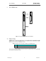
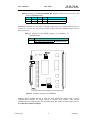
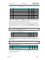
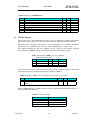
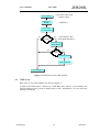
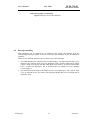
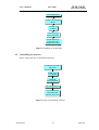
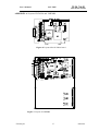
PCI-VME
PCI to VME Interface
User’s Manual
00423.A0
Table of contents:
1.
PCI-VME INTERFACE: GENERAL DESCRIPTION ............................................................................... 1
2.
PCI INTERFACE CARD PCIADA ............................................................................................................... 2
2.1.
2.2.
2.3.
3.
OPERATION ................................................................................................................................................ 2
MAJOR LCREGISTERS ................................................................................................................................ 2
TIMEOUT .................................................................................................................................................... 4
THE VMEMM BOARD.................................................................................................................................. 5
JUMPER SETTINGS ...................................................................................................................................... 5
OPERATION ................................................................................................................................................ 7
VMEMM AREA ......................................................................................................................................... 7
VMEMM CONTROL AND STATUS REGISTERS ........................................................................................... 8
VIC68A-REGISTER .................................................................................................................................. 10
INTERRUPTS ............................................................................................................................................. 11
3.1.
3.2.
3.3.
3.4.
3.5.
3.6.
4.
OPERATING THE INTERFACE ............................................................................................................... 13
INSTALLATION ......................................................................................................................................... 13
INITIALIZING THE INTERFACE ................................................................................................................... 13
VME ACCESS........................................................................................................................................... 14
INTERRUPT HANDLING ............................................................................................................................. 15
UNINSTALLING THE INTERFACE ............................................................................................................... 16
4.1.
4.2.
4.3.
4.4.
4.5.
APPENDIX A : LAYOUT OF PCIADA AND VMEMM...................................................................................... 17
APPENDIX B : POWER REQUIREMENTS OF PCIADA: .................................................................................. 18
APPENDIX C : ACCESS TIMES .......................................................................................................................... 18
List of figures:
FIGURE 1: FRONT PANEL OF VMEMM6 AND VMEMM3............................................................................................ 5
FIGURE 2: LOCATION OF JUMPERS OF VMEMM. ........................................................................................................ 6
FIGURE 3: INITIALIZATION OF THE VME INTERFACE ................................................................................................ 14
FIGURE 4: STEPS TO ACCESS THE VME BUS.............................................................................................................. 15
FIGURE 5: HANDLING OF AN INTERRUPT 1 ................................................................................................................ 16
FIGURE 6: STEPS TO UNINSTALL THE INTERFACE ....................................................................................................... 16
FIGURE 7: LAYOUT OF VMEMM .............................................................................................................................. 17
FIGURE 8: LAYOUT OF THE PCIADA BOARD ............................................................................................................ 17
Legend:
Symbols for jumper settings:
I
=
jumper is installed
:
=
jumper is not installed
February 03
ii
00423.A0
User’s Manual
PCI-VME
W-Ie–Ne-R
Plein & Baus GmbH
1.
PCI-VME Interface: General Description
With the help of the PCI-VME interface which consists of the PCI card PCIADA and the
VME main board VMEMM users of the VME bus profit of the technical success which
takes place in the PC development.
A huge variety of software is available for a PC. In parallel it’s performance was constantly
improved. Modern operating systems were developed which turn the PC into a powerful
workstation.
On the other hand the number of UNIX workstations which are equipped with PCI
increases strongly. The PCI-VME interface can be used in this systems, too.
Drivers and programming tools for PCI-VME are provided for different operating systems
and programming languages.
A driver for Windows offers an easy access to the VME bus. Using pvmon.exe a quick
check of your VME hardware is possible.
For C and Turbo Pascal users the Pascal and c libraries provide easy routines to operate
VME modules.
Using the Linux driver all advantages of a multi user and multi tasking operating system
can be used for VME operations.
VMEMM is available as a 3U (VMEMM-3) and 6U VME module (VMEMM-6). It is
linked via a standard SCSI 2 cable to the PCIADA card. Address modes A16, A24, A32 /
D8, D16, D32 (A16, A24 / D8, D16 for VMEMM-3) are possible.
PCIADA supports 8, 16 and 32 – bit PCI bus slave access. It provides programmable
interrupt generation on PC.
February 03
1
00423.A0
User’s Manual
W-Ie–Ne-R
PCI-VME
Plein & Baus GmbH
2.
PCI interface card PCIADA
2.1. Operation
The major part of the PCIADA card represents the interface chip PCI9050 by PLXTechnology. It manages PCI bus communications.
At booting time necessary setting are configured by PCI auto setup. No jumpers have to be
set on the interface card. All PCIADA information such as memory and IRQ requirements
are stored in an EEPROM called the PCI Configuration Register (PCR). Some IDs can be
read out from PCR:
Table 1: Basic values of the PCI Configuration Register (PCR).
ID
fixed values
Vendor ID
0x10B5
Device ID
0x9050
Subsystem Vendor ID
0x9050
Subsystem Device ID
0x1167
During PCI setup PCIADA calls for three different memory areas:
1. 54 Byte Local Configuration Register (LCR) of the I/O area. Different control status
register and base addresses are available in the LCR. Note: If no LCR is available in the
I/O area please refer to the LCR in the memory area.
2. LCR in the memory area.
3. 8 kByte of the memory area for direct access to VME and the local VMEMM memory
area.
2.2. Major LCRegisters
Base Addresses for the memory areas described in section 2.1 will be available after
booting of the computer. They can be obtained via BIOS from the PLX chip. Most
important are:
The Interrupt Control / Status Register (INTCSR) handles interrupts of the VIC68A
chip (installed on VMEMM), interrupts of PCIADA itself, PCI interrupts and software
interrupts. Sources for the VIC68 A interrupt which are summarized in the INTERRUPT 1
bits are:
1. seven interrupt requests of the VME bus
2. Mailbox interrupts in the VIC068A chip by a second VME-Master
3. interrupts caused by a successful interrupt generation
4. interrupts caused by SYSFAIL or ACFAIL
5. bus timeout interrupt
6. arbitration timeout interrupt
7. VIC68A timer interrupts
8. interrupt caused by a manual reset
February 03
2
00423.A0
User’s Manual
W-Ie–Ne-R
PCI-VME
Plein & Baus GmbH
The INTERUPT2 bits controls local events of the PCIADA card. Interrupts are caused by
1. Timeout while accessing the VME bus. Timeout is fixed to about 35 µs.
2. Cable is not connected.
3. The VME power supply is not switched on.
4. VMEMM access has not yet been switch on. Before any access to VMEMM user bit
I/O 2 has to be set.
Table 1 describes all bits of the INTCSR.
Table 2: Contents of the Interrupt Control / Status Register (INTCSR). Base
address: LCR base address + 0x4c
Bit
RD
WR
after Init
0
yes
yes
1
yes
yes
0
yes
no
0
yes
yes
1
yes
yes
0
yes
no
0
yes
yes
0
yes
yes
yes
no
0
00000000 b
Local Interrupt 1 enable / 1 = enable / 0
= disable / source = VMEMM
1
Local Interrupt 1 polarity / 1 = active high / 0
= active low
2
Local Interrupt 1 status / 1 = active. 0
= not active
3
Local Interrupt 2 enable / 1 = enable / 0 =
disable / Source = PCIADA
4
Local Interrupt 2 polarity / 1 = active high / 0
= active low
5
Local Interrupt 2 status / 1 = active. 0 =
not active
6
PCI Interrupt enable / 1 = enable / 0 =
disable (Source = global)
7
Software Interrupt / 1 = generate Interrupt
16..8 not used
The User I / O Register (CNTRL) is divided into three parts which are summarized in
Table 3. Part one (USER I/O1) must not be modified. The register USER I/O2
1. locks VMEMM during boot time. to prevent any access of the Operating System.
2. resets Interrupt 2 if it is deleted.
Register USER I/O3 monitors the status of the VME crate (on / off) and the cable
(connected / not connected).
Table 3: The User I / O Register (CNTRL). LCR base address + 0x50. To enable access to
VMEMM write 0x4184 into CNTRL, 0x4084 to disable.
Byte
5..0
6
7
8
9
10
11
15..12
February 03
do not modify !
USER I/O2 Type, must always be 0
USER I/O2 Direction, must always be 1 = output
USER I/O2 output, 0 = disable access to VMEMM, 1 = enable
access
USER I/O3 Type, must always be 0
USER I/O3 Direction, must always be 0 = input
USER I/O3 Input, 0 = VMEMM failed , 1 = VMEMM OK
do not modify
3
RD
yes
yes
yes
yes
WR
yes
yes
yes
yes
after Init
000100 b
0
1
0
yes
yes
yes
yes
yes
yes
no
yes
0
0
0
0100 b
00423.A0
User’s Manual
PCI-VME
W-Ie–Ne-R
Plein & Baus GmbH
2.3. Timeout
An Access Timeout is implemented in the PCIADA interface, which is currently set to
about 35 µs. If the VMEMM is switched of or disconnected during an access timeout
causes an Interrupt 2.
February 03
4
00423.A0
User’s Manual
W-Ie–Ne-R
PCI-VME
Plein & Baus GmbH
3.
The VMEMM board
Figure 1: front panel of VMEMM6 and VMEMM3
3.1. Jumper Settings
VMEMM can be operated as a VME master or slave module which is controlled by the SC
jumper (Table 4). Insert VMEMM into slot 1 if it should work as VME Master. Jumper
position can be read out by VMEMM-STATUS.
Table 4: Settings of the SC jumper (readable by VMEMM-Status)
J402
I
:
Function
VMEMM works as System Controller (default)
VMEMM works as Slave
Choose different Board Numbers which are selected via jumper J304 to J301 if more than
one PCIADA is installed in one PC.
February 03
5
00423.A0
User’s Manual
PCI-VME
W-Ie–Ne-R
Plein & Baus GmbH
Table 5: Settings of the Board Number BN Jumpers, which can be read out by the
register VMEMM-Status
J304
BN3
I
J303
BN2
I
J302
BN1
I
J301
BN0
:
Function
Bits of BN (BN0: Low Bit)
Default value BN = 1
VMEMM is available as a 6U and a 3U board. Long word access is not possible for the 3U
version (J1 / P1 does not exist). The VIC068 A chip checks the WORD Jumper before a
long word access.
Table 6: Settings of the WORD jumper. It is readable via
VMEMM-Status.
J401
I
:
Function
VIC-Chip in word mode
(VMEMM3 default)
VIC-Chip in long word-mode (VMEMM6 default)
Figure 2: Location of jumpers of VMEMM.
VMEbus allows multiple masters to share the data transfer bus which needs a special
communication between all master boards to organize data transfer. Inter process
communication are important for this communication. The address of this register is set by
the VME Short Address Jumper.
February 03
6
00423.A0
User’s Manual
W-Ie–Ne-R
PCI-VME
Plein & Baus GmbH
Note:
Watch the setting of the VME Short Address. The address range can not be
masked. An access by VMEMM itself will cause a _BERR* and will not be
ended by _DTACK.
Table 7: VME Short Address Jumper. Note: An inserted jumper means bit = 0.
J608
A15
:
J607
A14
I
J606
A13
:
J605
A12
I
J604
A11
:
J603
A10
I
J602
A9
:
J601 Function
A8
VME Short Address
I
VME Short = 0xAA00
(default)
3.2. Operation
PCIADA accesses a region of the VMEMM memory directly. This region is divided into
four blocks:
1. VMEMM: VME addresses A11 to A31 and control signal RMC are stored here and
VME reset is activated. Signals VMEMM-Stat, IRQ Status and A11 to A31 are
readable.
2. VIC068A: This is the part of the VMEbus Interface Controller which controls the
VMEbus.
3. Interrupt Vector (INTVEC): An interrupt acknowledge cycle is stated if one byte of
this area is accessed.
4. VME: Every time this area is accessed a VMEbus transfer will be started. Address
lines A11 to A1 equals PCI address lines A11 to A1. VME address lines A31 to A12
are stored in the VMEADR register.
Following sections describe each memory block in details.
3.3. VMEMM area
The size of this block is 8 kByte and it is mapped into the PCI memory. The PCI base
address is defined by the BIOS during boot time.
February 03
7
00423.A0
User’s Manual
W-Ie–Ne-R
PCI-VME
Plein & Baus GmbH
Table 8: Contents of the VMEMM which is mapped into the PCI memory area.
Base-Address
+ $1FFF
to
+ $1000
VMEBASE
+ $080F
+ $080D
+ $080A
+ $0809
+ $0807
+ $0805
+ $0803
VECBASE
+ $04E3
to
+ $0403
VICBASE
(+ $000a)
region / access
WR-function
VME
VME
VME
VME
D07..D00
D07..D00
D15..D00
D31..D00
(+ $0008)
VMEMM / word
+ $0008
VMEMM / lword
+ $0004
VMEMM / word
+ $0000
VMEMM / word
/
/
/
/
byte A0 = 0
byte A0 = 1
word
lword
RD-function
D15..D00
D07..D00
D15..D00
D31..D00
<
<
<
<
VME-D15..D08
VME-D07..D00
VME-D15..D00
VME-D31..D00
-
D07..D00
D07..D00
D07..D00
D07..D00
D07..D00
D07..D00
D07..D00
<
<
<
<
<
<
<
Iack
Iack
Iack
Iack
Iack
Iack
Iack
VIC / byte
VIC / byte
VIC / byte
VIC068A Reg.
VIC068A Reg.
VIC068A Reg.
VIC068A Reg.
VIC068A Reg.
VIC068A Reg.
VMEMM / word
VMEADRReg high
D15..D00 > VME-A31..A16
VMEADRReg low
D15..D12 > VME-A15..A12
D11..D00 > x
VMEADRReg
D31..D12 > VME-A31..A12
D11..D00 > x
VMEVICReset
D15..D00 > h000a
1*
D15..D00 > h0005
2*
VMEADRStat high
D15..D00 = VME-A31..A16
VMEADRStat low
D15..D12 = VME-A15..A12
D11..D00 = 0
VMEADRStat
D31..D12 = VME-A31..A12
D11..D00 = 0
VMEMMIRQStat
D0 = IRQ > 1= aktiv
D1 = IPL0
D2 = IPL1
D3 = IPL2
D15..D04 = 0
VMEMMStat
D0 < RMC-VIC068A
3*
D1 = BLT-VIC068A
4*
D2 < WORD Jumper sel.
D3 < SC
Jumper sel.
D07..D04 = Modul-Number
D11..D08 = FPGA-Revision
D15..D12 = module-Type
INTVEC /
INTVEC /
INTVEC /
INTVEC /
INTVEC /
INTVEC /
INTVEC/
byte
byte
byte
byte
byte
byte
byte
>
>
>
>
VME-D15..D08
VME-D07..D00
VME-D15..D00
VME-D31..D00
VMEVICReg
D0 > RMC-VIC048A
7
6
5
4
3
2
1
Vector
Vector
Vector
Vector
Vector
Vector
Vector
PCI-MEMBASE
1*
2*
3*
4*
VIC „Global Reset“ ( refer to VIC068A Manual )
VIC „Internal Reset“ ( refer to VIC068A Manual )
Read Modify Cycle (refer to VIC068A Manual )
Blocktransfer = fix disabled
3.4. VMEMM Control and Status registers
You find important information about configuration and controlling of the interface in the
VMEMM Control and Status registers.
Register VMEADDR contains high bytes of VMEbus addresses (A31 to A12) of the
following accesses. Data bit D11 to D0 are ignored during write and replied as ‘0’ during
read.
Note:
Addresses A31 to A24 (A31 to A16) have no meaning for standard (short I/O)
VMEbus accesses.
Note:
VMEADDR is read- and writeable in word or long word mode.
February 03
8
00423.A0
User’s Manual
W-Ie–Ne-R
PCI-VME
Plein & Baus GmbH
Table 9: Contents of the VMEADDR register for word or long word read- write
access.
Bit
31..12
11..0
Bit
31..24
23..12
11..0
Bit
31..16
15..12
11..0
extended
most significant address bit A31 .. A12
write: no meaning, read returns 0
Standard
no meaning
most significant address bit A23 .. A12
write: no meaning, read returns 0
Short
no meaning
most significant address bit A15 .. A12
write: don’t care, read returns 0
RD
yes
yes
RD
yes
yes
yes
RD
yes
yes
yes
WR
yes
yes
WR
yes
yes
yes
WR
yes
yes
yes
after Init
X
0
after Init
X
X
0
after Init
X
X
0
Reset functions are handled by the VMEReset register. Write data word 0x000a into
VMER to perform a VMEbus reset and a global reset of the interface which equals a power
up reset. After this a reinitialization of VMEMM is mandatory.
Pushing the reset button on the front panel will cause an interrupt. Further actions have to
be preformed by software. This method allows an individual programming of the button.
Interrupt information of the VIC068A chip are stored in the VMEMMIRQ status register.
An interrupt request sets D0 to ‘1’. The request which has highest priority is encoded in D3
to D1.
Note:
The index of the corresponding interrupt vector can be calculated very fast since
no shift of VMEMMIRQ shift is necessary.
Table 10: Register VMEMMIRQStatus.
bit
15..4
3..1
0
0
interrupt level
0 = no interrupt pending, 1 = interrupt pending
RD
yes
yes
yes
WR
no
no
no
after Init
0
0
0
The VMEVICRegister used to realize unresetable cycles. If RMC (= D0) is set signal _AS
(Address Strobe) will remain active for all following VMEbus accesses. Bits D15 to D1
must be set to ‘0’.
Note:
VMEbus allows only single address unresetable cycles. The address must not be
changed during the unresetable cycle.
Table 11: Register VMEVIC.
Bit
15..1
0
must be 0
RMC, 0 = No Read-Modify-Write-Cycle,
1 = Read-Modify-Write-Cycle
RD
no
no
WR
yes
yes
after Init
X
0
Various settings of VMEMM are stored in register VMEMMStatus. Refer to section 3.1
for WORD and Module Number
February 03
9
00423.A0
User’s Manual
W-Ie–Ne-R
PCI-VME
Plein & Baus GmbH
Table 12: Register VMEMMStatus.
Bit
15..12
11..8
7..4
3
2
1
0
RD
yes
yes
yes
yes
yes
yes
yes
module type Identification, 0001b for VMEMM-Modul
FPGA-Revision
module number, coding of Jumpers J304..J301
SC – status of system controller Jumper J402
WORD – status of word-path jumper J401
BLT (fix 0)
RMC (status of VMEVICReg RMC)
WR
no
no
no
no
no
no
no
after Init
0001b
xxxx
Jumpers
Jumpers
Jumpers
0
0
3.5. VIC68A-Register
This section gives a short description of some VIC68 A registers. For further information
please refer to the Cypress VIC068 A data sheet which is distributed with this interface.
Registers can be accessed in byte mode. A 4 byte offset has to be considered for address
calculations (e. g. VMEMM_base + 0x403 + 0x0, VMEMM_base + 0x403 + 0x4, ...).
The Address Modifier for the next VMEbus access is stored in the Address Modifier
Source Register (AMSR). It does not influence Interrupt Acknowledge Cycles.
Table 13: Register AMSR. VIC base address +
0xB7 (byte access only).
Bit
7
6
5..0
must be 0
must be 0
AM5 .. AM0
RD
yes
yes
yes
WR
yes
yes
yes
after Init
0
0
00000
The VIC chip generates a SYSFAIL after each reset of the VMEbus which is deactivated
by the Interprocessor Communication Register number 7 (ICR7).
Table 14: Register ICR7. VIC-base address + 0x7F (byte-access only).
Bit
7
6..0
SYSFAIL-MASK, 1 deaktiviert SYSFAIL
further functions are described in the VIC68 A
manual
RD
yes
yes
WR
yes
yes
after Init
0
00x0000
Register TTR handles the VMEbus timeout. Values smaller than the PCIADA timeout e. g.
4 or 16 µs should be inserted.
Table 15: Timeout coding.
Timeout / µs
4
16
32
switched off (infinite)
February 03
Bit-Code (Bits 7..5 or 4..2)
0
1
2
7
10
00423.A0
User’s Manual
W-Ie–Ne-R
PCI-VME
Plein & Baus GmbH
Table 16: Register TTR. VIC base address + 0xA3 (byte access only)
Bit
7..5
4..2
1
0
VME-BUS Timeout Period (see table below)
Local BUS Timeout Period (see table below)
Arbitration Timeout detected; 1 = detected
With VME-BUS Aquisition Time included
RD
yes
yes
yes
yes
WR
yes
yes
no
yes
after Init
32 usec
32 usec
not incl.
Events VMEbus timeout (local interrupt number 7) and “front panel buttom pushed” (local
interrupt number 6) are processed via local interrupts. Timeout causes an interrupt number
7 and the bottom causes interrupt 6. For this reason it is necessary to setup registers LICRx
(Local Interrupt Control Register) and LIVBR (Local Interrupt Vector Base Register). The
upper 5 bits of the interrupt vector are stored in LEIVBR. Lower bits codes the source layer
of the causing interrupt. Please refer to section 3.6 for further information.
Table 17: Register LICR. VIC base address 0x3B / 0x3F (byte access only).
Bits
7
6
5
4
3
2..0
Interrupt Mask; 0 = clear, 1 = masked off
Polarity of input; 1 = high or rising edge; use always a falling edge
Edge or level sensitive input; 1 = edge sensitive input; use always edge
Autovector enable; Must be 1; LIVBR supplies vector
Interrupt status; 0 = interrupt is asserted
Interrupt level to map; always map to the same level as the input
RD
WR
yes
yes
yes
yes
yes
yes
yes
yes
yes
yes
no
yes
after
Init
1
3.6. Interrupts
VMEbuss accesses causing a VMEbus timeout or a BERR* signal are treated as a normal
access by VMEMM. But they result in a local interrupt number 7 which has to be checked
by software.
Pushing the front panel button causes only a local interrupt number 6. All specific reset
functions have to be defined in the software.
The falling flank of input LIRQ7 (LICR6) has to be considered to calculate the exact
timeout.
It is mandatory to convert internal interrupts into vectors before any other action is
performed. Usually internal events which are caused by drivers generate vectors between
0x00 to 0x0F. Other VME boards use Vector addresses from 0x40 to 0xff.
Note:
Local interrupts expect VMEMM to generate the interrupt vector.
Note:
The PCIADA timeout interrupt has to be mirrored in interrupt vector number 1.
February 03
11
00423.A0
User’s Manual
PCI-VME
W-Ie–Ne-R
Plein & Baus GmbH
Table 18: Coding of interrupt signals.
Interrupt source
Interrupt caused by PCIADA (timeout)
Clock tick interrupt generator
Reset button at front panel
VMEbus Timeout (Bus-Error)
Interprocess communication global switch #0
Interprocess communication global switch #1
Interprocess communication global switch #2
Interprocess communication global switch #3
Interprocess communication module switch #0
Interprocess communication module switch #1
Interprocess communication module switch #2
Interprocess communication module switch #3
ACFAIL asserted
Write post Fail
Arbitration Timeout
SYSFAIL asserted
VMEbus Interrupter acknowledge
February 03
12
vector no.
1
2
6
7
8
9
10
11
12
13
14
15
16
17
18
19
20
00423.A0
User’s Manual
PCI-VME
W-Ie–Ne-R
Plein & Baus GmbH
4.
Operating the Interface
4.1. Installation
Note:
To protect interface and your computer against damage from static electricity
follow some major precautions:
1. Before unpacking the interface be sure that your working area is discharged.
2. Switch of and unplug computer and VME crate.
3. Be sure that VME crate and Computer are on the same electrical potential.
For the installation procedure stay close to the following procedure:
1. Check all jumper settings. Refer to section 3.1 for VMEMM. There are no jumpers on
PCIADA.
2. Insert PCIADA into your Computer and fix it by a screw.
3. Insert VMEMM into your VME Crate and tight the screws.
4. Connect the interface cable to PCIADA and VMEMM.
5. To install the PCI-VME WIN95 driver follow instructions of the manual.
6. Windows95 will recognize PCIADA as new hardware and will ask for a driver.
Activate “do not install a driver” and press “o.k.”.
7. If you use Pascal drivers you have to edit the emm386.exe in config.sys. You will find
details in a:\dos\pascal\readme.txt.
8. Check your interface using the supplied test programs.
4.2. Initializing the interface
Necessary steps to initialize the interface are summarized in Figure 3.
For further information please refer to the supplied code written in Turbo Pascal (DOS) and
C++ (Windows 95).
February 03
13
00423.A0
User’s Manual
W-Ie–Ne-R
PCI-VME
Plein & Baus GmbH
get PCI address
e.g. from bios calls or from
windows registry
enable access
in LCR
USER I/O = 1
test user I/O 3+
try a VME access
no
Access
successful ?
yes
access interface. After
40 µs poll for Interrupt 2
get module type
and module ID
no
correct
interface ?
yes
initialize VIC68A
remove SYSFAIL
end of initialization
Figure 3: Initialization of the VME interface
4.3. VME access
Basic steps to access the VMEbus are shown in Figure 4
A VME access which causes a Timeout or a VME BUS Error ends it’s cycle normally. The
Timeout Interrupt can be used to identify these events. Alternatively, you can check the
Interrupt 1 Status Bit.
February 03
14
00423.A0
User’s Manual
PCI-VME
W-Ie–Ne-R
Plein & Baus GmbH
Fehler! Keine gültige Verknüpfung.
Figure 4: Steps to access the VME bus.
4.4. Interrupt handling
VME Interrupts can be handled in two different ways. Either the software polls the
corresponding interrupt register or they are converted into interrupts for the PCIADA host
computer.
There are two different interrupt sources which cause a PCI interrupt:
1. All VME Interrupts are summarized in Local Interrupt 1. Interrupt Priorities have to be
defined in the VIC68A chip except for Interrupts with a certain VME priority which
require a high local priority and the VME BUS Error which is fixed to local interrupt
level 7. Each Local Interrupt 1 has to be followed by a readout of a byte interrupt
vector (Figure 5).
2. The local Timeout Interrupt on PCIADA causes a Local Interrupt 2. The value is fixed
on 35 µs after the access was started. The interrupt finishes the access resulting into an
indefinite value.
February 03
15
00423.A0
User’s Manual
PCI-VME
W-Ie–Ne-R
Plein & Baus GmbH
read VMEIRQStatus
calculate corresponding
address
read byte out
of address
remove interrupt
source if necessary
set end of interrupt
at local interrupt
controller if necessary
Figure 5: Handling of an Interrupt 1
4.5. Uninstalling the interface
Figure 6 describes how to uninstall the interface.
set SYSFAIL in VIC68 A
if necessary
disable access
to VMEMM
disable all
Interrupt Enable
end of deinitialization
set end of interrupt
at local interrupt
controller if necessary
Figure 6: Steps to uninstall the interface
February 03
16
00423.A0
User’s Manual
PCI-VME
W-Ie–Ne-R
Plein & Baus GmbH
APPENDIX A: Layout of PCIADA and VMEMM
Figure 8: Layout of the PCIADA board
Figure 7: Layout of VMEMM
February 03
17
00423.A0
User’s Manual
W-Ie–Ne-R
PCI-VME
Plein & Baus GmbH
APPENDIX B: Power requirements of PCIADA:
Voltage:
+ 5V
Current:
≈ 0.5 A
Power:
≈ 2.5 W
APPENDIX C: Access times
Access
WR-time / ns
RD-time / ns
PCI to VMEMM VIC. Reg. D8
PCI to VMEMM Adr. Reg. D16
PCI to VMEMM Adr. Reg. D32
( DS to DTACK ca. 20 ns)
PCI to VME-D8
( DS to DTACK ca. 20 ns)
PCI to VME-D16
( DS to DTACK ca. 20 ns)
PCI to VME-D32
600
450
500
660
660
750
1000
950
1300
1200
1200
1500
February 03
18
00423.A0