1
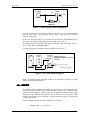
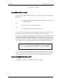
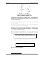
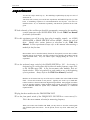
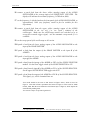
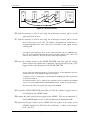
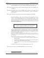
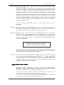
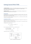
MODELLING EQUATIONS
modules
basic: ADDER, AUDIO OSCILLATOR, PHASE SHIFTER
optional basic: MULTIPLIER
preparation
This experiment assumes no prior knowledge of telecommunications. It illustrates how
TIMS is used to model a mathematical equation. You will learn some experimental
techniques. It will serve to introduce you to the TIMS system, and prepare you for the more
serious experiments to follow.
In this experiment you will model a simple trigonometrical equation. That is, you will
demonstrate in hardware something with which you are already familiar analytically.
This is not a typical TIMS Lab Sheet. It gives much more detail than later sheets.
an equation to model
You will see that what you are to do experimentally is to demonstrate that two AC signals of
the same frequency, equal amplitude and opposite phase, when added, will sum to zero.
This process is used frequently in communication electronics as a means of removing, or at
least minimizing, unwanted components in a system. You will meet it in later experiments.
The equation which you are going to model is:
y(t) = V1 sin(2πf1t) + V2 sin(2πf2t + α)
= v1(t) + v2(t)
........ 1
........ 2
Here y(t) is described as the sum of two sine waves. Every young trigonometrician knows
that, if:
........ 3
each is of the same frequency:
f1 = f2 Hz
........ 4
each is of the same amplitude:
V1 = V2 volts
and they are 180o out of phase:
then:
α = 180 degrees
y(t) = 0
........ 5
........ 6
A block diagram to represent eqn.(1) is suggested in Figure 1.
Copyright © 2005 Emona Instruments Pty Ltd
1/10
Emona-TIMS
modelling equations L-02 rev 1.4
SOURCE
ADDER
v1 (t)
OUT
y(t)
V sin2 πf1t
-1
INVERTING
AMPLIFIER
v (t)
2
Figure 1: block diagram model of Equation 1
Note that we ensure the two signals are of the same frequency (f1 = f2) by obtaining them
from the same source. The 180 degree phase change is achieved with an inverting
amplifier, of unity gain.
In the block diagram of Figure 1 it is assumed, by convention, that the ADDER has unity
gain between each input and the output. Thus the output is y(t) of eqn.(2).
This diagram appears to satisfy the requirements for obtaining a null at the output. Now see
how we could model it with TIMS modules.
A suitable arrangement is illustrated in block diagram form in Figure 2.
OSCILLOSCOPE and
FREQUENCY COUNTER connections
not shown.
v (t)
2
y(t) = g.v1(t) + G.v2(t)
v (t)
= V sin2π f1t + V2 sin2πf2t
1
1
Figure 2: the TIMS model of Figure 1.
Before you build this model with TIMS modules let us consider the procedure you might
follow in performing the experiment.
the ADDER
The annotation for the ADDER needs explanation. The symbol ‘G’ near input A means the
signal at this input will appear at the output, amplified by a factor ‘G’. Similar remarks
apply to the input labelled ‘g’. Both ‘G’ and ‘g’ are adjustable by adjacent controls on the
front panel of the ADDER. But note that, like the controls on all of the other TIMS
modules, these controls are not calibrated. You must adjust these gains for a desired final
result by measurement.
Thus the ADDER output is not identical with eqn.(2), but instead:
ADDER output = g.v1(t) + G.v2(t)
TIMS Lab Sheet
Copyright © 2005 Emona Instruments Pty Ltd
........ 7
2/10
Emona-TIMS
modelling equations L-02 rev 1.4
= V1 sin2πf1t + V2 sin2πf2t
........ 8
conditions for a null
For a null at the output, sometimes referred to as a ‘balance’, one would be excused for
thinking that:
if:
1) the PHASE SHIFTER is adjusted to introduce a difference of 180o between
its input and output
and
2) the gains ‘g’ and ‘G’ are adjusted to equality
then
3) the amplitude of the output signal y(t) will be zero.
In practice the above procedure will almost certainly not result in zero output ! Here is the
first important observation about the practical modelling of a theoretical concept.
In a practical system there are inevitably small impairments to be accounted for. For
example, the gain through the PHASE SHIFTER is approximately unity, not exactly so. It
would thus be pointless to set the gains ‘g’ and ‘G’ to be precisely equal. Likewise it would
be a waste of time to use an expensive phase meter to set the PHASE SHIFTER to exactly
180o, since there are always small phase shifts not accounted for elsewhere in the model.
These small impairments are unknown, but they are stable.
Once compensated for they produce no further problems.
So we do not make precise adjustments to modules, independently of the system into which
they will be incorporated, and then patch them together and expect the system to behave.
All adjustments are made to the system as a whole to bring about the desired end result.
more insight into the null
It is instructive to express eqn. (1) in phasor form. Refer to Figure 3.
TIMS Lab Sheet
Copyright © 2005 Emona Instruments Pty Ltd
3/10
Emona-TIMS
modelling equations L-02 rev 1.4
Figure 3: Equation (1) in phasor form
The null at the output of the simple system of Figure 2 is achieved by adjusting the
uncalibrated controls of the ADDER and of the PHASE SHIFTER. Although equations (3),
(4), and (5) define the necessary conditions for a null, they do not give any guidance as to
how to achieve these conditions.
Figure 3 (a) and (b) shows the phasors V1 and V2 at two different angles α. It is clear that,
to minimise the length of the resultant phasor (V1 + V2), the angle α in (b) needs to be
increased by about 45o.
The resultant having reached a minimum, then V2 must be increased to approach the
magnitude of V1 for an even smaller (finally zero) resultant.
We knew that already. What is clarified is the condition prior to the null being achieved.
Note that, as angle α is rotated through a full 360o, the resultant (V1 + V2) goes through one
minimum and one maximum (refer to the TIMS User Manual to see what sort of phase
range is available from the PHASE SHIFTER).
What is also clear from the phasor diagram is that, when V1 and V2 differ by more than
about 2:1 in magnitude, the minimum will be shallow, and the maximum broad and not
pronounced 1.
Thus we can conclude that, unless the magnitudes V1 and
V2 are already reasonably close, it may be difficult to find
the null by rotating the phase control.
So, as a first step towards finding the null, it would be wise to set V2 close to V1. This will
be done in the procedures detailed below.
Note that, for balance, it is the ratio of the magnitudes V1 and V2 , rather than their absolute
magnitudes, which is of importance.
So we will consider V1 of fixed magnitude (the
reference), and make all adjustments to V2.
This assumes V1 is not of zero amplitude !
TIMS Lab Sheet
1 fix V as reference; mentally rotate the phasor for V . The dashed circle shows the locus of its extremity.
1
2
Copyright © 2005 Emona Instruments Pty Ltd
4/10
Emona-TIMS
modelling equations L-02 rev 1.4
experiment
You are now ready to model eqn. (1). The modelling is explained step-by-step as a series of
small tasks T.
Take these tasks seriously, now and in later experiments, and TIMS will provide you with
hours of stimulating experiences in telecommunications and beyond. The tasks are
identified with a ‘T’, are numbered sequentially, and should be performed in the order
given.
T1 both channels of the oscilloscope should be permanently connected to the matching
coaxial connectors on the SCOPE SELECTOR. See the TIMS User Manual
for details of this module.
T2 in this experiment you will be using three plug-in modules, namely: an AUDIO
OSCILLATOR, a PHASE SHIFTER, and an ADDER. Obtain one each of
these. Identify their various features as described in the TIMS User
Manual. In later experiments always refer to this manual when meeting a
module for the first time.
Most modules can be controlled entirely from their front panels, but some have switches
mounted on their circuit boards. Set these switches before plugging the modules into the
TIMS SYSTEM UNIT; they will seldom require changing during the course of an
experiment.
T3 set the on-board range switch of the PHASE SHIFTER to ‘LO’. Its circuitry is
designed to give a wide phase shift in either the audio frequency range (LO),
or the 100 kHz range (HI). A few, but not many other modules, have onboard switches. These are generally set, and remain so set, at the beginning
of an experiment. Always refer to the TIMS User Manual if in doubt.
Modules can be inserted into any one of the twelve available slots in the TIMS SYSTEM
UNIT. Choose their locations to suit yourself. Typically one would try to match their
relative locations as shown in the block diagram being modelled. Once plugged in, modules
are in an operating condition. When modelling large systems extra space can be obtained
with an additional TIMS-301 System Unit, a TIMS-801 TIMS-Junior, or a TIMS-240
Expansion Rack.
T4 plug the three modules into the TIMS SYSTEM UNIT.
T5 set the front panel switch of the FREQUENCY COUNTER to a GATE
This is the most common selection for measuring frequency.
TIME
of 1s.
When you become more familiar with TIMS you may choose to associate certain signals
with particular patch lead colours. For the present, choose any colour which takes your
fancy.
TIMS Lab Sheet
Copyright © 2005 Emona Instruments Pty Ltd
5/10
Emona-TIMS
modelling equations L-02 rev 1.4
T6 connect a patch lead from the lower yellow (analog) output of the AUDIO
OSCILLATOR to the ANALOG input of the FREQUENCY COUNTER. The
display will indicate the oscillator frequency f1 in kilohertz (kHz).
T7 set the frequency f1 with the knob on the front panel of the AUDIO OSCILLATOR, to
approximately 1 kHz (any frequency would in fact be suitable for this
experiment).
T8 connect a patch lead from the upper yellow (analog) output of the AUDIO
OSCILLATOR to the ‘ext. trig’ [ or ‘ext. synch’ ] terminal of the
oscilloscope. Make sure the oscilloscope controls are switched so as to
accept this external trigger signal; use the automatic sweep mode if it is
available.
T9 set the sweep speed of the oscilloscope to 0.5 ms/cm.
T10 patch a lead from the lower analog output of the AUDIO OSCILLATOR to the
input of the PHASE SHIFTER.
T11 patch a lead from the output of the PHASE SHIFTER to the input G of the
ADDER 2.
T12 patch a lead from the lower analog output of the AUDIO OSCILLATOR to the
input g of the ADDER.
T13 patch a lead from the input g of the ADDER to CH2-A of the SCOPE SELECTOR
module. Set the lower toggle switch of the SCOPE SELECTOR to UP.
T14 patch a lead from the input G of the ADDER to CH1-A of the SCOPE SELECTOR.
Set the upper SCOPE SELECTOR toggle switch UP.
T15 patch a lead from the output of the ADDER to CH1-B of the SCOPE SELECTOR.
This signal, y(t), will be examined later on.
Your model should be the same as that shown in Figure 4 below, which is based on
Figure 2. Note that in future experiments the format of Figure 2 will be used for TIMS
models, rather than the more illustrative and informal style of Figure 4, which depicts the
actual flexible patching leads.
You are now ready to set up some signal levels.
TIMS Lab Sheet
2 the input is labelled ‘A’, and the gain is ‘G’. This is often called ‘the input G’; likewise ‘input g’.
Copyright © 2005 Emona Instruments Pty Ltd
6/10
Emona-TIMS
modelling equations L-02 rev 1.4
v2(t)
v (t)
1
Figure 4: the TIMS model.
T16 find the sinewave on CH1-A and, using the oscilloscope controls, place it in the
upper half of the screen.
T17 find the sinewave on CH2-A and, using the oscilloscope controls, place it in the
lower half of the screen. This will display, throughout the experiment, a
constant amplitude sine wave, and act as a monitor on the signal you are
working with.
Two signals will be displayed. These are the signals connected to the two ADDER inputs.
One goes via the PHASE SHIFTER, which has a gain whose nominal value is unity; the
other is a direct connection. They will be of the same nominal amplitude.
T18 vary the COARSE control of the PHASE SHIFTER, and show that the relative
phases of these two signals may be adjusted. Observe the effect of the ±1800
toggle switch on the front panel of the PHASE SHIFTER.
As part of the plan outlined previously it is now necessary to set the amplitudes of the two
signals at the output of the ADDER to approximate equality.
Comparison of eqn. (1) with Figure 2 will show that the ADDER gain control g will adjust
V1, and G will adjust V2.
You should set both V1 and V2, which are the magnitudes of the two signals at the ADDER
output, at or near the TIMS ANALOG REFERENCE LEVEL, namely 4 volt peak-to-peak.
Now let us look at these two signals at the output of the ADDER.
T19 switch the SCOPE SELECTOR from CH1-A to CH1-B. Channel 1 (upper trace) is
now displaying the ADDER output.
T20 remove the patch cords from the g input of the ADDER. This sets the amplitude V1
at the ADDER output to zero; it will not influence the adjustment of G.
T21 adjust the G gain control of the ADDER until the signal at the output of the
ADDER, displayed on CH1-B of the oscilloscope, is about 4 volt peak-topeak. This is V2.
TIMS Lab Sheet
Copyright © 2005 Emona Instruments Pty Ltd
7/10
Emona-TIMS
modelling equations L-02 rev 1.4
T22 remove the patch cord from the G input of the ADDER. This sets the V2 output
from the ADDER to zero, and so it will not influence the adjustment of g.
T23 replace the patch cords previously removed from the g input of the ADDER, thus
restoring V1.
T24 adjust the g gain control of the ADDER until the signal at the output of the
ADDER, displayed on CH1-B of the oscilloscope, is about 4 volt peak-topeak. This is V1.
T25 replace the patch cords previously removed from the G input of the ADDER.
Both signals (amplitudes V1 and V2) are now displayed on the upper half of the screen
(CH1-B). Their individual amplitudes have been made approximately equal. Their
algebraic sum may lie anywhere between zero and 8 volt peak-to-peak, depending on the
value of the phase angle α. It is true that 8 volt peak-to-peak would be in excess of the
TIMS ANALOG REFERENCE LEVEL, but it won`t overload the oscilloscope, and in any
case will soon be reduced to a null.
Your task is to adjust the model for a null at the ADDER
output, as displayed on CH1-B of the oscilloscope.
You may be inclined to fiddle, in a haphazard manner, with the few front panel controls
available, and hope that before long a null will be achieved. You may be successful in a few
moments, but this is unlikely. Such an approach is definitely not recommended if you wish
to develop good experimental practices.
Instead, you are advised to remember the plan discussed above. This should lead you
straight to the wanted result with confidence, and the satisfaction that instant and certain
success can give.
There are only three conditions to be met, as defined by equations (3), (4), and (5).
•
•
•
the first of these is already assured, since the two signals are coming from a
common oscillator.
the second is approximately met, since the gains ‘g’ and ‘G’ have been adjusted
to make V1 and V2, at the ADDER output, about equal.
the third is unknown, since the front panel control of the PHASE SHIFTER is not
calibrated 3.
It would thus seem a good idea to start by adjusting the phase angle α. So:
T26 set the FINE control of the PHASE SHIFTER to its central position.
TIMS Lab Sheet
3 TIMS philosophy is not to calibrate any controls. In this case it would not be practical, since the phase range of
the PHASE SHIFTER varies with frequency.
Copyright © 2005 Emona Instruments Pty Ltd
8/10
Emona-TIMS
modelling equations L-02 rev 1.4
T27 whilst watching the upper trace, y(t) on CH1-B, vary the COARSE control of the
PHASE SHIFTER. Unless the system is at the null or maximum already,
rotation in one direction will increase the amplitude, whilst in the other will
reduce it. Continue in the direction which produces a decrease, until a
minimum is reached. That is, when further rotation in the same direction
changes the reduction to an increase. If such a minimum can not be found
before the full travel of the COARSE control is reached, then reverse the front
panel 180O TOGGLE SWITCH, and repeat the procedure. Keep increasing the
sensitivity of the oscilloscope CH1 amplifier, as necessary, to maintain a
convenient display of y(t).
Leave the PHASE SHIFTER controls in the position which gives the
minimum.
T28 now select the G control on the ADDER front panel to vary V2, and rotate it in the
direction which produces a deeper null. Since V1 and V2 have already been
made almost equal, only a small change should be necessary.
T29 repeating the previous two tasks a few times should further improve the depth of
the null. As the null is approached, it will be found easier to use the FINE
control of the PHASE SHIFTER. These adjustments (of amplitude and
phase) are NOT interactive, so you should reach your final result after only
a few such repetitions.
Nulling of the two signals is complete !
You have achieved your first objective
You will note that it is not possible to achieve zero output from the ADDER. This never
happens in a practical system. Although it is possible to reduce y(t) to zero, this cannot be
observed, since it is masked by the inevitable system noise.
T30 reverse the position of the PHASE SHIFTER toggle switch. Record the amplitude
of y(t), which is now the absolute sum of V1 PLUS V2. Set this signal to fill
the upper half of the screen. When the 1800 switch is flipped back to the null
condition, with the oscilloscope gain unchanged, the null signal which
remains will appear to be ‘almost zero’.
signalsignal-toto-noise ratio
When y(t) is reduced in amplitude, by nulling to well below the TIMS ANALOG
REFERENCE LEVEL, and the sensitivity of the oscilloscope is increased, the inevitable
noise becomes visible. Here noise is defined as anything we don`t want.
The noise level will not be influenced by the phase cancellation process which operates on
the test signal, so will remain to mask the moment when y(t) vanishes.
It will be at a level considered to be negligible in the TIMS environment - say less then
10 mV peak-to-peak. How many dB below reference level is this ?
TIMS Lab Sheet
Copyright © 2005 Emona Instruments Pty Ltd
9/10
Emona-TIMS
modelling equations L-02 rev 1.4
Note that the nature of this noise can reveal many things.
achievements
Compared with some of the models you will be examining in later experiments you have
just completed a very simple exercise. Yet many experimental techniques have been
employed, and it is fruitful to consider some of these now, in case they have escaped your
attention.
•
•
•
•
to achieve the desired proportions of two signals V1 and V2 at the output of an
ADDER it is necessary to measure first one signal, then the other. Thus it is
necessary to remove the patch cord from one input whilst adjusting the output
from the other. Turning the unwanted signal off with the front panel gain control
is not a satisfactory method, since the original gain setting would then be lost.
as the amplitude of the signal y(t) was reduced to a small value (relative to the
remaining noise) it remained stationary on the screen. This was because the
oscilloscope was triggering to a signal related in frequency (the same, in this
case) and of constant amplitude, and was not affected by the nulling procedure.
So the triggering circuits of the oscilloscope, once adjusted, remained adjusted.
choice of the oscilloscope trigger signal is important. Since the oscilloscope
remained synchronized, and a copy of y(t) remained on display (CH1) throughout
the procedure, you could distinguish between the signal you were nulling and the
accompanying noise.
remember that the nulling procedure was focussed on the signal at the oscillator
(fundamental) frequency. Depending on the nature of the remaining unwanted
signals (noise) at the null condition, different conclusions can be reached.
a) if the AUDIO OSCILLATOR had a significant amount of harmonic distortion,
then the remaining ‘noise’ would be due to the presence of these harmonic
components. It would be unlikely for them to be simultaneously nulled.
The ‘noise’ would be stationary relative to the wanted signal (on CH1).
The waveform of the ‘noise’ would provide a clue as to the order of the
largest unwanted harmonic component (or components).
b) if the remaining noise is entirely independent of the waveform of the signal
on CH1, then one can make statements about the waveform purity of the
AUDIO OSCILLATOR.
more models
Before entering the realm of telecommunications (with the help of other TIMS Lab Sheets),
there are many equations familiar to you that can be modelled. For example, try
demonstrating the truth of typical trigonometrical identities, such as:
•
•
•
•
•
cosA.cosB = ½ [ cos(A-B) + cos(A+B) ]
sinA.sinB = ½ [ cos(A-B) - cos(A+B) ]
sinA.cosB = ½ [ sin(A-B) + sin(A+B) ]
cos2A = ½ + ½ cos2A
sin2A = ½ - ½ cos2A
In the telecommunications context cosA and sinA are interpreted as electrical signals, with
amplitudes, frequencies, and phases. You will need to interpret the difference between
cosA and sinA in this context. When multiplying two signals there will be the need to
include and account for the scale factor ‘k’ of the multiplier (see the TIMS User Manual for
a definition of MULTIPLIER scale factor); and so on.
TIMS Lab Sheet
Copyright © 2005 Emona Instruments Pty Ltd
10/10