1
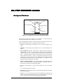
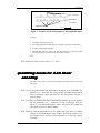
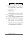
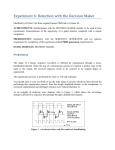
PCM ENCODING
PREPARATION................................................................................ 2
PCM ......................................................................................... 2
PCM encoding....................................................................................... 2
the PCM ENCODER module.................................................... 4
front panel features................................................................................ 4
the TIMS PCM time frame .................................................................... 5
pre-calculations......................................................................... 5
EXPERIMENT.................................................................................. 5
patching up ............................................................................... 6
quantizing levels for 4-bit linear encoding.................................. 7
4-bit data format .................................................................................... 8
7-bit linear encoding.............................................................................. 8
companding........................................................................................... 8
periodic messages.................................................................................. 9
conclusions ............................................................................... 9
TUTORIAL QUESTIONS............................................................... 10
APPENDIX ..................................................................................... 11
Copyright © 2005 Emona Instruments Pty Ltd
D1-11-rev 2.0 - 1
PCM ENCODING
ACHIEVEMENTS: introduction to pulse code modulation (PCM) and the PCM
ENCODER module. Coding of a message into a train of digital
words in binary format.
PREREQUISITES: an understanding of sampling, from previous experiments, and
of PCM from course work or a suitable text. Completion of the
experiment entitled Sampling with SAMPLE & HOLD (in this Volume)
would be a distinct advantage.
ADVANCED MODULES: PCM ENCODER
PREPARATION
PCM
This is an introductory experiment to pulse code modulation - PCM.
The experiment will acquaint you with the PCM ENCODER, which is one of the
TIMS Advanced Modules. This module generates a PCM output signal from an
analog input message.
In this experiment the module will be used in isolation; that is, it will not be part of
a larger system. The formatting of a PCM signal will be examined in the time
domain.
A later experiment, entitled PCM decoding (in this Volume), will illustrate the
recovery of the analog message from the digital signal.
In another experiment, entitled PCM TDM (within Volume D2 - Further &
Advanced Digital Experiments), the module will be part of a system which will
generate a two-channel pulse code modulated time division multiplexed system
(PCM TDM).
PCM encoding
The input to the PCM ENCODER module is an analog message. This must be
constrained to a defined bandwidth and amplitude range.
The maximum allowable message bandwidth will depend upon the sampling rate to
be used. The Nyquist criterion must be observed.
D1-11 - 2
Copyright © 2005 Emona Instruments Pty Ltd
PCM encoding
The amplitude range must be held within the ± 2.0 volts range of the TIMS
ANALOG REFERENCE LEVEL. This is in keeping with the input amplitude
limits set for all analog modules.
A step-by-step description of the operation of the module follows:
1. the module is driven by an external TTL clock.
2. the input analog message is sampled periodically. The sample rate is
determined by the external clock.
3. the sampling is a sample-and-hold operation. It is internal to the module, and
cannot be viewed by the user 1. What is held is the amplitude of the analog
message at the sampling instant.
4. each sample amplitude is compared with a finite set of amplitude levels. These
are distributed (uniformly, for linear sampling) within the range ± 2.0 volts (the
TIMS ANALOG REFERENCE LEVEL). These are the system quantizing
levels.
5. each quantizing level is assigned a number, starting from zero for the lowest
(most negative) level, with the highest number being (L-1), where L is the
available number of levels.
6. each sample is assigned a digital (binary) code word representing the number
associated with the quantizing level which is closest to the sample amplitude.
The number of bits ‘n’ in the digital code word will depend upon the number of
quantizing levels. In fact, n = log2(L).
7. the code word is assembled into a time frame together with other bits as may be
required (described below). In the TIMS PCM ENCODER (and many
commercial systems) a single extra bit is added, in the least significant bit
position. This is alternately a one or a zero. These bits are used by subsequent
decoders for frame synchronization.
8. the frames are transmitted serially. They are transmitted at the same rate as the
samples are taken (but see Tutorial Question 3). The serial bit stream appears
at the output of the module.
9. also available from the module is a synchronizing signal FS (‘frame synch’).
This signals the end of each data frame.
1 the sample and hold operation is examined separately in the experiment entitled Sampling with SAMPLE &
HOLD in
this Volume.
Copyright © 2005 Emona Instruments Pty Ltd
D1-11 - 3
the PCM ENCODER module
front panel features
SLAVE
MASTER
SELECT CODING SCHEME
SYNC. MESSAGE
FS
v in
CLK
PCM DATA
Figure 2: front panel layout of the PCM ENCODER
The front panel layout of the module is shown in Figure 2. Technical details are
described in the TIMS Advanced Modules User Manual.
Note and understand the purpose of each of the input and output connections, and
the three-position toggle switch. Counting from the top, these are:
• SLAVE: not used during this experiment. Do not connect anything to this
input.
• MASTER: not used during this experiment. Do not connect anything to this
output.
• SYNC. MESSAGE: periodic, ‘synchronized’, message. Either sinusoidal, or
sinusoidal-like (‘sinuous’), its frequency being a sub-multiple of the MASTER
CLOCK (being any one of four frequencies selected by an on-board switch
SW2). A message synchronized to the system clock is convenient for obtaining
stable oscilloscope displays. Having a recognisable shape (but being more
complex than a simple sine wave) gives a qualitative idea of distortion during
the decoding process (examined in a later experiment). See Table A-1 in the
Appendix to this experiment for more details.
• SELECT CODING SCHEME: a three-position toggle switch which selects the
4-bit or 7-bit encoding scheme of the analog samples; or (together with an onboard jumper connection) the companding scheme.
• FS: frame synchronization, a signal which indicates the end of each data
frame.
• Vin:: the analog signal to be encoded.
• PCM DATA: the output data stream, the examination of which forms the major
part of this experiment.
• CLK: this is a TTL (red) input, and serves as the MASTER CLOCK for the
module. Clock rate must be 10 kHz or less. For this experiment you will use
the 8.333 kHz TTL signal from the MASTER SIGNALS module.
D1-11 - 4
Copyright © 2005 Emona Instruments Pty Ltd
PCM encoding
the TIMS PCM time frame
Each binary word is located in a time frame. The time frame contains eight slots of
equal length, and is eight clock periods long. The slots, from first to last, are
numbered 7 through 0. These slots contain the bits of a binary word. The least
significant bit (LSB) is contained in slot 0.
The LSB consists of alternating ones and zeros. These are placed (‘embedded’) in
the frame by the encoder itself, and cannot be modified by the user. They are used
by subsequent decoders to determine the location of each frame in the data stream,
and its length. See the experiment entitled PCM decoding (in this Volume).
The remaining seven slots are available for the bits of the binary code word. Thus
the system is capable of a resolution of seven-bits maximum. This resolution, for
purposes of experiment, can be reduced to four bits (by front panel switch). The 4bit mode uses only five of the available eight slots - one for the embedded frame
synchronization bits, and the remaining four for the binary code word (in slots 4, 3,
2, and 1).
prepre-calculations
You will be using an 8.333 kHz master clock. Answer Tutorial Question Q1 now,
before commencing the experiment.
EXPERIMENT
The only module required for this experiment is a TIMS PCM ENCODER.
It is not necessary, for this experiment, to become involved with how the PCM
ENCODER module achieves its purpose. What will be discovered is what it does
under various conditions of operation.
The module is capable of being used in two modes: as a stand-alone PCM encoder,
for one channel, or, with modifications to the data stream, as part of a two-channel
time division multiplexed (TDM) PCM system.
Operation as a single channel PCM encoder is examined in this experiment.
Before plugging the module in:
T1 select the TIMS companding A4-law with the on-board COMP jumper (in
preparation for a later part of the experiment).
T2 locate the on-board switch SW2. Put the LEFT HAND toggle DOWN and the
RIGHT HAND toggle UP. This sets the frequency of a message from
the module at SYNC. MESSAGE. This message is synchronized to a submultiple of the MASTER CLOCK frequency. For more detail see the
Appendix to this experiment.
Copyright © 2005 Emona Instruments Pty Ltd
D1-11 - 5
patching up
To determine some of the properties of the analog to digital conversion process it is
best to start with a DC message. This ensures completely stable oscilloscope
displays, and enables easy identification of the quantizing levels.
Selecting the 4-bit encoding scheme reduces the number of levels (24) to be
examined.
T3 insert the module into the TIMS frame. Switch the front panel toggle switch
to 4-BIT LINEAR (ie., no companding).
T4 patch the 8.333 kHz TTL SAMPLE CLOCK from the MASTER SIGNALS
module to the CLK input of the PCM ENCODER module.
T5 connect the Vin input socket to ground of the variable DC module.
T6 connect the frame synchronization signal FS to the oscilloscope ext. synch.
input.
T7 on CH1-A display the frame synchronization signal FS. Adjust the sweep
speed to show three frame markers. These mark the end of each
frame.
T8 on CH2-A display the CLK signal.
T9 record the number of clock periods per frame.
Currently the analog input signal is zero volts (Vin is grounded). Before checking
with the oscilloscope, consider what the PCM output signal might look like. Make
a sketch of this signal, fully annotated. Then:
T10 on CH2-B display the PCM DATA from the PCM DATA output socket.
Except for the alternating pattern of ‘1’ and ‘0’ in the frame marker slot, you might
have expected nothing else in the frame (all zeros), because the input analog signal
is at zero volts. But you do not now the coding scheme.
There is an analog input signal to the encoder. It is of zero volts. This will have
been coded into a 4-bit binary output number, which will appear in each frame. It
need not be ‘0000’. The same number appears in each frame because the analog
input is constant.
Your display should be similar to that of Figure 3 below, except that this shows five
frames (too many frames on the oscilloscope display makes bit identification more
difficult).
D1-11 - 6
Copyright © 2005 Emona Instruments Pty Ltd
PCM encoding
FS - end of frame marker
FS - frame synch
PCM data out
clock periods
LSB at end of frame
time
Figure 3: 5 frames of 4-bit PCM output for zero amplitude input
Knowing:
1. the number of slots per frame is 8
2. the location of the least significant bit is coincident with the end of the frame
3. the binary word length is four bits
4. the first three slots are ‘empty’ (in fact filled with zeros, but these remain
unchanged under all conditions of the 4-bit coding scheme)
then:
T11 identify the binary word in slots 4, 3, 2, and 1.
quantizing levels for 4
4--bit linear
encoding
You will now proceed to determine the quantizing/encoding scheme for the 4-bit
linear case.
T12 remove the ground connection, and connect the output of the VARIABLE DC
module to Vin. Sweep the DC voltage slowly backwards and forwards
over its complete range, and note how the data pattern changes in
discrete jumps.
T13 if you have a WIDEBAND TRUE RMS METER module use this to monitor
the DC amplitude at Vin - otherwise use the oscilloscope (CH1-B).
Adjust Vin to its maximum negative value. Record the DC voltage and
the pattern of the 4-bit binary number.
T14 slowly increase the amplitude of the DC input signal until there is a sudden
change to the PCM output signal format. Record the format of the
new digital word, and the input amplitude at which the change
occurred.
Copyright © 2005 Emona Instruments Pty Ltd
D1-11 - 7
T15 continue this process over the full range of the DC supply.
T16 draw a diagram showing the quantizing levels and their associated binary
numbers.
4-bit data format
From measurements made so far you should be able to answer the questions:
•
•
•
•
•
•
what is the sampling rate ?
what is the frame width ?
what is the width of a data bit ?
what is the width of a data word ?
how many quantizing levels are there ?
are the quantizing levels uniformly (linearly) spaced ?
7-bit linear encoding
T17 change to 7-bit linear encoding by use of the front panel toggle switch.
It would take a long time to repeat all of the above Tasks for the 7-bit encoding
scheme. Instead:
T18 make sufficient measurements so that you can answer all of the above
questions in the section titled 4-bit data format above. Making one or
two assumptions (such as ?) you should be able to deduce the coding
scheme used.
companding
This module is to be used in conjunction with the PCM DECODER in a later
experiment. As a pair they have a companding option. There is compression in the
encoder, and expansion in the decoder. In the encoder this means the quantizing
levels are closer together for small input amplitudes - that is, in effect, that the
input amplitude peaks are compressed during encoding. At the decoder the
‘reverse action’ is introduced to restore an approximate linear input/output
characteristic.
It can be shown that this sort of characteristic offers certain advantages, especially
when the message has a high peak-to-average amplitude characteristic, as does
speech, and where the signal-to-noise ratio is not high.
This improvement will not be checked in this experiment. But the existence of the
non-linear quantization in the encoder will be confirmed.
In a later experiment, entitled PCM decoding (in this Volume), it will be possible
to check the input/output linearity of the modules as a compatible pair.
D1-11 - 8
Copyright © 2005 Emona Instruments Pty Ltd
PCM encoding
T19 change to 4-bit companding by use of the front panel toggle switch.
T20 the TIMS A4 companding law has already been selected (first Task). Make
the necessary measurements to determine the nature of the law.
periodic messages
Although the experiment is substantially complete, you may have wondered why a
periodic message was not chosen at any time. Try it.
T21 take a periodic message from the SYNC. MESSAGE socket. This was set as the
second Task.
T22 adjust the oscilloscope to display the message. Record its frequency and
shape. Check if these are compatible with the Nyquist criterion;
adjust the amplitude if necessary with one of the BUFFER
AMPLIFIERS.
T23 now look at the PCM DATA output. Synchronize the oscilloscope (as
previously) to the frame (FS) signal. Display two or three frames on
CH1-A, and the PCM DATA output on CH2-A.
You will see that the data signal reveals very little. It consists of many overlaid
digital words, all different.
One would need more sophisticated equipment than is assumed here (a digital
analyzer, a storage oscilloscope, ability to capture a single frame, and so on) to
deduce the coding and quantizing scheme from such an input signal.
conclusions
What is the advantage of 7-bit over 4-bit encoding ? Of what use is companding ?
From your measurements alone these questions cannot be answered.
These and other questions will be addressed in the experiment entitled PCM
decoding (in this volume - but see the Tutorial Questions).
The findings of this experiment will be required in later PCM experiments. These
will involve decoding of the data stream, an investigation of companding, and time
multiplexing of the outputs from two PCM ENCODER modules.
Copyright © 2005 Emona Instruments Pty Ltd
D1-11 - 9
TUTORIAL QUESTIONS
Q1 from your knowledge of the PCM ENCODER module, obtained during
preparation for the experiment, calculate the sampling rate of the
analog input signal. Show that it is the same for both the 4-bit and
the 7-bit coding schemes. What can you say about the bandwidth of
an input analog signal to be encoded ?
Q2 define what is meant by the data ‘frame’ in this experiment. Draw a diagram
showing the composition of a frame for:
a) the 4-bit coding scheme
b) the 7-bit coding scheme
Q3 it is possible to transmit each frame at a much slower rate than it was
produced (and, of course, recover the original message as well).
Explain how this might be done. When might this be an advantage ?
Q4 explain why a DC message gives a stable oscilloscope display of the PCM
DATA output. Why is the display ‘unstable’ when a sine wave (for
example) is the message ?
Q5 for the 4-bit encoder draw a diagram showing the amplitude quantization
levels and the corresponding binary numbers used to encode them.
Describe how this information was obtained experimentally.
Q6 two PCM signals can be combined to produce a time division multiplexed
(PCM TDM) signal. With the measurements so far performed this
does not seem (and indeed, is not) possible with two PCM ENCODER
modules ! Why is this so ? Suggest what changes could be made to
the module to implement PCM TDM 2.
Q7 if you have studied the principles of companding in your course, describe its
advantages. Then, if not already done so, plot the shape of the TIMS
compression law introduced by the companding operation you
measured. Compare this with published information about the ‘A’
and ‘µ’ companding laws used respectively in Europe and the USA.
2 in a later experiment it will be seen that suitable modifications to the data stream have been introduced so
that a two-channel PCM TDM can be modelled.
D1-11 - 10
Copyright © 2005 Emona Instruments Pty Ltd
PCM encoding
APPENDIX
For a MASTER CLOCK of 8.333 kHz, Table A-1 below gives the frequencies of
the synchronized message at the SYNC. MESSAGE output for the setting of the
on-board switch SW2.
For other clock frequencies the message frequency can be calculated by using the
‘divide by’ entry in the Table.
These messages are periodic, but not necessarily sinusoidal in shape. The term
‘sinuous’ means sine-like.
LH toggle RH toggle
UP
DOWN
UP
DOWN
UP
UP
DOWN
DOWN
divide
clock by
freq with
8.333kHz
clock
approx. ampl.
and waveform
32
64
128
256
260.4 Hz
130.2 Hz
65.1 Hz
32.6 Hz
0.2 Vpp sine
2.0 Vpp sine
4.0 Vpp sinuous
4.0 Vpp sinuous
Table A-1
Copyright © 2005 Emona Instruments Pty Ltd
D1-11 - 11
D1-11 - 12
Copyright © 2005 Emona Instruments Pty Ltd