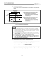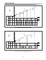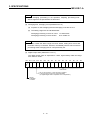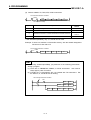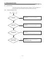
1
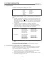
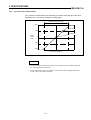
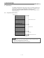
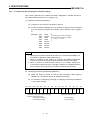
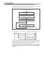
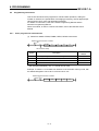
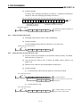
MELSEC A series Programmable Controller User´s Manual A68 AD MITSUBISHI ELECTRIC EUROPE B.V. FACTORY AUTOMATION • SAFETY PRECAUTIONS • (Read these precautions before using.) When using Mitsubishi equipment, thoroughly read this manual and the associated manuals introduced in this manual. Also pay careful attention to safety and handle the module properly. These precautions apply only to Mitsubishi equipment. Refer to the CPU module user's manual for a description of the PC system safety precautions. These SAFETY PRECAUTIONS "CAUTION". classify the safety precautions into two categories: "DANGER" and DANGER Procedures which may lead to a dangerous condition and cause death or serious injury if not carried out properly. CAUTION Procedures which may lead to a dangerous condition and cause superficial to medium injury, or physical damage only, if not carried out properly. Depending on circumstances, procedures indicated by CAUTION may also be linked to serious results. In any case, it is important to follow the directions for usage. Store this manual in a safe place so that you can take it out and read it whenever necessary. Always forward it to the end user. [System Design Precautions] DANGER • Safety circuits should be installed external to the programmable controller to ensure that the system as a whole will continue to operate safely in the event of an external power supply malfunction or a programmable controller failure. Erroneous outputs and operation could result in an accident. 1) The following circuitry should be installed outside the programmable controller: Interlock circuitry for the emergency stop circuit protective circuit, and for reciprocal operations such as forward/reverse, etc., and interlock circuitry for upper/lower positioning limits, etc., to prevent machine damage. 2) When the programmable controller detects an abnormal condition, processing is stopped and all outputs are switched OFF. This happens in the following cases • When the power supply module's over-current or over-voltage protection device is activated • When an error (watchdog timer error, etc.) is detected at the PC CPU by the self-diagnosis function. Some errors, such as input/output control errors, cannot be detected by the PC CPU, and there may be cases when all outputs are turned ON when such errors occur. In order to ensure that the machine operates safely in such cases, a failsafe circuit or mechanism should be provided outside the programmable controller. Refer to the CPU module user's manual for an example of such a failsafe circuit. 3) Outputs may become stuck at ON or OFF due to an output module relay or transistor failure. An external circuit should therefore be provided to monitor output signals whose incorrect operation could cause serious accidents. • A circuit should be installed which permits the external power supply to be switched ON only after the programmable controller power has been switched ON. Accidents caused by erroneous outputs and motion could result if the external power supply is switched ON first. • When a data link communication error occurs, the status shown below will be established at the faulty station. In order to ensure that the system operates safely at such times, an interlock circuit should be provided in the sequence program (using the communication status information). Erroneous outputs and operation could result in an accident. 1) The data link data which existed prior to the error will be held. 2) All outputs will be switched OFF at MELSECNET (II, /B, /10) remote I/Ostations. 3) At the MELSECNET/MINI-S3 remote I/O stations, all outputs will be switched OFF or output statuses will be held, depending on the E.C. mode setting. For details on procedures for checking faulty stations, and for operation statuses when such errors occur, refer to the appropriate data link manual. [System Design Precautions ] CAUTION • Do not bundle control lines or communication wires together with main circuit or power lines, or lay them close to these lines. As a guide, separate the lines by a distance of at least 100 mm, otherwise malfunctions may occur due to noise. When file register R that are outside the range are read, e.g. by a MOV instruction, the file register data will become FFFFH and use of this data will cause malfunctions. Take care not to use file registers that are outside the range when designing programs For details on instructions, refer to the Programming Manual. [Cautions on Mounting] CAUTION • Use the PC in an environment that conforms to the general specifications in the manual. Using the PC in environments outside the ranges stated in the general specifications will cause electric shock, fire, malfunction, or damage to/deterioration of the product. • Make sure that the module fixing projection on the base of the module is properly engaged in the module fixing hole in the base unit before mounting the module. Failure to mount the module properly will result in malfunction or failure, or in the module falling. • Extension cables should be securely connected to base unit and module connectors. Check for loose connection after installation A poor connection could result in contact problems and erroneous inputs/outputs. • Plug the memory card firmly into the memory card mounting connector. Check for loose connection after installation. A poor connection could result in erroneous operation. [Cautions on Wiring] DANGER • Switch off the external power supply before staring installation and wiring work Failure to do so could result in electrical shocks and equipment damage. • After installation and wiring is completed, be sure to attach the terminal cover before switching the power ON and starting operation Failure to do so could result in electrical shocks. CAUTION • Be sure to ground the FG and LG terminals, carrying out at least class 3 grounding work with a ground exclusive to the PC. Otherwise there will be a danger of electric shock and malfunctions. • Carry out wiring to the PC correctly, checking the rated voltage and terminal arrangement of the product. Using a power supply that does not conform to the rated voltage, or carrying out wiring incorrectly, will cause fire or failure. • Outputs from multiple power supply modules should not be connected in parallel. Failure to do so could cause the power supply module to overheat, resulting in a fire or module failure. • Tighten the terminal screws to the stipulated torque. Loose screws will cause short circuits, fire, or malfunctions. • Make sure that no foreign matter such as chips or wiring offcuts gets inside the module. It will cause fire, failure or malfunction. • Connectors for external connections should be crimped, pressure welded, or soldered in the correct manner using the correct tools For details regarding crimping and pressure welding tools, refer to the input/output module user's manual. A poor connection could cause shorts, fire, and erroneous operation. [Cautions on Startup and Maintenance] DANGER • Do not touch terminals while the power is ON. This will cause malfunctions. • Make sure that the battery is connected properly. Do not attempt to charge or disassemble the battery, do not heat the battery or place it in a flame, and do not short or solder the battery. Incorrect handling of the battery can cause battery heat generation and ruptures which could result in fire or injury. • Switch the power off before cleaning or re-tightening terminal screws. Carrying out this work while the power is ON will cause failure or malfunction of the module. CAUTION • In order to ensure safe operation, read the manual carefully to acquaint yourself with procedures for program changes, forced outputs, RUN,STOP,and PAUSE operations, etc., while operation is in progress. Incorrect operation could result in machine failure and injury. • Do not disassemble or modify any module. This will cause failure, malfunction, injuries, or fire. • Switch the power OFF before mounting or removing the module. Mounting or removing it with the power ON can cause failure or malfunction of the module. • When replacing fuses, be sure to use the prescribed fuse. A fuse of the wrong capacity could cause a fire. [Cautions on Disposal] CAUTION • Dispose of this product as industrial waste. IMPORTANT (1) Design the configuration of a system to provide an external protective or safety inter locking circuit for the PCs. (2) The components on the printed circuit boards will be damaged by static electricity, so avoid handling them directly. If it is necessary to handle them take the following precautions. (a) Ground your body and the work bench. (b) Do not touch the conductive areas of the printed circuit board and its electrical parts with nongrounded tools, etc. Under no circumstances will Mitsubishi Electric be liable or responsible for any consequential damage that may arise as a result of the installation or use of this equipment. All examples and diagrams shown in this manual are intended only as an aid to understanding the text, not to guarantee operation. Mitsubishi Electric will accept no responsibility for actual use of the product based on these illustrative examples. Owing to the very great variety in possible applications of this equipment, you must satisfy yourself as to its suitability for your specific application. REVISIONS *The manual number is given on the bottom left of the back cover. Print Date *Manual Number Revision Nov., 1985 IB (NA) 66054-A First edition Jan., 1986 IB (NA) 66054-B Correction Sections 2.2, 2.4, 4.1, 5.3.1, 6.3.1, 6.3.7, 8.2.3 Addition Section 3.3, IMPORTANT Feb., 1986 IB (NA) 66054-C Correction Sections 3.1, 4.1, 8.2.5 Aug., 1986 IB (NA) 66054-D Deletion Sections 2.4, 5.1, 5.2 Correction Items are changed meeting A0J2CPU Jun., 1987 IB (NA) 66054-E Correction Sections 2.1, 3.2.2, 4.2 Apr., 1988 IB (NA) 66054-F Correction Sections 5.2.1, 5.3.1 May., 1988 IB (NA) 66054-G Applicable CPU model names are reviewed (A1N, A2N, A2N-S1, A3NCPU, A3HCPU) Jul., 1988 IB (NA) 66054-H "Instructions for Strategic Materials" added Mar., 1989 IB (NA) 66054-I Correction Section 5.2.1 Jul., 1989 IB (NA) 66054-J Addition Section 4.2 INTRODUCTION Thank you for choosing the Mitsubishi MELSEC-A Series of General Purpose Programmable Controllers Please read this manual carefully so that the equipment is used to its optimum. A copy of this manual should be forwarded to the end user. Manual name : A68AD USERS IB(NA) 66054J Section Revision Contents Intro important Safety 1 2 3 4 5 6 Manual page NO. 1-1 2-1 to 2-2 3-1 3-3 to 3-10 3-11 to 3-15 4-1 to 4-2 5-1 6-1 to 6-7 7-1 to 7-3 8-1 to 8-7 APP-1 File name Revision Contents Intro Important Safety 010000jc 020000jc 030000jc 030200ac 030300jc 040000jc 050000jc 060000jc 070000ac 080000ac A10000ac Designer data file name P4d2 da,db, dc, dd, df, dg, dh, dj g3-9 P4d2 P4d4 L6-7n, L6-2, L6-5, L6-4, L6-6a, L6-6b, L6-7 Appd 2 CONTENTS 1. GENERAL DESCRIPTION...................................................................................................................1 − 1 2. SYSTEM CONFIGURATION ....................................................................................................2 − 1 ∼ 2 − 2 3. 2.1 Overall Configuration ..................................................................................................................2 − 1 2.2 Applicable System ......................................................................................................................2 − 2 2.3 Precautions when Using One A68AD Module with Multiple Channels.......................................2 − 2 SPECIFICATIONS ..................................................................................................................3 − 1 ∼ 3 − 15 3.1 General Specifications ................................................................................................................3 − 1 3.2 Performance Specifications ........................................................................................................3 − 2 3.2.1 4. 5. 7. 3.2.2 I/O conversion characteristics........................................................................................3 − 3 3.2.3 Digital I/O system...........................................................................................................3 − 7 3.3 I/O List with Respect to Programmable Controller CPU ...........................................................3 − 11 3.4 Buffer Memory ..........................................................................................................................3 − 12 3.4.1 Assignment of buffer memory ......................................................................................3 − 12 3.4.2 Contents and data configuration of buffer memory .....................................................3 − 13 HANDLING ...............................................................................................................................4 − 1 ∼ 4 − 2 4.1 Handling Instructions ..................................................................................................................4 − 1 4.2 Nomenclature..............................................................................................................................4 − 2 INSTALLATION ....................................................................................................................................5 − 1 5.1 6. Specifications.................................................................................................................3 − 2 Wiring..........................................................................................................................................5 − 1 5.1.1 Wiring instructions .........................................................................................................5 − 1 5.1.2 Unit connection example................................................................................................5 − 1 5.1.3 Maintenance and Inspection..........................................................................................5 − 1 PROGRAMMING ......................................................................................................................6 − 1 ∼ 6 − 8 6.1 Initial Setting ...............................................................................................................................6 − 1 6.2 Programming Instructions ...........................................................................................................6 − 3 6.2.1 Basic programs for read and write.................................................................................6 − 3 6.2.2 Setting the number of channels .....................................................................................6 − 5 6.2.3 Setting of averaging time or averaging count.................................................................6 − 5 6.2.4 Averaging processing specification................................................................................6 − 5 6.2.5 Read of digital output value ...........................................................................................6 − 6 6.2.6 Read and reset of write data error code ........................................................................6 − 6 6.2.7 Application circuit examples...........................................................................................6 − 7 TEST OPERATION AND CALIBRATION ................................................................................7 − 1 ∼ 7 − 3 7.1 Offset/Gain Setting......................................................................................................................7 − 1 7.2 Checks before Staring ................................................................................................................7 − 3 −i− 8. TROUBLESHOOTING..............................................................................................................8 − 1 ∼ 8 − 7 8.1 Write Data Error Code List..........................................................................................................8 − 1 8.2 Troubleshooting...........................................................................................................................8 − 2 8.2.1 Troubleshooting flow chart .............................................................................................8 − 2 8.2.2 Flow chart used when "RUN" LED has flickered ...........................................................8 − 3 8.2.3 Flow chart used when "RUN" LED has turned off .........................................................8 − 4 8.2.4 Flow chart used when digital output value cannot be read ...........................................8 − 5 8.2.5 Flow chart used when data, such as the number of channels, cannot be written.........8 − 7 APPENDIX ............................................................................................................................................. APP − 1 External View...........................................................................................................................................APP − 1 − ii − 1. GENERAL DESCRIPTION MELSEC-A 1. GENERAL DESCRIPTION This User's Manual describes the specifications, handling programming procedures, etc. for the A68AD analog-digital converter module (hereinafter referred to as "A68AD") which is used in combination with the MELSEC-A series CPU module. Refer to the following manuals as necessary when using the A68AD: A1N, A2N, A3NCPU User's Manuals. ACPU Programming Manual A0J2 (CPU Module, I/O Module) User's Manual A0J2 Programming Manual Data Link System User's Manual POINT In this manual, the I/O allocation numbers of the A68AD as seen from the P CPU are those when a building block type CPU is used and the A68AD is loaded in slot No.0 of the main base unit. If the A68AD is loaded in a slot other than slot No.0, or A0J2CPU is used, determine the allocation numbers of the A68AD using the I/O allocation method in the Programming Manual. The following generic terms are used for CPU types in this manual. (1) PC CPUs A1, A2, A2-S1, A3CPU(P21/R21) A1N, A2N, A2N-S1, A3NCPU(P21/R21) A3HCPU(P21/R21) A0J2CPU(P23/R23) (2) Building block type CPUs A1, A2, A2-S1, A3CPU(P21/R21) A1N, A2N, A2N-S1, A3NCPU(P21/R21) A3HCPU(P21/R21) (3) Compact type CPUs A0J2CPU(P23/R23) (4) ACPU A1, A2, A2-S1, A3CPU(P21/R21) A1N, A2N, A2N-S1, A3NCPU(P21/R21) A3HCPU(P21/R21) A0J2CPU(P23/R23) 1−1 2. SYSTEM CONFIGURATION MELSEC-A 2. SYSTEM CONFIGURATION Overall Configuration The overall configuration is shown in Fig. 2.1. Type Type Building type CPU module Compact type CPU module A68AD RUN 1 0 9 8 4 3 CH. 2 7 5 2.1 6 OFFSET GAIN TEST 1 3 2 3 V+ C H 1 C H 3 C H 5 C H 6 C H 7 5 6 7 FG I+ COM FG V+ I+ COM 8 9 10 11 12 13 14 15 FG V+ C H 4 4 I+ COM V+ C H 2 I+ COM 16 17 18 19 FG V+ I+ COM FG V+ I+ COM 20 21 22 23 24 25 26 27 FG V+ I+ COM 28 29 30 31 FG 32 C H 8 33 I+ COM 34 35 FG 36 37 ANALOG GND AD 10 V 0 4~20mA Type A38B A35B A32B Main base unit Type Type 38 A68AD A/D converter module AC06B AC12B AC30B Type Extension base unit A0J2C01 A0J2C03 A0J2C10 I/O cable Type A0J2 I/O module Extension cable A68B A65B A58B A55B Type A68B A65B A58B A55B Type Extension base unit Fig. 2.1 Overall Configuration Diagram 2−1 Type A0J2C04B A0J2C10B Extension cable 2. SYSTEM CONFIGURATION MELSEC-A 2.2 Applicable System The A68AD can be used with the following CPU modules: Applicable models A0J2CPU A1CPU A2CPU A2CPU-S1 A3CPU A3HCPU A1NCPU A2NCPU A2NCPU-S1 A3NCPU The A68AD can be loaded into any slot of a base unit with the exceptions given below: (1) If possible, avoid loading the A68AD into an extension base unit without a power supply module (type A5 extension base units) because the power supply may be insufficient. If the A68AD is loaded in such a base unit, see the CPU module User's Manual for details on selecting an appropriate power supply module and extension cable. (2) In a data link system, the A68AD can be loaded at a master station, localstation, or remote I/O station, but the CPU modules that can be used at master stations and local stations are restricted to those indicated below. (The same restrictions apply for coaxial link and fiber optic link systems). Master station A1CPUP21/R21 A2CPUP21/R21 A2CPUP21/R21-S1 A3CPUP21/R21 A3HCPUP21/R21 Local station A0J2CPUP23/R23 A1CPUP21/R21 A2CPUP21/R21 A2CPUP21/R21-S1 A3CPUP21/R21 A3HCPUP21/R21 A1NCPUP21/R21 A2NCPUP21/R21 A2NCPUP21/R21-S1 A3NCPUP21/R21 A1NCPUP21/R21 A2NCPUP21/R21 A2NCPUP21/R21-S1 A3NCPUP21/R21 (3) When use with A3CPU(P21/R21), cannot install at the final slot of 7th extension base. For the processing time (reading/writing) when using the A68AD in a data link system, refer to the Data Link User's Manual. 2.3 Precautions when Using One A68AD Module with Multiple Channels The A68AD isolates the input terminals from the PC power supply by photocoupler, but there is no isolation between channels. When using multiple channels with a single module, pay attention to the following points. (1) Since the COM terminals for analog input are connected internally, make the voltage level or current level for the COM terminals the same. (2) If the COM terminals do not have the same level, use another A68AD, or isolate the channels externally for analog input. 2−2 3. SPECIFICATIONS MELSEC-A 3. SPECIFICATIONS This chapter describes the general specifications and performance specifications of the A68AD. 3.1 General Specifications The general specifications of A68AD are indicated in Table 3.1. Item Specifications Operating ambient temperature 0 to 5 °C Storage ambient temperature -20 to 75 °C Operating ambient humidity 10 to 90 %RH, no condensation Storage ambient humidity 10 to 90 %RH, no condensation Vibration resistance Conforms *1 to JIS C0911 Frequency Acceleration Amplitude Sweep Count 10 to 50 Hz 0.075 mm 10 times 55 to 150 Hz 1g *(1 octave/minute) Shock resistance Conforms to JIS C 0912 (10 g × 3 times in 3 directions) Noise durability By noise simulator 1500 Vpp noise voltage, 1 µs noise width and 25 to 60 Hz noise frequency Dielectric withstand voltage 500 VAC for 1 minute across batch of DC external terminals and ground Insulation resistance 5 MΩ or larger by 500 VDC insulation resistance tester across batch of AC external terminals and ground Grounding Class 3 grounding Operating ambience To be free from corrosive gases. Dust should be minimal. Cooling method Self-cooling Table 3.1 General Specifications REMARK One octave marked * indicates a change from the initial frequency to double or half frequency. For example, any of the changes from 10 Hz to 20 Hz, from 20 Hz to 40 Hz, from 40 Hz to 20 Hz, and 20 Hz to 10 Hz are referred to as one octave. *1 JIS : Japanese Industrial Standard 3−1 3. SPECIFICATIONS MELSEC-A 3.2 3.2.1 Performance Specifications Specifications Item Analog input Digital output Specifications Selection depends on input terminals Voltage: -10 to 0 to + 10 VDC (Input resistance : 30 kΩ) Current: + 4 to + 20m ADC (Input resistance : 25 Ω) *-20 to 0 to + 20 mA ca also be used for current input. A CPU: 16-bit, signed binary (-2048 to +2047) I/O characteristics Analog Input +10 V +5 V or + 20 mA 0 V or + 4 mA Digital Output +2000 +1000 -5 V or – 12 mA -10 V -1000 -2000 ± 0 Voltage: 5 mV (1/2000) Current: 20 µA (1/1000) Maximum resolution Overall accuracy Within ± 1 % (Accuracy with respect to the maximum value) Maximum conversion speed Maximum 2.5 ms/channel Absolute maximum input Voltage: ± 15 V Current: ± 30 mA Number of analo input points 8 channels/module Insulation method Photocoupler insulation between output terminals and PC power (Non-insulated between channels) Number of I/O points 32 points Connection terminal 38-point terminal block Applicable wire size 0.75 to 2 mm (Applicable tightening torque: 7 kg/cm) Applicable solderless terminal V1.25-3, V1.25-YS3A, V2-S3, V2-YS3A Internal current consumption (5 V) 0.9 A Weight 0.6 kg (1.32 lb) 2 Table 3.2 Performance Specifications POINT Analog input allowed for maximum resolution and overall accuracy, is from -10 to 0 to +10 V or from -20 to 0 to +20 mA. 3−2 3. SPECIFICATIONS MELSEC-A 3.2.2 I/O conversion characteristics I/O conversion characteristics are dictated by the offset value and gain value set in test mode. Fig. 3.1 shows an example for voltage input. Practical analog input range 2047 Gain value 1000 Offset value Digital output value 0 -1000 -2048 -15 -10 0 10 15 Analog input voltage (V) Fig. 3.1 I/O Conversion Characteristics REMARKS 1. The offset value is the analog input (voltage or current) value at which the digital output value is 0. Set the offset value in test mode. 2. The gain value is the analog input (voltage or current) value at which the digital output value is 1000. Set the gain value in test mode. 3−3 3. SPECIFICATIONS MELSEC-A (1) Voltage input characteristic Fig. 3.2 shows the voltage characteristics for three different offset/gain combinations. Practical analog input range 2047 1) 2) 1000 Digital output value 0 5 -5 -2048 -15 -10 0 3) 10 15 Analog input voltage (V) The offset/gain setting in the figure at left is as follows. (1) When the offset value is 0 V and the gain value is 2.5 V, the characteristic is as indicated by 1). Example: When the analog input value is 3 V, the digital output value is 1200. When the analog input value is –3 V, the digital output value is -1200. (2) When the offset value is 0 V and the gain value is 5 V, the characteristic is as indicated by 2). Example: When the analog input value is 3 V, the digital output value is 600. When the analog input value is –3 V, the digital output value is -600. (3) When the offset value is –5 V and the gainvalue is 10 V, the characteristic is as indicated by 3). Example: When the analog input value is 3 V, the digital output value is 533. When the analog input value is –3 V, the digital output value is 133. Fig. 3.2 Voltage Input Characteristic POINTS 1. When the input voltage is in the range from -10 to 0 to +10 V, the maximum resolution and overall accuracy are within the quoted range of performance specifications. However, if this range is exceeded, resolution and accuracy will be impaired. 2. If an analog input corresponding to a digital output value of more than +2047 or less than -2048 is applied, the digital output value will not exceed +2047 or -2048. 3. Do not apply ±15 V or more. This will damage the module. 4. In offset/gain setting, the offset value should always be less than the gain value. If the offset value is greater than or equal to the gain value, the digital output value will be unpredictable. 3−4 3. SPECIFICATIONS MELSEC-A (2) Current input characteristic Fig. 3.3 shows the current characteristics for two different offset/gain combinations. Practical analog input range 2047 1) 1000 Digital output value 0 4 -2048 -30 -20 2) 0 20 30 The offset/gain setting in the figure at left is as follows. (1) When the offset value is 0 mA and the gain value is 5 mA, the characteristic is as indicated by 1). Example: When the analog input value is 7 mA, the digital output value is 1400. When the analog input value is –3 mA, the digital output value is -600. (2) When the offset value is 4 mA and the gain value is 20 mA, the characteristic is as indicated by 2). Example: When the analog input value is 7 mA, the digital output value is 187. When the analog input value is –3 mA, the digital output value is -437. Analog input current (mA) Fig. 3.3 Current Input Characteristic POINTS 1. When the input current is in the range from -20 to 0 to +20 mA, the maximum resolution and overall accuracy are within the quoted range of performance specifications. However, if this range is exceeded, resolution and accuracy will be impaired. 2. If an analog input, corresponding to a digital output value of more than +2047 or less than -2048 is applied, the digital output value will not exceed +2047 or -2048. 3. Do not apply ±30 mA or more. This will damage the module. 4. In offset/gain setting, the offset value should always be less than the gain value. If the offset value is greater than or equal to the gain value, the digital output value will be unpredictable. (3) Relation between offset/gain setting and digital output value The maximum resolution of the A68AD is 5 mV in voltage and 20 µA in current Maximum resolution may be found using the following expression: (Gain value) - (offset value) < (maximum resolution) 1000 Fig. 3.4 and 3.5 show the relation between the offset/gain setting and the digital output value for the offset/gain settings in Fig. 3.2 and 3.3. 3−5 3. SPECIFICATIONS MELSEC-A 1.000 999 998 997 996 995 994 993 992 991 990 Digital output value NO 1) Voltage Input Offse t 0 2), 3) * 1) Gain 2.475 to 2.480 2.480 to 2.485 2.485 to 2.490 2.490 to 2.495 2.495 to 2.500 2.500 to 2.505 2.5 4.950 4.955 4.960 4.965 4.970 4.975 4.980 4.985 4.990 4.995 to to to to to to to to to to 4.955 4.960 4.965 4.970 4.975 4.980 4.985 4.990 4.995 5.000 9.850 9.865 9.880 9.895 9.910 9.925 9.940 9.955 9.970 9.985 10.000 to to to to to to to to to to to 9.865 9.880 9.895 9.910 9.925 9.940 9.955 9.970 9.985 10.000 10.015 2) 0 5 3) -5 10 5.000 to 5.005 or more at top to Less than at bottom *: For 1), (gain value - offset value)/1000< 5 mV, so the digital value does not increase or decrease in units of one count. Fig. 3.4 Voltage Input and Digital Output Value 1.000 999 998 997 996 995 994 993 992 991 990 Digital output value ON Current Input 1) 2) Offse t 0 4 * 2) * 1) Gain 5 20 19.84 to 19.86 4.96 to 4.98 19.86 19.88 19.90 to to to 19.88 19.90 19.92 4.98 to 5.00 19.92 to 19.94 19.94 to 19.96 5.00 to 5.02 19.96 to 20.00 20.00 to 20.02 or more at top to Less than at bottom *: For 1) and 2), since (gain value - offset value)/1000 < 2 µA, the digital value does not always increase or decrease in units of one count. Fig. 3.5 Current Input and Digital Output Value 3−6 3. SPECIFICATIONS MELSEC-A 3.2.3 Digital I/O system The digital output value of the A68AD is determined by the following: (1) I/O conversion characteristics: Offset value Gain value The digital output value depends on the offset value and gain value which have been set in test mode. (2) A/D conversion system: Sampling processing Averaging processing in terms of count .....................................1 to 4000 times Averaging processing Averaging processing in terms of time .....................................20 to 10000 ms 1) Sampling processing The analog input values are converted to digital output values one by one and the digital output values are stored in the buffer memory. 2) Averaging processing The A68AD makes the A/D conversion for any channels to which averaging processing has been specified from the programmable controller CPU. Using a preset count or a preset period of time, an average is calculated (excluding the maximum value and the minimum value,) and stored to the buffer memory. If the processing count is specified as two or less, sampling processing is applied. 3−7 3. SPECIFICATIONS MELSEC-A POINT The A68AD may sample data in any one of three ways. These sampling methods can be applied separately to any channel. The sampling process is controlled by the A68AD's own CPU, but must be specified from the programmable controller CPU. (This is fully explained in section 3.4.1) Method 1 Sampling Processing: This is the most commonly used sampling procedure. As the A68AD's CPU scans each channel, the value appearing at that instant is written to the buffer memory as a digital value. The timing of this sampling depends on the number of channels used, and may be found from the following expression: Processing time Number of channels used = × 2.5 (ms/channel) (Where the maximum conversion speed is taken as 2.5 ms/channel) Example 1: Number of channels = 5 Processing time = 5 × 2.5 ms = 12.5 ms Method 2 Averaging processing by specifying time: In this case the CPU takes a number of samples of the data at each channel and than calculates the average value over the specified time period. The number of samples taken depends on the number of channels and the time setting. If is calculated as follows: (Time setting) (Processing count) = (Number of channels) × 2.5 ms - (I) Example 2: Time setting = 1000ms, 4 channels (Processing count) = 1000 = 100 samples. 4 × 2.5 (Where maximum conversion speed = 2.5 ms/channel) Method 3 Averaging processing by specifying a number of counts: This is similar to method 2 except that in this case the number of samples for the averaging process is specified. The processing time may be found from the following expression: 3−8 3. SPECIFICATIONS MELSEC-A Processing = time Count setting × Number of channels × 2.5 ms Example 3: Count setting = 500, 4 channels Processing time = 500 × 4 × 2.5 = 500 ms - (II) (Where maximum conversion speed = 2.5 ms/channel) A) Analog/Digital Output B) Average value calculated for 25 samples D) C) Average value calculated for 10 samples 0 100 200 300 400 500 600 700 800 Time (ms) Fig. 3.6 Graph showing variations between output values for different sampling methods. Refering to the graph in Fig. 3.6 Trace A) represents a steadily rising analog input signal. Trace B) represents the digital output obtained when method 1, sampling processing, is used. In this case the output value would be susceptible to variations due to any noise present on the analog signal. Trace C) represents the digital output obtained when time based averaging is used. In this case the number of channels was taken as 4 and the sampling time as 100 ms. Hence the processing count (from equation I) is: 100 = 10 samples 4 × 2.5 3−9 3. SPECIFICATIONS MELSEC-A 10 samples are therefore taken every 100 ms and an average calculated. This average is then output as a digital value while the CPU takes the next 10 samples. Note that the allowable time setting range is 20 → 10000 ms which is equivilant to 2 → 1000 samples (with 4 channels). Trace D) represents the digital output obtained when count based averaging is used. Again, the number of channels was taken as 4, the count setting was 25, the processing time, from equation II is 25 × 4 × 2.5 = 250 ms One sample is therefore taken every 10 ms, and after 25 samples have been taken, the average value is used for the digital output while the next 250 are being sampled. Note that the allowable count setting range is 1 → 4000 which is equivilant to 40 → 40000 ms (with 4 channels). 3 − 10 3. SPECIFICATIONS MELSEC-A 3.3 I/O List with Respect to Programmable Controller CPU The I/O signals of the A68AD with respect to a programmable controller CPU are as indicated below. Numbers for X and Y are determined by the slot occupied by the A68AD and the number of points of the other I/O units The I/O numbers indicated below are used when the A68AD module is loaded into slot No. 0 of the main base unit. (1) Input signals with respect to programmable controller CPU, 32 points from X0 to 1F. Input Signal Description X0 Watch dog timer error Turns on if a watch dog timer error occurs in the A68AD. X1 A/D conversion ready (1) Turns on when A/D conversion is ready (not in test mode) after the power is turned on or the programmable controller CPU is reset. Turns off in test mode. (2) Used as an interlock when read or write is performed from the programmable controller CPU to the A68AD. X2 to X1F Not used REMARK A/D conversion ready indicates that a digital output value has been stored into the buffer memory after the A/D conversion of all eight channels has been completed. (2) Output signals with respect to programmable controller CPU, 32 points from Y0 to 1F. Output Signal Description Y0 to Y1F Not used IMPORTANT Outputs Y0 to Y1F are reserved, they should not be used in the sequence program. If these output signals are used (turned ON/OFF) in a sequence program, it will not be possible to guarantee correct functioning of the A68AD. If the A68AD is used in a remote I/O rack, however, inputs Y0E and Y0F may be set and reset in the sequence program to allow "hand shaking" with the CPU. For details, refer to the Data Link System User's Manual. 3 − 11 3. SPECIFICATIONS MELSEC-A 3.4 Buffer Memory The A68AD is equipped with a buffer memory (which is not battery backed) for the communication of data with a programmable controller CPU. Explanation will be given for the assignment and data configuration of this buffer memory. For the read and write operation procedures by the sequence program, refer to Chapter 6 (page 6-1). 3.4.1 Assignment of buffer memory Address (Decimal) 0 Number of channels 1 Averaging processing specification 2 CH1 averaging time, count 3 CH2 averaging time, count 4 CH3 averaging time, count 5 CH4 averaging time, count 6 CH5 averaging time, count 7 CH6 averaging time, count 8 CH7 averaging time, count 9 Read and write from CPU CH8 averaging time, count 10 CH1 digital output value 11 CH2 digital output value 12 CH3 digital output value 13 CH4 digital output value 14 CH5 digital output value 15 CH6 digital output value 16 CH7 digital output value 17 CH8 digital output value Read from CPU 18 Not used to 33 34 Read and write from CPU Write data error code All 16 bit data. POINT The addresses 10 to 33 of buffer memory are areas exclusively used for reading from a programmable controller CPU. Writing to these addresses will cause mis operation. 3 − 12 3. SPECIFICATIONS MELSEC-A 3.4.2 Contents and data configuration of buffer memory This section describes the contents and data configuration of buffer memory for each item indicated in Section 3.4.1 (page 3-12). (1) Number of channels (Address 0) (a) At power-on, the number of channels is set to 8. (b) In order to reduce sampling time, the number of channels can be changed by in the sequence program. (For details, refer to Section 6.2.2 on page 64) Example: CH1 CH2 CH3 CH4 CH5 CH6 CH7 CH8 Used Vacant Used Used Vacant Vacant Vacant Vacant By setting the number of channels to 4, the sampling time is changed to 2.5ms × 4 = 10 ms. POINTS 1. Although the number of channels at power-on is set inside the A68AD, it is not written to address 0 of the buffer memory. 2. When 0 is written for the number of channels, the A68AD regards the number of channels as 8 when performing A/D conversion processing. 3. When a number of channels other than 0 to 8 is written, setting error occurs and the buffer memory is rewritten. However, the A68AD performs A/D conversion processing for the number of channels set previously. (2) Averaging processing specification (Address 1) (a) When the power is turned on and the A/D conversion ready signal of A68AD is on, all channels are set to sampling processing. (b) For selection of sampling processing or averaging processing use address 1 of the buffer memory. B15 B14 B13 B12 B11 B10 B9 B8 B7 B6 B5 B4 B3 B2 B1 B0 CH8 CH7 CH6 CH5 CH4 CH3 CH2 CH1 CH8 CH7 CH6 CH5 CH4 CH3 CH2 CH1 Specification of channel for which averaging processing will be performed 1: Averaging processing 0: Sampling processing 3 − 13 Specification of time/count 1: Time averaging 0: Count averaging 3. SPECIFICATIONS MELSEC-A POINT When averaging processing is not specified, sampling processing is set without regard to the specification of time/count. (3) Averaging time, averaging count (Addresses 2 to 9) (a) At power-on, the averaging time and averaging count are set to 0. (b) The setting ranges are as indicated below: Averaging processing in terms of count: 1 to 4000 times Averaging processing in terms of time: 20 to 10000 ms POINT If a value outside the above range has been written, setting error occurs and the buffer memory is rewritten. However, the A68AD performs A/D conversion processing at the averaging time or count previously set. (4) Digital output value (Addresses 10 to 17) The digital output value is expressed in 16-bit, signed binary within the range from -2048 to +2047. B15 B14 B13 B12 B11 B10 B9 B8 B7 B6 B5 B4 B3 1 0 Data section B11 to B14 change to 1 when the sign is negative (1 at B15) and to 0 when it is positive (0 at B15) (A negative digital value is expressed in 2's complement.) Sign bit 1: Negative 0: Positive 3 − 14 B2 B1 B0 3. SPECIFICATIONS MELSEC-A (5) Write data error code (Address 34) (a) When data is read from the programmable controller CPU, the A68AD makes a data range check for the number of channels used once only. When one of the values is outside the range, the A68AD sets an error code in 16-bit binary. For details of error codes, refer to Section 8.1 (page 8-1). (b) To reset an error code, write 0 from the programmable controller CPU. (c) When several error codes have occurred, t he data error code, witch has been detected by the A68AD first, is stored. The other errors are not stored. (d) If an error is reset without remedying the error, the data error code is set to 0 and the RUN LED of A68AD stops flickering (Section 4.2 on page 4-2). 3 − 15 4. HANDLING MELSEC-A 4. HANDLING This chapter describes the handling instructions, nomenclature, maintenance, and inspection of the A68AD. 4.1 Handling Instructions (1) Protect the A68AD and its terminal block from impact. (2) Do not touch or remove the printed circuit board from the case. (3) When wiring, ensure that no wire offcuts enter the module and remove any that do enter. (4) Tighten terminal screws as specified below. Screw TighteningTorque Range (kg⋅⋅cm) I/O terminal block terminal screw (M3 screw) 5 to 8 I/O terminal block mounting screw (M4 screw) 8 to 14 (5) To load the module onto the base, press the module against the base so that the hook is securely locked. To unload the module, push the catch on the top of the module, and after the hook is disengaged from the base, pull the module toward you. 4−1 4. HANDLING MELSEC-A Nomenclature Module fixing hook Hook for fixing the A68AD to the base unit A 68AD RUN CH. RUN LED 9 8 4 3 2 1 0 7 6 5 4.2 Indicates the operating status of A68AD. (Normal mode) ON: During normal operatio Flicker: At write data error or A68AD hardware error OFF: 5V power off or watch dog timer error (Test mode) ON: When the OFFSET switch or GAIN switch is located at the ON position. OFF: When both the OFFSET switch or GAI switch is located at the OFF position. OFFSET GAIN Test mode terminals TEST 1 Prior to offset/gain setting, connect together terminals 1 and 3. 3 2 V+ 4 3 C H 1 C H 2 5 I+ 6 COM 7 FG V+ I+ COM 9 Used to select a channel for the offset adjustment and gain adjustment (No processing at positions 0 and 9.) 11 FG 12 V+ 13 I+ C H 3 COM C H 4 COM 14 15 FG V+ 16 OFFSET switch 17 I+ 18 At the ON position, stores the applied analog input value into the A68AD as an offset value. 19 FG V+ C H 5 I+ COM C H 6 I+ COM 20 21 22 23 FG 24 V+ GAIN switch 25 26 At the ON position, stores the applied analog input value into the A68AD as a gain value. 27 FG V+ C H 7 CHANNEL select switch 8 10 28 29 I+ 30 COM 31 FG 32 C H 8 33 I+ 34 COM 35 FG 36 37 ANALOG GND AD 0 10 V 4~20mA 38 Switches marked (page 7-1). are valid only in test mode. For details, refer to Section 7.1 Terminal No. Signal Name Terminal No. 1 TEST 13 2 Not used 14 3 TEST 15 4 Not used 16 5 V+ 17 I+ 18 COM 19 8 FG 9 V+ 6 7 10 11 12 C H 1 C H 2 Signal Name V+ C H 3 Terminal No. I+ 26 COM 27 FG 28 V+ 29 I+ 30 COM 31 20 FG 32 21 V+ 33 I+ 22 COM 23 FG 24 4−2 C H 4 C H 5 Signal Name 25 I+ 34 COM 35 FG 36 V+ C H 6 I+ COM FG V+ C H 7 I+ COM FG V+ C H 8 I+ COM FG 37 Not used 38 Not used 5. INSTALLATION MELSEC-A 5. INSTALLATION 5.1 5.1.1 Wiring Wiring instructions Protect external wiring against noise with the following precautions: (1) Separate AC and DC wiring. (2) Separate main circuit and/or high voltage wiring from control and signal wiring. (3) Where applicable, ground the shielding of all wires to a common ground point. 5.1.2 Unit connection example (1) Voltage input Signal source: 0 to ±10 V CH1 *4 15 KΩ V+ +15 V 250 Ω I+ 15 KΩ COM 15 V FG *1 shield GND (2) Current input Signal source: 0 to ±20 mA *2 CH8 *3 15 KΩ V+ I+ COM 250 Ω 15 kΩ FG *1 shield ANALOG GND *5 *1: *2: *3: *4: For the cable, use a two-core twisted shielded wire. Indicates the input resistance of the A68AD. For current input, be sure to connect the terminals (V+) and (I+). If noise or ripple is generated at the external wiring, connect a capacitor of approximately 0.1 to 0.47 µF between terminals V and COM. *5: If there is excessive noise, ground the unit. POINT The FG terminal of the A68AD and the FG terminal of the power supply unit are not connected together internally. 5.1.3 Maintenance and Inspection The A68AD does not require any specific inspections, but in order to ensure that the system is always used under the optimum conditions, follow the inspection point in the CPU module User's Manual. 5−1 6. PROGRAMMING MELSEC-A 6. PROGRAMMING 6.1 Initial Setting Before analog to digital conversion begins it is necessary to write certain initial data to the buffer memory. This data consists of the number of channels used and specification of the sampling method required (See section 3.4.1) The most convenient way to write this data to the buffer memory is to use a single "TO" type instruction as shown in the example below: M9038 MOV K2 D0 MOVP H200 D1 MOVP K0 D2 MOVP K1000 D3 H000C K0 K4 X1 TOP D0 K2 D1 H200 D2 K0 D3 K1000 Buffer address 0 Loaded simmultaneously into buffer addresses 0-3 D0 Number of channels 1 Averaging processing specification 2 CH1 averaging time, count 3 CH2 averaging time, count 4 CH3 averaging time, count The above example sets the number of channels to 2 (i.e. D0), specifies channel 2 for count averaging (i.e. D1), and sets channel 2 count setting to 1000 (i.e. D3). The A68AD is located in the main base in the slot with head element number X/Y C0. 6−1 6. PROGRAMMING MELSEC-A The initial data may also be written using individual "TO" type instructions for each buffer address, in this case always execute in the following order: Start Set number of channels Set averaging time or averaging count Averaging processing specification Read of digital output value Fig.6.1 Initial Setting Procedure When this procedure is used, the previous example must be programmed as follows: TOP H000C K0 K2 K1 TOP H000C K2 TOP H000C K3 K1000 K0 K1 K1 TOP H000C K1 M200 K1 i.e. The count setting (K1000) is loaded into buffer address 3 before averaging processing specification, M200, is loaded into address 1. If this order is changed a write in error may occur. This will cause the run LED on the A68AD to flicker. Error status may also be found by monitoring buffer memory address 34. This error occurs because the A68AD is normally in run mode. If averaging processing specification is made, the A68AD immediatly looks for the relevant averaging data. If this data has not already been written to the unit an error is registered. 6−2 6. PROGRAMMING MELSEC-A 6.2 Programming Instructions This section describes basic programs for read and write operations, setting the number of channels, the specification of averaging processing, read of digital output value and write error code, and application examples. For details on instructions, refer to the ACPU Programming Manual and the A0J2CPU Programming Manual. When the module, is used in a remote I/O station, refer to the Data link User's Manual. 6.2.1 Basic programs for read and write (1) Read from A68AD: FROM, FROMP, DFRO, DFROP instructions FROM instruction execution condition FROMP n1 n2 D n3 A/D conversion ready Symbol Description Usable Device Number n1 Upper 2 digits of head I/O number assigned to A68AD K, H n2 Head address of buffer memory which stores data K, H D Head number of device which will stored read data *T, C, D, W, R n3 Number of words of data to be read K, H * With A0J2CPU(P23/R23), only T, C, and D can be used. Example: To read the 1 word data from address 10 of the buffer memory to D0, with the A68AD assigned to I/O X130 to 14F and Y130 to 14F FROM instruction execution condition X131 FROMP 6−3 H13 K10 D0 K1 6. PROGRAMMING MELSEC-A (2) Write to A68AD: TO, TOP, DTO, DTOP instructions TO instruction execution condition TOP n1 n2 S n3 A/D conversion ready Symbol Description Usable Device Number n1 Upper 2 digits of head I/O number assigned to A68AD K, H n2 Head address of buffer memory which will store data K, H D Head device number or constant where data to be written is stored. *T, C, D, W, R, K, H n3 Number of words of data to be written K ,H * With A0J2CPU(P23/R23), only T, C, and D can be used. Example: To write 8 to address 0 of the buffer memory, with the A68AD assigned to I/O X60 to 7F and Y60 to 7F TO instruction execution condition X61 TOP H6 K0 K8 K1 POINT When using A0J2CPU(P23/R23), pay attention to the following points when writing a program. (1) There are no FROMP,TOP, DFROP, or DTOP instructions. Use internal relays (M) for pulse conversion. (2) Constant (K, H) designations are not possible with TO instructions. Set the data inT, C, and D devices for writing. TO instruction execution condition X61 PLS M0 MOV K8 D0 K0 D0 K1 M0 TO 6−4 H6 6. PROGRAMMING MELSEC-A 6.2.2 Setting the number of channels (1) Set the number of channels 1 to 8. (2) Even if there is a vacant channel, the number o f channels must begin with channel 1. Set the number of the last channel used. (3) Program example To set the number of channels 3 Initial setting command X1 TOP 6.2.3 H0 K0 K3 K1 Setting of averaging time or averaging count (1) Set the averaging time or averaging count to each channel for which av eraging processing will be performed. (2) Be sure to set the averaging time or averaging count before specifying the averaging processing. (3) Set value Time: 20 to 10000 ms (Set the time in units of 10 ms.) Count: 1 to 4000 times (4) Program example To set the averaging time of 1000ms to channel 1 and the averaging count of 10 times to channel 3 Initial setting command X1 6.2.4 TOP H0 K2 K1000 K1 Write to channel 1 TOP H0 K4 K10 K1 Write to channel 3 Averaging processing specification (1) Specify the channels for which averaging processing will be performed, and also specify whether the processing method is count averaging or time averaging. (2) Be sure to specify the averaging processing method after setting the averaging time and/or averaging count. 6−5 6. PROGRAMMING MELSEC-A (3) Program example To specify time averaging processing at channel 1, sampling processing at channel 2, and count averaging processing at channel 3. CH8 CH7 CH6 CH5 CH4 CH3 CH2 CH1 CH8 CH7 CH6 CH5 CH4 CH3 CH2 CH1 0 0 0 0 0 1 0 1 0 6.2.5 H0 0 0 0 0 0 1 H501 Specification of time/count averaging Specification of channel for averaging processing Initial setting command X1 TOP 0 K1 H501 K1 Set averaging processing specification at the above value. Read of digital output value (1) The digital output value is read in 16-bit, signed binary. (2) Program example To read the digital output values of channels 1 to 3 to the D5 to 7. Digital output value read command X1 FROM 6.2.6 H0 K10 D5 K3 Read and reset of write data error code (1) Any error code is set at address 34 of the buffer memory in binary. For details, refer to Section 8.1 (page 8-1). (2) Only the first error code to occur, is stored. For details, refer to Section 3.4.2 (page 3-13). (3) Reset the error code from the programmable controller CPU. (4) Program example a) To read the error code to D3 and output it to Y100 to 107 in BCD. Error code read command X1 FROM b) H0 K34 D3 K1 BCD D3 K2Y100 K0 K1 Error code is read to D3. Error code is output to the Y100 to 107 in BCD code. To reset the error code Error code reset command X1 TOP H0 K34 6−6 0 is written to address 34 of buffer memory and error code is reset. 6. PROGRAMMING MELSEC-A 6.2.7 Application circuit examples (1) Checking the magnitude of the analog signal Program which turns on Y100 when the digital output value of channel 1 is 700 or more, turns on Y101 when it is between 600 and 700, and turns on Y102 when the value is negative. Execution command X1 Execution command X1 FROM Execution command Execution command <= K700 D0 <= K600 D0 > K0 D0 H0 K10 D0 X1 > K700 D0 X1 K1 Digital value of channel 1, is read to D0. Y 100 When digital output value is 700 or more, Y100 is turned on. Y 101 When digital output value is between 60 and 700, Y101 is turned on. Y 102 When digital output value is negative, Y102 is turned on. (2) Digital display of analog signal Program which outputs the digital output value of channel 1 to Y110 to 11F in BCD and turns on Y120 when that value is negative. Execution command X1 FROM Execution command K10 D0 X1 > Execution command H0 K0 D0 NEG K1 Digital value of channel 1, which is read to D0. Y 120 When D0 is negative, Y120 is turned on. D0 X1 BCD D0 6−7 K 4 Y 11 0 Negative value of D0 is converted into a positive value. The value of D0 is output to the Y110 t 11F in BCD. 6. PROGRAMMING MELSEC-A (3) Circuit which changes a gain to 4, 2, 1/2, and 1/4 times by program The digital output values are changed to the following gains; (all digital value must be > 0) Channel Channel Channel Channel 1: 2: 3: 4: 4 times 2 times 1/2 times 1/4 times Execution command X1 FROM H0 Digital output values of channels 1 to 4, which have been converted from analog values, are read to the D0 to 3. K10 D0 K4 SFL D0 K2 SFL D1 K1 The value of D0 is shifted 2 bits leftward and the digital output value of channel 1 is quadrupled. The value of D1 is shifted 1 bit leftward and the digital output value of channel 2 is doubled. SFR D2 K1 The value of D2 is shifted 1 bit rightward and the digital output value of channel 3 is halved. SFR D3 K2 The value of D3 is shifted 2 bits rightwar and the digital output value of channel 4 is quartered. 6−8 7. TEST OPERATION AND CALIBRATION MELSEC-A 7. TEST OPERATION AND CALIBRATION This chapter describes offset/gain setting. See also the A CPU User's Manual. 7.1 Offset/Gain Setting Change the output characteristics as follows. The unit is factory-set to an offset value of 0 V and a gain valueof 5 V. Start Connect terminals 1 and 3 to put the unit into TEST mode. Set the channel select switch on the front of unit to th required channel number. (Do not set to channel 0 or 9) Voltage adjustment? YES NO Current Voltage Apply offset voltage to the input terminal of channel to be calibrated and set the OFFSET switch to the up position. When the RUN LED turns on, the applied voltage is stored into the A68AD as the offset value. Switch on the required offset current to the channel to be calibrated and set the OFFSET switch to the up position. When the RUN LED turns on, the applied current is stored into the A68AD as the offset value. Apply gain voltage to the input terminal of channel to be calibrated and set the GAIN switch to the up position. When the RUN LED turns on, the applied voltage is stored into the A68AD as the gain value. Switch on the required gain current to the channel to be calibrated and set the GAIN switch to the up position. When the RUN LED turns on, the applied current is stored into the A68AD as the gain value. NO Have the setting of all channels been completed? YES Open the circuit across TEST terminals. Complete 7−1 7. TEST OPERATION AND CALIBRATION MELSEC-A POINTS 1. The offset value and gain value are stored in the A68AD and are not erased if the power is turned off. 2. Perform the offset/gain setting with the CPU in stop mode. When the unit is set to test mode, A/D conversion is stopped on all channels. Therefore, use the A/D conversion ready signal as an interlock. 3. Perform the offset/gain setting within the range -10 to 0 to +10 VDC or -20 to 0 to +20m ADC. If set outside this range, the maximum resolution and overall accuracy may not be within the ranges specified. 7−2 7. TEST OPERATION AND CALIBRATION MELSEC-A 7.2 Checks before Staring Number Checking Point 1 Loading of unit Description Is the I/O assignment correct? Has offset/gain been set for all channels used? 2 Offset/gain setting Are set values correct? Has the unit been returned to normal mod by opening the circuit across TEST terminals? Are terminal block connections correct? 3 Connection to A68AD Are terminal screws of terminal block tightened securely? Is the wire size correct? Table 7.1 Points for Checking 7−3 Check 8. TROUBLESHOOTING MELSEC-A 8. TROUBLESHOOTING This chapter describes errors, which may occur during the use of the A68AD, and troubleshooting procedures for such errors. 8.1 Write Data Error Code List The following three errors may occur during the write operation of the number of channels, averaging processing specification, averaging time, and averaging count The numeric value of the error code enclosed in indicates the channel number for which the error has occurred. Description Error Code A value other than 0 to 8 has been set as the number of channels. 01 A value other than 20 to 10000 ms has been set as an averaging time set value. 0 to 4 A value other than 1 to 4000 times has been set as an averaging count set value. 5 to 8 Table 8.1 Types of Write Data Error Codes POINT 1. 0 to 4 and 5 to 8 of write data error code are used only to make differentiation between averaging time and averaging count, respectively. The individual numerals do not have any significance. 2. When an error has occurred, check the write data error code, reset the error code, and then write the corrected data. (Refer to Section 3.4.2 on page 3-13.) Example: (1) Error code 32 has occurred Since the averaging time of channel 3 is wrong, change the value to within the range 20 to 10000 ms. (2) Error code 88 has occurred Since the averaging count of channel 8 is wrong, change the value to within the range 1 to 4000 times. 8−1 8. TROUBLESHOOTING MELSEC-A 8.2 Troubleshooting This section describes simple troubleshooting procedures for use of the A68AD. For problems relating to the CPU module, refer to the A CPU User's Manual. 8.2.1 Troubleshooting flow chart Error "RUN" LED of A68AD flickers. YES Section 8.2.2 "Flow chart used when "RUN" LED has flickered" YES Section 8.2.3 "Flow chart used when "RUN" LED has turned off" YES Section 8.2.4 "Flow chart used when digital output value cannot be read" YES Section 8.2.5 "Flow chart used when data, such as the number of channels, cannot be written" NO "RUN" LED of A68AD turns off. NO Digital output value cannot be read. NO Data, such as the number of channels, cannot be written. 8−2 8. TROUBLESHOOTING MELSEC-A 8.2.2 Flow chart used when "RUN" LED has flickered "RUN" LED flickers. Read write data error code from buffer memory. Channel setting error YES Check the number of channels. Compare this with the number of channels designated in Buffer Address 1. NO Please return the module to the nearest sales representative together with details of trouble. NO Setting error of averaging time or averaging count YES Check write data. Check if averaging time or averaging count has been set before averaging processing is specified. 8−3 8. TROUBLESHOOTING MELSEC-A 8.2.3 Flow chart used when "RUN" LED has turned off "RUN" LED turns off. Is the circuit open across test terminals 1 and 3? NO YES Open the circuit across test terminals 1 and 3. 1 "RUN" LED turns on. YES Monitor the input signal of A68AD watch dog timer error. NO Complete Watch dog timer error signal OFF NO YES Please return the module to the nearest sales representative together with details of trouble. Since possible cause is insufficient power capacity, calculate current consumption. Is power capacity OK? NO YES Recheck by loading and unloading the A68AD. Respecify power supply module used. 2 8−4 8. TROUBLESHOOTING MELSEC-A 8.2.4 Flow chart used when digital output value cannot be read Digital output value cannot be read. Read any error step number with peripheral equipment. Error occurs at the FROM instruction. NO YES Monitor D9008 by use of peripheral equipment. A68AD failure YES D9008 is 41. Check if the condition for executing FROM instruction is on. Check if the address of buffer memory in th FROM instruction is the address of digital output value of channel from witch data will be read. NO D9008 is 40. NO D9008 is 46. Check the I/O number of A68AD and th I/O number of FROM instruction. Read and check the setting number of channels for witch A/D conversion will be made. Check the wiring method for analog input (voltage or current) of A68AD. Check the stage number setting switch of extension base unit. Check if offset/gain setting is proper. CPU module failure NO Disconnect the wiring of analog input of A68AD, input voltage by use of stabilizin power or battery, and monitor digital output value. CPU module is normal. YES Base unit failure NO A68AD failure NO Base unit is normal. YES A68AD failure Please return the module to the nearest sales representative together with details of trouble. 8−5 If digital output value proper? YES External wiring is affected by noise. Examine grounding method. 8. TROUBLESHOOTING MELSEC-A REMARKS The following contents are written into D9008 when an error has occurred during execution of the FROM or TO instruction to the A68AD. Contents (BIN value) of Special Register D9008 CPU Status 40 41 Stop FROM and TO instructions cannot b executed. Hardware failure of A68AD (special function module), CPU unit, or base unit. Stop When the FROM or TO instruction has been executed, access has been made to the special function module but no answer is returned The accessed A68AD (special function module) has failed. Stop 46 Continuous operation can be performed by the setting of parameter. 8−6 Error and Cause Access has been made (FROM or TO instruction has been executed) to a slot where the A68AD (special function module) is not loaded The content of FROM or TO instruction is incorrect or the stage number setting of extension base unit is incorrect. 8. TROUBLESHOOTING MELSEC-A 8.2.5 Flow chart used when data, such as the number of channels, cannot be written The number of channels cannot be written. Read any error step number with peripheral equipment. Error occurs at the TO instruction. NO YES Read the write data error code and take corresponding corrective action. Monitor D9008 by use of peripheral equipment. D9008 is 40. YES NO D9008 is 41. A68AD failure YES NO Is CPU module normal? CPU module failure NO YES D9008 is 46. Check the I/O number of A68AD and the I/O number of TO instruction. Is base unit normal? Base unit failure NO Check the stage number setting switch of extension base unit. YES A68AD failure Please return the module to the nearest sales representative together with details of trouble. 8−7 APPENDIX MELSEC-A APPENDIX External View M3 (0.12) × 0.5 (0.02) × 6 (0.24) 2 (0.08) (Terminal screw) 4.2 (0.17) A68AD RUN CH. 2 3 4 1 0 9 8 7 5 6 OFFSET 8.6 (0.34) GAIN TEST 1 1 3 2 V+ 4 COM 6 3 C H 1 250 (9.84) Printed circuit board 7.2 (0.28) 7 FG V+ 8 COM 10 C H 2 I+ C H 3 I+ C H 4 5 I+ 9 11 FG V+ 12 COM 14 13 15 FG V+ 16 COM 18 17 I+ 19 FG V+ 20 C H 5 I+ COM 22 C H 6 I+ C H 7 C H 8 21 23 FG V+ 24 COM 26 25 27 FG V+ 28 I+ COM 30 29 31 FG V+ 32 COM 34 33 I+ 35 FG 36 37 ANALOG GND AD 0 10 V 4~20mA 10 (0.39) 6 (0.24) 4.2 (0.17) 106 (4.17) 38 18 (0.71) 25 (0.98) 37.5 (1.48) 131 (5.16) Unit : mm (inch) APP − 1