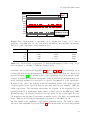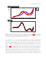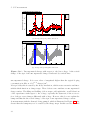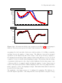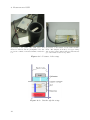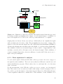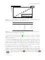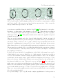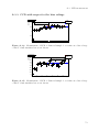
1
Master’s Thesis
Charakterisierung hochbestrahlter
polykristalliner Diamantsensoren für
ionisierende Strahlung
Characterisation of highly irradiated
polycrystalline diamond sensors for ionising
radiation
prepared by
Lars Graber
from Helmstedt
at the II. Physikalischen Institut
Thesis number:
II.Physik-UniGö-MSc-2011/01
Thesis period:
14th March 2011 until 13th September 2011
Supervisor:
Dr. Jens Weingarten
First referee:
Prof. Dr. Arnulf Quadt
Second referee:
Priv.Doz. Dr. Jörn Große-Knetter
Zusammenfassung
Hochbestrahlte Diamanten wurden auf ihre Eignung im Bezug auf die Verwendung als
Sensormaterial für Spurdetektoren untersucht. Hierfür wurden zwei Teststationen für C-V
und CCD-Messungen aufgebaut. Es zeigt sich, dass für hochbestrahlte Diamanten eine
Abhängigkeit der Kapazität von der angelegten Spannung besteht. Messungen der CCD
sind sowohl bei sehr niedriger CCD als auch für einen großen Spannungsbereich mit hoher
Präzision möglich. Graphitisierung von Diamant mittels eines Femtosekundenlasers wurde
zur Herstellung von Elektroden im Material für 3D-Sensoren untersucht.
Stichwörter: Hochenergiephysik, Diamant, Halbleitersensoren
Abstract
Highly irradiated diamonds are studied for their use as sensors for tracking detectors.
Two different setups for C-V and CCD measurement were built. For highly irradiated
diamonds a change of the capacitance with respect to the bias voltage is observed. Measurements of very low values of CCD are possible over a wide voltage range with high
statistical precision. Graphitisation of diamond using a femtosecond laser is tested for
the manufacturing of electrodes for 3D sensors.
Keywords: high energy physics, diamond, semiconductor sensors
iii
Contents
1. Introduction
1
2. Principles of solid state particle detectors
3
2.1. Energy loss of particles . . . . . . . . . . . . . . . . . . . . . . . . . . . . .
3
2.2. Sensor design . . . . . . . . . . . . . . . . . . . . . . . . . . . . . . . . . .
6
2.3. Read-out chain . . . . . . . . . . . . . . . . . . . . . . . . . . . . . . . . .
8
3. Diamond as a sensor material for particle detectors
11
3.1. Production of CVD diamond . . . . . . . . . . . . . . . . . . . . . . . . . . 11
3.2. Fundamental properties of diamond . . . . . . . . . . . . . . . . . . . . . . 13
3.3. Charge collection distance . . . . . . . . . . . . . . . . . . . . . . . . . . . 14
3.4. C-V measurement . . . . . . . . . . . . . . . . . . . . . . . . . . . . . . . . 16
4. Bulk segmentation
19
4.1. Motivation for new types of electrodes . . . . . . . . . . . . . . . . . . . . 19
4.2. Graphitisation of diamond . . . . . . . . . . . . . . . . . . . . . . . . . . . 21
5. C-V measurement
27
5.1. Experimental setup . . . . . . . . . . . . . . . . . . . . . . . . . . . . . . . 27
5.1.1. The diamond fixture . . . . . . . . . . . . . . . . . . . . . . . . . . 27
5.1.2. The B1505A Semiconductor Device Analyzer . . . . . . . . . . . . . 27
5.1.3. Diamond samples . . . . . . . . . . . . . . . . . . . . . . . . . . . . 30
5.2. Experimental results . . . . . . . . . . . . . . . . . . . . . . . . . . . . . . 31
5.2.1. Calibration . . . . . . . . . . . . . . . . . . . . . . . . . . . . . . . 31
5.2.2. Voltage sweep . . . . . . . . . . . . . . . . . . . . . . . . . . . . . . 34
6. Measurement of CCD
41
6.1. Experimental setup . . . . . . . . . . . . . . . . . . . . . . . . . . . . . . . 41
6.1.1. Data aquisition & analysis . . . . . . . . . . . . . . . . . . . . . . . 43
6.2. Experimental results . . . . . . . . . . . . . . . . . . . . . . . . . . . . . . 44
v
Contents
6.2.1. Calibration . . . . . . . . . . . . . . . . . . . . . . . . . . . . . . . 44
6.2.2. Evolution of CCD with time . . . . . . . . . . . . . . . . . . . . . . 46
6.2.3. CCD with respect to the bias voltage . . . . . . . . . . . . . . . . . 47
7. Graphitisation of diamond using a femtosecond laser
7.1. Experimental setup . . . . . . . . . . . . . . . . . . . .
7.2. Experimental results . . . . . . . . . . . . . . . . . . .
7.2.1. Calibration . . . . . . . . . . . . . . . . . . . .
7.2.2. Variable distance to the focal lens . . . . . . . .
7.2.3. Variable power of the laser beam . . . . . . . .
7.2.4. Variable duration of exposure . . . . . . . . . .
7.2.5. Depth of graphite spots . . . . . . . . . . . . .
.
.
.
.
.
.
.
.
.
.
.
.
.
.
.
.
.
.
.
.
.
.
.
.
.
.
.
.
.
.
.
.
.
.
.
.
.
.
.
.
.
.
.
.
.
.
.
.
.
.
.
.
.
.
.
.
.
.
.
.
.
.
.
.
.
.
.
.
.
.
.
.
.
.
.
.
.
55
55
56
56
58
58
60
61
8. Conclusion & Outlook
63
A. Appendix
A.1. Pictures of the diamond . . . . . . . . . . . .
A.2. C-V measurement . . . . . . . . . . . . . . . .
A.3. CCD measurement . . . . . . . . . . . . . . .
A.3.1. Calculation of activity after collimator
A.3.2. Shaper calibration . . . . . . . . . . .
A.3.3. CCD with respect to the bias voltage .
65
65
66
69
69
70
73
vi
.
.
.
.
.
.
.
.
.
.
.
.
.
.
.
.
.
.
.
.
.
.
.
.
.
.
.
.
.
.
.
.
.
.
.
.
.
.
.
.
.
.
.
.
.
.
.
.
.
.
.
.
.
.
.
.
.
.
.
.
.
.
.
.
.
.
.
.
.
.
.
.
.
.
.
.
.
.
.
.
.
.
.
.
.
.
.
.
.
.
.
.
.
.
.
.
Nomenclature
Acronyms
abbreviation
meaning
m.i.p.
DUT
CCD
CVD
scCVD
pCVD
minimum ionising particle
device under test
charge collection distance
chemical vapor deposition
singlecrystalline diamond
polycrystalline diamond
vii
1. Introduction
Tracking detectors are an important part of every multipurpose particle physics detector,
especially at hadron colliders, for example the Large Hardon Collider (LHC). As the number of particles increases with the center of mass energy, the requirements on detectors
have increased, too. They have to have a high granularity, which means better spatial
resolution. Silicon has been the material of choice for most tracking detectors for the past
decades, but may be at its limits. Increasing particle flux causes significant damage in
the sensor and limits its lifetime.
Diamond sensors are an alternative for the harshest environments. Diamond is very radiation hard due to the high displacement energy and has similar properties compared to
silicon. The amplitude of the signal is lower than in Silicon, as it has a larger band gap.
But due to this larger band gap the overall noise level is lower. Thus diamond sensors
are an option for the innermost layer of a future tracker at the upgrade of the LHC, the
so called super LHC (sLHC).
During operation the sensors will be exposed to very high radiation doses. This will damage the bulk and especially decrease the charge collection efficiency. Thus their behaviour
at the end of their lifetime has to be studied.
In this thesis studies for highly irradiated samples are presented. For information about
the damage inside the bulk the change of capacitance with respect to the bias voltage is
determined. The charge collection distance (CCD), a figure of merit which is connected to
the charge collection efficiency, is measured for different samples. For this measurement
a setup is built which has a very low noise level. To increase this efficiency, new sensor
concepts like 3D sensors are an option. First steps for the fabrication of electrodes of such
sensors, using a femtosecond laser to graphitise the diamond, are presented.
In Chapter 2 an overview of the mode of operation of solid state tracking detectors is
presented. Chapter 3 explains the special properties of diamond if used as a sensor. The
principle of 3D sensors and the options to manufacture them in diamond are explained in
Chapter 4. Measurements of the capacitance of irradiated diamond samples with respect
to the bias voltage are presented in Chapter 5. The results of the CCD measurement are
given in Chapter 6. In Chapter 7 the first results of the graphitisation of diamond are
1
1. Introduction
described.
2
2. Principles of solid state particle
detectors
2.1. Energy loss of particles
Particles traversing matter interact with it and thus loose energy. This energy loss happens
for a heavy charged particle mainly in three ways [1]:
• ionisation or excitation
• Cherenkov radiation
• transition radiation in inhomogeneous materials
For solid state detectors, such as silicon or diamond sensors, ionisation is the main process.
Ionisation in a solid state detector means the creation of electron-hole pairs. The amount
ne/h of pairs can be calculated via
∆E
ne/h =
W
where ∆E is the total deposited energy and W the average energy needed to create one
electron-hole pair. The energy depends on the band gap between the highest band which
is filled with electrons and the lowest empty band called valence and conduction band,
respectively. This is an intrinsic parameter of semiconductors. However, only for direct
semiconductors the band gap equals the energy needed to create an electron-hole pair.
Direct means that an electron can switch from the valence band to the conduction band
without having to change its momentum. If the band gap is indirect, like in silicon and
diamond, the highest possible state in the valance band and the lowest possible state
in the conduction band require different momenta. A change of the momentum of the
electron increases the energy needed to create an electron-hole pair.
The average of the deposited energy ∆E can be calculated using the Bethe-Bloch formula [2]. It describes the mean energy loss of heavy charged particles, i.e. all charged
3
2. Principles of solid state particle detectors
v
c
β
γ
re
me
Na
I
Z
A
ρ
z
Wmax
velocity of the incident particle
speed of light
v/c
(1 − β 2 )−1/2
classical electron radius
electron mass
Avogadro’s number
mean excitation potential
atomic number of the absorbing material
atomic weight of the absorbing material
density of the absorbing material
charge of the incident particle
maximum energy transfer in a single collision
Table 2.1.: Explanation of symbols used in Equation 2.1.
particles except electrons and high energy muons. For these Bremsstrahlung dominates.
−
dE
dx
=
2me γ 2 v 2 Wmax
z2
2
ln
− 2β .
A β2
I2
Z
2πNa re2 me c2 ρ
(2.1)
The symbols used in this equation are explained in Table 2.1. It is possible to express this
formula as a function of the relativistic parameters βγ. An example is given in Figure 2.1
for the energy loss of muons in Copper. It shows that the Bethe-Bloch formula cannot
describe the energy loss for every βγ of the muon. At a βγ greater than 1000 losses due
to Bremsstrahlung are dominating. For a βγ lower than 0.1 energy is lost due to nuclear
reactions.
An important aspect to note is that hdE/dxi only gives the mean energy loss. For
thin sensors the energy loss follows a Landau-distribution. So the mean value does not
equal the most probable value which is significantly lower. An example for this is given
in Figure 2.2 for a minimum ionising particle (m.i.p.) in silicon. The minimum of the
Bethe-Bloch formula is located at a βγ of approximately four. As the energy loss increases
only slightly for higher βγ before reaching a plateau, all particles with βγ above four are
called m.i.p.. Their energy corresponds to the minimal loss of energy due to ionisation
effects. So a m.i.p. generates the lowest signal in a detector.
Electrons lose energy mainly through Bremsstrahlung. The loss is directly proportional
to the energy E of the incoming particle
−
4
dE
E
=
.
dx
X0
2.1. Energy loss of particles
Figure 2.1.: Energy loss of muons in Copper [3].
Figure 2.2.: Example for the Landau-distribution L(λ) of the energy loss of a m.i.p. in
silicon with thickness d. The energy loss has been normalised to the sensor thickness d.
The mean value and most probable values are indicated [4].
5
2. Principles of solid state particle detectors
X0 is a material specific parameter called radiation length. It describes the mean distance
at which an electron has only 1/e of its original energy left.
Photons interact with matter in different ways. These are:
• photo effect
• Compton effect
• pair production
The cross section of each process depends on the energy of the photon and on the material.
For a typical high energy photon in tracking detectors only pair production is important.
In this process the photon transforms into an electron-positron pair. This means that the
whole energy of the photon is deposited in this process and thus in the detector at once.
Uncharged massive particles cannot interact with matter through the electromagnetic
force due to their missing charge. Their only interaction process is scattering. In this
process electrons or atoms of the sensor material may be excited and their relaxation can
be measured.
2.2. Sensor design
As the radiation length of Silicon and diamond is rather long, see Table 3.1, their stopping
power is very weak. Especially compared to those of e.g. Iron with a radiation length of
1.76 cm [3]. Thus semiconductors are used to build tracking detectors and not calorimeters. The purpose of a tracking detector is not to measure the full energy of a particle
but to determine its trajectory through a magnetic field. With this information the ratio
of charge to momentum of the particles can be calculated.
Electrons of an atom have discrete energy levels. In a crystal lattice these energy levels
cannot have the same value for each atom due to the Pauli exclusion principle. Thus the
energy levels for each atom shift to slightly lower or higher values compared to a single
atom. This creates the so called energy bands in a solid state body. The energy difference
between the highest filled and the lowest unfilled band is called band gap. If there is no
band gap, the solid state body is a conductor. Semiconductors have values below 4 eV.
Materials with higher band gaps are insulators.
Silicon has a band gap of 1.12 eV and is thus a semiconductor. Due to the small band
gap, at room temperature single electrons in the valence band have enough energy to cross
the gap. This creates an electron in the conduction band and a hole in the valence band.
Both of them can be used as charge carriers. Thus the resistivity for intrinsic Silicon is
6
2.2. Sensor design
rather low with 2.3 · 105 Wcm. If a potential is applied this leads to a significant leakage
current. A high leakage current is disfavoured as the shot noise of a sensor is proportional
to the square root of it. For intrinsic silicon this noise is easily in the order of the detected
signal.
Thus for semiconductors p-n-junctions are used which consist of two differently doped
semiconductors. Doping means the inclusion of foreign atoms in the crystal lattice of
an intrinsic semiconductor. These atoms either have an electron more or less on the
outermost orbit than the semiconductor. They are called donators or acceptors and the
materials n- or p-doped, respectively. Donators introduce new energy states with slightly
lower energies than the conduction band in the band gap. Acceptors also generate new
energy states but with energies slightly higher than the valence band. In thermal equilibrium at room temperature these states are completely ionised.
For a p-n-junction these two doped semiconductors are merged. At the border of these
materials the positive and negative charges cancel out. This results in an effective space
charge in this region. It is either positive or negative for p- or n-doped material, respectively. This region is called depletion zone. The thickness of this zone can be expanded
by reverse biasing the junction. Typically the doping concentration of the two materials
differs by orders of magnitude so that the depletion region expands nearly exclusively
into the lower doped semiconductor. The potential to completely deplete a sensor is the
depletion voltage.
The positive and negative space charge induce an electric field in the depletion zone. If
an electron-hole pair is created in this region the charge carriers will move in opposite
directions. This prevents their recombining. Thus deposited charge can only be collected
in this depleted zone. It is therefore crucial to deplete the whole sensor.
Radiation can damage the crystal lattice and generate e.g. vacancies and interstitials.
These defects may introduce new energy states in the band gap and thus contribute to
the effective doping of a sensor. As more p-doping like defects are created than n-doping
like the effective doping changes with increasing radiation dose. For a n-doped material
this can lead to a type inversion. As the doping concentration increases, the depletion
voltage increases, too. At high radiation doses it might be so high that the sensor cannot
be fully depleted anymore. This leads to a loss of efficiency.
The p-n-junction significantly increases the resistivity of the sensor and thus decreases
the leakage current and shot noise to an acceptable level.
For diamond, being an insulator, no doping is needed as its intrinsic resistivity is very
high. Thus undoped diamond is used as sensor material. A sketch of a diamond detector can be seen in Figure 2.3. Essentially it is a drift chamber. For semiconductors the
7
2. Principles of solid state particle detectors
Figure 2.3.: Schematic illustration of a diamond detector with the first part of the
electronic read-out. As the bias voltage is connected to the same electrode as the readout, the capacitor decouples the amplifier from it [5].
concept is the same but with a p-n-junction. This junction is reverse biased to create
a depletion zone for charge collection. In diamond such a special zone is not needed as
there are no intrinsic free charge carriers. Thus it does not matter in which direction the
voltage is applied which means that both types of charge carriers, electrons and holes,
can be collected with the same sensor by just switching the sign of the electric field. Due
to the fact that no depleted zone has to be created by the potential, the bias voltage can
be the same even after irradiation without any drop in efficiency.
2.3. Read-out chain
To read-out a sensor the charges have to be collected. For this an electric field has to
be applied to the diamond. Because of it, the electrons and holes drift to the electrodes.
This drift induces a charge on the electrodes. The instantaneous induced charge ik is
given by Ramo’s theorem [6]:
~W .
ik = q~v E
(2.2)
~ W the
~v denotes the drift velocity of the charges, q the total deposited charge and E
weighting field, which can be derived from the geometry of the electrodes and the applied
voltage. To obtain the total collected charge Q, this equation has to be integrated until
8
2.3. Read-out chain
Figure 2.4.: Scheme of the electronics of a typical hybrid pixel cell. The sensor is
represented by CDet .
charge collection is complete
Z
Q=
ik dt .
In electronic circuits this is done by the current charging a capacitor, the so called feedback
capacitor. It is connected parallel to a charge sensitive amplifier. The potential difference
on its in- and output is amplified. This resulting voltage can be further progressed.
A scheme of such a read-out chain is illustrated in Figure 2.4. This is the typical design
for a pixel cell of a hybrid pixel detector. Hybrid means that the sensor and the read-out
electronics are on two different chips. The sensor and the read-out chip are connected
via a bump bond for each pixel cell. The advantage of this approach is the ability to
design the sensor and electronics independently and to connect each pixel cell to individual read-out electronics. This and the low manufacturing costs due to separated sensor
and electronic chips make this design the common choice for pixel detectors at hadron
colliders.
The collected charge from the detector is gathered in the feedback capacitor CF B . The
resulting voltage difference at a parallel connected charge sensitive amplifier is amplified.
To discharge the feedback capacitor either a resistor or a current source is connected in
parallel. This discharging is needed as otherwise the charges from multiple hits would
add up. The time constant of this process is a crucial parameter as it has influence on
the voltage output of the amplifier and thus on the measured charge. It should be long
enough to discharge the feedback capacitor as less as possible during charge collection.
This error is called ballistic deficit. But the time constant also has to be short enough to
prevent the pile-up of several hits.
9
2. Principles of solid state particle detectors
The signal is often further processed through a filter. This band-pass shapes the signal
and reduces the noise by attenuating low and high frequencies. Thus it is crucial to know
the charge collection time of the sensor and choose the passband accordingly.
For digitisation the next step is a discriminator. As long as the signal exceeds a threshold
the output is a digital one, otherwise it is zero. If the threshold is high enough this step
further reduces the noise. For adjustment it can be controlled globally as well as for each
pixel cell individually. The output can either be read out directly from a buffer or sampled
with a clock to determine the start and end of a signal.
10
3. Diamond as a sensor material for
particle detectors
3.1. Production of CVD diamond
Using natural diamonds for large scale particle detectors is impossible due to their shape,
weight and price. Natural diamonds found in mines or elsewhere tend to be small and
light, i.e. less than a gram. Their shape is irregular and roughly spherical. For a particle
detector the sensor material needs to be thin in one direction and reasonably thick in the
other two. Because of its lower price, only synthetic diamonds are an option.
The most rudimentary approach for manufacturing diamonds is exposing Carbon atoms
to high pressure. One of the first to synthesise diamonds with this method was Hall in
1954 [7, 8]. However, with sizes of a few millimeters these diamonds are too small for
detector purposes.
Today the most common way to produce large diamond samples is chemical vapor deposition (CVD). A gas containing Carbon, often methane, is ionised and the non-carbon
atoms removed. This removal of the non-carbon atoms, in case of methane Hydrogen,
is done by free radicals, i.e. unbound atoms such as atomic Hydrogen. As Hydrogen is
normally only found in a bound state, a plasma is created. The free Carbon atoms settle
on a substrate. They can move on its surface as the substrate is heated. At a seeding
spot the Carbon atoms will either build graphite or diamond crystals. At low pressure
and high temperature graphite sp2 bonds are energetically favoured over the diamond sp3
bonds. However, the free Hydrogen atoms will remove some Carbon from the substrate.
The rate of this process depends on the type of bond. Graphite bound Carbon atoms are
removed approximately a hundred times more frequent than diamond. This means that
virtually no graphite is left on the substrate.
Crucial parts of this process are the plasma generation and the mixture of a Carbon
containing gas and Hydrogen in an Argon atmosphere. Most commercial suppliers for
CVD diamonds use microwaves to generate the plasma. A sketch of such a CVD unit is
presented in Figure 3.1.
11
3. Diamond as a sensor material for particle detectors
Figure 3.1.: Schematic of an apparatus for producing CVD diamonds. The plasma is
generated using a microwave generator [9].
Another important aspect is the type of the substrate. If a non diamond substrate is used,
i.e. silicon, the diamond growth will start in several spots distributed over the substrate
surface. This forms separate singlecrystalline grains, with slightly different orientations.
When they grow further and eventually merge, grain boundaries will arise from these
different orientations. As growth in certain directions is favoured, the number of grains
will decrease with the thickness of the diamond. Such diamonds are called polycrystalline
(pCVD) diamonds. To improve the quality of the diamond, i.e. reduce the number of
grains, the diamond is polished from both sides. But as mentioned above the number of
grains reduces in direction of the growth side. So this side is only polished to receive a
flat surface. From the substrate side a large chunk, typically a few hundred micrometers,
is removed.
To produce a singlecrystalline (scCVD) diamond a diamond substrate is needed. This
substrate has to be a singlecrystal itself. As the Carbon atoms will bond to an already
evenly oriented diamond structure all seed spots have the same orientation. This prevents
the development of grain boundaries when the seed spots merge. After production the
diamond is cut from the substrate with a laser.
The need for a singlecrystalline substrate to produce scCVD diamonds significantly limits
the size of the produced diamonds to approximately 1 cm2 compared to full wafer sized
pCVD diamonds. However, this value has increased in the last years and probably will
improve even further.
12
3.2. Fundamental properties of diamond
property
diamond
silicon
band gap [eV]
breakdown field [V/cm]
resistivity [Ω cm]
intrinsic carrier density [cm−3 ]
mass density [g cm−3 ]
atomic charge
dielectric constant
displacement energy [eV/atom]
energy to create e-h pair [eV]
radiation length [cm]
avg. signal created/µm [e]
avg. signal created/0.1% rad. length X0 [e]
5.47
107
> 1015
< 103
3.52
6
5.7
43
13
12.2
36
4400
1.12
3 · 105
2.3 · 105
1.5 · 105
2.33
14
11.9
13 - 20
3.6
9.4
89
8400
Table 3.1.: Comparison of properties of diamond and silicon [5].
3.2. Fundamental properties of diamond
So far, the most commonly used sensor material in high energy physics is silicon. But with
the increasing requirements for new detectors, silicon may reach its limits. Especially its
radiation hardness is considered critical for applications like the sLHC. Diamond on the
other hand has proven to be very radiation hard [10]. Despite being an electrical insulator
it can be used for solid state detectors. A comparison of the properties of diamond and
silicon is summarised in Table 3.1.
Diamond, being an insulator, has a very high resistivity. This significantly decreases the
leakage current compared to Silicon. As the shot noise is proportional to the square root
of the leakage current it is very low in diamond sensors.
The band gap in diamond is roughly five times larger than in silicon. This increases the
energy needed to create an electron-hole pair in diamond to 13 eV compared to 3.6 eV
in silicon. So the signals in diamond are smaller for the same deposited energy. But the
larger band gap is also a strength of diamond, as it decreases thermal noise significantly.
It is possible to run diamond detectors with little to no cooling without encountering
problems associated with noise. Also due to the high thermal conductivity cooling is very
effective.
Due to its lower dielectric constant the capacitance of diamond is lower than for silicon.
So the capacitive load on the read-out electronics and thus the noise level is lower as
well. Another positive aspect of diamond is the high mobility and saturation velocity
of electrons and holes. Thus the response time of the detector can be very low. This
13
3. Diamond as a sensor material for particle detectors
is important for environments with high particle flux such as for the ATLAS upgrade
project of a new innermost layer of the Pixel detector, IBL [11], or sLHC [12]. Due to
the high breakdown field of 107 V/cm of diamond it is possible to apply high voltages to
such a sensor. At high electric fields the saturation velocities of the charge carriers can
be reached and the overall charge collection benefits from this (see Equation 3.1).
The roughly 40% longer radiation length of diamond compared to silicon means that
less energy per distance is deposited in diamond. This and the larger band gap result
in a much smaller signal from a particle in diamond for equally thick sensors. But in
combination with only minimal or no cooling for the sensor itself the material budget of
a diamond detector can be very low.
However, a major disadvantage is charge trapping on e.g. grain boundaries. When the
charges are trapped they can no more contribute to the signal. Thus trapping decreases
the signal. Using single crystalline diamonds and other improvements can increase the
mean free path of charge carriers and thus limit charge loss.
The energy needed to remove an atom permanently from its place in the crystal lattice the displacement energy - is at least two times higher in diamond than in silicon. This
contributes to the radiation hardness of diamond as damages of this type will occur less
often. As this is the main process inflicting damage in the sensor material of tracking
detectors, it is a major advantage of diamond over silicon.
Thus diamond will probably not fully replace silicon tracking detectors. But the low
material budget of a full detector, its radiation hardness and low noise level are good
reasons to build at least the inner most layer of a tracking detector for a hadron collider
of diamond sensors.
3.3. Charge collection distance
One of the main problems of diamond sensors is charge loss through trapping. This
means that charges induced by a particle do not propagate through the whole sensor
to the electrodes but are trapped on the way. However, due to Ramo’s theorem (see
Equation 2.2) a current is still induced on the electrodes. As stated before, to measure
the full charge, the carriers have to reach the electrodes. In case they are trapped before,
only a fraction qm of the full charge q0 is measured. The ratio of these two values is
an intrinsic parameter for each diamond and has to be known to interpret the signals
correctly. A derived figure of merit is the charge collection distance (CCD) which equals
14
3.3. Charge collection distance
the mean distance electrons and holes drift apart before being trapped. It is defined as [5]
CCD = (µe τe + µh τh )E .
(3.1)
µe,h denotes the mobility of electrons and holes, τe,h their lifetime and E the applied
electric field. Assuming that the CCD does not exceed the thickness d of the sensor,
another equivalent definition is possible:
CCD = d
qm
.
q0
(3.2)
This is a handy definition to measure the CCD, if the induced charge q0 is known.
The aim for the CCD is to exceed the thickness of the sensor as only in this case the full
charge can be measured. This is important as only few charges, compared to silicon, are
produced in the beginning. So a further decrease is very disadvantageous.
Trapping of charges is often associated to grain boundaries so the CCD of an scCVD
diamond should be longer than that of a pCVD diamond. In the past only scCVD
diamonds could have CCDs which exceed the thickness of the sample. This is now also
possible for pCVD samples but these have to be of high quality. To improve the CCD
several methods are available. A higher bias voltage increases the charge carrier velocity
and thus the CCD up to the saturation of the velocity.
Irradiation with a strong source can also increase the CCD. This so called pumping fills
the charge traps and thus reduces the trapping of signal charges. It is naturally reversed
over time. However, this detrapping is very slow for most traps and takes at least several
days. Heating the sample and exposure to UV light also reverse immediately the pumping.
So careful handling of a pumped sensor is necessary.
Compared to silicon, diamond is very radiation hard, up to sLHC doses. This is due to
the displacement energy, which is at least twice as high as for silicon. Also for equally
thick samples the deposited energy is lower, as the radiation length is about 30% longer
compared to silicon. This is an advantage as it reduces the material budget. Due to the
longer radiation length multiple scattering occurs less often.
For measurements of the CCD the diamond sample is irradiated by a radioactive source.
The resulting spectrum is then compared to the expected. If it is shifted to lower charges
the CCD does not exceed the sensor thickness. Experimental results show that for scCVD
diamonds not only the CCD is longer but also the energy resolution is better than for
pCVD diamonds [5]. This can be attributed to the absence of grain boundaries in scCVD
diamonds as charges are easily trapped at these points. Trapping is a statistical process
and thus more trapping decreases the resolution.
15
3. Diamond as a sensor material for particle detectors
3.4. C-V measurement
As the leakage current and thus the shot noise of a detector made of an intrinsic semiconductor, e.g. silicon, would be too high to detect any particles, a p-n-junction is used. This
junction consists of two differently doped semiconductors. The n-type semiconductor is
doped with donors which means that the doped atoms have five valence electrons. The
additional electron is only weakly bound and has an energy level close to the conduction
band. For a p-type semiconductor it is the other way round. The doped atoms are missing
an electron and thus introduce holes with an energy level close to the valence band. The
electrons and holes recombine near the interface. This creates a space charge region called
depletion zone. It is typically expanded through the whole sensor via an external reverse
bias voltage.
Charges in this depleted region are collected and thus it is important to know what bias
voltage has to be applied to completely deplete the sensor. The width W of the depleted
region can be calculated via [13]
s
W =
2ε0 εr (NA + ND )
(Vbi − Vex ) .
eNA ND
(3.3)
ε0 and εr are the vacuum and relative permittivity, respectively. e is the elementary
charge. NA and ND are the concentration of acceptors and donors, respectively. Vbi is
the potential caused by the depleted region in thermal equilibrium and Vex is the external
bias voltage. For the case of reverse biasing it is Vex < 0.
Typically one type is much heavier doped than the other. The advantage is that the
depleted region propagates nearly exclusively into the weaker doped side. Assuming a
heavily doped p-type and a weakly doped n-type Equation 3.3 simplifies to
r
W =
2ε0 εr
(Vbi − Vex ) .
eND
(3.4)
To calculate the width of the depletion region the doping concentration of the weakly
doped material has to be known. This concentration can be derived from the variation of
the capacitance with respect to the applied bias voltage. The Ansatz for this calculation
is
dC
dC/dW
=
.
dVex
dVex /dW
16
(3.5)
3.4. C-V measurement
The capacitance C of a fully depleted p-n-junction can be approximated by a parallel
plate capacitor. Its capacitance is given by
C = ε0 εr
A
.
W
(3.6)
A denotes the area of the electrodes. The derivative of the external voltage with respect
to the depletion width can be calculated via
d(Vbi − Vex ) dVbi
dVex
=−
+
.
dW
dW
dW
(3.7)
The variation of the internal bias voltage Vbi with respect to the depletion width is very
small and can be neglected. So combining Equation 3.7 with Equation 3.4 yields
dVex
eND
.
= −W
dW
ε0 εr
(3.8)
Using this result and Equation 3.6, the derivative in Equation 3.5 can be solved to [14]
dC
ε0 εr A/W 2
=
dVex
W eND /(ε0 εr )
(ε0 εr )2 A
=
W 3 eND
C3
=
ε0 εr A2 eND
−1
C3
dC
.
⇒ ND =
·
ε 0 ε r A2 e
dVex
(3.9)
The last equation gives information about the overall doping concentration at a specific
depletion depth W . For a full profile of the concentration it has to be measured at different voltages. These voltages can be transfered into the depletion depth.
Unirradiated diamond sensors are neither doped nor have intrinsic uncompensated charge
centers. The expected result for ND or NA is zero. This means that the change of capacitance with respect to the bias voltage has to be infinite according to Equation 3.9. This
shows that the model does not describe diamond well. The assumption that the depletion
depth depends on the bias voltage is not valid for a perfect diamond crystal which is free
of intrinsic charges. For a diamond the whole sensor is free of space charge even if no
external voltage is applied. So what is expected in this case is that the capacitance does
not change at all with respect to the applied voltage.
But through a high irradiation dose traps are induced in the diamond. If these traps are
17
3. Diamond as a sensor material for particle detectors
ionised they act like doping atoms. The behaviour of the trapping centers with respect to
the bias voltage depends on the energy level of the respective trap. Different traps can be
neutralised or ionised, depending on their distance from the valence and conduction band.
Therefore the occurance of traps is noticeable by a change of capacitance with respect to
the bias voltage, although it should be very small.
For semiconductor sensors it is known that high irradiation doses change the effective
doping concentration and even invert the type of doping [15]. So the C-V measurement
may be a method to quantify the damage of the irradiation to the diamond. However, as
the diamond has no p-n-junction and thus no clear majority charge carrier this description
is not perfect.
18
4. Bulk segmentation
4.1. Motivation for new types of electrodes
The efficiency of a diamond sensor depends on the charge collection distance (CCD) and
thus also on the distance between the electrodes. As mentioned in Chapter 3.3 the CCD
for good samples can be larger than their thickness. But due to the statistical behaviour
of trapping this does not yield an efficiency of 100% as the CCD is only the mean distance
a charge carrier travels before being trapped. The aim for diamond sensor production is
to exceed the distance between the electrodes with the CCD as much as possible. This
can be achieved by using diamonds with larger CCDs or by reducing the distance between
the electrodes.
Diamonds with larger CCD are generally scCVD diamonds due to the absence of grain
boundaries. Some good pCVDs have also large CCDs but these are expensive and have a
slow production rate. So both cases would significantly increase the costs for a diamond
detector compared to using cheap pCVD diamonds. Additionally, the production of scCVD diamonds is much slower and more complicated. Polycrystalline diamond can be
grown in full wafer size whereas areas of only about 1 cm2 are achieved with singlecrystalline diamond.
Another reason to not just rely only on the higher CCD of scCVD diamonds is the decrease of CCD in both types of diamond with increasing radiation dose. An experimental
result is illustrated in Figure 4.1. It can be concluded that the CCD decreases exponentionally with respect to the radiation dose for both types. Moreover, they even have the
same damage constant. This is shown by a shift of the scCVD data to lower fluencies
so that it fits to the damage curve of the pCVD samples for negative fluencies. Thus
scCVD diamonds have a higher initial CCD but after irradiation of - in this example 3.8 · 1015 protons/cm2 they have the same CCD as the unirradiated pCVD sample. This
hints that processes of the damage of the bulk from irradiation is for both types the same.
Especially scCVD diamond is not radiation harder than pCVD diamond. So scCVD diamonds have a satisfying CCD when unirradiated but at high doses they suffer under the
same low values as pCVD diamond.
19
4. Bulk segmentation
Figure 4.1.: Measured CCD before and after irradiation with 24 GeV protons for
scCVD (open circles) and pCVD (solid squares) diamond. For both types the CCD at
zero fluence is normalised to 220 µm. The data for scCVD diamond is shifted to the left
to match the damage curve of the pCVD diamond. This shows that both types have the
same damage constant [16].
The more promising approach to have full charge collection efficiency even at a high radiation dose is to reduce the space between the electrodes. Most modern hybrid tracking
detectors use a planar electrode design, e.g. the ATLAS Pixel Detector [17]. This means
that reducing the space between electrodes results in thinner sensor material, which is
often unfavourable as the deposited charge and thus the signal decreases and the sensor is
more vulnerable to mechanical stress. An alternative to this design are 3D-sensors [18]. In
this case the electrodes are not on the surface of the sensor material but penetrated inside
the bulk. This concept is illustrated in Figure 4.2. It has several general advantages compared to planar sensors like lower depletion voltage for semiconductors and faster charge
collection while still retaining the full signal. In diamond sensors the main advantage is
the decreased distance between the electrodes, which reduces the influence of trapping.
Two general designs of 3D sensors are available. In the first design the electrodes completely penetrate the sensor. This has the advantage that both electrodetypes can be
contacted from the same side. On the other hand this can cause problems if the density
of the electrodes is very high as in this case it is more difficult to just connect one type of
electrode with each other. The major disadvantage of this design is also a general problem
of 3D sensors. If a particle passes perpendicular through the sensor it may deposit all its
energy in one of the electrodes. As these charges cannot be collected, the efficiency drops
at the electrodes. To tackle this in another design the electrodes are implemented from the
20
4.2. Graphitisation of diamond
Figure 4.2.: Sensor with 3D (left) and planar (right) electrodes. In both cases the
same amount of charge is deposited by the incoming particle as it has to pass the full
sensor thickness. But for the 3D electrodes these charges are generated much closer to
the electrodes. As the spacing between them is lower, for semiconductors the depletion
voltage decreases [19].
two sides of the sensor and maintain a gap to the other end of the sensor approximately
equal to the spacing of the electrodes. Now even if a particle passes through an electrode
it deposits some amount of charge in the sensor bulk. Furthermore the whole modules can
be mounted not perpendicularly but slightly tilted with respect to the interaction point.
This reduces the probability of such an event.
It is also possible to increase the resolution of detectors with 3D-sensors, as the distance
in silicon between the electrodes can be as low as 50 µm in all directions [20]. As this
forces the read out electronics to be at this size, too, current testing with 3D-sensors is
done by connecting several electrodes of the same type on the surface. Thus the current
ATLAS Pixel read out chip, the FE-I3, can be used [21].
4.2. Graphitisation of diamond
For operation with planar electrodes a diamond sample can be metallised with e.g. pixellated electrodes. These metal contacts can easily be stripped off and remade as the
diamond is not damaged during this process. This is not as simple for 3D electrodes
as they are deposited inside the diamond bulk. Several techniques to drill holes for the
electrodes into Silicon are available [22]. But most of these, e.g. etching, will not work
with diamond due to its unique chemical characteristics.
To build an electrode in diamond it is not needed to drill an actual hole in the material.
As diamond consists of Carbon, a conversion of the diamond sp3 lattice to graphite sp2
21
4. Bulk segmentation
lattice is enough for a conducting electrode. To convert the bonds several methods are
available but not all capable of producing long graphite pillars in the diamond bulk.
Using high pressure up to 2 GPa and heating the diamond to 1300 K causes a controlled
conversion of around 30% of the diamond bonds [23, 24]. So far, this only works with
thin diamonds of 30 - 40 µm. For thicker diamonds much higher pressures are needed.
Furthermore the process takes 30 minutes per spot. These points rule out this method
for the fabrication of 3D sensor electrodes.
Simply heating the whole diamond also works but this graphitisation process cannot really
be controlled [25]. The conversion usually starts at impurities which have to be created
carefully before heating the sample.
But heating single atoms of the diamond is also possible by irradiating it with ions. For
nano sized diamonds full graphitisation can be achieved [26]. Computer simulations show
that a minimum transfered energy for the heated atoms is needed for the diamond to
convert to graphite [27, 28]. These thresholds differ in the two publications from 416 eV
resulting in a fraction of 62% sp2 bonds found by Saada et al. and 2.58 eV causing
(34 ± 5)% sp2 bonds found by Sorkin et al.. The difference can be explained with the
fact that in the first publication twelve atoms are heated to this energy but one at a
time whereas in the second four layers with a total of 16 atoms are heated at once. The
minimum percentage of graphit bound Carbon atoms for a conducting layer is determined
by Sorkin et al. to be 45%.
These results clearly show the limitation of this process. It is not enough to excite single
Carbon atoms to produce graphite bonds. Instead several at close range have to be hit
by the ions. Heavy ions can transfer these energies in single collisions, but due to their
high stopping power they do not penetrate deeply into the diamond. Even assuming a
typical proton from a tandem accelerator with 6 MeV penetrates the diamond only approximately 200 µm deep. This means that the diamond has to be flipped and irradiated
from both sides which can cause problems. But such protons may not pass enough energy
per collision to cause sp2 bonds. Thus irradiation with ions is not really suitable for the
formation of graphite pillars in the diamond bulk. However, the transformation works at
the surface using heavy ions [29, 30, 31].
All methods described above heat the Carbon atoms in some way. Another approach
is to excite the electrons from the valence into the conduction band with a femtosecond
laser [32, 33, 34]. Single very hot, i.e. high energetic, electrons can cause an avalanche
ionisation. If the density of the excited electrons is large enough, a phase transition from
diamond to graphite is induced. Although the band gap of diamond of 5.47 eV is too large
to excite an electron with a single photon from an 800 nm laser other effects occur with
22
4.2. Graphitisation of diamond
Figure 4.3.: Image of graphite impurities in diamond produced by multiple shots using
a 120 fs laser. The separation into two types of structures is visible [32].
femtosecond lasers. These effects are nonlinear photoionisation and multiphoton ionisation and are caused by the high electric field of the laser. Depending on the frequency
and intensity of the laser one or the other effect dominates. For an 800 nm laser both
effects are shown to contribute equally [32].
In Figure 4.3 the graphitisation of diamond using an 800 nm laser with pulses of 120 fs
and a total deposited energy of 320 nJ can be seen. The damaged region lies upstream of
the focal plane. It can be seen that the transformation is separated into two regions. One
with discrete structures and one with continuous growth. This shows that the fluence F
has significant impact on the structure of the graphitisation. At the boarder of these two
1
regions the fluence is calculated to be Fth
= (1.2 ± 0.2) cmJ 2 . A fluence higher than this
threshold yields a discrete structure, lower fluence results in a continuous graphitisation.
1
If the fluence is high (F > Fth
) several distinct graphitised spots are created. These grow
so fast that the one furthest away from the focal plane, i.e. the first one in the beam,
absorbs the beam. Thus the other seeds stop growing. For a lower fluence the spots grow
significantly slower so that a continuous structure is generated. This structure will grow
2
until the fluence drops below a threshold of Fth
= (0.35 ± 0.05) cmJ 2 . Below this thresh1
old no growth is observed at all. If the fluence is always lower than Fth
an exclusively
2
continuous growth is realised. As the structure stops growing when F < Fth
, the focal
plane has to be moved through the thickness of the sample to continue the growth of the
graphite pillars.
The continuous region is very interesting for diamond sensors as this may provide a technique to grow graphite electrodes in the sensor bulk. Important for this are the length
and diameter of such pillars. The length of the continuous growth region can be extended
by just moving the sample away from the focal plane of the laser. Depending on the speed
of this movement the diameter can also be controlled as illustrated in Figure 4.4. A speed
23
4. Bulk segmentation
Figure 4.4.: Graphite tubes in diamond produced with an 800 nm laser which is pulsed
with 140 fs at a repetition rate of 1 kHz. From top to bottom the speed of the moving
sample was 1 µm
, 3 µm
, 5 µm
, 10 µm
and 30 µm
[33].
s
s
s
s
s
results in a diameter of approximately 3.5 µm. This diameter is small enough
of 30 µm
s
for a sensor electrode as the spacing between them would be around 50 µm. This value
can be decreased down to a diameter of 1 µm [34]. The maximum length of such a tube
was 680 µm which is more than the expected thickness of a diamond sensor. In this case
the length was only limited by the thickness of the sample.
As one sensor needs at least a few ten thousands of those electrodes, the time needed
and a sensor
for fabrication is also very important. Considering a growth rate of 30 µm
s
thickness of about 400 µm one electrode takes approximately 14 s to produce. As the
positioning can be automated moving the sensor to the next electrode is fast. Using more
than one laser or splitting the beam of a high power laser can further decrease the production time.
From these facts it can be concluded that using a femtosecond laser may be a very powerful way to fabricate 3D diamond sensors. However, there are a few restrictions. The
pulses of the laser have to be in the range of femtoseconds as e.g. 300 ps pulses produce
highly frayed out structures [32]. Also the quoted thresholds for the graphitisation may
vary between samples especially comparing scCVD and pCVD diamond. As the later
one has grain boundaries which can reflect parts of the laser beam, this may increase the
fluence locally and cause a phase transformation below the nominal threshold.
The transformation also does not depend only on the fluence but also slightly on the
24
4.2. Graphitisation of diamond
number of laser pulses. This dependence may be due to stable nano sized defects caused
at lower fluence, which only grow slowly with each pulse.
Cracking of the diamond due to the graphite tubes seems not to be a problem. Although
diamond is more than twice as dense as graphite, layers with graphite pillars of 1 µm
diameter with a gap of only 1 µm have been produced without damaging the diamond
bulk [34]. Small cracks directly at the electrodes might also act as charge traps.
25
5. C-V measurement
5.1. Experimental setup
An Agilent B1505A Semiconductor Device Analyzer is used to measure the capacitance
of the diamond samples. The diamond is put in a metal box which acts as a Faraday cage
to reduce electro-magnetic pick-up and protects the sample from light. A picture of the
whole setup can be seen in Figure 5.1.
5.1.1. The diamond fixture
Figure 5.2 shows a picture of the open fixture used to hold the diamond sample. The
upper electrode is connected to the diamond via a spring. At the end the spring has a
small bump such that a contact to the diamond electrode is established. Below the spring
is a copper plate. In this plate a round rivet is embedded to contact the lower electrode.
The contacts are mounted on a plastic block to insulate them from the metal box. As the
amount of measured charges is very small a good shielding of the whole setup is needed to
reduce the electro-magnetic pick-up and thus the overall noise level of the system. Thus
the metal box acts as a Faraday cage but also protects the diamond from light sources.
This is important as UV-light unpumps the diamond.
5.1.2. The B1505A Semiconductor Device Analyzer
Unlike e.g. current or voltage the capacitance of a device in an electric circuit cannot be
measured directly. But from the impedance Z of the device the capacitance C can be
calculated using
1
2πf C
1
⇔C =
.
2πf Z
Z =
(5.1)
The frequency f has to be chosen, so that it affects the measurement as little as possible. For high frequencies the inductance of the cables can become dominant, for low
27
5. C-V measurement
Figure 5.1.: Photograph of the B1505A. On top of it lies the metal box including the
fixture for the diamonds and a bias tee to connect it with the B1505A.
Figure 5.2.: Photograph of the open fixture with a diamond sample inserted. The
upper electrode of the diamond is connected via a spring, the lower via a round rivet.
frequencies the measured value of the unknown impedance may be too high for an accurate measurement. Therefore too high or too low frequencies might change the value for
the capacitance. Thus to measure the capacitance one needs to measure the impedance
at a specific frequency.
The B1505A can measure the impedance of a DUT up to a bias voltage of ±3 kV and
with frequencies ranging from 1 kHz to 5 MHz. To determine the impedance it uses an
auto balancing bridge method.
Figure 5.3 shows a scheme of such a bridge measurement. It consists of three known
impedances Zi of which at least one can be varied. The impedances are adjusted such
that no current flows through D, i.e. balancing the bridge. If this is the case, the ratio of
28
5.1. Experimental setup
Figure 5.3.: Measurement of impedance Zx using the bridge method. The three known
impedances Zi are adjusted, such that no current flows in the detector D [35].
Figure 5.4.: Simplified sketch of the measurement of impedance Zx using the auto
balancing bridge method. A virtual ground is generated at point L, thus the same current
flows through the unknown impedance Zx and the known resistor R. The impedance is
calculated from the potential over the resistor R and over Zx [35].
the impedances Z1 and Z2 equals those of Zx and Z3 .
Zx
Z1
=
Z2
Z3
⇔ Zx = Z3 ·
Z1
Z2
The auto balancing bridge method also uses the current to determine the impedance, but
unlike the bridge method the current through the unknown impedance is mirrored in a
known resistor and measured directly. A sketch of this method is given in Figure 5.4. To
have the same current in the impedance and the resistor, point L in Figure 5.4 is kept
fixed at ground potential. To achieve this a detector at this point controls the not ideal
amplifier so that no potential is detected. From the measurement of the voltage over the
29
5. C-V measurement
impedance Ux and the voltage UR over the resistor R the impedance Zx can be calculated.
Zx = R ·
5.1
⇒ Cx =
Ux
UR
UR
1
·
2πf RUx
The model described above is simplified as for a measurement of the impedance the vector
components of the voltage needs to be known, i.e. active and reactive voltage. Thus the
amplifier and the measurement of the two voltages have to be expanded with components
to measure the vector components of the voltage.
As the expected capacitance of the diamond is very low, an important thing is to compensate the stray capacities and inductances. These result from cables and the setup
in general. For low values of the unknown capacitance the stray capacities can have a
significant influence on the measured value. The correction is done via the short and
open compensation. For both compensation measurements everything is connected as
for a measurement but the diamond is removed from the fixture. During the short compensation the electrodes are connected directly to each other, i.e. shorting them. This
theoretically leads to zero impedance. The measured difference to this value can be attributed to stray capacities and is subtracted from the measurements.
The open compensation is just the other way round. The electrodes have no contact
and thus the impedance should be infinite. Again, if a value for the capacitance can be
measured, this is due to stray capacities and can be compensated.
5.1.3. Diamond samples
Sample 1: Highly irradiated diamond
This sample is a pCVD diamond which was highly irradiated. Such a high dose alters the
appearance of the diamond as it has lost its optical quality and is opaque. A picture of
it is shown in Figure 5.5 (a,b). Because this diamond sample is very old it has a smaller
grain size and thus more grain boundaries than newer pCVD samples as these profit from
improved production processes. The seed and growth side can be clearly distinguished
which shows that the diamond was not polished. Its surface is quadratic and measures
approximately 1 cm2 . It has a thickness of (400 ± 10) µm. The electrodes are made of
gold and have a circular shape and a diameter of (6.079 ± 0.001) mm.
30
5.2. Experimental results
(a) Diamond sample 1,
growth side.
(b) Diamond sample 1,
substrate side.
(c) Diamond sample 2.
Figure 5.5.: Pictures of the diamond samples.
Sample 2: Irradiated diamond
This sample was irradiated with 3 · 1015 25 MeV protons per square centimeter. Nevertheless this pCVD diamond has still optical quality as can be seen in Figure 5.5 (c). The
electrodes are separated on both sides in two parts. For measurements only the bigger
electrode was used. Also the electrodes on both sides are not made from the same material. The side used for collecting the charges and applying the high voltage is made of
gold and on the other side of TiW. The diamond has a thickness of (520 ± 5) µm.
Sample 3: Unirradiated diamond
This diamond sample was never exposed to huge amounts of irradiation. The physical
size of this pCVD diamond is rather small with the gold electrodes having an area of
(0.133 ± 0.005) cm2 each. It has a thickness of (507 ± 5) µm and is of optical quality.
5.2. Experimental results
5.2.1. Calibration
To determine the capacitance a periodic voltage pulse has to be applied to the device
under test (DUT), i.e. the diamond sample. It is important to know if the capacitance
varies with respect to this frequency and its amplitude. Thus at a bias voltage of 0 V it
is measured for different frequencies. For better statistics, the measurement is repeated
1001 times with an interval of 500 ms for each frequency. As the program of the B1505A
does not allow repeated measurements at the same bias voltage, the voltage is swept from
0 V to 1 mV with a nominal interval of 1 µV. However, this sweep can be considered
as a measurement at fixed bias voltage as Figure 5.6 shows in which all measured bias
31
5. C-V measurement
entries / 20 mV
Distribution of bias voltage @ 500 kHz, 250 mV
Entries
1001
Constant
59.25 ± 2.30
Mean
0.00163 ± 0.00044
Sigma
0.01301 ± 0.00030
60
50
40
30
20
10
0
-0.05
-0.04
-0.03
-0.02
-0.01
0
0.01
0.02
0.03
0.04
0.05
bias voltage [V]
Figure 5.6.: Distribution of the measured bias voltage during one capacitance measurement at 0 V. The uncertainty of the voltage supply exceeds the uncertainty induced by
a voltage sweep from 0 V to 1 mV.
frequency [kHz]
capacitance [pF]
statistical error [pF]
systematic error [pF]
1
100
500
1000
5000
3.691
3.941
3.940
3.948
4.204
0.004
4 · 10−4
5 · 10−4
3 · 10−4
5 · 10−4
0.244
0.008
0.007
0.007
0.021
Table 5.1.: Mean values of capacitance for 1001 measurements at a bias voltage of 0 V
and an oscillator level of 250 mV for different frequencies.
voltages during one sweep are histogrammed. The distribution has a Gaussian shape and
the mean value is 1.6 ± 0.4 mV. The shape indicates that the deviation of the bias voltage
is not due to the sweep but rather to the intrinsic uncertainty of the high voltage supply.
This explains why the mean value is higher than the nominal start and end voltage of
the voltage sweep. The sigma of 13.0 ± 0.3 mV is more than ten times higher than the
amplitude of the voltage sweep. So it is fair to assume that the influence of the sweep on
the measurement is negligible.
An example of such a measurement at constant bias voltage is given in Figure 5.7. This
and all following measurements for calibration are performed using the highly irradiated
diamond sample 1. As the bias voltage is set to 0 V the capacitance is stable in time. The
mean capacitance is calculated by histogramming all measured data values and fitting a
Gaussian distribution. Its sigma gives the statistical error for the mean value.
The results for different frequencies are given in Table 5.1. Plots for the individual mea-
32
5.2. Experimental results
capacitance [F]
C-t @ 0 V, 500 kHz, 250 mV
×10-12
Data
3.95
Mean
3.948
3.946
3.944
3.942
3.94
3.938
3.936
Capacitance:
3.934
3.94028E-12 ± 5.1E-16
3.932
0
100
200
300
400
500
time [s]
Figure 5.7.: Measurement of capacitance at a constant bias voltage of 0 V and a
frequency of 500 kHz. The error for each data point indicate the systematic uncertainty.
The error on the capacitance is the statistical error.
amplitude [mV]
capacitance [pF]
statistical error [pF]
systematic error [pF]
32
64
125
250
3.940
3.940
3.940
3.940
0.004
0.002
0.001
5 · 10−4
0.009
0.008
0.008
0.007
Table 5.2.: Mean values of capacitance for 1001 measurements at a bias voltage of 0 V
and a frequency of 500 kHz for different oscillator levels.
surements can be found in the Appendix A.2, Figures A.2 to A.5. The systematic errors
for this and all following measurements are calculated using data from the official data
sheet from Agilent [36]. The statistical error of the capacitance is for all frequencies significantly lower than the systematic uncertainty. This shows that the measurement is very
stable and high statistics is not needed for a precise determination of the capacitance.
However, it also gives some indication that the statistical spread of the values depends
on the frequency and is especially high for very high and low ones, namely 5 MHz and
1 kHz, respectively. The systematic uncertainty also depends on the frequency. For low
and high values it is significantly higher than for values between 100 kHz and 1 MHz.
Within this range, the measured values for the capacitance are also nearly equal. For very
low frequencies the measured capacitance is smaller and for very high ones significantly
larger. Thus for all following measurements a frequency of 500 kHz is chosen.
Another variable is the amplitude of the applied oscillating voltage. The result for different levels of the amplitude is given in Table 5.2. The mean values are nearly independent
33
5. C-V measurement
of the oscillator level, but the spread for individual measurements rises with lower amplitudes. Thus the statistical error for an amplitude of 32 mV is an order of magnitude larger
than for 250 mV. An oscillator level of 250 mV is chosen for all following measurements.
5.2.2. Voltage sweep
As stated in Chapter 3.4, a change of the capacitance with respect to the applied voltage
can yield some information about intrinsic charge carriers in the diamond. For an insulator like unirradiated diamond no free charge carriers and thus no change of capacitance
is expected.
For the measurements, the voltage is swept from negative to positive bias voltages and
vice versa. As any change of the capacitance with respect to the bias voltage is small,
this sweep is repeated several times to reduce the statistical uncertainty. After changing
the bias voltage the device waits for 500 ms before measuring the capacitance. The measured values for each voltage step are fitted with a Gaussian distribution to calculate the
mean value and its statistical error. As the bias voltage is set to 0 V at the end of each
measurement, the B1505A is set to apply the first bias voltage for at least five seconds
before starting the next measurement.
Using a non irradiated diamond sample like sample 3, the measurements show the expected behaviour. A voltage sweep from −500 V to 500 V is shown in Figure 5.8. The
linear fit shows with a slope of (−2.9 ± 3.8) V/fF that the capacitance of this DUT
is stable over the whole voltage range. This means that there are no free charge carriers in the diamond. For the calculation of the mean value, all measured values are
histogrammed and fitted with a Gaussian distribution. This yields a capacitance of
(1.3589 ± 0.0005 (stat) ± 0.0039 (syst)) pF. It is in good agreement with the theoretical
value of (1.3215 ± 0.0529) pF obtained from the physical dimensions of the electrodes and
the thickness of the diamond.
For a highly irradiated diamond the assumption of no uncompensated charge carriers in
the bulk does not hold true. A characteristic result is given in Figure 5.9. It is clearly
visible that the capacitance changes with respect to the bias voltage. Additionally, the
measured value for the capacitance depends on the direction of the voltage sweep and
shows thus a hysteresis. The change of capacitance is also not monotonously but a bump
is visible. The difference between ramping the bias voltage up and down is negligible for
values higher than 700 V.
Flipping the diamond, i.e. applying the high voltage on the opposite electrode, shows that
the hysteresis of the capacitance is caused by the diamond as other parts of the setup,
e.g. the fixture, are not changed. In Figure 5.10 such a measurement is presented. It has
34
5.2. Experimental results
capacitance [pF]
C-V @ 500 kHz, 250 mV, 500 ms
Ramping
1.3591
up
down
1.35905
Fit
1.359
1.35895
1.3589
1.35885
1.3588
1.35875
-600
-400
-200
0
200
400
200
400
600
voltage [V]
∆ C [fF]
Difference of capacitance between ramping up/down
0.2
0.1
0
-0.1
-0.2
-600
-400
-200
0
voltage [V]
Figure 5.8.: Voltage sweep from −500 V to 500 V for the non irradiated diamond
sample 3. The sweep was repeated 235 times. The upper plot shows the measured
capacitance for each step with a step size of 1 V. The lower indicates the difference for
the values between ramping up and down. Only statistical errors are shown.
the same behaviour of the capacitance with respect to the change of the voltage. The
difference of the capacitance compared to the measurement in the original configuration
at the same electric field is caused by handling of the diamond and a resulting change
of its position inside the fixture rather than by material effects. There is no significant
difference for the capacitance between ramping the voltage up and down below a voltage
of −700 V. For high positive voltages up to 1500 V the hysteresis is not zero. A slight
turn on behaviour is visible for a sweep in positive direction at −1500 V compared to the
behaviour of the capacitance at the same field configuration in Figure 5.9. This is due
to a polarisation of the diamond. It is lost at the beginning of each sweep due to the
inability of the B1505A to hold the bias voltage between two sweeps. In Figure 5.9 this
35
5. C-V measurement
capacitance [pF]
C-V @ 500 kHz, 250 mV, 500 ms
3.948
Ramping
up
3.946
"bump"
down
3.944
3.942
3.94
"bump"
3.938
3.936
-1500
-1000
-500
0
500
1000
1500
voltage [V]
-1500
-1000
-500
0
500
1000
1500
voltage [V]
∆C [pF]
Hysteresis
0.003
0.002
0.001
0
-0.001
-0.002
-0.003
-0.004
Figure 5.9.: Voltage sweep from −1500 V to 1500 V for the highly irradiated diamond
sample 1. The sweep was repeated 122 times. The upper plot shows the measured
capacitance for each step with a step size of 3 V. The lower indicates the difference for
the values between ramping up and down. Only statistical errors are shown.
could not be seen as it is only a small effect and the capacitance changes more drastically
at the begining of the voltage sweep.
According to Equation 3.9 a change of capacitance with respect to the voltage yields
information about the number of uncompensated charge carriers in the diamond. This
is illustrated in Figure 5.11 for a sweep in positive direction and in negative direction.
A combined plot is given in the Appendix in Figure A.6. For this calculation the measurement with the non flipped diamond was used, see Figure 5.9. The derivative of the
capacitance with respect to the voltage was calculated using
Chigh − Clow
dC
=
.
dV
Vhigh − Vlow
36
5.2. Experimental results
capacitance [pF]
C-V @ 500 kHz, 250 mV, 500 ms
3.93
Ramping
up
3.928
down
3.926
3.924
3.922
3.92
3.918
-1500
-1000
-500
0
500
1000
1500
voltage [V]
-1500
-1000
-500
0
500
1000
1500
voltage [V]
∆ C [pF]
Hysteresis
0.003
0.002
0.001
0
-0.001
-0.002
-0.003
Figure 5.10.: Measurement with the same parameters as in Figure 5.9 but with flipped
diamond. This means that the high voltage is applied on the other electrode. The sweep
was repeated 139 times. Only statistical errors are shown.
Clow is the mean of ten consecutive data points and Chigh is the mean of the next ten
data points. Vlow and Vhigh are the corresponding mean voltages. The uncertainty on the
two mean capacities is quiet high as they cover each a voltage interval of 30 V. Thus,
the errors on the uncompensated charges, which are mostly caused by the derivative, are
high, too. Also the uncertainty on the size of the electrodes contributes. According to
Equation 3.9 the ’bump’ results from a sudden change in the sign of the uncompensated
charges, which seems unphysical. However, the model was developed for semiconductors
with a depleted region so that it does not describe the situation in diamond properly.
The number of uncompensated charges does not vary a lot, especially in the region above
700 V. Here between 2 · 1021 charges/cm3 and 7 · 1021 charges/cm3 are measured. This
value is quite high considering that diamond should be an insulator and thus have no
37
5. C-V measurement
uncompensated charge carriers / cm2
C-V @ 500 kHz, 250 mV, 500 ms
Ramping
up
1023
1022
1021
-1500
-1000
-500
0
500
1000
1500
voltage [V]
(a) Voltage sweep in positive direction
uncompensated charge carriers / cm2
C-V @ 500 kHz, 250 mV, 500 ms
Ramping
down
1022
1021
-1500
-1000
-500
0
500
1000
1500
voltage [V]
(b) Voltage sweep in negative direction
Figure 5.11.: Uncompensated charges with respect to the bias voltage. A theoretical
change of the sign of the uncompensated charge is indicated by vertical lines.
uncompensated charge. It is even orders of magnitude higher than the typical doping
concentration in Silicon of 1012−16 charges/cm3 .
Most probably this is caused by the heavy irradiation, which creates vacancies and interstitials which function as charge traps. These defects can contribute as uncompensated
charge carriers. The filling and defilling of those traps could explain the overall behaviour
of the capacitance with respect to the voltage, especially the hysteresis, if the cross section of the processes changes differently with voltage. However, this does not explain the
bump and thus the theoretical change of the sign of uncompensated charge carriers.
A measurement with the diamond being pumped, which is illustrated in Figure 5.12, indicates that the bump may not be caused by the charge traps. In this case the diamond
38
5.2. Experimental results
capacitance [pF]
C-V @ 500 kHz, 250 mV, 500 ms
Ramping
3.936
up
3.935
down
3.934
3.933
3.932
3.931
3.93
3.929
3.928
-1500
-1000
-500
0
500
1000
1500
voltage [V]
-1500
-1000
-500
0
500
1000
1500
voltage [V]
∆ C [pF]
Hysteresis
0.002
0.001
0
-0.001
-0.002
-0.003
Figure 5.12.: Measurement with the same parameters as in Figure 5.9 but with pumped
diamond. The sweep was repeated 185 times. Only statistical errors are shown.
was pumped for six hours with a Sr90 source with an activity of 13.8 MBq to neutralise
and thus decrease the number of charge traps. The difference between the measured
capacitance at the highest and the lowest voltage of the sweep decreases compared to
the unpumped measurement. With a pumped diamond this difference is (7.54 ± 0.15) fF
compared to (10.26 ± 0.20) fF with an unpumped sample. This indicates that the change
of capacitance with respect to the voltage is indeed influenced by the charge traps. Some
of them are filled for a pumped sample and thus the number of active charge traps is
reduced. The hysteresis itself has a smaller amplitude with 5 fF for the pumped measurement compared to 6 fF for the unpumped sample. This further hints that the hysteresis
is caused by the charge traps.
The amplitude of the bump seems not to be influenced by pumping. The difference between the highest capacitance of the bump and the lowest capacitance at negative voltage
39
5. C-V measurement
is in both cases around 3 fF and 5 fF for a voltage sweep in positive or negative direction, respectively. This bump might be caused by charge traps which have a very short
detrapping time or by other effects induced by the high irradiation dose.
Another effect which indicates that the high irradiation dose causes uncompensated
charges in the diamond is the capacitance itself. The measured and theoretical values
of the unirradiated diamond sample 3 match quiet well as shown before. For the highly
irradiated diamond sample 1 the theoretical value is (3.66 ± 0.09) pF. The larger error
on the capacitance of this sample compared to sample 3 is mainly caused by the higher
uncertainty on the thickness of the sample. From the measurements an average value of
(3.94 ± 0.03) pF can be obtained. A deviation of these two is noticeable.
This might be caused by using the relative permittivity εr of natural diamond to calculate the theoretical value for this sample. The voltage sweep shows, that this diamond
sample has some uncompensated charges. These charges can cause a polarisation and
thus increase the value of the relative permittivity. The turn on behaviour at the beginning of the voltage sweep hints at such a polarisation. In contrast, this behaviour is not
seen for the unirradiated sample. Thus the irradiation might have changed the relative
permittivity of diamond sample 1.
40
6. Measurement of CCD
For the measurement of the CCD a new setup was built. As the deposited charge in
diamond is small compared to Silicon, a very low noise level of this setup is required to
obtain a signal.
6.1. Experimental setup
The setup to measure the CCD of the diamond samples is shown in Figure 6.1(a) and a
schematic cut through in Figure 6.2. The samples are put into a fixture inside a metal box.
This box works as a Faraday cage to reduce the noise of the setup. The fixture is a Copper
clamp which holds the DUT. A photograph of this clamp is given in Figure 6.1(b). During
the measurements the box is placed under a plastic tube. This tube holds the radioactive
source and a collimator. The tube ensures that the source is in the same position with
respect to the DUT. A plastic scintillator is located underneath the box. It is important
to reduce the radiation length of this setup to ensure that as many particles as possible
traverse the diamond and reach the scintillator. Thus the metal box has two holes above
and below the clamp which are covered with thin Aluminium foil. Additionally a hole
is drilled through the Copper clamp as the Copper would otherwise shield the diamond
from the radiation.
A Sr90 source with an activity of 13.8 MBq is used. The plastic collimator ensures that
every particle which hits the scintillator also had to geometrically pass the DUT. It has
a thickness of 1 cm and a hole of 1 mm. This reduces the hit rate in the diamond to
3.83 kBq. For a detailed calculation see Appendix A.3.1.
For the read-out of the DUT the clamp is connected with a SHV cable to a charge sensitive
preamplifier CSP10 manufactured by Fast ComTec GmbH. The cable has to be as short as
possible to reduce the noise pick-up through this connection. To further reduce the noise
from the preamplifier its bias voltage is supplied by a low noise power supply. A sketch of
the read-out chain is shown in Figure 6.3. The preamplifier has a nominal amplification
of 1400 mV per 1 pC.
To reduce the noise a CSA 4 shaper from Fast ComTec GmbH is used. Its available
41
6. Measurement of CCD
(a) Picture of the plastic tube with source and
metal box inserted and the preamplifier. Not visible are the collimator and the scintillator under the
box.
(b) Picture of the fixture for the CCD measurement. The samples are held by a Copper clamp.
A hole in the clamp ensures that the material budget of the fixture is as low as possible.
Figure 6.1.: Pictures of the setup.
Figure 6.2.: Cut through the setup.
42
6.1. Experimental setup
Figure 6.3.: Illustration of the read-out chain. The signal from the diamond is processed
in a charge sensitive preamplifier and a shaper. As an external trigger, a scintillator is
used. Both signals are recorded by an oscilloscope and transferred to a computer.
shaping times are 100 ns, 500 ns, 2 µs and 8 µs. Additionally, it also amplifies the signal
with a nominal gain of 10, 100 or 1000. The preamplifier has a decay time of 140 µs. The
signal for each event after the shaper has only a full width at half maximum (FWHM) of
2.4 times the shaping time and thus reduces the likelihood of pile-up effects significantly.
The scintillator is used as an external trigger. It has a surface of approximately 1 cm2
and thus covers the whole solid angle seen by the diamond sample. With a thickness of
1 cm it is assumed that it has a detection efficiency of nearly 100% if the rate is not too
high for the photomultiplier.
6.1.1. Data aquisition & analysis
To read out the signal a Tektronix DSP 4104 oscilloscope is used. It is set to trigger on
the signal from the scintillator. The read-out is realised via USB and controlled by a self
written LabWindows program. This is either done for each single hit or for the mean
value of 128 hits.
For the measurement of the CCD the oscilloscope is set to average over 128 triggered
hits. This event is read out and stored with a time stamp. As the averaging is done on
the oscilloscope, the information of the single triggered hits is lost. This makes this type
of data acquisition vulnerable to inefficiencies of the scintillator. If the scintillator does
43
6. Measurement of CCD
not trigger although the diamond sample is hit by a particle, it only reduces the rate but
does not influence the measured value. It does influence the measurement, if the diamond
sample has no signal from a particle and the scintillator triggers. In this case a pure noise
hit is included in the average and thus decreases the mean signal.
To decrease the statistic uncertainty, these events are separated into time intervals. For
each of these intervals the mean signal is calculated. Each event has a resolution of
1000 data points which correspond to a time relative to the trigger, i.e. 5 µs before and
after the trigger. For every data point, all values from the events within one interval are
histogrammed and fitted with a Gaussian distribution. This yields the mean signal from
these events and its statistical uncertainty. An example is shown in Figure 6.6.
To calculate the height of this signal, the non-signal region, i.e. between 5 µs and 1 µs
before the trigger, is fitted for each interval with a constant to determine the baseline
level. As the signal is a negative voltage pulse, this value is subtracted from the lowest
measured voltage in the signal region, i.e. between 2 µs and 7 µs after the trigger.
From this voltage the collected charge is calculated. This value is divided by the average
number of charges created by a traversing m.i.p. per micrometer, i.e. 36 electrons/µm (see
Table 3.1), to obtain the CCD of the sample.
The statistical uncertainty of the CCD is calculated by the uncertainty on the baseline
and the uncertainty on the peak value.
6.2. Experimental results
6.2.1. Calibration
The charge sensitive preamplifier is calibrated by using a test input. A negative voltage
pulse is generated by a function generator and applied to the test input of the preamplifier
as well as to the oscilloscope. The oscilloscope triggers on this pulse and also records the
output of the preamplifier. It automatically computes the mean of the last 512 events.
The pulse heights of both pulses are measured using the build-in measurement function
of the oscilloscope. The result is presented in Figure 6.4. For a nominal amplification
of 1400 mV/pC the test input should be amplified by 6.5 [37]. As the test input is
only amplified by 6.304 ± 0.002 (see Figure 6.4) this results in a total amplification of
(1358 ± 1) mV/pC. The resulting systematic uncertainty is less than 0.1% and can thus
be neglected.
Another systematic uncertainty to consider is the ballistic deficit of the preamplifier.
With a saturation velocity for electrons of at least 9.6 · 106 cm/s the charge collection in
44
6.2. Experimental results
output voltage [mV]
Gain of preamplifier (test input)
Data
Fit
3000
2500
2000
1500
1000
500
100
200
test input gain
6.304 ± 0.002
amplifier gain [mV/pC]
1358 ± 1
300
400
500
input voltage [mV]
Figure 6.4.: Voltage difference of the output pulse of the preamplifier against input
pulse at the test input. Note that the input pulse is negative.
shaping time [µs]
nominal gain
noise level [mV]
0.1
0.5
2
8
2
2
100
100
100
100
10
1000
32.0
15.6
7.5
11.9
11.7
7.5
Table 6.1.: Noise levels for different settings of the shaper. Note that the levels for a
gain 10 and 1000 are normalised to a gain of 100.
a 400 µm thick sample only takes 4.17 ns [5]. Holes are reported to have an even higher
saturation velocity. As the feedback capacitor takes 140 µs to discharge, the ballistic
deficit can be neglected.
For an effective noise suppression the choice of the shaping time is crucial. To test the
noise levels for the different shaping times, diamond sample 1 is put in the fixture and
a voltage of 500 V is applied. The scintillator is used as an external trigger. To prevent
hits in the DUT the scintillator is not placed far away from the diamond. To trigger it,
the source is placed directly above it. The signals from the diamond should now be pure
noise and are recorded by the oscilloscope and processed by a PC.
To determine the noise level, the voltage is histogrammed for a period of 10 µs around
the trigger, i.e. 1000 data points from each event. At least 500 triggered events are used
for the histogramms for each shaping time. These histogramms are fitted with a Gaussian
distribution. The results are given in Table 6.1 and the individual plots in Figure A.8
to A.11. For the short shaping times of 0.1 µs and 0.5 µs, the noise level is four and two
45
6. Measurement of CCD
times higher than for a shaping time of 2 µs, respectively. At a longer shaping time of
8 µs the noise level increases again. Accordingly for the measurements a shaping time of
2 µs is chosen.
Another parameter of the shaper is the internal gain with nominal settings of 10, 100 and
1000. The noise levels for the different gains are measured with the same method as the
noise levels of the shaping time. The results are presented in Table 6.1 and the individual
results in Figure A.12 and A.13. For a nominal gain of 10 the noise level is approximately
1.5 times larger than for higher gains. No significant difference in the noise levels for a
gain of 100 and 1000 is measured. As for the highest gain the shaper saturates for large
pulses, an internal gain of 100 is used for the measurements.
The internal gain can be adjusted via a screw in the shaper and thus this is also calibrated
using a function generator. Again the oscilloscope computes the mean of 512 events and
the voltage difference. For a nominal gain of 100 an actual gain of 101.6 ± 2 is measured.
This yields a systematic uncertainty of the shaper of approximately 2%.
The last component to calibrate is the scintillator. The trigger level of the oscilloscope and
the supplied voltage of the scintillator are adjusted such that without a source roughly
two events per ten seconds are recorded. However, the height of the pulses from the
scintillator are altered with time. This is especially drastic in the first 24 hours after
changing or turning on the supplied voltage. Accordingly the scintillator is recalibrated
after one day and then left unchanged for the measurements. Also removing the metal
box and placing it again in the plastic tube without touching or moving the scintillator
can in some cases alter its performance. Thus the systematic uncertainty resulting from
the scintillator inefficiency is at least on the order of 5 µm CCD due to the averaging on
the oscilloscope. It is possible to reduce this uncertainty by using a diamond sample with
a high known CCD like e.g. diamond sample 3 and using it as a reference. Unfortunately,
the sample was only available for a short time and then the preamplifier broke. Thus,
this tuning was not possible.
6.2.2. Evolution of CCD with time
While measuring the CCD of a sample the radiation from the source pumps the diamond.
Thus an increase of the CCD in time is observed. To ensure that the samples are completely unpumped when starting a measurement they are exposed to a UV-light source
for two minutes. The experimental result for diamond sample 2 at a bias voltage of 700 V
is given in Figure 6.5.
For analysis the events are split into time intervals of one hour. The CCD is calculated
with the method described in Section 6.1.1. An example of the calculated mean signal
46
6.2. Experimental results
CCD [µm]
CCD vs time
20
18
16
14
12
10
8
0
20
40
60
80
100
120
t [h]
Figure 6.5.: Measurement of CCD of diamond sample 2 over time at a bias voltage of
700 V. Before the measurement the diamond was completely unpumped. An increase of
CCD which is interpreted as pumping is visible. Only statistical errors are shown.
for the first hour of the measurement is given in Figure 6.6. The CCD raises in time, at
the beginning steeper than after four days.
A similar result is obtained for diamond sample 1. This is shown in Figure 6.7. Even
though the increase of CCD with time for this sample is not as steep as for sample 2, it
also does not reach saturation after 3 days.
Pumping the DUT during a measurement is very slow as Figure 6.5 shows. Even after
five days the CCD does not saturate. Thus to determine the maximum CCD the DUTs
are pumped before the measurements by removing the collimator.
A very interesting result is given in Figure 6.8. In this case the diamond sample 2 was held
at a bias voltage of 1000 V while being pumped for over 24 hours. Thus it is expected that
the DUT is fully pumped and the CCD stable in time. However, in this case the CCD
actually decreases in the first few hours. This can be explained by a short detrapping
time of certain states at this high voltage, which leads to an overall decrease of filled traps
for the reduced particle flow with collimator. This increases the effective number of traps
in the diamond and thus decreases the CCD.
6.2.3. CCD with respect to the bias voltage
As the velocity of the charge carriers increases with the electric field, a higher field should
yield a larger CCD (see Equation 3.1). This increase is not unlimited as the velocity
saturates at high fields. This can be seen in Figure 6.9. The values for the CCD are
obtained from fully pumped samples.
To measure these values, both samples are set to a bias voltage of 1000 V and pumped
47
6. Measurement of CCD
Mean signal around trigger
signal [V]
Signal
Trigger
0.002
0.001
0
-0.001
-0.002
Events
1078
Peak over ground [V]
-0.004752
Collected charge [e]
303.2
CCD [µ m]
8.422
-0.003
×10
-3
-0.04
-0.02
0
0.02
0.04
∆ t [s]
Figure 6.6.: Mean values of all 1078 events from the first hour of the measurement in
Figure 6.5. Note that each event already contains the mean values of 128 single events.
For each point of the curve, the corresponding data of the 1078 events are histogrammed
and fitted with a Gaussian distribution. The mean signal of the trigger is printed in blue.
CCD [µm]
CCD vs time
18
17
16
15
14
13
12
11
0
10
20
30
40
50
60
70
t [h]
Figure 6.7.: Measurement of CCD of diamond sample 1 over time at a bias voltage of
700 V. Before the measurement the diamond was completely unpumped. An increase of
CCD and thus a pumping effect is visible. Only statistical errors are shown.
48
6.2. Experimental results
CCD [µm]
CCD vs time
21.7
21.6
21.5
21.4
21.3
21.2
21.1
21
20.9
0
2
4
6
8
10
12
14
16
18
20
t [h]
Figure 6.8.: Measurement of CCD of diamond sample 2 over time at a bias voltage of
1000 V. Before the measurement the diamond was pumped for more than 24 hours. A
slight decrease of the CCD during the measurement is visible. Only statistical errors are
shown.
CCD [µm]
CCD vs bias voltage
25
20
15
Sample 1 (positive)
Sample 1 (negative)
10
Sample 2
5
0
0.5
1
1.5
2
2.5
electric field [V/ µm]
Figure 6.9.: CCD for completely pumped samples with respect to the electric field. For
diamond sample 1, a positive and negative bias voltage is applied to collect electrons and
holes, respectively. Only statistical errors are shown.
49
6. Measurement of CCD
CCD [µm]
CCD vs time
11.8
Data
Fit
CCD [µm] 11.45 ± 0.03
11.6
11.4
11.2
11
10.8
10.6
10.4
10.2
10
9.8
0
1
2
3
4
5
6
time [h]
Figure 6.10.: Measurement of CCD of diamond sample 1 over time at a bias voltage of
−200 V. Prior to this measurement the diamond was fully pumped at a higher electric
field. During the first two hours, an increase of CCD is visible. Only statistical errors are
shown.
for at least 24 hours. After the CCD is measured for this voltage for several hours, the
voltage is decreased. The removal of the collimator to pump the samples can cause a
systematic uncertainty as the metal box and the scintillator might be moved during the
removal. Thus the measurements at the lower voltages are done without further pumping. As more charge traps can be filled at a lower electric field, a slight pumping effect
for these measurements is observed. An example is given in Figure 6.10. The increase
of CCD during the first two hours of the measurement hints that the detrapping time
for charge traps might decrease with increasing electric field. For the determination of
the saturation CCD the time of pumping is excluded from the linear fit. Plots of the
individual measurements with the fit are given in Figure A.14 to A.32.
No clear saturation for the CCD with respect to the voltage is observed up to 1000 V,
which corresponds to an electric field of 2.5 V/µm and 1.9 V/µm for diamond sample 1
and 2, respectively. The increase of the CCD is steeper at lower voltages. Even at fairly
low voltages and thus small signals, precise values for the CCD are obtained.
For diamond sample 1 both types of charge carriers, electrons and holes, are collected by
applying a positive or negative voltage, respectively. In diamond, holes have a higher mobility and thus the CCD is expected to be larger at negative voltages [5]. With exception
of the measurement at ±1000 V, this is confirmed by the data.
The larger statistical error at high voltages is caused by the increasing leakage current.
Its behaviour for the unpumped diamond sample 1 with respect to the bias voltage is
illustrated in Figure 6.11. For this measurement each voltage is applied for ten minutes
before measuring the leakage current 300 times. This data is histogrammed and fitted
with a Gaussian distribution to obtain the mean value and its statistical error.
50
6.2. Experimental results
leakage current [nA]
Leakage current vs bias voltage
20
0
-20
-40
-60
-80
-1000
-500
0
500
1000
bias voltage [V]
Figure 6.11.: Leakage current as a fuction of the bias voltage for diamond sample 1.
For voltages up to ±500 V, the leakage current increases linearly with the voltage. This
is the behaviour of an ohmic resistor. For higher voltages, especially negative, the current rises drastically. As the shot noise is proportional to the square root of the leakage
current, measurements of the CCD at high voltages have a higher statistical uncertainty.
The values for the CCD have an overall low statistical error of less than 1%. The systematic uncertainty, neglecting the influence of the scintillator, is estimated to be below
2 µm. This uncertainty is due to the handling of the diamond samples and the metal
box. As stated above, the uncertainty induced by the scintillator is at least on the order
of 5 µm. Furthermore, the values for diamond sample 2 deviate with a factor of 0.5 from
values measured at SiLab, University of Bonn [38]. If this is also true for diamond sample 1 cannot be said, as it was not possible to measure any CCD for this sample at SiLab.
Thus the setup has to be tuned with another good diamond sample for which the CCD
is known for a reference measurement. However, with the current setup it is possible to
measure very low values of CCD with a high statistical accuracy.
For diamond samples with a high CCD it is possible to analyse single event data. The data
is recorded for each event from the oscilloscope to obtain the full information. For further
analysis the local extrema of all events are converted into charges and histogrammed.
These local extrema are defined by a minimum voltage difference to the previous one. An
example is shown in Figure 6.12. This parameter has to be chosen such that no fluctuations between two points are seen as extrema but the whole noise spectrum is recognized.
Thus the value has significant influence on the number of extrema and the charge spectrum. The resulting charge spectrum for a measurement with diamond sample 1 at 700 V
is given in Figure 6.13. The Gaussian distribution of the noise is visible. The signal is
not separated from the noise.
51
6. Measurement of CCD
Figure 6.12.: Example of the influence of the minimum voltage difference the local
extrema have to have on the recorded charge spectrum. In this example, the threshold is
higher than ∆V1 and lower than ∆V2 . The algorithm searches from left to right. Thus the
local maximum with a voltage difference of ∆V1 is rejected. If the threshold is lower than
∆V1 , the algorithm would record the local maximum and start searching for a minimum.
So in this case, the second maximum would not be recorded.
entries / 100 e
Signal & Noise
Entries
cNoise
µ
Noise
σNoise
cSignal
104
MPV
σLandau
σGauss
103
144065
9059
-147
605.4
3620
649.9
187.4
5919
102
10
1
-2000
0
2000
4000
6000
8000
10000
collected charge [e]
Figure 6.13.: Spectrum of diamond sample 1 at a bias voltage of 700 V. The fit function
is given in Equation 6.1.
52
6.2. Experimental results
To analyse this spectrum, in the first step a Gaussian distribution is fitted to the noise
spectrum. The fit range is restricted to negative values as this region contains no signal.
The whole spectrum is fitted with a convolution of Gaussian and Landau distributions.
cN oise · Gauss (µN oise , σN oise ) + csignal · Landau (MPV, σLandau ) · Gauss (MPV, σSignal )(6.1)
The parameter µN oise and σN oise are obtained from the noise fit and are fixed. For the
signal, the Landau distribution is convoluted with another Gaussian distribution. This is
done as the Landau distribution describes the spectrum only for infinitely thin detectors.
The CCD can be calculated via
1.22
· (MPV − µN oise )
36 e/µm
= (27.0 ± 0.8) µm .
CCD =
This value is approximately 10 µm larger than the value obtained from the mean values
at the same bias voltage.
As the signal is not clearly separated from the noise spectrum, this method has problems
with such low CCDs. The fit of the signal is very unstable with small fluctuations of the
noise, e.g. varying the threshold for the extrema. Figure 6.13 is one of the few examples
where the fit seems reasonable. But for samples with a higher CCD, this method works
very well, as only signal events contribute to the signal fit. This eliminates the dependence
on the efficiency of the scintillator as its inefficiency only leads to a higher noise peak but
does not influence the Landau distribution. Thus, this method can be used as a cross
check for the efficiency of the scintillator.
53
7. Graphitisation of diamond using a
femtosecond laser
As described in Chapter 4.2, it is possible to induce a phase transformation from diamond
to graphite using a femtosecond laser. This method was tested with diamond sample 1.
As it is opaque, only graphitisation of the surface is possible. The experimental setup is
described in Section 7.1 and the results in Section 7.2.
7.1. Experimental setup
A sketch of the experimental setup is shown in Figure 7.1. The laser has a wavelength
of 800 fm and is pulsed with a frequency of 1 kHz. Its nominal pulse duration is 30 fs.
However, after passing the final lens a pulse duration of 120 ns due to dispersion is
expected. The laser has a nominal power of 3 W which results in a power of 25 MW
per pulse. It is splitted several times, so that not the full power of the beam is available.
To lower the intensity of the beam an attenuator is used, which can be controlled via a
PC. To further reduce the intensity the beam passes through a λ/2-plate and a polariser.
These are only used for weakening the beam and not for their primary use. The beam
is focused with a lens with a focal length of 5 cm. The diamond can be moved in one
Figure 7.1.: Schematic setup for the graphitisation of diamond. The attenuator is
controlled via a PC as well as the horizontal position of the diamond. The focal length
of the lens is 5 cm.
55
7. Graphitisation of diamond using a femtosecond laser
power [µW]
Power profile for 2300
160
158
156
154
152
150
148
146
144
142
4
5
6
7
8
9
10
11
distance from lens [cm]
Figure 7.2.: Power profile of the laser beam for an attenuator setting of 2300 au. The
power is averaged over one second.
direction perpendicular to the beam with an actuator which is also controlled via a PC. A
shutter has to be controlled manually. This makes it impossible to have a shorter duration
of exposure of the DUT than 1 s.
7.2. Experimental results
7.2.1. Calibration
For the graphitisation it is important to know the intensity of the laser beam. As the
intensity is controlled by different settings of the attenuator, the power of the laser beam
has to be measured for each setting. This is done by putting a power meter into the
beam. Due to the pulsing of the laser, the sensor averages the power over one second.
The power profile for a certain attenuator setting is illustrated in Figure 7.2. It is stable
with distance to the lens up to distances greater than two times the focal length of 5 cm.
As the sensor has only a limited active area this may be due to the widening of the beam.
Thus, it can be concluded that in the focal region there is no dependence for the power
with respect to the distance to the lens.
The power of the laser beam for different settings of the attenuator is shown in Figure 7.3
and summarised in Table 7.1. All measurements were taken in the focal plane. The
attenuator shows no linear behaviour.
For calculating the intensity the beam spot size is needed. For an estimation of this, the
size of a typical fully graphitised area like in Figure 7.4 is taken. It has a rectangular
shape with a short edge of (23 ± 2) µm and a long edge of (113 ± 4) µm. This yields a
56
7.2. Experimental results
power [µW]
Power of the laser beam @ 5 cm for different attenuator settings
600
500
400
300
200
2200
2400
2600
2800
3000
3200
3400
attenuator [au]
Figure 7.3.: Power of the laser beam for different attenuator settings at the focal point.
The power is averaged over one second.
Figure 7.4.: Typical graphite spot after irradiation with the laser beam. The graphitised
area has a rectangular shape and a size of (2.6 ± 0.2) · 10−5 cm2 . The shadow left of the
spot is most probably due to plasma ignited at the diamond surface.
57
7. Graphitisation of diamond using a femtosecond laser
Attenuator Setting [au]
Power [µW]
Intensity [W/cm2 ]
2300
2550
2800
3050
3300
156 ± 2
367 ± 4
482 ± 5
545 ± 5
584 ± 6
6.0 ± 0.6
14.1 ± 1.3
18.5 ± 1.8
21.0 ± 2.0
22.5 ± 2.1
Table 7.1.: Power and intensity of the laser beam for different settings of the attenuator.
The measurements were taken in the focal plane.
spot size of (2.6 ± 0.2) · 10−5 cm2 . The resulting intensity for each attenuator setting is
given in Table 7.1.
In Figure 7.4 next to the graphitised area, a slight shadow is visible on the surface of the
diamond. This may be caused by a plasma which is ignited when the laser graphitises the
diamond on its surface. The graphite absorbs the beam much better than the diamond
and is therefore much more heated. This heat might ignite the plasma. Due to a slight
tilt of the diamond with respect to the beam direction, the plasma is not uniform around
the beam. So the shadow extends more to the left than to the right of the graphite spot.
7.2.2. Variable distance to the focal lens
To grow graphite pillars in the diamond, the focal plane needs to be inside the diamond
bulk. However, as diamond sample 1 is opaque, the beam is scattered in the diamond.
This reduces the intensity of the beam so that the fluence threshold for graphitisation
cannot be reached inside the diamond.
Thus for this sample only graphitisation at the surface of the diamond is possible. This
also happens only in the focal region as the intensity of the laser beam is otherwise to
low.
7.2.3. Variable power of the laser beam
To determine the intensity threshold for phase transition on the surface of the diamond,
the sample is illuminated at different settings of the attenuator. The result is shown in
Figure 7.5. At a power of (367 ± 4) µW, no transformation is visible. The first visible
graphite spot is produced at a power of (482 ± 5) µW. This corresponds to a power of
(4.0 ± 0.8) kW per pulse. The large error is caused by the uncertainty on the duration
of each pulse which is assumed to be at least 20%. Although only very small spots of
graphite are visible this is more than twice the power at which graphite pillars can be
58
7.2. Experimental results
Figure 7.5.: Graphite spots for different powers of the laser beam. From left to right:
(545 ± 5) µW, (482 ± 5) µW (slightly visible), (367 ± 4) µW (no transformation visible)
and (584 ± 6) µW. All spots were produced with an exposure time of 10 s, except the
last spot which was exposed 20 s to the beam.
grown in monocrystalline diamond, which is 210 µW [33]. The intensity for each pulse the fluence - at this setting of the attenuator is (19 ± 1) cmJ 2 . This value is more than an
order of magnitude higher than the upper threshold for continuous growth of graphite,
which is (1.2 ± 0.2) cmJ 2 [32]. Thus, phase transition from diamond to graphite is expected
at much lower power.
There are several explanations for the observed higher threshold. On the one hand, all
results from publications were produced using monocrystalline and not polycristalline diamond like sample 1. However, due to grain boundaries in polycrystalline diamond, the
threshold for graphitisation is expected to be lower. On the other hand, the monocrystalline diamonds were of optical quality which may support graphitisation at lower powers.
The measured power threshold does not differ that much from the expectation compared
to the measured fluence. This may indicate that the focused beam might be wider than
the graphite spots indicate.
However, the power threshold for graphitisation in the bulk of this sample can even be
a little higher for two reasons. Single hot, i.e. high energetic, electrons are needed as
a seed for the avalanche ionisation causing the phase transition. Due to the incomplete
crystal lattice at the surface and at grain boundaries it might need less energy to create
these seed electrons. Additionally, all these spots were produced on the growth side of
the diamond, which is not even. This can be seen e.g. in Figure A.1. The rough surface
might cause some reflections and thus increase the fluence locally. This increased local
fluence can create small nano sized graphite grains at grain boundaries. At these graphite
spots it takes much less energy to create a seed electron as graphite has no band gap.
Thus, once a nano sized graphite grain is created it grows with each shot even at energies
below the nominal threshold.
For a power setting of (545 ± 5) µW, nearly complete graphitisation of the spot size at
59
7. Graphitisation of diamond using a femtosecond laser
Figure 7.6.: Graphite spots for different times of exposure to the laser beam. From left
to right: (584 ± 6) µW for 3 s, (482 ± 5) µW for 60 s, 40 s and 20 s (no transformation
visible).
the surface is observed. For the graphite spot produced with a power of (584 ± 6) µW,
an even larger fraction of the surface is graphitised. In this case, the shadow caused by
the plasma is visible again.
7.2.4. Variable duration of exposure
The initial formation of graphite depends entirely on the fluence of each single shot. As
the transformation happens on the timescale of one shot, it is not possible for effects from
consecutive shots to pile up. The number of shots and thus the duration of exposure to
the beam can only control the size of the graphitised volume.
This dependence is illustrated in Figure 7.6. It is clearly visible that with increasing
duration of exposure of the diamond, the graphite spots grow larger at a power of (482 ±
5) µW. While after 20 s no graphite can be spotted, the graphite grains grow larger
for 40 s and 60 s. This slow growth indicates that at this power level the threshold for
phase transition at the surface is barely reached. Furthermore, this measurement hints
that the threshold might even be a little higher. As explained above, due to reflections a
higher local fluence can create nano sized graphite spots at grain boundaries. The spot
with 20 s of exposure is located on a relative big diamond grain, such that no nano sized
graphite spot was created. This would explain, why in this case no graphite is visible,
but in Figure 7.5 for 10 s some graphite is produced.
As expected for lower laser power, no phase transition even after an exposure time of more
than 2 min is observed. Going to higher powers significantly speeds up the formation of
graphite. In Figure 7.7, different durations of exposure for a power of (584 ± 6) µW are
shown. No significant difference is visible between these spots. It can be concluded that
at this power level the full graphitisation of the focal area takes less than a second.
60
7.2. Experimental results
Figure 7.7.: Graphite spots for different times of exposure to the laser beam. From left
to right: (584 ± 6) µW for 10 s, 1 s, 2 s and 5 s.
7.2.5. Depth of graphite spots
For three dimensional electrodes the graphite has to be produced within the diamond
bulk. So an interesting question is how deep the graphite grows even when the focus is on
the surface of the diamond sample. To investigate this, the laser is focused at the edge of
the test sample. The resulting graphite spots on the surface at a power of (584 ± 6) µW
are shown in Figure 7.8 (a). As only a part of the laser spot is on the diamond when
looking from the side, the depth of the graphite spot can be measured. This is illustrated
in Figure 7.8 (b). The graphite is nearly exclusively produced on the surface. Its depth
is below the resolution of the microscope.
This result is expected as the diamond is optically dense at the wavelength of the laser
and thus even if the focus is inside the diamond bulk, graphitisation can only happen on
the surface. Additionally, once graphite is produced on the surface it absorbs the laser
further reducing the intensity in the diamond bulk.
61
7. Graphitisation of diamond using a femtosecond laser
(a) Look on the surface ot the substrate side.
(b) Picture of the two spots from the side. The substrate side is on the
top and the growth side at the bottom.
Figure 7.8.: Two graphite spots produced with a power of (584 ± 6) µW at the edge of
the diamond sample. The phase transformation is only induced at the surface and not in
the bulk of the diamond.
62
8. Conclusion & Outlook
The results presented in this thesis show that diamond can be used as a sensor material
even after high radiation doses.
The measurements of the capacitance with respect to the bias voltage show, that for
highly irradiated diamonds the capacitance shows hysteresis effects. This is caused by
the charge traps which are a result of the irradiation. Thus the CV measurement can be
used to determine the quality of irradiated diamond samples.
The CCD measurements show, that samples with very low CCD at low voltages can be
measured with a high statistical accuracy. Even from samples which cannot be measured
with other setups, a CCD can be extracted. The setup was designed to have a very low
noise level as the voltage signal in diamond is very small. The only remaining problem
is the trigger efficiency of the scintillator because it has direct influence on the measured
value of the CCD. As it was not possible to tune the whole setup with a diamond sample
with a high known CCD, the systematic uncertainty is still quiet high.
The influence of pumping was observed in both measurements. As the pumping fills the
charge traps, the hysteresis of the capacitance with respect to the bias voltage decreases
and the CCD increases. An indication that a high particle flux is needed to fully pump
a highly irradiated sample was found. The shortest detrapping time in this measurement
was on the order of hours.
The graphitisation process of diamond using a femtosecond laser for three dimensional
sensors was tested successfully. As an opaque diamond sample was used, only graphitisation on the surface was observed. The threshold of surface graphitisation for this sample
was determined to be at least (482 ± 5) µW.
For graphitisation inside the diamond bulk a sample of optical quality is needed as well
as a mechanism to move the sample in all three dimensions. Also a shutter to control the
duration of exposure has to be installed.
63
A. Appendix
A.1. Pictures of the diamond
Gr
owt
hs
i
de
S
ubs
t
r
a
t
es
i
de
Figure A.1.: Picture of one edge of diamond sample 1 (see Section 5.1.3). The growth
side (top) is clearly rougher than the substrate side (bottom).
65
A. Appendix
A.2. C-V measurement
capacitance [F]
C-t @ 0 V, 1 kHz, 250 mV
×10-12
Data
Mean
4.2
4.1
4
3.9
Capacitance:
3.8
3.96063E-12 ± 3.8E-15
3.7
0
100
200
300
400
500
600
time [s]
Figure A.2.: Measurement of capacitance at a constant bias voltage of 0 V and a
frequency of 1 kHz. The error for each data point indicates the systematic uncertainty.
The error on the capacitance is the statistical error.
capacitance [F]
C-t @ 0 V, 100 kHz, 250 mV
×10-12
Data
Mean
3.95
3.945
3.94
Capacitance:
3.935
3.94078E-12 ± 4.2E-16
3.93
0
100
200
300
400
500
time [s]
Figure A.3.: Measurement of capacitance at a constant bias voltage of 0 V and a
frequency of 100 kHz. The error for each data point indicates the systematic uncertainty.
The error on the capacitance is the statistical error.
66
A.2. C-V measurement
C-t @ 0 V, 1 MHz, 250 mV
capacitance [F]
×10-12
Data
Mean
3.956
3.954
3.952
3.95
3.948
3.946
3.944
Capacitance:
3.942
3.94789E-12 ± 3.0E-16
3.94
3.938
0
100
200
300
400
500
time [s]
Figure A.4.: Measurement of capacitance at a constant bias voltage of 0 V and a
frequency of 1 MHz. The error for each data point indicates the systematic uncertainty.
The error on the capacitance is the statistical error.
capacitance [F]
C-t @ 0 V, 5 MHz, 250 mV
4.23
×10-12
Data
Mean
4.22
4.21
4.2
Capacitance:
4.19
4.20387E-12 ± 4.9E-16
4.18
0
100
200
300
400
500
time [s]
Figure A.5.: Measurement of capacitance at a constant bias voltage of 0 V and a
frequency of 5 MHz. The error for each data point indicates the systematic uncertainty.
The error on the capacitance is the statistical error.
67
A. Appendix
uncompensated charge carriers / cm2
C-V @ 500 kHz, 250 mV, 500 ms
Ramping
up
23
down
10
1022
1021
-1500
-1000
-500
0
500
1000
1500
voltage [V]
Figure A.6.: Uncompensated charges as a function of the bias voltage. A change of
the sign of the uncompensated charge according to the theoretical model is indicated by
vertical lines in the colour of the direction of the voltage sweep.
68
A.3. CCD measurement
A.3. CCD measurement
A.3.1. Calculation of activity after collimator
To be able to calculate the efficiency of the DUT it is important to know the particle
flux after the collimator. The nominal activity of the source of Anom = 13.8 MBq is
emited from a small grain of Strontium. The task is to calculate the fraction of particles
which pass the collimator. For the calculation it is assumed that the source is point like.
A sketch of the source and the collimator is given in Figure A.7. The grain does not
directly face the collimator but is located in a recess at a distance of a = 5 mm from it.
The collimator itself has a thickness of D = 10 mm and the circular hole a diameter of
d = 1 mm. Thus the angle α can be calculated via
α = 2 arctan
d/2
.
D+a
To determine the ratio of particles which are emitted within the opening angle of α with
respect to the full solid angle of 4π the surface of the spherical cap Asur has to be known.
It can be calculated via [39]
α
Asur = 2πr2 1 − cos
.
2
r is the radius of the sphere. With the surface of the spherical cap, its solid angle Ω is
determined by
Ω=
Asur
.
r2
Figure A.7.: Sketch of the source facing the collimator. The opening angle is indicated
with α.
69
A. Appendix
Thus the effective activity Aef f after the collimator is
Aef f
Anom
d/2
=
1 − cos arctan
2
D+a
= 3.83 kBq .
A.3.2. Shaper calibration
Noise in shaper
entries
Entries
Constant
Mean
Sigma
60000
501000
5.553e+04
0.01134
0.03198
50000
40000
30000
20000
10000
0
-0.3
-0.2
-0.1
0
0.1
0.2
0.3
signal [V]
Figure A.8.: Noise after the shaper with diamond sample 1 connected and a bias voltage
of 500 V. The shaper was set to a shaping time of 0.1 µs and a nominal gain of 100. In
this case two different sources of noise are visible. The dominating source has a much
lower noise level than the suppressed source.
Noise in shaper
Entries
Constant
Mean
Sigma
entries
14000
509000
1.291e+04
0.001852
0.01564
12000
10000
8000
6000
4000
2000
0
-0.06
-0.04
-0.02
0
0.02
0.04
0.06
signal [V]
Figure A.9.: Noise after the shaper with diamond sample 1 connected and a bias voltage
of 500 V. The shaper was set to a shaping time of 0.5 µs and a nominal gain of 100.
70
A.3. CCD measurement
Noise in shaper
entries
Entries
Constant
Mean
Sigma
30000
625000
3.324e+04
0.001793
0.007484
25000
20000
15000
10000
5000
0
-0.05
-0.04
-0.03
-0.02
-0.01
0
0.01
0.02
0.03
0.04
0.05
signal [V]
Figure A.10.: Noise after the shaper with diamond sample 1 connected and a bias
voltage of 500 V. The shaper was set to a shaping time of 2 µs and a nominal gain of 100.
Noise in shaper
entries
Entries
Constant
Mean
Sigma
16000
503000
1.683e+04
0.00177
0.01189
14000
12000
10000
8000
6000
4000
2000
0
-0.05
-0.04
-0.03
-0.02
-0.01
0
0.01
0.02
0.03
0.04
0.05
signal [V]
Figure A.11.: Noise after the shaper with diamond sample 1 connected and a bias
voltage of 500 V. The shaper was set to a shaping time of 8 µs and a nominal gain of 100.
71
A. Appendix
Noise in shaper
Entries
Constant
Mean
Sigma
entries
18000
16000
502000
1.708e+04
0.0004828
0.001172
14000
12000
10000
8000
6000
4000
2000
0
-0.005
-0.004
-0.003
-0.002
-0.001
0
0.001
0.002
0.003
0.004 0.005
signal [V]
Figure A.12.: Noise after the shaper with diamond sample 1 connected and a bias
voltage of 500 V. The shaper was set to a shaping time of 2 µs and a nominal gain of 10.
Noise in shaper
entries
Entries
Constant
Mean
Sigma
521000
2.772e+04
0.01856
0.07469
25000
20000
15000
10000
5000
0
-0.5
-0.4
-0.3
-0.2
-0.1
0
0.1
0.2
0.3
0.4
0.5
signal [V]
Figure A.13.: Noise after the shaper with diamond sample 1 connected and a bias
voltage of 500 V. The shaper was set to a shaping time of 2 µs and a nominal gain of
1000.
72
A.3. CCD measurement
A.3.3. CCD with respect to the bias voltage
CCD [µm]
CCD vs time
10
Data
Fit
CCD [µm] 9.65 ± 0.03
9.5
9
8.5
8
0
1
2
3
4
5
6
time [h]
Figure A.14.: Measurement of CCD of diamond sample 1 over time at a bias voltage
of 200 V. Only statistical errors are shown.
CCD [µm]
CCD vs time
Data
CCD [µm] 13.15 ± 0.03
13.6
Fit
13.4
13.2
13
12.8
12.6
12.4
12.2
12
0
1
2
3
4
5
6
time [h]
Figure A.15.: Measurement of CCD of diamond sample 1 over time at a bias voltage
of 400 V. Only statistical errors are shown.
73
A. Appendix
CCD [µm]
CCD vs time
Data
CCD [µm] 15.75 ± 0.03
16.2
Fit
16
15.8
15.6
15.4
15.2
15
0
2
4
6
8
10
12
time [h]
Figure A.16.: Measurement of CCD of diamond sample 1 over time at a bias voltage
of 600 V. Only statistical errors are shown.
CCD [µm]
CCD vs time
Data
19.5
CCD [µm] 17.55 ± 0.12
Fit
19
18.5
18
17.5
17
16.5
0
1
2
3
4
5
6
time [h]
Figure A.17.: Measurement of CCD of diamond sample 1 over time at a bias voltage
of 800 V. Only statistical errors are shown.
CCD [µm]
CCD vs time
Data
CCD [µm] 20.16 ± 0.35
26
Fit
24
22
20
18
16
0
1
2
3
4
5
time [h]
Figure A.18.: Measurement of CCD of diamond sample 1 over time at a bias voltage
of 1000 V. Only statistical errors are shown.
74
A.3. CCD measurement
CCD [µm]
CCD vs time
Data
Fit
CCD [µm] 14.6 ± 0.03
15
14.8
14.6
14.4
14.2
14
13.8
0
2
4
6
8
10
time [h]
Figure A.19.: Measurement of CCD of diamond sample 1 over time at a bias voltage
of −400 V. Only statistical errors are shown.
CCD [µm]
CCD vs time
Data
Fit
CCD [µm] 16.25 ± 0.05
17.2
17
16.8
16.6
16.4
16.2
16
15.8
15.6
15.4
15.2
0
1
2
3
4
5
6
time [h]
Figure A.20.: Measurement of CCD of diamond sample 1 over time at a bias voltage
of −600 V. Only statistical errors are shown.
CCD [µm]
CCD vs time
Data
CCD [µm] 18.34 ± 0.17
20
Fit
19
18
17
16
15
0
1
2
3
4
5
6
time [h]
Figure A.21.: Measurement of CCD of diamond sample 1 over time at a bias voltage
of −800 V. Only statistical errors are shown.
75
A. Appendix
CCD [µm]
CCD vs time
Data
CCD [µm] 18.63 ± 0.45
24
Fit
22
20
18
16
14
12
10
0
1
2
3
4
5
6
7
8
time [h]
Figure A.22.: Measurement of CCD of diamond sample 1 over time at a bias voltage
of −1000 V. Only statistical errors are shown.
CCD [µm]
CCD vs time
7
Data
Fit
CCD [µm] 6.51 ± 0.01
6.5
6
5.5
5
0
2
4
6
8
10
12
14
16
time [h]
Figure A.23.: Measurement of CCD of diamond sample 2 over time at a bias voltage
of 100 V. Only statistical errors are shown.
CCD [µm]
CCD vs time
Data
11.2
CCD [µm] 10.87 ± 0.04
Fit
11
10.8
10.6
10.4
10.2
10
0
1
2
3
4
5
time [h]
Figure A.24.: Measurement of CCD of diamond sample 2 over time at a bias voltage
of 200 V. Only statistical errors are shown.
76
A.3. CCD measurement
CCD [µm]
CCD vs time
Data
CCD [µm] 14.22 ± 0.04
14.6
Fit
14.4
14.2
14
13.8
13.6
13.4
13.2
0
1
2
3
4
5
6
time [h]
Figure A.25.: Measurement of CCD of diamond sample 2 over time at a bias voltage
of 300 V. Only statistical errors are shown.
CCD [µm]
CCD vs time
Data
CCD [µm] 16.6 ± 0.03
17
Fit
16.8
16.6
16.4
16.2
16
15.8
15.6
15.4
0
2
4
6
8
10
12
time [h]
Figure A.26.: Measurement of CCD of diamond sample 2 over time at a bias voltage
of 400 V. Only statistical errors are shown.
CCD [µm]
CCD vs time
Data
18.8
CCD [µm] 18.26 ± 0.04
Fit
18.6
18.4
18.2
18
17.8
17.6
0
1
2
3
4
5
6
time [h]
Figure A.27.: Measurement of CCD of diamond sample 2 over time at a bias voltage
of 500 V. Only statistical errors are shown.
77
A. Appendix
CCD [µm]
CCD vs time
Data
CCD [µm] 19.99 ± 0.04
20.4
Fit
20.2
20
19.8
19.6
19.4
19.2
0
1
2
3
4
5
6
7
time [h]
Figure A.28.: Measurement of CCD of diamond sample 2 over time at a bias voltage
of 600 V. Only statistical errors are shown.
CCD [µm]
CCD vs time
Data
CCD [µm] 21.28 ± 0.03
22
Fit
21.8
21.6
21.4
21.2
21
20.8
20.6
0
2
4
6
8
10
time [h]
Figure A.29.: Measurement of CCD of diamond sample 2 over time at a bias voltage
of 700 V. Only statistical errors are shown.
CCD [µm]
CCD vs time
Data
22.8
CCD [µm] 22.3 ± 0.04
Fit
22.6
22.4
22.2
22
21.8
21.6
0
1
2
3
4
5
6
7
time [h]
Figure A.30.: Measurement of CCD of diamond sample 2 over time at a bias voltage
of 800 V. Only statistical errors are shown.
78
A.3. CCD measurement
CCD [µm]
CCD vs time
Data
24.2
CCD [µm] 23.57 ± 0.06
Fit
24
23.8
23.6
23.4
23.2
23
22.8
22.6
0
0.5
1
1.5
2
2.5
3
3.5
4
time [h]
Figure A.31.: Measurement of CCD of diamond sample 2 over time at a bias voltage
of 900 V. Only statistical errors are shown.
CCD [µm]
CCD vs time
Data
CCD [µm] 24.59 ± 0.02
25.4
Fit
25.2
25
24.8
24.6
24.4
24.2
24
0
2
4
6
8
10
12
14
16
18
20
time [h]
Figure A.32.: Measurement of CCD of diamond sample 2 over time at a bias voltage
of 1000 V. Only statistical errors are shown.
79
Bibliography
[1] K. Kleinknecht, Detektoren für Teilchenstrahlung, Teubner (2005)
[2] W. R. Leo, Techniques for Nuclear and Particle Physics Experiments: A How-to
Approach, Springer-Verlag (1994)
[3] K. Nakamura et al., The Review of Particle Physics, J. Phys. G 37, 075021 (2010)
[4] J. Große-Knetter, Vertex Measurment at a Hadron Collider - The ATLAS Pixel
Detector, Habilitation, Bonn University (2008)
[5] H. Pernegger, High mobility diamonds and particle detectors, Physica Status Solidi
(a) 203(13), 3299 (2006)
[6] S. Ramo, Currents Induced by Electron Motion, Proceedings of the IRE 27(9), 584
(1939)
[7] F. P. Bundy et al., Man-Made Diamonds, Nature 176(4471), 51 (1955)
[8] H. T. Hall, Ultrahigh-Pressure Research, Science 128(3322), 445 (1958)
[9] K. L. Choy, Chemical vapour deposition of coatings, Progress in Materials Science
48(2), 57 (2003)
[10] C. Bauer et al., Radiation hardness studies of CVD diamond detectors, Nucl. Inst. and
Meth. A 367(1-3), 207 (1995), Proceedings of the 7th International Wire Chamber
Conference
[11] M. Capeans et al., ATLAS Insertable B-Layer Technical Design Report, Technical
Report CERN-LHCC-2010-013. ATLAS-TDR-019, CERN, Geneva (2010)
[12] O. S. Brüning et al., LHC Luminosity and energy upgrade: A Feasibility Study, Technical Report LHC-Project-Report-626. CERN-LHC-Project-Report-626, CERN,
Geneva (2002)
[13] G. Lutz, Semiconductor radiation detectors: device physics, Springer Verlag (2007)
81
Bibliography
[14] D. K. Schroder, Semiconductor material and device characterization, Wiley-IEEE
Press (2006)
[15] H. Spieler, Semiconductor Detector Systems, Oxford University Press (2005)
[16] D. Asner et al., Diamond pixel modules, Nucl. Inst. and Meth. A 636(1, Supplement 1), S125 (2011), 7th International Hiroshima Symposium on the Development
and Application of Semiconductor Tracking Detectors
[17] T. Rohe et al., Sensor design for the ATLAS-pixel detector, Nucl. Inst. and Meth. A
409, 224 (1998)
[18] S. I. Parker et al., 3D – A proposed new architecture for solid-state radiation detectors,
Nucl. Inst. and Meth. A 395(3), 328 (1997), Proceedings of the Third International
Workshop on Semiconductor Pixel Detectors for Particles and X-rays
[19] C. D. Via et al., Advances in silicon detectors for particle tracking in extreme radiation
environments, Nucl. Inst. and Meth. A 509(1-3), 86 (2003), Proceedings of the 4th
Internatonal Workshop on Radiation Imaging Detectors
[20] S. I. Parker, C. J. Kenney, Performance of 3-D architecture silicon sensors after
intense proton irradiation, IEEE Transactions on Nuclear Science 48(5), 1629 (2001)
[21] M. Mathes, Development and characterization of diamond and 3D-silicon pixel detectors with ATLAS-pixel readout electronics, Ph.D. thesis, Universitäts-und Landesbibliothek Bonn (2008)
[22] G. Pellegrini et al., Technology development of 3D detectors for high-energy physics
and imaging, Nucl. Inst. and Meth. A 487(1-2), 19 (2002)
[23] J. Qian et al., Partial graphitization of diamond crystals under high-pressure and
high-temperature conditions, Journal of Applied Physics 90(3), 1632 (2001)
[24] J. Qian et al., Graphitization of diamond powders of different sizes at high pressurehigh temperature, Carbon 42(12-13), 2691 (2004)
[25] V. R. Howes, The Graphitization of Diamond, Proceedings of the Physical Society
80(3), 648 (1962)
[26] S. Talapatra et al., Ion irradiation induced structural modifications in diamond
nanoparticles, Nanotechnology 17(1), 305 (2006)
82
Bibliography
[27] D. Saada et al., Computer simulation of damage in diamond due to ion impact and
its annealing, Phys. Rev. B 59(10), 6650 (1999)
[28] A. Sorkin et al., Computer simulations of damage due to passage of a heavy fast ion
through diamond, Phys. Rev. B 70(6), 064110 (2004)
[29] S. Prawer, R. Kalish, Ion-beam-induced transformation of diamond, Phys. Rev. B
51(22), 15711 (1995)
[30] B. Miller et al., Patterned Electrical Conductance and Electrode Formation in IonImplanted Diamond Films, Journal of The Electrochemical Society 141(4), L41
(1994)
[31] J. Krauser et al., Ion track lithography and graphitic nanowires in diamondlike carbon,
J. Vac. Sci. Technol. 26(6), 2468 (2008)
[32] T. Kononenko et al., Microstructuring of diamond bulk by IR femtosecond laser
pulses, Applied Physics A: Materials Science & Processing 90, 645 (2008)
[33] M. Neff et al., Femtosecond laser writing of buried graphitic structures in bulk diamond, Applied Physics A: Materials Science & Processing 97, 543 (2009)
[34] T. Kononenko et al., Three-dimensional laser writing in diamond bulk, Diamond and
Related Materials 20(2), 264 (2011)
[35] K. Okada, T. Sekino, Agilent Technologies Impedance Measurement Handbook July
2006, July, Agilent Technologies (2006)
[36] Agilent Technologies, Agilent B1500A Semiconductor Device Analyzer - User’s
Guide, 7. edition (2008)
[37] Fast ComTech GmbH, CSP10 User Manual (2009)
[38] J.-W. Tsung, private communication
[39] I. N. Bronstein et al., Handbuch der Mathematik, Verlag Harri Deutsch (2008)
83
Danksagung
Ich möchte Prof. Dr. Arnulf Quadt für die Möglichkeit danken in seiner Arbeitsgruppe
diese Masterarbeit anfertigen zu können.
Ebenso gilt mein Dank meinem Betreuer Dr. Jens Weingarten, der mich stets unterstützt
hat und mir hilfreich zur Seite stand.
Auch Prof. Dr. Claus Ropers möchte ich für den Zugang zu einem Femtosekundenlaser
danken, sowie Max Gulde für die technische Unterstützung bei dieser Messung.
Für das Korrekturlesen dieser Arbeit danke ich Jens und Nina.
Zum Schluss gilt mein Dank meinen Eltern, die mir ein sorgenfreies Studium ermöglicht
haben.
85
Erklärung
nach §18(8) der Prüfungsordnung für den Bachelor-Studiengang Physik und den Master-Studiengang Physik an der Universität Göttingen:
Hiermit erkläre ich, dass ich diese Abschlussarbeit selbständig verfasst habe, keine anderen als die angegebenen Quellen und Hilfsmittel
benutzt habe und alle Stellen, die wörtlich oder sinngemäß aus veröffentlichten Schriften entnommen wurden, als solche kenntlich gemacht
habe.
Darüberhinaus erkläre ich, dass diese Abschlussarbeit nicht, auch
nicht auszugsweise, im Rahmen einer nichtbestandenen Prüfung an
dieser oder einer anderen Hochschule eingereicht wurde.
Göttingen, den 8. September 2011
(Lars Graber)