1
Deployable Stable Lasers for
Gravitational Wave
Interferometers
by
David J. Hosken
Thesis submitted for the degree of
Doctor of Philosophy
in
The University of Adelaide
School of Chemistry and Physics
September, 2008
Appendix A
Publications
This appendix contains publications both associated with and arising as a result of
this work.
A.1
A.1.1
Publications associated with this work
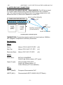
Development of Power Scalable Lasers for Gravitational Wave Interferometry
D. J. Hosken, D. Mudge, C. Hollitt, K. Takeno, P. J. Veitch, M. W. Hamilton and
J. Munch, Prog. Theor. Phys. Supp., 151, 216-220 (May, 2003)
185
Hosken, D.J., Mudge, D., Hollitt, C., Takeno, K., Veitch, P.J., Hamilton, M.W. and
Munch, J. (2003) Development of power scalable lasers for gravitational wave
interferometry.
Progress of Theoretical Physics Supplement, no. 151, pp. 216-220
NOTE: This publication is included on pages 186-190 in the print
copy of the thesis held in the University of Adelaide Library.
It is also available online to authorised users at:
http://dx.doi.org/10.1143/PTPS.151.216
A.2. PUBLICATIONS ARISING AS A RESULT OF THIS THESIS
191
A.2
Publications arising as a result of this thesis
A.2.1
Compensation of Strong Thermal Lensing in HighOptical-Power Cavities
C. Zhao, J. Degallaix, L. Ju, Y. Fan, D. G. Blair, B. J. J. Slagmolen, M. B. Gray,
C.M. Mow Lowry, D. E. McClelland, D. J. Hosken, D. Mudge, A. Brooks, J. Munch,
P. J. Veitch, M. A. Barton and G. Billingsley, Phys. Rev. Lett., 96, 231101(4), (Jun.,
2006)
C. Zhao, J. Degallaix, L. Ju, Y. Fan, D. G. Blair, B. J. Slagmolen, M. B. Gray, C. M.
Lowry, D. E. McClelland, D. J. Hosken, D. Mudge, A. Brooks, J. Munch, P. J.
Veitch, M. A. Barton, and G. Billingsley (2006) Compensation of Strong Thermal
Lensing in High-Optical-Power Cavities
Physical Review Letters, v. 96 (23) , pp. 231101-1 - 231101-4, June 2006
NOTE: This publication is included on pages 192-195 in the print
copy of the thesis held in the University of Adelaide Library.
It is also available online to authorised users at:
http://dx.doi.org/10.1103/PhysRevLett.96.231101
196
A.2.2
APPENDIX A. PUBLICATIONS
Gingin High Optical Power Test Facility
C. Zhao, D.G. Blair, P. Barrigo, J. Degallaix, J-C Dumas, Y. Fan, S. Gras, L. Ju,
B. Lee, S. Schediwy, Z. Yan, D.E. McClelland, S.M. Scott, M.B. Gray, A.C. Searle,
S. Gossler, B.J.J. Slagmolen, J. Dickson, K. McKenzie, C. Mow-Lowry, A. Moylan,
D. Rabeling, J. Cumpston, K. Wette, J. Munch, P.J. Veitch, D. Mudge, A. Brooks,
and D. Hosken, J. Phys.: Conf. Ser., 32, 368-373, (2006)
A.2. PUBLICATIONS ARISING AS A RESULT OF THIS THESIS
A.2.3
197
Observation of three-mode parametric interactions in
long optical cavities
C. Zhao, L. Ju, Y. Fan, S. Gras, B. J. J. Slagmolen, H. Miao, P. Barriga, D. G.
Blair, D. J. Hosken, A. F. Brooks, P. J. Veitch, D. Mudge and J. Munch, Phys. Rev.
A, 78, 023807(6), (Aug., 2008)
APPENDIX A. PUBLICATIONS
198
A.2.4
The Science benets and Preliminary Design of the
Southern hemisphere Gravitational Wave Detector
AIGO
D. G. Blair, P. Barriga, A. F. Brooks, P. Charlton, D. Coward, J-C. Dumas, Y. Fan,
D. Galloway, S. Gras, D. J. Hosken, E. Howell, S. Hughes, L. Ju1, D. E. McClelland,
A. Melatos, H. Miao, J. Munch, S. M. Scott, B. J. J. Slagmolen, P. J. Veitch, L. Wen,
J. K. Webb, A. Wolley, Z. Yan and C. Zhao, J. Phys.: Conf. Ser., 122, 012001(6),
(2008)
A.2. PUBLICATIONS ARISING AS A RESULT OF THIS THESIS
199
APPENDIX A. PUBLICATIONS
200
A.2.5
Observation of optical torsional stiness in a high optical power cavity
Y. Fan, L. Merrill, C. Zhao, L. Ju, D.G. Blair, B.J.J. Slagmolen, D. J. Hosken, A.
F. Brooks, P. J. Veitch, D. Mudge, and J. Munch, to be submitted to Appl. Opt.
(2008)
A.2. PUBLICATIONS ARISING AS A RESULT OF THIS THESIS
A.2.6
201
Direct Measurement of Absorption-Induced Wavefront Distortion in Cavities with High Optical Power
Aidan F. Brooks, David Hosken, Jesper Munch, Peter J. Veitch, Zewu Yan, Chunnong Zhao, Yaohui Fan, Ju Li, David Blair, Phil Willems, Bram Slagmolen and
Jerome Degallaix, Appl. Opt., 48, 355-364, (Jan., 2009)
202
APPENDIX A. PUBLICATIONS
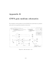
Appendix B
CPFS gain medium schematics
The schematics in this appendix are of the Nd:YAG laser crystals that were produced
and used for the experiments described in this thesis.
Figure B.1: Slab schematic 1 of 3.
203
204
APPENDIX B. CPFS GAIN MEDIUM SCHEMATICS
Figure B.2: Slab schematic 2 of 3.
Figure B.3: Slab schematic 3 of 3.
Appendix C
Laser diode pump module
properties
The pump laser diode arrays used on the nal 10 W slave lasers were purchased
from Cutting Edge Optronics (CEO), with the specications and performance of
these arrays found in this appendix.
C.1
Specications and tolerances
Specications for the Cs double laser diode packages.
• Height tolerance: ? ±50 m (in fast axis)
• 2 × 34 W lensed 1-bar laser diode arrays
• Rated at 22 W at 35 o C heatsink for each bar
• 2 3 mm gap between bars, total emitting length 23 mm
• 45o cut from the front corner of the package. 5 mm in from either side on the
left when looking from the emission side
• 1-bar diode arrays to be connected electrically in series
• Diode arrays collimated in both near eld (rst 50 mm from emitters) and in
the far eld
205
APPENDIX C. LASER DIODE PUMP MODULE PROPERTIES
206
• Collimation parallel to the laser diode package base
• Symmetric intensity lobe of both stripes in the fast-axis direction
Specications for each array used in the Cs double package were:
• Beam divergence of the lensed bar: 1 × 10o (with fast axis lensing)
• Spectral Width : 1=9 nm
• Slope Eciency : 0=9 W/A
• Total Output Power : 34 W
• Maximum Operating Current : 55 A
• Wavelength : 808±2 nm (at the rated output power and heatsink temperature
for the Cs double package : 22 W at 35 o C heatsink temperature)
• The centre wavelengths of each of the stripes are to be matched and the smiles
minimised
• Polarisation : TM
The tolerances required for the manufacture and collimation of the 1-bar laser
diode arrays are shown in Figure C.1. This shows that the collimated output from
each of the laser diode arrays was required to be at the same height and parallel
to the package base, so that both arrays would pump the same plane within the
Nd:YAG slab.
C.2
Custom package schematic
A schematic of the CEO Cs double laser diode package which was used on the nal
10 W slave lasers is shown in Figure C.2.
C.2. CUSTOM PACKAGE SCHEMATIC
207
Figure C.1: Diagram of the tolerances required for the collimation of the laser diode
arrays.
208
APPENDIX C. LASER DIODE PUMP MODULE PROPERTIES
Figure C.2: Schematic of the CEO Cs double package which was used on the nal
10 W lasers.
C.3. CUSTOM PACKAGE PERFORMANCE
C.3
209
Custom package performance
The two double laser diode array packages that were purchased from CEO had serial
numbers 17817 and 17820, and have been referred to as package A and package B
respectively throughout this thesis. Performance specications (supplied by CEO)
for these packages are shown in Figures C.3 and C.4.
210
APPENDIX C. LASER DIODE PUMP MODULE PROPERTIES
Figure C.3: Performance of laser diode array package A.
C.3. CUSTOM PACKAGE PERFORMANCE
Figure C.4: Performance of laser diode array package B.
211
212
APPENDIX C. LASER DIODE PUMP MODULE PROPERTIES
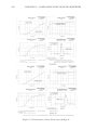
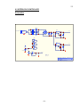
Appendix D
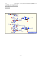
Temperature stabilisation circuit
diagrams
Circuit diagrams used during the course of this work together with descriptions
of the methods used for temperature control are found in this appendix. Unless
otherwise stated, all resistor values are in ohms.
D.1
Laser diode temperature stabilisation
The circuit diagram for laser diode cooling and temperature stabilisation is shown
in Figure D.1. This circuit consists of an error signal stage, pre-amp gain stage
and a power op-amp output stage. The pre-amp stage incorporates a PID stage
followed by a summing op-amp. An instrumentation amplier with a gain of twenty
one precedes the pre-amp stage, the output of which is buered by a power op-amp
output stage with a gain of ve.
Initial and intermediate 10 W laser heads used a single, independent temperature
servo and a single TEC (Melcor CP2-127-06L) to stabilise each laser diode array.
The TEC hotside was bolted to a copper heatsink, initially using water cooling for
ecient heat removal. The intermediate laser used this copper heatsink attached to
another air-cooled aluminium heatsink.
The nal 10 W laser uses a single, temperature stabilised copper block on which
the pump laser diode array is mounted. A single feedback servo independently drives
213
2
1
LM399
3
4
70K
-15V
+15V
1
4
INTEGRATION
AD705
7
-15V
2
3
+15V
1M6
3.9nF
50K
DIFFERENTIATI ON
AD705
6
1M
10K
-15V
2
3
+15V
220nF
2K
SUMMING AMP
AD705
6
-15V
10K
Rg
+
+
4700uF
4700uF
+
1K
2
3
MR752
MR752
MR752
MR752
OUTPUT STAGE
LM12CL
6
5K
V- V+
4700uF
4700uF
+
1K
5
1
4
5
1
4
Figure D.1: Schematic of the laser diode temperature feedback servo.
+/- 16.5V (DC under load)
I= 10A
0.1nF
10μH
0.1 ohm (5W)
10μH
0.1 ohm (5W)
ERROR SIGNAL
OUTPUT STAGE
LM12CL
6
5K
V- V+
V= 28V (AC Bridge)
1K
1K
2
3
Nominal: 2.47K
(measured)
AD620
6
INSTRUMENTATION AMP
Rg = 49.4K/(G-1)
OR G = (49.4K/Rg) + 1
2
3
+15V
5
2M
5
Net feedback: 1.965M (meas)
Nominal: 365K (meas)
-15V
7
820nF
1M3
2
14K7
7
4
27K
1M
6
10K
820nF
820nF
5
470K
1
4
3
1uF
20K
Net feedback: 371K (meas)
Nominal: 207K (meas)
PROPORTIONAL
AD705
6
200K
5
+15V
7
-15V
2
3
+15V
PRECISION
100K
1
4
75K
50K
75K
THERMISTOR (NTC)
100K
7
8
70K
170K
8K
+7V
5
4
Net input: 1.288M (meas)
Nominal: 284K (meas)
Precision Ref .
ANOD
H+
CATH
H-
TEC B
TEC A
0.1nF
Output Mon.
DL serial #17820 on TAMA laser
0.1nF
Output Mon.
214 APPENDIX D. TEMPERATURE STABILISATION CIRCUIT DIAGRAMS
D.2. SLAB TEMPERATURE STABILISATION
215
two TECs (Melcor UT15-12-40-F2-T2-RTV), located side-by-side. Here, the TEC
hot side is cooled by the integrated air-cooled heatsink.
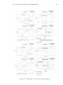
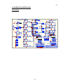
D.2
Slab temperature stabilisation
Slab cooling and temperature stabilisation requires the use of two feedback servos,
with circuit diagrams for the top and bottom servos shown in Figures D.2 and D.3
respectively. Each of these circuits consists of an error signal stage, pre-amp gain
stage and a power op-amp output stage. The pre-amp stage incorporates a PID
stage followed by a summing op-amp. The bottom servo also incorporates a temperature input stage, which allows feedback to the resonator base for long-term
injection locking. Additionally, instrumentation ampliers precede these pre-amp
stages, with gains of seventeen and twenty eight for the slab top and slab bottom
servos respectively. The output of these are then buered by power op-amp output
stages, each with a gain of ve.
The slab is mounted on a large aluminium block (the resonator base), which itself
is mounted on three TECs (Melcor UT6-7-30-F1-T2-RTV), connected electrically in
series to control the slab bottom temperature. This bottom feedback servo uses a
single thermistor as the temperature sensor, located immediately below the slab.
The hot side of the TECs is cooled by the integrated air-cooled heatsink (details in
Chapter 4).
The slab mounting aluminium block is much smaller than the bottom (resonator
base) block. This top block clamps down on the slab by connecting to the heatsink
using a single TEC (Melcor UT6-12-40-F1-T1-RTV). Thermal isolation between
top and bottom blocks is essential to ensure the only thermal connection between
the blocks is through the slab. This is necessary since slab thermal shorts create
diculties when adjusting thermal servos.
2
1
LM399
ANOD
CATH
H+
H-
3
4
33K
1
4
Figure D.2: Schematic of the slab top temperature feedback servo.
-15V
2
3
+15V
2M5
7
3M
5
27K4
INTEGRATION
AD705
6
39nF
10K
DIFFERENTIATI ON
AD705
6
1M
Net feedback: 2.94M(meas)
Nominal: 551K (meas)
-15V
7
10K
-15V
2
3
+15V
220nF
10K
2
3
+15V
-15V
10K
Rg
SUMMING AMP
4K
+
MR752
MR752
V- V+
4700uF
4700uF
+
1K
0.1nF
0.1 ohm
ERROR SIGNAL
Transformer, 2x0-12V, 6.67A (80VA
per secondary); RS#257-5130
+/- 13.3V (DC under load)
V= 22V (AC Bridge)
1K
2
3
OUTPUT STAGE
LM12CLK
6
1uF
5K
Nominal: 3.02K
(measured)
AD620
6
INSTRUMENTATION AMP
Rg = 49.4K/(G-1)
OR G = (49.4K/Rg) + 1
AD705
5V
6
820nF
820nF
4
820nF
10M
2
20K
7
5
510K
10M
3
1
4
1M
1uF
PRECISION
120K
PRECISION
120K
Net feedback: 125K (meas)
Nominal: 75K (meas)
PROPORTIONAL
AD705
6
200K
THERMISTOR (NTC)
100K
PRECISION
20K
10K
5
+15V
7
-15V
2
3
+15V
+7V
20K
PRECISION
FOLLOWER
1
4
51K
8K
THERMISTOR (NTC)
100K
7
8
33K
-15V
+15V
5
Net input: 10M97 (meas)
Nominal: 970K (meas)
Precision Ref .
TEC
0.1nF
Output Mon.
216 APPENDIX D. TEMPERATURE STABILISATION CIRCUIT DIAGRAMS
5
1
4
5
1
4
2
1
LM399
ANOD
CATH
H+
H-
3
4
120K
5M
4M99
7
-15V
2
3
1
4
500K
1uF
5
+15V
7
-15V
20K
INTEGRATION
AD705
6
PROPORTIONAL
AD705
20K
10K
220nF
7
-15V
2
3
+15V
10K
-15V
4K
+
4
MR752
MR752
V- V+
4700uF
4700uF
+
1K
OUTPUT STAGE
LM12CLK
6
5
5
1
4
5
1
4
Figure D.3: Schematic of the slab bottom temperature feedback servo.
0.1nF
0.1 ohm
ERROR SIGNAL
Transformer, 2x0-15V, 5.33A (80VA
per secondary); RS#257-5146
+/- 16.7V (DC under load)
V= 27.5V (AC Bridge)
1K
2
3
1uF
5K
Nominal: 1.81K
(measured)
10K
Rg
AD620
SUMMING AMP
AD705
7V
6
6
INSTRUMENTATION AMP
1
4
Rg = 49.4K/(G-1)
OR G = (49.4K/Rg) + 1
2
3
+15V
7
6
Net feedback: 2M (meas)
Nominal: 430K (meas)
820nF
820nF
58
2
1M
PRECISION
100K
5
3
+15V
THERMISTOR (NTC)
TEC
10K
2
3
-15V
0.1nF
Output Mon.
10K
TEMPERATUREINPUT
+15V
1
4
75K
50K
75K
100K
N/C
(G=1)
AD620
6
58
1M6
8K
+7V
5
120K
-15V
+15V
7
Net input: 5.26M (meas)
Nominal: 278K (meas)
Precision Ref .
D.2. SLAB TEMPERATURE STABILISATION
217
218 APPENDIX D. TEMPERATURE STABILISATION CIRCUIT DIAGRAMS
D.3
Setting the resonator temperature oset
Setting the resonator temperature oset is easily achieved, and is especially important during resonator alignment (see Chapter 3). Setting of the oset is achieved
by:
1. Turning o all temperature controllers for an extended period of time (overnight
if possible), to allow the slab and top/bottom blocks to reach the same temperature.
2. Disconnecting the resonator TEC controller (slab temperature control) feedback connectors from the laser head, then turning on this TEC controller.
3. Measuring the top error signal, then zeroing this signal by adjusting the temperature oset potentiometer.
This potentiometer setting ensures that both the top and bottom thermistors
measure the same temperature, and allow the temperatures of the top and bottom
blocks to be matched.
Appendix E
Thermal lensing measurement
technique
This appendix describes in detail the thermal lensing measurement technique.
E.1
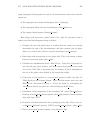
Description of the IDL program
An IDL program was written by Dr Mudge [98] to analyse the interferograms during
thermal lensing analysis. This program was modied for use during the course of
this work, with the program used to analyse interferograms shown in Figure E.1.
This program reads in a fringe pattern (.tif le) and produces sets of cross sectional data by averaging three vertical lines in this image (location of the central line
is determined by the operator, so that it is positioned in the middle of the acquired
image). This data is written to a intensity prole le (v.dat), while les containing
the maxima (m.dat) and the maxima of splines (s.dat) are also produced. This is
in addition to the raw data le (.dat).
E.2
Analysis using fringe peak positions
The analysis was performed using a spreadsheet program, using the acquired raw
data (.dat) and spline data (s.dat) les. These data les were produced for each of
the recorded interferograms that were described in Section 3.8.1, in addition to a
219
220
APPENDIX E. THERMAL LENSING MEASUREMENT TECHNIQUE
Figure E.1: The IDL program used to analyse interferograms.
E.2. ANALYSIS USING FRINGE PEAK POSITIONS
221
single unpumped interferogram for each set of measurements, where these interferograms are
• The unpumped zero fringe interferogram (Zero Unpumped).
• The unpumped tilted reference interferogram (Tilted Reference).
• The pumped interferogram (Pumped Output).
Each fringe peak represents a phase shift of 2, with the procedure used to
analyse the tilted interferograms being as follows:
1. Compare the raw and spline data to conrm that the peaks are correctly
determined for each of the interferograms, and then examine just the spline
data to see if these have all been correctly determined (slab position).
2. Each fringe peak corresponds to a 2 phase shift. This is the change in phase
between consecutive peaks (phase shift).
3. Calculate the magnication factor, MAG Factor. Using Zero Unpumped, locate the slab edge pixel numbers, and then convert from pixels to the actual
size on the CCD. This is determined by the number of pixels multiplied by
the size of the pixels, then divided by the actual slab height.
4. Conversion of slab position to corrected peak positions within the slab, for
Tilted Reference and Pumped Output. These used the known pixel sizes and
MAG Factor, determined in step 2.
These are found by multiplying the
slab position data by the pixel size, then dividing by MAG Factor.
5. Calculation of the magnitude of the introduced tilt, using Tilted Reference.
Plotting corrected peak positions against phase shift produces a linear relationship, with slope TILT.
6. Determine wavefront distortion due to pumping of the slab. This is the corrected phase shift and is given by (TILT*corrected peak positions - phase shift).
7. Plot corrected peak positions against corrected phase shift.
222
APPENDIX E. THERMAL LENSING MEASUREMENT TECHNIQUE
8. This shows a plot with both linear regions and a lens region. Fit a parabola
to the lens region using Equation E.5 (discussed in Section E.3) and extract
the t parameter. This allows the eective focal length to be calculated (as
discussed in Chapter 4).
E.3
Parabolic t to the measured wavefront
The measurement of thermal lensing in the pumped region of the slab requires a
parabola to be tted to the measured wavefront.
As discussed in Chapter 4, beam propagation through the pumped slab is considered as a Gaussian lens duct, with the refractive index n(r,z) given by
μ
¶
1 2 2
q(u> }) = q0 1 u ;
2
where 2 q2 (})
q0 (})
(E.1)
By considering the pumped slab as a lens duct, the optical pathlength seen by a
ray at a distance b(r,z) from the axis (u = 0) varies such that
e(u> }) = } q(u> })
(E.2)
Where o is the total pathlength in the slab, the associated phase shift (compared
to a ray at the axis) seen by propagation through a duct of length o is written as
2
e(u> o) e(0> o)
(o q(u> o) o q(0> o))
= (2)
sureh
sureh
¢
¤
£ ¡
q0 1 12 2 u2 q0 o
= (2)
sureh
2 2
(2) q0 o u
= ,
2sureh
(E.3)
which is in the form of a parabola (| {2 ), with a vertex at (0,0).
A parabola with its axis parallel to the y-axis, vertex at A(x0 ,y0 ) and with the
distance from A to the focus F being d A 0, the general equation is given by [166]
({ {0 )2 = ±4d (| |0 )
(E.4)
E.3. PARABOLIC FIT TO THE MEASURED WAVEFRONT
223
with the ± depending on if the parabola opens up or down.
Fitting to the measured wavefront uses a parabola with a vertex at A(P3 ,P1 ).
By comparing Equations E.3 and E.4 the phase shift is written as
| = S1 ±
(2) q0 o 2 ({ S3 )2
,
2sureh
(E.5)
where
(2) q0 o 2
1
=
4d
2sureh
(E.6)
Once Equation E.5 is tted to the measured wavefront, the parameter is used to
calculate the eective focal length of the lens duct. This is discussed in Section 4.3.4.
224
APPENDIX E. THERMAL LENSING MEASUREMENT TECHNIQUE
Appendix F
Heatsink thermal resistance
calculations
This appendix details the method and formulae used to calculate the heat sink thermal resistance for both natural convection (Section F.1) and forced-air convection
(Section F.2).
F.1
Natural convection
Calculation of the heatsink thermal resistance using natural convection required
both convection and radiation heat dissipation to be considered, together with the
expected average temperature of the heatsink to be known. This allowed the thermal
resistance to be calculated using [119]
vd
1
=
kf Df + ku Du
¸
,
(F.1)
where hf and hu are the convection and radiation heat transfer coecients (each
having units of W/m2 .o C), while Af and Au are the convection and radiation surface
areas (in m2 ).
225
226
F.1.1
APPENDIX F. HEATSINK THERMAL RESISTANCE CALCULATIONS
Radiative area and heat transfer coecient
Radiative heat transfer coecient
Heatsink cooling due to radiation is most useful when the temperature of the
heatsink is considerably higher than the ambient temperature. When performing
calculations involving hu , a temperature dierence between the heatsink and the
surroundings of 20 o C was assumed, for an ambient temperature of 20 o C. This
corresponded to a hu value of approximately 5=68 W/m2 .o C [119] for black anodised
aluminium.
Radiative area
When a heatsink consists of numerous parallel surfaces (ns), the surface area able
to dissipate heat to the surroundings via radiative means is considerably less than
the actual heatsink surface area. For a heatsink with the dimensions shown in
Figure F.1, the radiative area can be approximated by [119]
Du = 2Ki (Z + Oi ) + Z Oi ,
(F.2)
for cases where the n height from the base (Hi ) is over four times the width of the
space between ns (Si ). Here, Li is the vertical length of the heatsink and W is the
overall width of the heatsink.
F.1.2
Conductive area and heat transfer coecient
Conductive heat transfer coecient
For a single isolated vertically mounted surface hf is given by [119]
μ
W
kf = 1=41
Oi
¶1@4
,
(F.3)
where W is the assumed dierence between the heatsink and ambient temperatures.
Equation F.3 can be modied for a parallel surface heatsink by multiplication
by the heat transfer coecient correction factor hf , given by [119]
F.2. FORCED-AIR CONVECTION
227
Figure F.1: Heatsink dimensions, measured in metres.
hf
μ
¶¸
24
1=68I 3
1 exp
,
=
24
1=68I 3
(F.4)
where F is the n spacing parameter, given by
μ
I = 100=7Vi
W
Oi
¶1@4
(F.5)
Conductive area
The conductive area of the heatsink is calculated by determining the total surface
area of the heatsink ns and spacings, while the at, back mounting surface is
excluded since it does not see the ambient conditions.
F.2
Forced-air convection
When cooling a heatsink using forced-air convection, radiation is not a signicant
heat dissipation method. Therefore, Equation F.1 can be simplied and written as
vd =
1
kf Df
where Af is calculated as for natural convection (Section F.1.2).
(F.6)
228
APPENDIX F. HEATSINK THERMAL RESISTANCE CALCULATIONS
Calculation of the conductive heat transfer coecient requires the airow velocity
to be known, allowing hf to be written as [119]
s
kf = 3=86
Y
,
Oi
(F.7)
where V is the linear air velocity (in ms1 ) and Li is the length of the n parallel
to the airow.
Appendix G
Slave laser alignment procedure
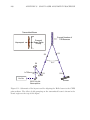
Correct slave laser operation requires careful alignment to the gain region. A carefully aligned HeNe alignment laser is used to align both standing-wave and travellingwave resonators.
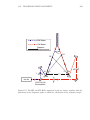
Angles between beams are measured using four thin, sharp alignment spikes
placed in these beams. Measurement of distances between spikes allows calculation
of angles using the cosine rule
d2 = e2 + f2 2ef cos D
G.1
(G.1)
Alignment to the CPFS gain medium
The following procedures are used to align the HeNe laser beam to the CPFS gain
medium.
G.1.1
Horizontal
Horizontal HeNe alignment is achieved with the slab unpumped.
1. Transmit the collimated HeNe beam through the slab. No clipping of this
beam by slab apertures should be observed.
2. Measure the total beam separation angle (ehdp ) between the incident and
transmitted HeNe beams. Alignment spikes placed in this beam (S1, S2, S3
229
APPENDIX G. SLAVE LASER ALIGNMENT PROCEDURE
230
Transmitted Beam
Correct Number of
TIR Bounces
Pumped
Beam Splits
Evenly
Unpumped
S3
S2
Tbeam
S6
f=750mm
S1
S4
He-Ne
50/50 He-Ne
Beamsplitter
Screen
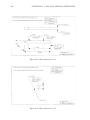
Figure G.1: Schematic of the layout used for aligning the HeNe beam to the CPFS
gain medium. The eect of slab pumping on the transmitted beam is shown in the
boxed region at the top of this gure.
G.1. ALIGNMENT TO THE CPFS GAIN MEDIUM
231
and S4) are used to determine this angle, as shown in Figures G.1 and G.2.
Calculation of 214 and 341 using Equation G.1 allows ehdp to be determined.
3. Adjust the beam separation angle until ehdp = 38=4o is achieved.
4. Once achieved, conrm that there are 10 evenly spaced TIR bounces along the
slab side, between the slab blunt end and the Brewster window shoulder. Fine
adjustment of the HeNe alignment may be required. The HeNe beam must
enter and exit through the Brewster windows, extremely close to the shoulder.
5. Conrm the transmitted beam is not clipping on slab apertures.
6. Repeat steps 2 5 as necessary.
Correct horizontal alignment is achieved when 10 evenly spaced TIR bounces
are observed, with the correct total beam separation angle, and when no clipping of
the transmitted beam is observed.
G.1.2
Vertical
Vertical HeNe alignment requires the slab to be both unpumped and pumped.
1. With the slab unpumped, transmit the HeNe beam through the slab and mark
the position on a screen, as shown in Figure G.1.
2. Pump the slab, observing the position of the transmitted beam on the screen.
The beam will stretch vertically, caused by the dominant vertical thermal lens.
Vertical translation of this beam position, and/or an uneven split indicates
incorrect vertical alignment.
3. Adjust the vertical alignment of the HeNe beam, then compare the unpumped
and pumped transmitted beam positions. Figure G.1 shows the result of correct vertical alignment.
4. Conrm correct horizontal alignment is still achieved. Repeat procedure G.1.1
if required.
5. Repeats steps 1 4 as necessary.
APPENDIX G. SLAVE LASER ALIGNMENT PROCEDURE
232
Correct vertical alignment is achieved when the transmitted HeNe beam splits
evenly and without vertical or horizontal translation.
G.2
Standing-wave alignment
Flat standing-wave mirrors are aligned to the gain medium using the HeNe alignment
beam. An iris placed in the alignment beam, on the input side of the slab, is used
to align mirror back reections. Mirrors need to be perpendicular to this beam.
Once cavity mirrors are aligned, output power optimisation is able to be performed. The HeNe beam can then be realigned to the optimised mirror positions.
The procedure described in Section G.1 is able to conrm the correct bounce solution
is retained after realignment to the standing-wave cavity mirrors.
G.3
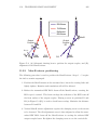
Travelling-wave alignment
Alignment of the travelling-wave resonator uses the alignment beam described in
Section G.1. A second alignment beam is retro aligned to the rst, enabling preservation of the optimised alignment. Alignment beams are referred to as the RW and
FW beams, as shown in Figure G.2.
Initially, the output coupler position and angle needs to be set, before positioning
the Max-R mirror. Positioning of these optics is shown schematically in Figure G.3.
The incidence angle on the output coupler is 10=8o , while that on the Max-R mirror
is 60o .
G.3.1
Output coupler positioning
The following procedure is used to position the output coupler, with the slab remaining unpumped.
1. Position the output coupler at the desired distance from the Brewster window
and lightly clamp.
2. Using the transmitted FW alignment beam through the slab, horizontally
centre this beam on the output coupler. Vertical height should be checked
G.3. TRAVELLING-WAVE ALIGNMENT
233
RW Beam
FW Beam
Distance
Measurements
Tbeam
S3
S2
f
S1
T
T S4
f
He-Ne
50/50 He-Ne
Beamsplitter
f
Figure G.2: The RW and FW HeNe alignment beams are shown, together with the
placement of the alignment spikes to allow the calculation of the separation angle.
234
APPENDIX G. SLAVE LASER ALIGNMENT PROCEDURE
prior to assembly, with appropriate changes being made to the mount when
required. Rotate the output coupler horizontally until an incident angle of
approximately 10=8o is achieved, with the FW beam remaining centred.
3. Setting the correct horizontal output coupler angle uses the back reection of
the RW beam o the output coupler. This is shown in Figure G.3 (A). This
angle is calculated using alignment spikes in the incident and reected RW
beams (S1, S2, S5 and S6). RFedfn should be set to 21=6o .
4. Rotate the output coupler base to keep the FW beam centred, since course
actuator adjustment usually shifts the FW beam o centre.
5. Repeat steps 2 4 until the correct angle for RFedfn is found. Ensure the
output coupler base is clamped securely and that the correct Brewster window
to output coupler distance has been retained. If not, then return to step 1.
6. Inserting the output coupler translates the RW beam. Using adjustable irises
in the FW beam, retro align the RW to the FW beam. Correct RW beam
vertical alignment can be checked by repeating the procedure in Section G.1.2.
7. Vertical tilt of the output coupler needs to be set approximately. The HeNe
alignment beam is usually at through the slab with respect to the optical
table. Setting the height of the RW back reection o the output coupler
to be the same height as the incident RW beam at comparable distances is
usually sucient. However, if the transmitted RW beam is seen to slope down
slightly, then the RW reection o the output coupler should slope up slightly
over a comparable distance, and vice versa.
8. If necessary, repeat steps 6 and 7 after adjusting the vertical tilt.
With the output coupler correctly positioned, the FW alignment beam can be
blocked. The FW beam retains the correct slab alignment, should further output
coupler adjustment be required.
G.3. TRAVELLING-WAVE ALIGNMENT
235
A
B
RW Beam
FW Beam
Reflected
RW Beam
MaxR
Output
Coupler
S5
Output
Coupler
D1
S2
TOCback
S6
S1
RW
Beam
FW
Beam
D2
RW
Beam
Figure G.3: (A) Schematic showing how to position the output coupler, and (B),
alignment of the Max-R mirror.
G.3.2
Max-R mirror positioning
The following procedure is used to position the Max-R mirror. Steps 1 5 require
the slab to remain unpumped.
1. Position the Max-R mount on the resonator base, insert the securing bolts and
lightly tighten. Rotation and translation will still be allowed.
2. Reect the transmitted RW HeNe beam o the Max-R mirror, ensuring the
HeNe spot is centred. This beam overlaps the reection of the RW beam o
the front surface of the output coupler. Placing a screen at positions D1 and
D2 (in Figure G.3 (B)) is used to check beam overlap. Maximise the distance
between D1 and D2.
3. Vertical Max-R mirror adjustment requires the clamping screw on the mount
to be loosened. The tilt adjustment screw is then adjusted to allow the transmitted RW HeNe beam o the Max-R mirror to overlap the reected RW
output coupler beam. Re-tighten the clamping screw to set the vertical tilt.
APPENDIX G. SLAVE LASER ALIGNMENT PROCEDURE
236
4. With the clamping bolts loose, carefully rotate and translate the Max-R mount
horizontally.
5. Repeat steps 24 as necessary. Interference is observed when correctly aligned.
The Max-R base should be bolted down just tight enough to prevent unwanted
movement, but loose enough to allow it to be shifted, if required.
6a. Insert powermeters in the RW and FW beams. Pump the slab at a level just
above laser diode threshold (approximately 1214 amps). Using an IR viewer,
look for lasing. Correct alignment should produce a low threshold with an even
power split in the RW and FW directions.
6b. Conrm the beam is centred on both the Max-R and output couplers. If not,
then return to step 1.
7a. If not lasing, the threshold is high or the output power is not evenly split in
the RW and FW directions, then repeat steps 2 6 before continuing.
7b. If the threshold is low, but the power split is not even, very careful horizontal
adjustment of the Max-R mirror is used to even up the power split. This should
only be performed at a laser diode current level slightly above threshold. Once
power is evened up with mirror spots remaining centred the laser diode current
can be increased once again.
7c. Otherwise, slowly increase the laser diode current while measuring the output
power in both the RW and FW directions. Even power split should be retained.
Continue to increase the laser diode current until the desired pump power is
achieved.
8. Turn down the laser diode current to just above threshold. Pick o a small
fraction of either the RW or FW output beam and align a CCD (or an M2
measuring device).
9. Slowly increase the laser diode current. The vertical mode should be seen to
split evenly about the centre with increased pump power, with an even output
power split. Measure the M2 , if applicable.
G.3. TRAVELLING-WAVE ALIGNMENT
237
10. Tighten the Max-R mirror base bolts. Slight output coupler vertical and
horizontal adjustment can then be performed to improve the mode, if required.
Note 1. On occasions, an additional Max-R mirror mounted on a small adjustable
mount was used to achieve the correct position and alignment. This allowed
minor alignment changes/improvements to be made, while measuring the M2 .
Once the desired M2 and output power was achieved, the nal Max-R mount
could be easily positioned using alignment irises and an additional reected
alignment beam (if necessary).
Note 2. If the vertical mode does not split evenly, or if output decreases with time, then
vertical alignment is incorrect. Vertical adjustment of the output coupler can
often improve this. Max-R mirror vertical adjustment should not be adjusted,
but if required, procedures G.3.1 and G.3.2 should be repeated.
Note 3. Horizontal multimode operation indicates either incorrect slab alignment, or
that the resonator is too short. Procedures G.3.1 and G.3.2 need to be repeated, possibly with an increased Brewster window to output coupler distance. Once horizontal single transverse mode operation is achieved, the vertical mode can be adjusted, if necessary.
Note 4. Single transverse mode operation in the vertical plane requires the vertical
thermal lens to be appropriate for the resonator length. The vertical mode
can be improved by either changing the pump power, or by altering the laser
diode heatsink temperature. This changes the amount of absorbed pump
power, and thus, the vertical thermal lens.
238
APPENDIX G. SLAVE LASER ALIGNMENT PROCEDURE
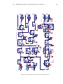
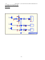
Appendix H
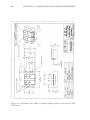
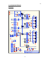
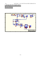
Injection-locking circuit diagrams
Circuit diagrams of the detectors and the feedback servo used for injection-locking
the slave laser are found in this appendix. Unless otherwise stated, all resistor values
are in ohms.
H.1
FW and RW detectors
Chapter 5 describes injection-locking of the 10 W slave laser, which uses the PDH
stabilisation technique. Schematics of the detectors used to are shown in Figure H.1.
H.2
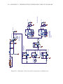
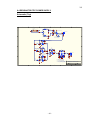
Feedback servo for injection locking
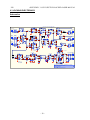
A schematic of the injection-locking electronics is shown in Figure H.2. This servo
contains feedback loops for the three actuators described in Section 5.5.
239
APPENDIX H. INJECTION-LOCKING CIRCUIT DIAGRAMS
240
2.5 mm PLUG
+12 V
50 R
0V
REVERSE DETECTOR
3.3uF
0.1
0.1
PHOTODIODE
G8376-05
REVERSE OUT
50 R
2.5 mm PLUG
+12 V
50 R
0V
FORWARD DETECTOR
3.3uF
0.1
0.1
PHOTODIODE
G8376-05
MIXER
SBL-1
MONITOR
LO IN
L
R
0.1
I
A
4.7 uH
SBL-1
G8376-05
1
3
5
7
2
4
6
8
K
CASE
50 R
BOTTOM VIEW
LO: +7 dBm ~ 500 mV RMS
RF: < 1 dBm ~ 250 mV RMS
1
2
3
4
5
6
7
8
RF
GND
IF
IF
GND
GND
GND
LO
Fc = 1.7 MHz
1.8 nF
IF OUT
4.7 uH
3.6 nF
1.8 nF
DENOTES FERRITE BEAD
Figure H.1: Schematics of the FW and RW detectors which are used for injectionlocking of the 10 W slave laser.
2
3
4
3
1
2
0.1
1
470
R3
9
R4
470
Figure H.2: Schematic of the injection-locking servo.
DIFF
Fc = 15 Hz
Fh = 154 Hz
Fh = 720 kHz
8
470pF
C18
R30 8k45
+12 V
VR1
10 k
R6 5k
82pF
Fc = 388kHz
R29 22k
OP470
U5C
C1
3
2
U1
2 6
3 OP27
8
+
1
OP470
U2A
C16 10pF
C17 T
0.1
R2
56
R1
56
C14 470nF 10
R28 2k2
C15 T
INPUT
HEADER
U7
HF ON
AUX IN
(RP)
DET IN
(RP)
30
ERROR OUT
FP HEADER
(FP)
29
470pF
R32
4k75
C19
R27
10k
6
9
12
13
U7
10
R14 20k
6
DIFF
Fc = 32.2 kHz
Fh = 205 kHz
OP470
U5D
NOTCH FILTER
Fs = 38 kHz
R35
820pF 24k3
12
13
R34 10k
C20 470pF
C23
10k
R33
7
R12 33k
OP470
U2B
C4 22pF
14
10k
VR2
INT
OP470 Fc=10 Hz (sw. open)
Fc=408 Hz
C5 T
14
C3 39nF
U2D
R13 20k
PROP
Fc = 360 kHz
8
7 R11 390k
C21 470pF
C22
T
22pF
R10 20k
OP470
U2C
C6 150pF 5
C7 T
R31 8k45
R9 5k6
R8 10k
R7 10k
C2
470pF
C24
R36
10k
R15
20k
12
13
5
6
U6
14
VR5
10k
OP470
U5B
7
NI
R37 10k
1
R23 10M
OP470
U4A
68uF
C11
NI
I
9
I
3
5
6
OP470
U5A
R19 10k
1
10k
7
5
3
8
C50 6p8
R55 100k
200V
1
U6
7
C55
10pF
R56
330
R50 100
Fc = 230 kHz
8
HD ON
1
OP470
R54 10R
10nF
7
1uF
Z1
-160V
C54
6
6
U4C
200V
10
9
OP470
10nF
+
PA85
-
C53
5
4
U14
C52
2
3
2
U3A
7
R20 10k
OP470
U3B
+160V
Z2
C51 1uF
10k
R21 10k
C10 22pF
6
VR4
R53
1k
R26 10k
OP470
U4B
VR3
R38 10k
8
C13 68pF
C25 68pF
I
OP470
U3C
R18 2k5
R25 10k
10
2
NI
R17 10k
R24
10M t = 340s
3
2
68uF
C12
14
TEMP ON
R22
10M
15
OP470
U3D
R16 2.2k
C9 22pF
NOTE: VR5 on current TAMA PCB is 100k
LOOP GAIN
C8 22pF
R52
51
R51
51k
0.1
0.1
4
3
2
PA85 HEADER
1
2
RP HEADER
1
28
FP HEADER
27
0.1
HD OUT
(RP)
HF MON
(FP)
HF OUT
(RP)
TEMP OUT
(RP)
HD MON
(FP)
HD (TO PIC)
4
RP HEADER
3
DC SUM
H.2. FEEDBACK SERVO FOR INJECTION LOCKING
241
242
APPENDIX H. INJECTION-LOCKING CIRCUIT DIAGRAMS
Appendix I
10 W injection-locked laser manual
As has been described in this thesis, injection-locked 10 W slave lasers were produced
and installed at both TAMA 300 and the ACIGA HPTF. An operating manual was
produced for each of these lasers, and contains circuit diagrams and operational
information.
This appendix contains a copy of the 10 W laser manual for the laser installed at
TAMA 300 (Version 1.1). This document was written and complied by the author
and Dr Damien Mudge. Unless otherwise stated, all resistor values shown in circuit
diagrams are in ohms.
243
244
APPENDIX I. 10 W INJECTION-LOCKED LASER MANUAL
245
10W LASER
(TAMA 300)
Written by David Hosken / Damien Mudge
Version 1.1 (13/12/05)
-1-
246
APPENDIX I. 10 W INJECTION-LOCKED LASER MANUAL
CONTENTS:
1. 10W SLAVE LASER OPERATIONAL SETTINGS
2. 10 W LASER TURN ON/OFF PROCEDURE
3. OPTICAL LAYOUT
4. LASER HEAD AND CONNECTIONS
5. LASER RACK LAYOUT
6. DESCRIPTION OF ELECTRONICS MODULES
6.1
NEWPORT LASER DIODE DRIVER MODEL 5600
6.2
INTERLOCK CONTROLLER
6.3
LOCKING ELECTRONICS
6.4
RESONATOR TEC POWER SUPPLY
6.5
DIODE TEC POWER SUPPLY
6.6
RF / PICOLOG
6.7
SERVO LOCK POWER
7. DETECTORS
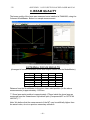
8. MODE MATCHING
9. BEAM QUALITY
-2-
247
GLOSSARY OF TERMS:
•
A/D
: Analogue / Digital
•
ESD
: Electro-Static Discharge
•
FW
: Forward-Wave
•
RW
: Reverse-Wave
•
HD
: High Dynamic Range
•
HF
: High Frequency Range
•
HV
: High Voltage
•
NTC
: Negative Temperature Coefficient
•
PDH
: Pound-Drever-Hall
•
PICOLOG
: Analogue / Digital Converter (Brand Name)
•
PID
: Proportional Integration Differentiation
•
PZT
: Piezoelectric Transducer
•
TEC
: Thermoelectric Cooler
•
n/c
: Not connected
WARNING: The pin connections have been described as accurately as
possible. Check before making any changes!!!!
-3-
248
APPENDIX I. 10 W INJECTION-LOCKED LASER MANUAL
1. 10W SLAVE LASER OPERATIONAL
SETTINGS
NEWPORT LASER DIODE DRIVER:
I0
=
25.50 Amps
LIGHTWAVE NPRO 125/126 SERIES
DC =
1.98 Amps
DT =
21.8 0C
LT =
47.6 0C
T+ =
45.2 0C
Pwr =
223 mW
(Shown on controller)
DIODE TEC POWER SUPPLY:
Set Temp
=
4.38
RESONATOR TEC POWER SUPPLY:
Temp. Offset =
5.53
Set Temp
=
6.50
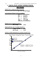
DIODE LASER EMISSION CHARACTERISTICS
Pump Power: Varying Set Temp + Current (DL#1782
Pump Power (Watts)
40
35
SetTemp 5.0
SetTemp 4.5
SetTemp 4.0
Linear Fit of Pump_SetTemp5.0
Linear Fit of Pump_SetTemp4.5
Linear Fit of Pump_SetTemp4.0
SetTemp=5.0
SetTemp=4.5
SetTemp=4.0
30
: PumpPwr= 2.155*I -24.4
: PumpPwr= 2.15 *I -24.52
: PumpPwr= 2.155*I -24.9
25
24
26
28
DL Current, I (Amps)
-4-
30
249
2. 10 W LASER TURN ON/OFF
PROCEDURE
TURN ON
•
Turn the mains plug on (This will power the entire 10W laser rack).
Note: The Diode Laser relies on the earth connection to prevent ESD
•
Reset the SUPPLY FAIL by pressing the button switch on the INTERLOCK
CONTROLLER. This will turn the red LED off.
(Note: In the event of momentary or permanent power failures this LED will
turn on and the laser will not operate. The NEWPORT LASER DIODE
DRIVER will need to be turned off and the turn on procedure needs to be
repeated starting with resetting the SUPPLY FAIL).
•
Clear any faults indicated by the orange FAULT STATUS LEDs on the
INTERLOCK CONTROLLER by pressing the toggle switch down once.
*** If any of the fault LED’s remain on, there is a problem that needs to be
addressed ***
•
Turn on the SERVO LOCK POWER unit (the switch on the left of the
lowest silver unit in the LASER RACK). Each of the small toggle switches
on the right should be turned on (LED’s indicate on). This powers the
AUTO LOCK unit, the FW and RW DETECTORS, cooling FAN, EOM and
the LOCKING ELECTRONICS.
•
Set the DIODE DRIVER ACTIVE, DIODE TEC ACTIVE and RESONATOR
TEC ACTIVE green LED’s by pressing each associated button on the
INTERLOCK CONTROLLER once. This allows the TEC cooling modules
and DIODE LASER DRIVER to be activated.
•
Turn the RESONATOR TEC POWER SUPPLY on.
•
Turn the DIODE TEC POWER SUPPLY on and allow a few minutes for it
to stabilise.
•
Turn the NEWPORT LASER DIODE DRIVER on and turn its key switch to
the on position.
•
Ensure the current reading on the screen reads “0.0A”. Else, turn the
current control knob down to zero.
•
Press the LDD button near the round current control knob on the right of
the unit. This will turn on the green light near the button, indicating the unit
is set to provide power to the Diode Laser.
-5-
250
APPENDIX I. 10 W INJECTION-LOCKED LASER MANUAL
2. 10 W LASER TURN ON/OFF PROCEDURE
•
Turn the current knob to 25.50A slowly. Do not use any more current
(further output power is unlikely to be achieved and misalignment of the
laser could result). Turning the laser up to 25.50A should take several
minutes (ie: do this slowly). The temperatures of the Diode Laser and
SLAB are pre-set.
•
Turn the NPRO on via the key switch. The temperature and current should
be pre-set to suit the laser.
•
Allow several minutes for the laser mode to stabilise.
Locking in manual setup
All instructions below refer to the LOCKING ELECTRONICS – the module
under the INTERLOCK CONTROLLER.
o Ensure the mode switch is set to Manual (MAN).
o Ensure the HD ON switch is set to on (down) – this turns the HD
PZT on.
** Important: The HD ON switch must be in the on position for both
AUTO and MAN. operation. **
o The INT, HF ON and TEMP ON switches should be off (up) initially.
o Turn the OFFSET potentiometer on the LOCKING ELECTRONICS
unit to change the DC OFFSET on the HV supply to drift the PZT
location until the NPRO and 10W slave lasers lock. The reverse
wave will turn off, changing the photodiode output from +V
(unlocked) to zero (locked) (ie: The reverse wave will turn off as all
power is in the forward direction). The RW=0 light should turn on.
Once drift locked, switch the INT switch to on (down) (add in the
integrator). Turn the HF ON switch on (down) (turns the HF PZT
on).
o The ERROR BNC is the PDH error signal.
o Using an oscilloscope (or digital multimeter), measure the HD MON
BNC signal. This needs to be set to zero while locked by changing
the OFFSET potentiometer.
o Turn on the TEMP ON switch (this allows the LOCKING
ELECTRONICS to change the slave temperature very slowly to
keep the DC offset near zero, that is to keep the frequencies of the
NPRO and slave matched).
-6-
251
2. 10 W LASER TURN ON/OFF PROCEDURE
o Note: The time constant of the TEMP ON electronics is several
minutes. This switch must be manually operated and is not
controlled by the AUTO LOCKER.
o The toggle switch can be shifted from MAN to automatic (AUTO).
Note: If in automatic mode, the position of the INT and HF ON are
irrelevant. These switches are bypassed by the AUTO LOCKER.
o The AMPLITUDE sets the overall loop gain and is maximised. If
excess noise appears on the PDH Error signal, decrease the
AMPLITUDE setting to stop oscillations – if the mode matching is
poor the gain needs to be reduced.
-7-
252
APPENDIX I. 10 W INJECTION-LOCKED LASER MANUAL
2. 10 W LASER TURN ON/OFF PROCEDURE
TURN OFF
•
Switch the AUTO LOCKER switch to MAN.
•
Switch the TEMP ON, HF ON and INT switches to their off positions.
•
Reduce the NPRO current to 0A and turn the NPRO off.
•
Turn the current knob on the NEWPORT LASER DIODE DRIVER down to
0A slowly. Turning the Diode Laser current down to 0A should take several
minutes (ie: do this slowly).
•
Press the LDD button on the NEWPORT LASER DIODE DRIVER and the
green led should go off (indicating the Diode Laser is off). Turn the key
switch off and the NEWPORT LASER DIODE DRIVER power switch off.
Allow the laser to cool for several minutes.
•
Turn the RESONATOR TEC POWER SUPPLY off.
•
Turn the DIODE TEC POWER SUPPLY off.
•
Turn each of the small toggle switches on the right of the SERVO LOCK
POWER unit off (LED’s turn off). Turn the SERVO LOCK POWER unit off
(the switch on the left of the lowest silver unit in the LASER RACK).
•
Turn the mains plug off.
(WARNING: always ensure this is plugged in to prevent ESD to the
Diode Laser, even when switched off.)
IMPORTANT: If an interlock shutdown occurs, always ensure the current
control knob on the NEWPORT LASER DIODE DRIVER is turned down to
zero before turning the Diode Laser on again. Do not simply press the LDD
button to reactivate the Diode Laser, otherwise the Diode Laser will be set to
full power as soon as it is turned on, rather than ramped up slowly.
-8-
253
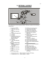
3. OPTICAL LAYOUT
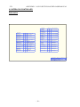
10
9
8
5
7
3
11
26
27
18
19
17
12
32 31
30 16
25
13
4
2
1
14
29
28
6
15
24
20
23
22
21
The optical layout for the injection-locked 10W laser consists of the following
components:
1. Lightwave NPRO
2. YAG beam-steering
mirror
3. YAG beam-steering
mirror
4. 150mm AR-coated lens
5. L/4 plate
6. L/2 plate
7. ElectroOptic Modulator
(EOM), New Focus
Model # 4003M
8. L/2 plate
9. YAG beam-steering
mirror
10. Reverse-wave beam
dump
11. Faraday Isolator (FI),
OFR Model # IO-51064-VHP
12. YAG beam-steering
mirror
13. YAG beam-steering
mirror
14. AR-coated wedge
•
•
15. YAG beam-steering mirror
16. Filter/filter holder (RW)
17. 100mm AR-coated lens
18. YAG beam-steering mirror
19. Reverse-wave detector
(RW Det.)
20. 500mm AR-coated modematching lens
21. YAG beam-steering mirror
22. Periscope
(76.2mm to 130mm)
23. YAG beam-steering mirror
24. YAG beam-steering mirror
25. 200mm AR-coated cylindrical
lens
26. Air-cooled slave laser
27. 200mm AR-coated cylindrical
lens
28. AR-coated wedge
29. 100mm AR-coated lens
30. YAG beam-steering mirror
31. Filter/filter holder (FW)
32. Forward-wave detector/ mixer
(FW Det.)
Components 1-22 : Beam height of 3 inches (76.2mm)
Components 22-32 : Beam height of 130mm
-9-
254
APPENDIX I. 10 W INJECTION-LOCKED LASER MANUAL
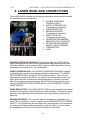
4. LASER HEAD AND CONNECTIONS
The LASER HEAD contains the following components, which are all mounted
on the integrated air-cooled base.
•
•
•
•
•
•
•
•
•
DOUBLE DIODE BAR
PACKAGE (CEO)
DIODE COPPER BLOCK
(Temperature controlled)
PUMP REFLECTOR
RESONATOR BASE
(Temperature controlled)
SLAB TOP BLOCK
(Temperature controlled)
HD RESONATOR MIRROR
MOUNT/OUTPUT COUPLER
HF RESONATOR MIRROR
MOUNT / MAX R MIRROR
THERMISTORS
SLAB
DOUBLE DIODE BAR PACKAGE: Cutting Edge Optronics (CEO) Diode
Laser package has two fast-axis collimated diode bars located side-by-side.
The total available output power is 68W (using two 40W diode bars, lensing
decreases the output power). (See schematic)
DIODE COPPER BLOCK: The DOUBLE DIODE BAR PACKAGE is bolted
(using M4 bolts) onto the temperature controlled copper block. The DIODE
TEC POWER SUPPLY drives two TEC’s under the block. There are two
thermistors mounted in this block, one used for the temperature control set
point, while the other monitors the block temperature to ensure it remains
within the working temperature range. Should this block become too hot or
cold, the INTERLOCK CONTROLLER will turn off the NEWPORT LASER
DIODE DRIVER.
PUMP REFLECTOR: The PUMP REFLECTOR is located parallel and behind
the slab on the opposite side to the Diode Laser package. It reflects any pump
light that is not absorbed on the first pass back into the slab to improve the
efficiency.
RESONATOR BASE: The resonator base is temperature controlled using
three TEC’s connected in series, supplied by the RESONATOR TEC POWER
SUPPLY. Two thermistors are mounted in the resonator base. One thermistor
is used to set the base (slab) temperature, while the other is used to match
the temperature of the top of the slab to the bottom of the slab.
- 10 -
255
4. LASER HEAD AND CONNECTIONS
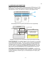
SLAB: This laser uses a coplanar folded zigzag slab (CPFS) that has 10 TIR
bounces/side. It has Brewster angled entrance/exit windows, is side-pumped
and top/bottom cooled. The slab has no coatings. (See diagram below)
PUMP LIGHT REFLECTOR
DIODE
LASER
(40W)
DIODE
LASER
(40W)
Side-pumping the slab using side-by-side diode bars on a single package.
HEATSINK
Nd:YAG SLAB
PUMP REFLECTOR
DOUBLE DIODE
BAR PACKAGE
HEATSINK
HEATSINK
Top/bottom cooling of the slab, side-pumped using the double diode bar package.
SLAB TOP BLOCK: The top block clamps the top of the slab. It is connected
to the LASER BASE via a TEC. The TEC is used to match the temperature of
the top of the slab to the bottom. Two thermistors are mounted in this block,
one directly above the slab for temperature stabilisation, and the other near
the TEC, which is monitored by the INTERLOCK CONTROLLER. If the slab
gets too hot or cold, the RESONATOR TEC POWER SUPPLY will turn off.
HD RESONATOR MIRROR MOUNT/OUTPUT COUPLER: A modified Lees
(Linos) LM2 mount is used to hold the output coupler/PZT. The output coupler
is a 90% reflectance, 5.00mCC optic, on a Piezomechanik PZT stack. (See
details below).
- 11 -
256
APPENDIX I. 10 W INJECTION-LOCKED LASER MANUAL
4. LASER HEAD AND CONNECTIONS
HF RESONATOR MIRROR MOUNT / MAX R MIRROR: The HF mirror mount
is a custom made stainless steel mount with adjustment in the Y-direction
only. The maximum reflectivity (Max R) mirror is a custom coated mirror, with
dimensions 9mm x 6.5mm and is attached to a small PZT.
0
MAX R (60 INCIDENCE)
PUMP LIGHT REFLECTOR
PZT
PZT
DIODE
LASER
(40W)
DIODE
LASER
(40W)
OUTPUT COUPLER
0
(10 INCIDENCE)
OUTPUT
INJECTED BEAM
Travelling-wave resonator layout.
THERMISTORS: Temperature sensors used in the laser head are 100kOhm
NTC (Negative Temperature Coefficient) thermistors.
Part Numbers:
TEC’s:
Diode:
Melcor UT15-12-40-F2-T2-RTV
(x2)
Slab Top:
Melcor UT6-12-40-F1-T1-RTV
(x1)
Resonator Base:
Melcor UT6-7-30-F1-T2-RTV
(x3)
Optics:
MaxR Mirror:
BK7-9-6.5-3-MIRROR
R=99.5% @ 1064nm (theta = 600, p-pol.)
Output Coupler:
PR1-1064-90-0725-5.00CC
R=90% @ 1064nm (theta = 00)
5.00m Concave (0.75 inch diameter)
PZT’s:
HFPZT (MaxR):
Ferroperm Piezoceramics Pz27
HDPZT (90%):
Piezomechanik HPST 1000/25-15/5 (PZT Stack)
- 12 -
257
4. LASER HEAD AND CONNECTORS
Schematic (Double Diode Bar Package)
•
Diode package serial # 17820 used on the 10W Laser for TAMA.
Cooling Fan:
The following fan is located in the base of the LASER RACK and is used for
air-cooling the laser base via a flexible duct.
RS (Australia) Part # 504-928
Description: Slimline axial fan, 120mm frame, 100cft/min, 12V DC
Manufacturer: EBM PAPST
Model:
4312
- 13 -
258
APPENDIX I. 10 W INJECTION-LOCKED LASER MANUAL
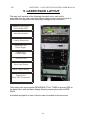
5. LASER RACK LAYOUT
The laser rack consists of the following electronic units; each unit is
removable from the rack. Input and Output cables are secured at the back of
these units to a support frame preventing damage to the connectors.
Newport Laser Diode
Driver Model 5600
Interlock Controller
Locking Electroinics
Resonator TEC
Power Supply
Diode TEC
Power Supply
RF/PICOLOG
Servo Lock Power
Mains Supply Module
Cooling Fan /
Diode TEC Transformer
This locking rack must remain GROUNDED AT ALL TIMES to prevent ESD to
the diode laser, with the Mains Supply Module powering the entire LASER
RACK.
A detailed description of each of these units is included in this document.
- 14 -
259
6. DESCRIPTION OF ELECTRONICS
MODULES
This section describes each of the electronics modules in the LASER RACK,
providing information about the function of the switches, LED’s and
connections, as well as schematics of the electronics.
- 15 -
260
APPENDIX I. 10 W INJECTION-LOCKED LASER MANUAL
6.1 NEWPORT LASER DIODE DRIVER
MODEL 5600
For further information regarding the operation of the NEWPORT LASER
DIODE DRIVER, including computer interfacing etc, please refer to the device
manual.
- 16 -
261
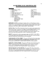
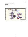
6.2 INTERLOCK CONTROLLER
Front Panel
•
•
•
•
•
•
•
•
EMERGENCY STOP
SUPPLY FAIL
RESET
DIODE DRIVER ACTIVE
DIODE TEC ACTIVE
RESONATOR TEC ACTIVE
FAULT RESET
FAULT STATUS
o DIODE TEMP.
o RESONATOR TEMP.
o BASE TEMP.
o REMOTE
(Push Button)
(LED)
(Push Button)
(LED & RESET Button)
(LED & RESET Button)
(LED & RESET Button)
(Switch)
(LEDs)
EMERGENCY STOP: Activating this button will turn off the Newport Laser
Diode Driver. This method of turning off the laser (pump diode) should only be
used in an emergency, with the usual method for turning off the laser being
described in the 10W LASER TURN ON/OFF PROCEDURE.
SUPPLY FAIL: This LED is illuminated when the supply power to the rack is
turned off and then comes back on again. To reset, press the RESET switch.
This will then allow operation of the INTERLOCK CONTROLLER. The
purpose of this feature is to detect intermittent mains power conditions and
prevent the laser being switched on and off repeatedly and rapidly.
RESET: Resetting this switch is necessary when the SUPPLY FAIL LED is
illuminated. Once reset, the SUPPLY FAIL LED will cease to be illuminated
and the INTERLOCK CONTROLLER can be operated.
DIODE DRIVER ACTIVE (RESET): The green LED will be illuminated when
the RESET button below the LED is pushed once. It will not turn on if a fault
exists, and will require this fault to be rectified before operation. Once
illuminated, the NEWPORT LASER DIODE DRIVER can be operated.
DIODE TEC ACTIVE (RESET): The green LED will be illuminated when the
RESET button below the LED is pushed once. It will not turn on if a fault
exists, and will require this fault to be rectified before operation. Once
illuminated, the DIODE TEC POWER SUPPLY can be operated.
RESONATOR TEC ACTIVE (RESET): The green LED will be illuminated
when the RESET button below the LED is pushed once. It will not turn on if a
fault exists, and will require this fault to be rectified before operation. Once
illuminated, the RESONATOR TEC POWER SUPPLY can be operated.
- 17 -
262
APPENDIX I. 10 W INJECTION-LOCKED LASER MANUAL
6.2 INTERLOCK CONTROLLER
FAULT RESET: To clear any faults indicated by the orange FAULT STATUS
LED’s, press the toggle switch down once. If a fault remains, then there is a
fault that needs to be addressed. Only once all faults have been cleared can
each of the NEWPORT LASER DIODE DRIVER, DIODE TEC POWER
SUPPLY and RESONATOR TEC POWER SUPPLY be operated.
FAULT STATUS LED’s: Indicate that a fault needs to be addressed.
•
•
•
•
DIODE TEMP: Indicates that the temperature of the Diode Laser
copper block is outside its operating temperature range.
Operation range: 12 0C - 45 0C
RESONATOR TEMP: Indicates that the temperature of the resonator
(or slab) is outside its operating temperature range.
Operation range: 12 0C - 45 0C
BASE TEMP: Indicates that the temperature of the air-cooled laser
base is outside its operating range.
Operation range: 12 0C - 50 0C
REMOTE: This indicates that the remote switch has been triggered.
Such a remote trigger could be a Reed switch on a door to an
enclosure or similar.
These faults can only be cleared once the Diode/Resonator/Base are within
their operating temperature range, or once the remote trigger has been reset.
Depending on the fault, the INTERLOCK CONTROLLER makes a decision
about which modules should be shut down. This means that all three units will
not necessarily be shut down when a fault is detected, only those directly
affected.
- 18 -
263
6.2 INTERLOCK CONTROLLER
Rear Panel
•
•
•
Inputs:
o REMOTE
o LASER
Outputs:
o DIODE TEC
o RESONATOR TEC
o DIODE DRIVER
Power/Others:
o DIODE TEMP MON.
o RESONATOR TEMP MON.
o BASE TEMP MON.
o IEC (MAINS IN)
(4-pin plug/socket)
(D9 plug/socket)
(2-pin plug/socket)
(2-pin plug/socket)
(D9 plug/socket)
(BNC)
(BNC)
(BNC)
(3-pin)
REMOTE: This two-pin connector is attached to the INTERLOCK
CONTROLLER and can be connected to a Reed-type switch.
LASER: This connector is attached to the LASER HEAD via a cable and
monitors three thermistors mounted within the LASER HEAD. These signals
are used by the INTERLOCK CONTROLLER to monitor temperatures and
detect faults that may require one or more of the control units to be turned off.
DIODE TEC: The output to the DIODE TEC POWER SUPPLY provides +5V
signal when there is no fault. If there is a fault, the output is 0V and the DIODE
TEC POWER SUPPLY unit will not operate. Therefore, this cable must be
connected for the laser to be operated.
RESONATOR TEC: The output to the RESONATOR TEC POWER SUPPLY
provides +5V signal when there is no fault. If there is a fault, the output is 0V
and the RESONATOR TEC POWER SUPPLY unit will not operate. Therefore,
this cable must be connected for the laser to be operated.
DIODE DRIVER: This output is connected to the NEWPORT LASER DIODE
DRIVER. The NEWPORT LASER DIODE DRIVER provides +5V signal and
tests for continuity between two pins on a D connector on the rear of the unit.
Should it detect an open circuit, the driver is turned off. The INTERLOCK
CONTROLLER uses an optical switch to create an open-circuit should a fault
be detected, thus requiring the driver to be turned off. Therefore, the laser
cannot be operated unless this cable is connected.
DIODE TEMP. MON: BNC output, used to monitor the temperature of the
copper block on which the Diode Laser is mounted. This is usually connected
to the PICOLOG A/D converter, allowing the temperature of the block to be
monitored and logged. The temperature from the thermistor has been
linearised, and the output voltage can be converted to 0C using:
Diode Temp (0C) = DiodeTempMon (V) * 10
- 19 -
264
APPENDIX I. 10 W INJECTION-LOCKED LASER MANUAL
6.2 INTERLOCK CONTROLLER
RESONATOR TEMP MON: BNC output, used to monitor the temperature of
the resonator base (slab). This is usually connected to the PICOLOG A/D
converter, allowing the temperature of the resonator base to be monitored and
logged. The temperature from the thermistor has been linearised, and the
output voltage can be converted to 0C using:
Resonator Temp (0C) = ResonatorTempMon (V) * 10
BASE TEMP MON: BNC output, used to monitor the temperature of the laser
base (heatsink). This is usually connected to the PICOLOG A/D converter,
allowing the temperature of the laser base to be monitored and logged. The
temperature from the thermistor has been linearised, and thus, the output
voltage can be converted to 0C using:
Base Temp (0C) = BaseTempMon (V) * 10
IEC: 100V AC with ground connection.
- 20 -
265
6.2 INTERLOCK CONTROLLER
Plug/Socket Pin connections
Remote 4-pin plug/socket
Pin#1
to reed switch
Pin#2
n/c
Pin#3
n/c
Pin#4
to reed switch
(or bypass shunt between 1 and 4)
Laser D9 plug/socket (using 100kOhm NTC)
Pin#1
shield
Pin#2
diode-laser thermistor
Pin#3
diode-laser thermistor
Pin#4
slab thermistor
Pin#5
slab thermistor
Pin#6
base thermistor
Pin#7
base thermistor
Pin#8
n/c
Pin#9
n/c
Diode TEC 5V Interlock 2-pin plug/socket
Pin#1
Ground
Pin#2
+5V
Resonator TEC 5V Interlock 2-pin plug/socket
Pin#1
Ground
Pin#2
+5V
Diode Driver Interlock D9 plug/socket
Pin#1
connected (used by Newport driver)
Pin#2
connected (used by Newport driver, shield)
Pin#3
n/c
Pin#4
n/c
Pin#5
n/c
Pin#6
n/c
Pin#7
n/c
Pin#8
n/c
Pin#9
n/c
Nominal fuse for Interlock Controller:
- 21 -
100mA, 250V, M205
266
APPENDIX I. 10 W INJECTION-LOCKED LASER MANUAL
6.2 INTERLOCK CONTROLLER
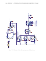
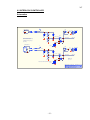
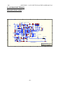
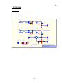
Schematics
TEMPERATURE SENSORS
(MAY BE THERMISTOR OR LM35)
FOUR PAIR SHIELDED CABLE
TEMP SENSOR 1
+5
3
J2
(ON PCB)
23
2
24
DE9
THERMISTOR
0.1
SENSOR 1
(DIODE 1 TEMP)
0.1
TEMP SENSOR 2
+5
0.1
9
25
8
26
LM35
200 R
SENSOR 2
(DIODE 2 TEMP)
0.1
+5
TEMP SENSOR 3
0.1
THERMISTOR
5
19
4
20
SENSOR 3
(SLAB TEMP)
0.1
+5
TEMP SENSOR 4
0.1
THERMISTOR
7
21
6
22
SENSOR 4
(BASE TEMP)
0.1
SHIELD
1
11
2
4 PIN CONNECTOR
SW 1 (WATER)
0.1
1
7
3
0.1
RP5B 1
100k
7
12
13
FAULT 5
(WATER)
DS2A
DISSABLE FAULT 5
9
4 PIN CONNECTOR
+5
8
10
SW 2 (DOOR)
RP5A 1
100k
+5
FAULT 6
(DOOR)
DS2B
DISSABLE FAULT 6
2
14
SWITCHES OPEN FOR FAULT
THE UNIVERSITY OF ADELAIDE - DEPARTMENT OF PHYSIC
DENOTES FERRITE BEAD
OPTICS GROUP - INTERLOCK UNIT
SENSOR CONNECTIONS
30-Nov-2005 C:\USERS\..\SENSORS.SCH
- 22 -
1/9
267
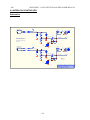
6.2 INTERLOCK CONTROLLER
Schematics
+5
TEMP SENSOR 1
U17B
5
THERMISTOR
2k2
7
V = 0.054T + 0.87
J2
TEMP MON 1
28
6
27
64.9 k
LM324
L
L
65.2 k
300 R
200 R
U17A
V = 0.01T + 0.16 3
1
0.1
14.7 k
100 mV/deg C
TEMP SIG 1
2
TEMPERATURE SENSORS
(MAY BE THERMISTOR OR LM35)
LM324
14.8 k
100 R
1 uF
THERMISTOR: 100 k @ 25 deg C
(RS 151-243)
20 k
T
180 k
L
TEMP SENSOR 2
0.178 V
+5
U17C
10
2k2
8
LM35
200 R
V = 0.1T
J2
TEMP MON 2
30
9
29
64.9 k
LM324
L
L
65.2 k
300 R
200 R
U17D
V = 0.01T 12
14
0.1
14.7 k
100 mV/deg C
TEMP SIG 2
13
LM324
14.8 k
100 R
1 uF
20 k
THIS CIRCUIT SHOWN JUMPERED FOR LM35
T
180 k
LM324
pin 11 = GND
pin 4 = +8 V
L
0.178 V
THE UNIVERSITY OF ADELAIDE - DEPARTMENT OF PHYSIC
OPTICS GROUP - INTERLOCK UNIT
TEMPERATURE SENSING CIRCUITS 1 & 2
30-Nov-2005 C:\USERS\..\TEMP1&2.SCH
- 23 -
2/8
268
APPENDIX I. 10 W INJECTION-LOCKED LASER MANUAL
6.2 INTERLOCK CONTROLLER
Schematics
+5
TEMP SENSOR 3
U19B
5
THERMISTOR
2k2
7
V = 0.054T + 0.87
J2
TEMP MON 3
18
6
17
64.9 k
LM324
L
L
65.2 k
300 R
200 R
U19A
V = 0.01T + 0.16 3
1
0.1
14.7 k
100 mV/deg C
TEMP SIG 3
2
TEMPERATURE SENSORS
(MAY BE THERMISTOR OR LM35)
LM324
14.8 k
100 R
1 uF
THERMISTOR: 100 k @ 25 deg C
(RS 151-243)
20 k
T
180 k
L
0.178 V
+5
TEMP SENSOR 4
U19C
10
THERMISTOR
2k2
8
V = 0.054T + 0.87
J2
TEMP MON 4
16
9
15
64.9 k
LM324
L
L
65.2 k
300 R
200 R
U19D
V = 0.01T + 0.1612
14
0.1
14.7 k
100 mV/deg C
TEMP SIG 4
13
LM324
14.8 k
100 R
1 uF
20 k
T
180 k
LM324
pin 11 = GND
pin 4 = +8 V
L
0.178 V
THE UNIVERSITY OF ADELAIDE - DEPARTMENT OF PHYSIC
OPTICS GROUP - INTERLOCK UNIT
TEMPERATURE SENSING CIRCUITS 3 & 4
30-Nov-2005 C:\USERS\..\TEMP3&4.SCH
- 24 -
3/9
269
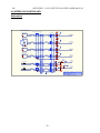
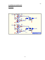
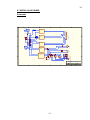
6.2 INTERLOCK CONTROLLER
Schematics
+5
15
RP9B 2
1k
1
TEMP SIG 1
6 RP10F 11
1M
RP7C
100 k
4
U15A
5
2
TOO HOT
4
0.1
LM339
HOT THRESHOLD 1
RP9A 16
1k
1
5k
2
U12B
+5
5 RP10E 12
1M
U12A
1
4
12
6
13
FAULT 1
10
FAULT 2
11
74C02
74C02
74C02
DS1C
RP7D
100 k
3
6
4
+5
5
U15B
U13D
3
1
RP9H 8
1k
9
5
+5
7
TOO COLD
1
DISSABLE FAULT 1
6
RP6C
100 k
1
0.1
LM339
COLD THRESHOLD 1
RP9C14
1k
3
+5
5k
+5
11
RP9F 6
1k
1
TEMP SIG 2
7 RP10G 10
1M
RP7B
100 k
3
U15C
9
14
TOO HOT
8
0.1
LM339
HOT THRESHOLD 2
RP9G 10
1k
7
RP9D 4
1k
8
11
U12C
+5
8 RP10H 9
1M
U12D
13
10
9
9
8
74C02
74C02
74C02
DS1D
RP7A
100 k
4
5
5
+5
2
U15D
U13C
12
1
13
5k
+5
11
TOO COLD
13
DISSABLE FAULT 2
10
RP6D
100 k
1
0.1
LM339
COLD THRESHOLD 2
5
RP9E 12
1k
5k
+5
LM339
pin 12 = GND
pin 3 = +8 V
THE UNIVERSITY OF ADELAIDE - DEPARTMENT OF PHYSIC
OPTICS GROUP - INTERLOCK UNIT
TEMPERATURE COMPARITORS 1 & 2
30-Nov-2005 C:\USERS\..\COMP1&2.SCH
- 25 -
4/9
270
APPENDIX I. 10 W INJECTION-LOCKED LASER MANUAL
6.2 INTERLOCK CONTROLLER
Schematics
+5
4 RP11D 13
1k
1
TEMP SIG 3
1 RP10A 16
1M
RP8D
100 k
5
U16A
5
2
TOO HOT
4
0.1
LM339
HOT THRESHOLD 3
16 RP11A 1
1k
5k
2
U14B
+5
2 RP10B 15
1M
U14A
1
4
2
6
1
FAULT 3
4
FAULT 4
3
74C02
74C02
74C02
DS1B
RP8C
100 k
2
7
3
+5
4
U16B
U13A
3
1
6 RP11F 11
1k
5
+5
7
TOO COLD
1
DISSABLE FAULT 3
6
RP6B
100 k
1
0.1
LM339
COLD THRESHOLD 3
14 RP11C 3
1k
+5
5k
+5
8 RP11H 9
1k
1
TEMP SIG 3
4 RP10D 13
1M
RP8B
100 k
3
U16C
9
14
TOO HOT
8
0.1
LM339
HOT THRESHOLD 4
10 RP11G 7
1k
5k
11
U14C
+5
3 RP10C 14
1M
U14D
13
10
5
9
6
74C02
74C02
74C02
DS1A
RP8A
100 k
1
8
2
+5
2
U16D
U13B
12
1
2 RP11B 15
1k
8
+5
11
13
TOO COLD
DISSABLE FAULT 4
10
RP6A
100 k
1
0.1
LM339
COLD THRESHOLD 4
12 RP11E 5
1k
5k
+5
LM339
pin 12 = GND
pin 3 = +8 V
THE UNIVERSITY OF ADELAIDE - DEPARTMENT OF PHYSIC
OPTICS GROUP - INTERLOCK UNIT
TEMPERATURE COMPARITORS 3 & 4
30-Nov-2005 C:\USERS\..\COMP3&4.SCH
- 26 -
5/9
271
6.2 INTERLOCK CONTROLLER
Schematics
5
D
Q
1
1
U7A
CD4013
Q
2
LTCHFLT 1
13
17
J1
EMERGENCY STOP
1
U5
15
8
FAULT RESET
8 S
9
+5
D
Q
(E+1+2+3+4+5+6)4 U6B
6
5
74C30
74C32
13
U7B
CD4013
U4B
5
4
6
74C02
2
1
FAULT 3
D
Q
8 S
Q
2
LTCHFLT 3
12
PWR FAIL
1
11
(3+4)
12
9
5
+5
RP4D 5
100k
3
D
74C32
74C20
13
U8B
CD4013
+5
12
12
6
U1
74HC540
9
Q1
Q2
Q318
Q417
Q516
Q615
Q714
Q813
12
11
10
J1
Q
U9A
CD4013
74C32
R
Q
2
RP1
470 R
LTCHFLT 5
FAULT 6
11
U9D
9
13
8 S
74C02
D
12
11
R
74C02
Q 13
U9B
CD4013
Q 12
23
14
16
18
20
22
ENABLE 3
10
9
ENABLE 2
16
15
14
13
12
11
10
9
ENABLE 1
4
8
3
U9C
RP2
470 R
1
2
3
4
5
6
7
8
2
1
16
15
14
13
12
11
10
9
D
Q1
Q2
Q318
Q417
Q516
Q615
Q714
Q813
12
11
6 S
5
3
1
2
3
4
5
6
7
8
FAULT 5
1
U2
74HC540
LTCHFLT 4
2
3 D1
4 D2
5 D3
6 D4
7 D5
8 D6
9 D7
D8
1
19 E1
E2
10
Q
11
U6A
ENBL 3
1
Q
U11A
CD4013
2
Q
2
3 D1
4 D2
5 D3
6 D4
7 D5
8 D6
9 D7
D8
1
19 E1
E2
Q
11
8
+5
D
R
PWR FAIL CLEAR
13 U6D
U3B
PWR FAIL
8 S
10
J1
RP4C 4
100k
74C32
FAULT 4
9
1
10
74C20
4
R
Q
8
8
10
9
U11B
4013
11
13
12
ENBL 2
13
Q
U10B
CD4013
12
Q
R
PWR FAIL
4
13
R
Q
11
9 U6C
(1+2+3+4)
D
1
U8A
CD4013
3
9
6 S
6 S
5
D
U3A
6
74C02
9
Q
LTCHFLT 2
10
4 RESET
1
3
+5
1 RP4A 2
100k
PWR FAIL
12
R
5
U4A
10
RST 2
R
DS1813
11
ENBL 1
1
Q
U10A
CD4013
2
Q
D
8 S
4
3
2
1
FAULT 2
9
5
+5
RP4B 3
100k
3
4
12
11
6
5
R
9
+5
RP3D 5
100k
4
1
R
3
J1
+5
RP3C 4
100k
6 S
6 S
FAULT 1
5
2
4
1
3
J1
24
J1
ENABLE AND
PWR FAIL LEDS
E1
E2
E3
PF
THE UNIVERSITY OF ADELAIDE - DEPARTMENT OF PHYSIC
LTCHFLT 6
10
FAULT LEDS
F2
F1
F4
F3
F6
F5
OPTICS GROUP - INTERLOCK UNIT
FAULT LOGIC
30-Nov-2005 C:\USERS\..\LOGIC.SCH
- 27 -
6/9
272
APPENDIX I. 10 W INJECTION-LOCKED LASER MANUAL
6.2 INTERLOCK CONTROLLER
Schematics
+5
220 R
+5
DIODE DRIVER
+5
0.1
2N3642
ENBL 1
L1
10 k
1
470 R
6
2
J2
DE9
5
6
1
1
4
8
2
2
220 R
4N25 (FCD810)
SHIELD
L2
0.1
10 k
+5
2N3642
ENBL 2
SSR (DIODE TEC)
2 PIN CONNECTOR
4
0.1
CONTROL INPUT
3
SHIELD
+5
2N3642
ENBL 3
SSR (SLAB TEC)
2 PIN CONNECTOR
2
0.1
CONTROL INPUT
1
SHIELD
DENOTES FERRITE BEAD
THE UNIVERSITY OF ADELAIDE - DEPARTMENT OF PHYSIC
OPTICS GROUP - INTERLOCK UNIT
ENABLE CIRCUITS
30-Nov-2005 C:\USERS\..\ENABLE.SCH
- 28 -
7/9
273
6.2 INTERLOCK CONTROLLER
Schematics
J3
(ON PCB)
L
110 VAC MAINS E
IN
+5 V
OUT
ADJ
N
LM317
IEC CONNECTOR
LINE FILTER
AND FUSE
220 R
0.1
10 uF
1k
U18B
5
7
6
LM324
U18C
10
LM317
8
9
IN
LM324
U18D
220 R
0.1
12
6.8 k
+8 V
OUT
ADJ
+5
10 uF
14
13
2k
LM324
1.5 k
LM385-1.2
500 R
U18A
3
1
0.178 V
2
1k
LM324
LM324
pin 11 = GND
pin 4 = +8 V
THE UNIVERSITY OF ADELAIDE - DEPARTMENT OF PHYSIC
OPTICS GROUP - INTERLOCK UNIT
POWER SUPPLIES
30-Nov-2005 C:\USERS\..\POWER.SCH
- 29 -
8/9
274
APPENDIX I. 10 W INJECTION-LOCKED LASER MANUAL
6.2 INTERLOCK CONTROLLER
Schematics
TEMP MON 2
(DIODE 2)
30 29
GND FOR TEMP MON 2
TEMP MON 1
(DIODE 1)
28 27
GND FOR TEMP MON 1
TEMP SENSOR 2
(DIODE 2)
26 25
+5 V FOR TEMP SENSOR 2
FAULT 5 LED
(WATER)
24 23
GND FOR FAULT LEDS
TEMP SENSOR 1
(DIODE 1)
24 23
+5 V FOR TEMP SENSOR 1
FAULT 6 LED
(DOOR / REMOTE)
22 21
GND (NOT USED)
TEMP SENSOR 4
(BASE)
22 21
+5 V FOR TEMP SENSOR 4
FAULT 3 LED
(SLAB TEMPERATURE)
20 19
GND (NOT USED)
TEMP SENSOR 3
(SLAB)
20 19
+5 V FOR TEMP SENSOR 3
FAULT 4 LED
(BASE TEMPERATURE)
18 17
EMERGENCY STOP SWITCH
TEMP MON 3
(SLAB)
18 17
GND FOR TEMP MON 3
FAULT 1 LED
(DIODE 1 TEMPERATURE)
16 15
FAULT RESET SWITCH
TEMP MON 4
(BASE)
16 15
GND FOR TEMP MON 4
FAULT 2 LED
(DIODE 2 TEMPERATURE)
14 13
+5 V FOR
EMERGENCY STOP SWITCH
SHIELD FOR FAULT 6
14 13
GND FOR FAULT 6
FAULT 6
(DOOR)
ENABLE 2 SWITCH
(DIODE TEC)
12 11
+5 V FOR
PWR FAIL CLEAR SWITCH
12 11
SHIELD FOR
TEMP SENSORS
ENABLE 1 SWITCH
(DIODE DRIVER)
10 9
+5 V FOR ENABLE AND
FAULT RESET SWITCHES
FAULT 5
(WATER)
10 9
GND FOR FAULT 5
PWR FAIL CLEAR SWITCH
8
7
GND (NOT USED)
DIODE DRIVER -
8
7
SHIELD FOR FAULT 5
ENABLE 3 SWITCH
(SLAB TEC)
6
5
GND FOR ENABLE AND
PWR FAIL LEDS
DIODE DRIVER +
6
5
GND (NOT USED)
ENABLE 2 LED
(DIODE TEC)
4
3
PWR FAIL LED
DIODE TEC SSR+
4
3
DIODE TEC SSR-
ENABLE 1 LED
(DIODE DRIVER)
2
1
ENABLE 3 LED
(SLAB TEC)
SLAB TEC SSR+
2
1
SLAB TEC SSR-
J1
J2
THE UNIVERSITY OF ADELAIDE - DEPARTMENT OF PHYSIC
OPTICS GROUP - INTERLOCK UNIT
PIN ASSIGNMENTS FOR HEADERS J1 AND J2
30-Nov-2005 C:\USERS\..\J1&J2.SCH
- 30 -
9/9
275
6.3 LOCKING ELECTRONICS
Front Panel
Locking:
• AUTO. / MAN.
• HD ON
• INT.
• HF ON
• TEMP. ON
• HF GAIN
• DIFF GAIN
• LOOP GAIN
• TEMP. GAIN
(Switch)
(Switch)
(Switch)
(Switch)
(Switch)
(Trim pot – 10 turn)
(Trim pot – 10 turn)
(Trim pot – 10 turn)
(Trim pot – 10 turn)
Auto Locker:
• SCAN
• NO RW = 0
• RW = 0
• LOOP LOCKED
• RESET
(Yellow LED)
(Red LED)
(Green LED)
(Green LED)
(Push button)
Monitors:
• ERROR
• HD MON.
• HF MON.
(BNC)
(BNC)
(BNC)
HD PZT High Voltage Amplifier
• AMPLITUDE
• OFFSET
• LC DISPLAY
(SQV 1/1000)
(Knob)
(Knob)
Locking:
AUTO. / MAN: This switch selects the method of locking. When the switch is
in the manual position, locking can be achieved by using the SQV 1/1000
OFFSET knob to adjust the DC level to the HD PZT and following the manual
locking procedure. With this switch in the automatic position, the laser can
automatically acquire lock and close the appropriate switches. The INT and
HF ON switches can be in either position when using the Automatic locking
mode.
HD ON: The switch turns on the feedback to the High Dynamic (HD) range
PZT. When the switch is in the up position, there is no feedback from the
locking circuit to the HD PZT high voltage amplifier. Turning this switch to the
down (or on) position will allow feedback to the HD PZT. This switch must
remain in the down position for locking in both manual and automatic modes.
- 31 -
276
APPENDIX I. 10 W INJECTION-LOCKED LASER MANUAL
6.3 LOCKING ELECTRONICS
INT: When this switch is in the down (or on) position, the integrator is
introduced into the HD PZT feedback circuit.
HF ON: When this switch is in the down (or on) position, the High Frequency
(HF) PZT is engaged.
TEMP. ON: This switch provides slow feedback to the resonator temperature,
using the RESONATOR TEC POWER SUPPLY. The temperature feedback
increases the dynamic range of the locking by allowing the circuit to
compensate for slow frequency drifts between the master and slave lasers.
This switch must be in the down position to use this feature, as the
temperature feedback is not controlled by the AUTO LOCKER.
HF GAIN: Trimpot used to adjust the High Frequency (HF) loop gain.
Clockwise adjustment increases the HF loop gain. This gain has been pre-set.
DIFF GAIN: Trimpot used to adjust the differential gain of the High Dynamic
(HD) range loop. Clockwise adjustment increases the differential gain. This
gain has been pre-set.
LOOP GAIN: Trimpot used to adjust the overall gain of the HD loop.
Clockwise adjustment increases the HD loop gain. This gain has been pre-set.
TEMP. GAIN: Trimpot used to adjust the gain of the temperature feedback to
the RESONATOR TEC POWER SUPPLY. Clockwise adjustment increases
the gain. This gain has been pre-set.
Auto Locker:
SCAN: When the yellow LED is illuminated, the auto-locker is scanning the
HD PZT by applying a ramp voltage. It will continue to scan until the reversewave is suppressed. It will scan with increasing voltage over a region of
approximately 200V and then scan back down.
NO RW = 0: If this red LED is illuminated, it indicates that the auto-locker has
completed one full scan, and has failed to find a RW=0 event. The auto-locker
will however continue to scan, attempting to find a lock. If the NO RW=0 LED
remains illuminated, the operator may need to intervene and explore if there is
a misalignment or some other problem.
RW = 0: Illumination of this green LED indicates that the auto-locker has
found a HD PZT voltage where the reverse-wave is suppressed, and it is no
longer scanning. If this is illuminated, then the reverse-wave is suppressed.
This can be used to indicate when RW=0 when manual locking also. If it is not
illuminated, then the reverse-wave is not suppressed and the slave laser is
running bi-directional.
- 32 -
277
6.3 LOCKING ELECTRONICS
LOOP LOCKED: When the green LED is illuminated, the auto-locker has
found RW = 0 and has switched the integrator into the circuit, the HF PZT and
has reduced the DC offset at the HD MON port to be close to zero. Once this
has been achieved, the LED will be illuminated. This implies that the laser has
been successfully locked using the auto-locker.
RESET: Pressing this button will reset the auto-locker to its initial state. Once
pressed, the operator is able to switch from manual to automatic mode without
the laser losing lock.
Monitors:
ERROR: BNC output allows the user to connect to an oscilloscope and
monitor the PDH error signal.
HD MON: BNC output allows the user to connect to an oscilloscope and
monitor the signal from the locking card for the HD PZT loop. The buffered
signal is identical to the signal to the SQV 1/1000 high voltage amplifier
(inbuilt). The DC level should be kept close to zero, to prevent the high
voltage amplifier from running out of dynamic range.
HF MON: BNC output allows the user to monitor the signal applied to the High
Frequency (HF) PZT. Note: a voltage divider (1:1000) on the output is used.
HD PZT High Voltage Amplifier (SQV 1/1000)
The High Voltage Amplifier is a PiezoMechanik SQV 1/1000 Single Channel
Amplifier +1000V Output.
(***Information from Piezomechanik Datasheet: Amplifiers, D/A Converters,
Electronic HV-Switches for Piezonactuators***)
Input
Input:
Input resistance:
Input connector:
+/- 5V (or +/- 10V, depending on Amplitude Potentiometer
Setting. See below)
10kOhm
BNC
Output
Voltage range:
0V to +1000V
Max. peak current/average current: approx. 10mA
Gain:
200
Connector:
LEMOSA OS.250
Noise:
approx. 5mVpp with capacitive load (actuator)
Display:
LCD, 3 digits
Dimensions:
WxDxH 165x210x70mm
Weight:
approx.1.7kg
- 33 -
278
APPENDIX I. 10 W INJECTION-LOCKED LASER MANUAL
6.3 LOCKING ELECTRONICS
AMPLITUDE: This single turn potentiometer can be used to adapt the input
signal to the working range of the amplifier. It makes it possible to use signal
levels of 5V as well as 10V (see SQV 1/1000 specifications). The
potentiometer determines the overall gain for the HD PZT feedback loop.
OFFSET: The SQV 1/1000 HV amplifier uses an offset potentiometer to
manually set the DC output voltage over the full operating range. Thus, the
amplifier can be used as an adjustable voltage supply when no external signal
is applied. When an external signal is applied, the “Offset” voltage is
superimposed automatically.
The potentiometer is used to change the DC voltage to the HD PZT to achieve
locking when in the manual locking mode. When operating in the automatic
mode, the DC level should initially be set to approximately 400V.
LC DISPLAY: 3-digit display indicates the approximate DC voltage to the HD
PZT.
- 34 -
279
6.3 LOCKING ELECTRONICS
Rear Panel
•
•
•
Inputs:
o RW IN
o AUX IN
o DET IN
Outputs:
o HV OUT
o TEMP. OUT
o HF OUT
o PIC STATUS
Power/Others:
o PIC PROGRAMMING JACK
o DC POWER
o LOGIC 5V
o 100V (Fixed IEC female cable)
(BNC)
(BNC)
(BNC)
(LEMO)
(BNC)
(BNC)
(BNC)
(D15)
(D9)
RW IN: This signal is from the REVERSE-WAVE DETECTOR and is used to
indicate if the reverse-wave is on or off. The AUTO-LOCKER uses this input
to determine if the slave laser is locked to the master. When the reverse-wave
is suppressed, it would imply the laser is running only in the forward direction.
This input is required for the AUTO-LOCKER to be operated.
AUX IN: Secondary input used for closed loop measurements. It allows the
user to measure the transfer function of the circuit. Note: Normally not
connected.
DET IN: The “IF” signal from the FORWARD-WAVE DETECTOR/MIXER is
applied to this input. This supplies the PDH error signal used to lock the slave
laser to the master. Active locking is achieved only when this input is
connected.
HV OUT: The HV OUT is connected directly to the LASER HEAD, and drives
the HD PZT. The output from the locking circuit drives the high voltage
amplifier input (SQV 1/1000), and the output of the amplifier is used to lock
the slave to the master laser.
TEMP. OUT: The BNC output is connected to the RESONATOR TEC
POWER SUPPLY using coaxial cable, and is used to slowly adjust the
resonator set temperature. It is used to assist in long-term injection locking by
keeping the DC level on the HD PZT mid-range using low frequency
feedback.
HF OUT: The HF OUT is connected to the LASER HEAD via a coaxial cable,
and drives the HF PZT. The HF OUT is the output from the PA85 amplifier,
and is used to increase the locking range by providing high frequency
feedback to the slave resonator.
- 35 -
280
APPENDIX I. 10 W INJECTION-LOCKED LASER MANUAL
6.3 LOCKING ELECTRONICS
PIC STATUS: Output from the AUTO-LOCKER to indicate the state of
PIC/AUTO-LOCKER. Note: Normally not connected.
PIC PROGRAMMING JACK: Used to re-program the PICAXE chip.
DC POWER: Supply for the LOCKING ELECTRONICS via a cable (with D15
connectors) from the SERVO LOCK POWER unit.
LOGIC 5V: Provides +5V power for the AUTO LOCKER via a cable (with D9
connectors) from the SERVO LOCK POWER unit.
100V: Provides 100V AC with ground connection for the SQV 1/1000 via the
cable to the SERVO LOCK POWER unit.
- 36 -
281
6.3 LOCKING ELECTRONICS
Plug/Socket Pin connections
LOCKING CIRCUIT POWER (D15)
Pin # 1
+12V
(Locking card)
Pin # 2
0V
(Common Locking)
Pin # 3
-12V
(Locking card)
Pin # 4
Com +160V (Com PA85)
Pin # 5
+160V
(PA85 power)
Pin # 6
n/c
Pin # 7
Com -160V (Com PA85)
Pin # 8
-160V
(PA85 power)
Pin # 9
Shield
Pin #10
n/c
Pin #11
n/c
Pin #12
n/c
Pin #13
n/c
Pin #14
n/c
Pin #15
n/c
LOGIC +5V (D9)
Pin # 1
Pin # 2
Pin # 3
Pin # 4
Pin # 5
Pin # 6
Pin # 7
Pin # 8
Pin # 9
n/c
+5V
n/c
0V
n/c
n/c
n/c
n/c
n/c
(Logic)
(Common Logic)
- 37 -
282
APPENDIX I. 10 W INJECTION-LOCKED LASER MANUAL
6.3 LOCKING ELECTRONICS
Schematics
C2
ERROR OUT
(FP)
FP HEADER
29
C8 22pF
22pF
2
1
U2C
R7 10k
3
9
PROP
OP470 Fc = 360 kHz
R3
2
1
U1
R1
56
2
470
12
R4
470
14
VR1
R22
10M
INT
OP470Fc=10 Hz (sw. open)
Fc=408 Hz
C5 T
R27
10k
NI
OP470
I
HD (TO PIC)
U3A
2
C12
C11
68uF
68uF
R23 10M
U4A
U4B
R25 10k
1
R26 10k
6
3
7
OP470
R24
10M t = 340s
R12 33k
6
9
OP470
NI
I
10
2
OP470
+160V
Z2
VR2
OP470
8
VR4
10k
R15
20k
C6 150pF 5
C21 470pF
R28 2k2
4
C25 68pF
C20 470pF
R33
R34 10k
R30 8k45 R31 8k45
R38 10k
U5D
6
13
9
7
14
8
C18
C19
5
1
12
3
C14 470nF 10
C54
OP470
C22
OP470
DIFF
Fc = 15 Hz
Fh = 154 Hz
Fh = 720 kHz
470pF
470pF
R32
4k75
T
OP470
R35
820pF 24k3
C23
OP470
R36
10k
NI
C24
I
VR3
10k
1
HF OUT
PA85 HEADER (RP)
1
R50100
8
7
R53
1k
C53
2
5
Fc = 230 kHz
2
6
U5A
R37 10k
R54 10R
3
+
PA85
-
U5B
10k
R2922k
U5C
10nF
C52
U14
C16 10pF
200V
C51 1uF
DIFF
10k
Fc = 32.2 kHz
Fh = 205 kHz
C17 T
TEMP OUT
RP HEADER (RP)
1
U4C
5
U2B
HD MON
(FP)
28
OP470
C13 68pF
2
C7 T
FP HEADER
27
3
0.1
C4 22pF
0.1
U7
HF ON C15 T
4
14
R14 20k
12
7
2
HD OUT
(RP)
7
1
13
R9 5k6
3
HD ON
6
TEMP ON
U2D
R8 10k
R2
56
4
RP HEADER
3
7
5
U6
15
C3 39nF
+12 V
Fc = 388kHz
3
U6
6
R20 10k
10
7 R11 390k
6
10 k
AUX IN
(RP)
R19 10k
8
U3B
OP470
R6 5k
6
OP27
+
8
1
3
9
OP470
U7
INPUT
HEADER
R18 2k5
U3C
R17 10k
14
C1 82pF
DET IN
(RP)
DC SUM
C10 22pF
VR5
10k
13
10
0.1
R21 10k
LOOP GAIN
U3D
R13 20k
8
OP470
R16 2.2k
R10 20k
30
NOTE: VR5 on current TAMA PCB is 100k
C9 22pF
U2A
10nF
C55
10pF
R56
330
2
R51
51k
HF MON
(FP)
0.1
3
1uF
4
Z1
-160V
200V
R55 100k
R52
51
0.1
470pF
C50 6p8
NOTCH FILTER
Fs = 38 kHz
THE UNIVERSITY OF ADELAIDE - DEPARTMENT OF PHYSICS
OPTICS GROUP - INJECTION LOCKING
SERVO ELECTRONICS
09-Sep-2005 C:\USERS\..\SERVO08.SCH
- 38 -
1/4
283
6.3 LOCKING ELECTRONICS
Schematics
DENOTES SERVO GND
+5PIC
MANUAL / AUTO (FP)
100k
DENOTES PIC GND
CONNECTOR
DENOTES TEC GND
4
TO PIC
HI = AUTO
LO = MAN
FP HEADER
18
+12
R45
100k
HF ON
(FP)
+12
16
13
V+
U7
THIS SECTION ON PIC PCB
15
1
HF ON
8
HF ON
8
7
S1 3
1 IN1
23
U8A
PIC HEADER
7
DG201
HF ON
D1 2
5
2
S3 11
9 IN3
UA9637
D3 10
R46
100k
SHIELD
5
FP HEADER
12
16 IN4
R44
100k
INT RST
(FP)
6
S2 14
+12
14
D2 15
R47
100k
S4 6
13
6
INT RESET 10
5
INT RESET
D4 7
3
U8B
INT RESET 9
8 IN2
25
2
3
V4
GND
5
-12
UA9637
DIFF AMP ON PIC
1
HD (TO PIC)
+12
+12
U6
2
13
V+
R40
100k
C26 10nF
R39
10M
9 IN3
S3 11
DC SUM
(PIC)
D3 10
R41
100k
11
14
6
12
5 4
+12
OP470
4
2
S1 3
DC SUM
(GND)
D1 2
+12
13
3
1
1 IN1
22
3
U4D
PWM
FP HEADER
21
FCD810C
(OR 4N25)
R43
100k
1k
9
DIFF AMP ON TEC
S2 14
TEMP ON
16 IN4
TEMP ON
(FP)
TEMP OUT
(RP)
D2 15
+12
10
S4 6
R42
100k
HD ON
8 IN2
17
D4 7
HD ON
(FP)
20
V4
POWER
HEADER
5
GND
5
-12
+160
U6
4
3
8
-160
1
*
0.1uF
2
DC SUM (GND)
U6
11
10
DC SUM (PIC)
7
C31
+12
*
0.1uF
C30
10uF
3
DC SUM
U9
+12
7805L
10uF
2
9
DG201
D1
1N5817
0.1
+5 V TO UA9367
0.1
-12
SHIELD
* NOTE: 0.1uF BYPASS ON SUPPLY PINS OF ALL ICs
THE UNIVERSITY OF ADELAIDE - DEPARTMENT OF PHYSICS
OPTICS GROUP - INJECTION LOCKING
INTERFACING AND SWITCHING
12-Sep-2005 C:\USERS\..\PICIF04.SCH
- 39 -
2/4
284
APPENDIX I. 10 W INJECTION-LOCKED LASER MANUAL
6.3 LOCKING ELECTRONICS
Schematics
FRONT PANEL HEADER
REAR PANEL HEADER
POWER HEADER
PIC HEADER
1
2
GND
1
TEMP OUT
1
HD OUT
1
+12 V
MANUAL / AUTO NO2
3
4
GND
2
GND
2
GND
2
COM +/-12 V
MANULA / AUTO NO1
5
6
GND
3
HD OUT
3
PWM- IN
3
-12 V
7
8
GND
4
GND
4
PWM+ IN
4
COM +160 V
TEMP ON COM
9
10
TEMP ON NO
5
SHIELD
5
+160 V
MANUAL / AUTO NO3
11
12
INT RESET COM
6
GND
6
MANUAL / AUTO NC2
13
14
INT RESET NO
7
HF ON
7
COM -160 V
MANUAL / AUTO NC1
15
16
HF ON NO
8
HF ON
8
-160 V
HD ON COM
17
18
HF ON COM
9
INT RESET
9
SHIELD
19
20
HD ON NO
10
INT RESET
10
MANUAL / AUTO NC3
21
22
MANUAL / AUTO COM3
MANULA / AUTO COM1 23
24
GND
MANUAL / AUTO COM2 25
26
GND
HD MON
27
28
HD MON RETURN
ERROR OUT
29
30
ERROR OUT RETURN
INPUT HEADER
PA85 HEADER
1
GND
1
HF OUT
2
DET IN
2
GND
3
AUX IN
3
HF MON
4
AUX IN RETURN
4
HF MON RETURN
NOTE: FERRITE BEAD ON ALL CONNECTIONS
THE UNIVERSITY OF ADELAIDE - DEPARTMENT OF PHYSICS
OPTICS GROUP - INJECTION LOCKING
HEADERS
06-Aug-2005 C:\USERS\..\HEADERS.SCH
- 40 -
3/4
285
6.3 LOCKING ELECTRONICS
Schematics
R1
56R
R26
10k
R50
100R
C1
82pF
R2
56R
R27
10k
R51
51k
C2
22pF
C26
R3
470R
R28
2k2
R52
51R
C3
39nF
C30
R4
470R
R29
22k
R53
1k
C4
22pF
C31
R30
8k45
C5
T
10nF
U1
OP27
U2
OP470
10uF
U3
OP470
10uF
U4
OP470
U5
OP470
R6
5k
R31
8k45
R55
100k
C6
150pF
C51
1uF
U6
DG201
R7
10k
R32
4k75
R56
330R
C7
T
C52
10nF
U7
DG201
R8
10k
R33
10k
C8
22pF
C53
10nF
U8
UA9637
R9
5k6
R34
10k
C9
22pF
C54
1uF
U9
78L05
R10
20k
R35
24k3
C10
22pF
C55
10pF
R11
390k
R36
10k
C11
68uF
VR1
10k
R12
33k
R37
10k
C12
68uF
VR2
10k
R13
20k
R38
10k
C13
68pF
VR3
10k
R14
20k
R39
10M
C14
470nF
VR4
10k
R15
20k
R40
100k
C15
T
VR5
10k
R16
2k2
R41
100k
C16
10pF
R17
10k
R42
100k
C17
T
R18
2k5
R43
100k
C18
470pF
R19
10k
R44
100k
C19
470pF
D1
1N5817
R20
10k
R45
100k
C20
470pF
Z1
BZT03C200
R21
10k
R46
100k
C21
470pF
Z2
BZT03C200
R22
10M
R47
100k
C22
T
R23
10M
C23
820pF
R24
10M
C24
470pF
R25
10k
C25
68pF
NOTES:
ALL UNDESIGNATED CAPACITORS = 100nF
T = ON TEST (INITIALLY 0)
THE UNIVERSITY OF ADELAIDE - DEPARTMENT OF PHYSICS
OPTICS GROUP - INJECTION LOCKING
COMPONENTS
12-Sep-2005 C:\USERS\..\COMP.SCH
- 41 -
4/4
286
APPENDIX I. 10 W INJECTION-LOCKED LASER MANUAL
6.3 LOCKING ELECTRONICS
Schematic (Auto Locker)
1
2
3
D
0V Servo
-5V
SW-PB
22K
11
330R
Prog.
+
10K
-5V
10K
PHONEJACK
1
12
RP?
LED
330R 330R 330R
6 +V
5 0V
4 -V
NMH0505s
PICaxe28
CRYSTAL
3
4
2803
10K
To servo
PWM
+5V
0V
+5v
10K
uA9638
10K
RW
0 RW
Dual driver
100k
10k
+5v
+5V
B
15
+8
- 1
16
15K
7
45
To servo
9
10
1M
6
Int Reset
B
5K
+5V
5K
100K
-
Manual
0v
+
1uF
To Man./Auto Sw.
+5V
+5V
10K
14
100K
100K
LM311
SW SPST
Auto
1K
1M
0V
HF on
49K
AD620
-5v 0V
8
+5V
10k
1K
7
100K
10k
25
24
24/25
Gain=1..4 for on AD620
R=15K...1M
Connections thru 25D socket
0.1uF caps on 5V lines
A
A
Title
Size
B
Date:
File:
1
C
2 Gnd
1 Vin
DC.DC converter 5v=+-5
To both AD620 &OP27
9
15
OPTOISO1
Status BNC
10K
18
10K
4MHz
RP?
LED
20
OP27
1
28
10K
19
500R
500R
C
RP?
LED
18
21
10K
-5V
0V
RP?
LED
17
5K
0V
10K
10K
+5V
1uF
Loop locked (green)
+5V
5 shield
6 ground
7 6
4 5 5K
-
Scan (yellow)
+5V
+
40k
40k
13
NO RW=0 (red)
Gain=1 for R on AD620
AD620
1
4K7
Reset
6
D
HDmon
2
5
RW=0 (green)
21
4
2
3
4
- 42 -
5
PIC Circuit/ Servolock
Number
30-Nov-2005
C:\USERS\..\PICSER~1.SCH
Revision
Sheet of
Drawn By:
6
287
6.3 LOCKING ELECTRONICS
Auto Locking PIC Program
The PICAXE-28 Programming Editor was used to write the following program
to the chip:
(10W Auto Locker . bas)
symbol LOOP_LOCKED_LED = 0
symbol INT_SW = 1
symbol NO_HF_SW = 2
symbol SCANNING_LED = 3
symbol NO_RW_ZERO_LED = 4
symbol RW_ZERO_LED = 5
symbol STATUS = 6
; loop-locked LED at output 0
; integrator switch at output 1
; HF loop switch at output 2
; scanning LED at output 3
; RW=0 did not occur LED at output 4
; RW=0 LED at output 5
; STATUS (for TAMA) at output 6
switchoff LOOP_LOCKED_LED
switchoff INT_SW
switchon NO_HF_SW
switchoff SCANNING_LED
switchoff NO_RW_ZERO_LED
switchoff STATUS
; loop-locked LED off
; reset integrator
; open HF loop
; not scanning
; switch off RW=0 did not occur LED
; set STATUS no lock
manual:
loop1:
if pin4 = 0 then switchon_rw_eq_0
switchoff RW_ZERO_LED
if pin5 = 1 then scan
goto loop1
switchon_rw_eq_0:
switchon RW_ZERO_LED
if pin5 = 1 then close_loop
goto loop1
; wait for AUTO switch (FIRST TIME)
; if RW=0 then switch on RW=0 LED
; AUTO switch closed but RW=/0
; RW=0
; RW=0 and AUTO switch closed
scan:
switchoff STATUS
switchoff LOOP_LOCKED_LED
switchoff INT_SW
switchon NO_HF_SW
switchoff RW_ZERO_LED
switchon SCANNING_LED
scan_loop:
let b3 = 1
debug b3
for w0 = 200 to 800 step 10
debug w0
pwmout 1,199,w0
pause 100
if pin4 = 0 then zero_hdmon
next w0
for w0 = 800 to 0 step -10
debug w0
pwmout 1,199,w0
pause 100
if pin4 = 0 then zero_hdmon
next w0
for w0 = 0 to 200 step 10
debug w0
pwmout 1,199,w0
pause 100
if pin4 = 0 then zero_hdmon
next w0
switchon NO_RW_ZERO_LED
pause 3000
switchoff NO_RW_ZERO_LED
goto scan_loop
zero_hdmon:
let b4 = 1
debug b4
switchon RW_ZERO_LED
readadc 1, b1
; set STATUS no lock
; loop-locked LED off
; reset integrator
; open HF loop
; switch off RW=0 LED
; pwm period = (199+1) us, on-time = (w0/4) us
; wait 100 ms
; no RW=0 interrupt!
; wait 3s
; read HD MON
- 43 -
288
APPENDIX I. 10 W INJECTION-LOCKED LASER MANUAL
6.3 LOCKING ELECTRONICS
debug b1
if b1 < 120 then hdmon_too_low
if b1 > 140 then hdmon_too_high
goto close_loop
hdmon_too_low:
let b5 = 1
debug b5
if pin4 = 1 then scan
let w0 = w0 + 1
debug w0
pwmout 1,199,w0
pause 100
readadc 1, b2
debug b2
if b2 < b1 then decrease_w0_1
if b2 >= 120 then close_loop
if w0 = 800 then close_loop
goto hdmon_too_low
hdmon_too_high:
let b6 = 1
debug b6
if pin4 = 1 then scan
let w0 = w0 + 1
debug w0
pwmout 1,199,w0
pause 100
readadc 1, b2
debug b2
if b2 > b1 then decrease_w0_2
if b2 <=140 then close_loop
if w0 = 800 then close_loop
goto hdmon_too_high
decrease_w0_1:
let b7 = 1
debug b7
if pin4 = 1 then scan
let w0 = w0 - 1
debug w0
pwmout 1,199,w0
pause 100
readadc 1, b2
if b2 >=120 then close_loop
if w0 = 0 then close_loop
goto decrease_w0_1
decrease_w0_2:
let b8 = 1
debug b8
if pin4 = 1 then scan
let w0 = w0 - 1
debug w0
pwmout 1,199,w0
pause 100
readadc 1,b2
if b2 <=135 then close_loop
if w0 = 0 then close_loop
goto decrease_w0_2
close_loop:
if pin4 = 1 then scan
switchoff SCANNING_LED
switchon INT_SW
switchoff NO_HF_SW
switchon LOOP_LOCKED_LED
switchon STATUS
loop2:
if pin4 = 1 then scan
if pin5 = 0 then manual
goto loop2
end
; HD MON too low (less than -150 mV)
; HD MON too high greater than 150 mV)
; HD MON OK
; try increasing HD MON by increasing w0
; check RW=0 still
; now use finer steps
; wait 100 ms
; read HD MON
; HD MON decreased so try decreasing w0
; HD MON close to 0
; can't increase w0 further so close loop with HD MON /= 0
; it worked so try a bit more
; try decreasing HD MON by increasing w0
; check RW=0 still
; now use finer steps
; read HD MON
; HD MON increased so try decreasing w0
; HD MON close to 0
; can't increase w0 further so close loop with HD MON /= 0
; it worked so try a bit more
; increasing w0 failed so try decreasing w0
; check RW=0 still
; read HD MON
; HD MON close to 0
; can't decrease w0 further so close loop with HD MON /=0
; it worked so try a bit more
; check RW=0 still
; read HD MON
; HD MON close to 0
; can't decrease w0 further so close loop with HD MON /=0
; it worked so try a bit more
; scanning stopped
; switch in integrator
; close HF loop
; loop locked
; set STATUS locked
; wait forever for RW/=0
; wait forever for MANUAL switch
- 44 -
289
6.4 RESONATOR TEC POWER SUPPLY
Front panel
•
•
•
•
•
•
MAINS SWITCH
TEMP. OFFSET
SET TEMP.
TOP ERROR
BOTTOM ERROR
+/- 15V
MAINS SWITCH: This switch provides power the unit, provided the
INTERLOCK CONTROLLER has supplied a +5V signal to the internal relay. If
the INTERLOCK CONTROLLER detects a fault that requires the
RESONATOR TEC POWER SUPPLY to be turned off, the unit will not
function until such time that the detected fault has been corrected.
TEMP. OFFSET: This 10-turn potentiometer allows the user to adjust the
temperature offset between the top and bottom of the slab. This can be used
to correct astigmatic thermal lensing. See 10W SLAVE LASER
OPERATIONAL SETTINGS for this preset value.
SET TEMP: This 10-turn potentiometer is used to set the temperature of the
resonator base. Please note, changing the slab temperature will change the
frequency of the slave laser with respect to the NPRO and decrease the
locking range. Operating the slab temperature too low will result in excess
heating of the resonator base, thus making cooling the laser more difficult.
TOP ERROR: Error signal of the temperature servo for the top of the slab.
This is connected to a BNC feed-through and then connected to the
PICOLOG A/D converter.
BOTTOM ERROR: Error signal of the temperature servo for the resonator
base (bottom of the slab). This is connected to a BNC feed-through and then
connected to the PICOLOG A/D converter.
+/- 15V: When these LED’s are illuminated, the PID temperature servo is
active.
- 45 -
290
APPENDIX I. 10 W INJECTION-LOCKED LASER MANUAL
6.4 RESONATOR TEC POWER SUPPLY
Rear panel
•
•
•
Inputs:
o 5V INTERLOCK
o THERMISTOR
o TEMP. OFFSET
Outputs:
o RESONATOR TEC
o 4-PIN MONITOR CABLE
Power/Others:
o IEC (MAINS IN)
(2-pin plug/socket)
(8-pin plug/socket)
(BNC)
(4-pin plug/socket)
(Hardwired 4-pin)
(3-pin)
5V INTERLOCK: This 2-pin input cable is connected to the INTERLOCK
CONTROLLER and allows the unit to drive the TEC’s. If the INTERLOCK
CONTROLLER provides a +5V signal to the relay within this unit, operation is
allowed. If the INTERLOCK CONTROLLER detects a problem (for example a
temperature fault) that requires this unit to be turned off, the +5V is switched
off, thus turning off the drive current to the TEC’s. The RESONATOR TEC
POWER SUPPLY cannot be operated unless connected to the INTERLOCK
CONTROLLER.
THERMISTOR: The THERMISTOR input cable (8-pin connector) is
connected to the LASER HEAD, connecting the RESONATOR TEC POWER
SUPPLY to three thermistors mounted in the LASER HEAD. A thermistor is
mounted in the resonator base, and is used to set the temperature of the slab.
The other two thermistors are mounted directly above and below the slab, in
equivalent positions. This allows the temperature of the top of the slab to
match to the temperature of the bottom of the slab. The top temperature servo
is faster than the resonator (bottom of the slab) servo.
TEMP OFFSET: BNC input connected to the LOCKING ELECTRONICS
(TEMP. OUT) and is used to feed back to the resonator set temperature. This
assists in long-term injection-locking by keeping the DC level on the HD PZT
mid-range. If this feedback is not being used (or if this cable is disconnected),
then a 50 Ohm terminator should be used to short the temp offset.
RESONATOR TEC: This output (4-pin connector) is connected to the LASER
HEAD, and drives the TEC’s for the resonator base and the top of slab.
MONITOR CABLE: This cable is connected to the PICOLOG A/D converter
unit and provides signals to monitor the top/bottom TEC voltages (4-pin
output).
IEC: 100V AC with ground connection.
- 46 -
291
6.4 RESONATOR TEC POWER SUPPLY
Plug/Socket Pin connections
5V Interlock 2-pin plug/socket
Pin#1
Ground
Pin#2
+5V
Thermistor 8-pin plug/socket (using 100kOhm NTC)
Pin#1
Primary top slab thermistor
Pin#2
Primary top slab thermistor
Pin#3
Following top slab thermistor
Pin#4
Following top slab thermistor
Pin#5
N/C
Pin#6
Resonator Base thermistor
Pin#7
Resonator Base thermistor
Pin#8
N/C
Resonator TEC 4-pin plug/socket
Pin#1
Top slab (+ve)
Pin#2
Top slab (-ve)
Pin#3
Resonator Base (-ve)
Pin#4
Resonator Base (+ve)
4-pin Monitor Cable/plug (Hardwired to unit)
Pin#1
see plug
Pin#2
see plug
Pin#3
see plug
Pin#4
see plug
Nominal fuse for Resonator TEC Power Supply:
- 47 -
1.5A, 250V, 3AG
292
APPENDIX I. 10 W INJECTION-LOCKED LASER MANUAL
6.4 RESONATOR TEC POWER SUPPLY
Schematic (Bottom)
1
2
3
+15V
Precision Ref.
2
1
ANOD
CATH
LM399
H+
H-
+7V
4
6
100K
3
4
THERMISTOR (NTC)
8K
-15V
5
+15V
PRECISION
100K
+15V
820nF
7
7
75K
TEMPERATURE INPUT
INSTRUMENTATION AMP
3
6
ERROR SIGNAL
6
2
AD620
10K
0.1nF
-15V
10K
8
5
1
4
58
1
4
820nF
75K
D
3
2
50K
5
5
D
AD620
10K
Nominal: 1.81K
(measured)
N/C
-15V (G=1)
Rg
Rg = 49.4K/(G-1)
OR G = (49.4K/Rg) + 1
1M6
1M
Net feedback: 2M (meas)
Nominal: 430K (meas)
+15V
C
C
7
3
20K
6
120K
2
5
1
4
AD705
120K
PROPORTIONAL
-15V
1uF
10K
+15V
7
Net input: 5.26M (meas)
Nominal: 278K (meas)
220nF
3
500K
5M
5
1
4
AD705
4M99
-15V
5K
+15V
2
1uF
B
7
B
20K
6
3
INTEGRATION
4K
6
2
7V
5
1
4
2
1K
5
10K
SUMMING AMP
Output Mon.
0.1 ohm
4
AD705
-15V
OUTPUT STAGE
LM12CLK
6
3
1K
MR752
TEC
0.1nF
+
4700uF
+
4700uF
MR752
V- V+
V= 27.5V (AC Bridge)
A
A
+/- 16.7V (DC under load)
Title
Transformer, 2x0-15V, 5.33A (80VA
per secondary); RS#257-5146
Size
B
Date:
File:
1
2
3
4
- 48 -
5
Slab (bottom) TEC Control Circuit
Number
30-Nov-2005
C:\USERS\..\SLAB_BOT.SCH
Revision
Sheet of
Drawn By: D. Mudge
6
293
6.4 RESONATOR TEC POWER SUPPLY
Schematic (Top)
1
2
3
4
Precision Ref.
2
1
ANOD
CATH
LM399
H+
H-
THERMISTOR (NTC)
20K
PRECISION
+15V
3
4
8K
-15V
+15V
PRECISION
120K
820nF
INSTRUMENTATION AMP
10K
+7V
6
7
D
5
FOLLOWER
100K
D
3
6
ERROR SIGNAL
2
5
1
4
AD620
8
PRECISION
20K
820nF
0.1nF
100K
-15V
THERMISTOR (NTC)
10K
PRECISION
120K
Nominal: 3.02K
(measured)
Rg
Rg = 49.4K/(G-1)
OR G = (49.4K/Rg) + 1
51K
200K
Net feedback: 125K (meas)
Nominal: 75K (meas)
+15V
C
C
7
3
20K
6
33K
2
5
1
4
AD705
33K
PROPORTIONAL
-15V
1uF
10K
+15V
7
Net input: 10M97 (meas)
Nominal: 970K (meas)
220nF
3
1M
10M
5
1
4
AD705
10M
1uF
3
INTEGRATION
-15V
5K
+15V
2
4K
6
2
5V
2
5
1
4
1K
5
SUMMING AMP
Output Mon.
0.1 ohm
4
10K
-15V
OUTPUT STAGE
LM12CLK
6
3
AD705
Net feedback: 2.94M (meas)
Nominal: 551K (meas)
1K
MR752
TEC
+
1M
2M5
B
7
B
27K4
6
0.1nF
4700uF
+
+15V
39nF
4700uF
7
510K
820nF
10K
6
2
V= 22V (AC Bridge)
5
1
4
A
AD705
3M
-15V
MR752
V- V+
3
A
+/- 13.3V (DC under load)
DIFFERENTIATION
Title
Transformer, 2x0-12V, 6.67A (80VA
per secondary); RS#257-5130
Size
B
Date:
File:
1
2
3
4
- 49 -
5
Slab (top) TEC Control Circuit
Number
30-Nov-2005
C:\USERS\..\SLAB_TOP.SCH
Revision
Sheet of
Drawn By: D. Mudge
6
294
APPENDIX I. 10 W INJECTION-LOCKED LASER MANUAL
6.5 DIODE TEC POWER SUPPLY
Front Panel
•
•
•
•
MAINS SWITCH
SET TEMP.
ERROR
+/- 15V
MAINS SWITCH: This switch provides power to the unit, provided the
INTERLOCK CONTROLLER has supplied a +5V signal to the internal relay. If
the INTERLOCK CONTROLLER detects a fault that requires the DIODE TEC
POWER SUPPLY to be turned off, the unit will not function until such time that
the detected fault has been corrected.
SET TEMP: This 10-turn potentiometer is used to set the temperature of the
copper block on which the Diode Laser is mounted.
ERROR: Error signal of the temperature servo for the Diode Laser copper
block.
+/- 15V: When these LED’s are illuminated, it indicates the temperature servo
is active.
- 50 -
295
6.5 DIODE TEC POWER SUPPLY
Rear Panel
•
•
•
Inputs:
o 5V INTERLOCK
o THERMISTOR
Outputs:
o DIODE TEC
o MONITOR CABLE
Power/Others:
o IEC OUT TO TRANSFORMER
o FEMALE IEC FROM TRANSFORMER
o IEC (MAINS IN)
(2-pin plug/socket)
(4-pin plug/socket)
(3-pin plug/socket)
(Hardwired 3-pin)
(x2)
(3-pin)
5V INTERLOCK: This 2-pin input cable is connected to the INTERLOCK
CONTROLLER and allows the unit to be operated. The INTERLOCK
CONTROLLER provides +5V to the relay within this unit, allowing operation. If
the INTERLOCK CONTROLLER detects a problem, the +5V is switched off,
turning off the DIODE TEC POWER SUPPLY. The DIODE TEC POWER
SUPPLY cannot be operated unless connected to the INTERLOCK
CONTROLLER.
THERMISTOR: The THERMISTOR input cable (4-pin connector) connects
the DIODE TEC POWER SUPPLY to the thermistor in the copper block on
which the Diode Laser package is mounted in the LASER HEAD. This allows
the temperature and output wavelength of the Diode Laser to be controlled.
DIODE TEC: This output (3-pin connector) is connected to the LASER HEAD,
and powers two TEC’s to temperature stabilise and cool the Diode Laser
copper block. It provides the feedback for the temperature control of the
copper block. Each TEC is independently supplied by one of the dual output
driver stages of the DIODE TEC POWER SUPPLY.
MONITOR CABLE: This cable is connected to the PICOLOG A/D converter
unit and provides signals to monitor the Diode Laser TEC voltages (3-pin
output).
IEC OUT TO TRANSFORMER: This cable provides mains power for the
TRANSFORMER box that is located in the bottom of the LASER RACK.
FEMALE IEC FROM TRANSFORMER (2 Connectors): These cables
provide the lower voltage AC power from the TRANSFORMER box for the two
DIODE TEC POWER SUPPLY output stages.
IEC: 100V AC with ground connection.
- 51 -
296
APPENDIX I. 10 W INJECTION-LOCKED LASER MANUAL
6.5 DIODE TEC POWER SUPPLY
Plug/Socket Pin connections
5V interlock 2-pin plug/socket
Pin#1
Ground
Pin#2
+5V
Thermistor 4-pin plug/socket (using 100 kOhm NTC)
Pin#1
Thermistor (common)
Pin#2
n/c
Pin#3
Thermistor (+ve)
Pin#4
n/c
Diode TEC 3-pin plug/socket
Pin#1
Supply for TEC #1
Pin#2
Supply for TEC #2
Pin#3
Ground
3-pin Monitor Cable/plug (Hardwired to unit)
Pin#1
see connector
Pin#2
see connector
Pin#3
see connector
Nominal fuse for Diode TEC Power Supply:
- 52 -
5A, 250V, 3AG
(Delay)
297
6.5 DIODE TEC POWER SUPPLY
Schematic
1
2
2
1
Precision Ref.
ANOD
H+
CATH
HLM399
3
+7V
+15V
5
6
100K
3
4
THERMISTOR (NTC)
8K
-15V
4
+15V
PRECISION
100K
820nF
7
75K
INSTRUMENTATION AMP
D
D
3
6
ERROR SIGNAL
2
50K
5
1
4
8
AD620
820nF
0.1nF
-15V
75K
10K
Nominal: 2.47K
(measured)
Rg
Rg = 49.4K/(G-1)
OR G = (49.4K/Rg) + 1
170K
200K
Net feedback: 371K (meas)
Nominal: 207K (meas)
+15V
7
C
20K
6
70K
2
OUTPUT STAGE
LM12CL
6
5
1
4
AD705
3
PROPORTIONAL
2
1K
0.1 ohm (5W)
1K
10H
MR752
TEC A
+
1uF
Output Mon.
5
-15V
4
70K
C
5K
3
0.1nF
4700uF
4700uF
7
Net input: 1.288M (meas)
Nominal: 284K (meas)
14K7
6
1M
V- V+
+15V
2
7
5
1
4
AD705
1M3
MR752
220nF
3
470K
B
+
10K
+15V
B
3
INTEGRATION
-15V
2K
6
DL serial #17820 on TAMA laser
2
5K
5
1
4
AD705
Net feedback: 1.965M (meas)
Nominal: 365K (meas)
10K
-15V
SUMMING AMP
3
1M
1M6
OUTPUT STAGE
LM12CL
6
3.9nF
1K
MR752
7
820nF
10H
+
3
27K
6
Output Mon.
5
4
+15V
0.1 ohm (5W)
2
1K
TEC B
0.1nF
4700uF
50K
+
2
5
1
4
4700uF
MR752
AD705
A
2M
-15V
A
V- V+
V= 28V (AC Bridge)
DIFFERENTIATION
Title
+/- 16.5V (DC under load)
Size
B
Date:
File:
I= 10A
1
2
3
4
- 53 -
5
Diode-laser TEC Control Circuit.
Number
30-Nov-2005
C:\USERS\..\DIODE_LA.SCH
Revision
Sheet of
Drawn By: D. Mudge
6
298
APPENDIX I. 10 W INJECTION-LOCKED LASER MANUAL
6.6 RF / PICOLOG
Front Panel
•
•
•
ON/OFF SWITCH
LED
PICOLOG
(Switch)
(Red LED)
(25-pin connector)
ON/OFF SWITCH: This switch provides power to the level shifter buffer
interface electronics, required for operation of the PICOLOG A/D converter
unit. This switch must be turned on to monitor signals from the laser.
LED: Illumination of this red LED indicates that the level shifter buffer
interface electronics for the PICOLOG A/D converter is powered.
PICOLOG: The 25-pin connector can be used to connect the monitoring
computer to the PICOLOG A/D converter by using a parallel port cable (the
A/D converter is built into the unit).
Rear Panel
•
•
•
Inputs:
o RF POWER
o DL ERR
o SLT ERR
o SLB ERR
o DL TEMP MON
o RES TEMP MON
o BASE TEMP MON
o POWER METER
o DL VTEC
o SLAB VTEC
o N/C
Outputs:
o LOCAL OSC.
o EOM
Power/Others:
o IEC (MAINS IN)
(D9)
(BNC)
(BNC)
(BNC)
(BNC)
(BNC)
(BNC)
(BNC)
(3-pin plug/socket)
(4-pin plug/socket)
(BNC)
(BNC)
(Cable with Grommet)
(3-pin)
RF POWER: This supplies +12V from the SERVO LOCK POWER unit for the
RF electronics. The switch on the SERVO LOCK POWER unit determines if
the RF electronics is powered.
DL ERR: Error signal of the temperature servo for the Diode Laser copper
block, this PICOLOG A/D converter input is connected to the DIODE TEC
POWER SUPPLY.
SLT ERR: Error signal of the temperature servo for the top of the slab, this
input is connected to the RESONATOR TEC POWER SUPPLY.
- 54 -
299
6.6 RF / PICOLOG
SLB ERR: Error signal of the temperature servo for the resonator base
(bottom of the slab), this PICOLOG A/D converter input is connected to the
RESONATOR TEC POWER SUPPLY.
DL TEMP MON: Temperature of the copper block on which the Diode Laser is
mounted, this PICOLOG A/D converter input is connected to the INTERLOCK
CONTROLLER.
RES TEMP MON: Temperature of the resonator base (slab), this PICOLOG
A/D converter input is connected to the INTERLOCK CONTROLLER.
BASE TEMP MON: Temperature of the laser base (heatsink), this PICOLOG
A/D converter input is connected to the INTERLOCK CONTROLLER.
POWER METER: This input to the PICOLOG A/D converter can be
connected to a power meter monitoring port (max. 2.5V full scale output),
allowing the output laser power to be monitored and logged.
DL VTEC: Allows the output voltages for the Diode Laser TEC’s to be
monitored. This PICOLOG A/D converter input is connected to the DIODE
TEC POWER SUPPLY.
SLAB VTEC: Allows the output voltages for the top/bottom TEC’s to be
monitored. This PICOLOG A/D converter input is connected to the
RESONATOR TEC POWER SUPPLY.
LOCAL OSC: The LOCAL OSC is a pickoff from the 150MHz RF source from
the RF electronics. This output is connected to the FORWARD-WAVE
DETECTOR “LO IN” BNC input.
EOM: The EOM is supplied with the 150MHz RF drive signal from this port
and adds 150MHz sidebands to the Master Laser (NPRO) light.
IEC: 100V AC with ground connection.
- 55 -
300
APPENDIX I. 10 W INJECTION-LOCKED LASER MANUAL
6.6 RF / PICOLOG
PICOLOG
The purpose of this unit is to allow a simple computer interface to monitor (or
log) the performance of the laser. It is a useful tool when setting servo
electronics, and for detecting the cause of an INTERLOCK CONTROLLER
shutdown.
Model: Pico ADC-11 10 bit A/D converter
Internet: http://www.picotech.com/
The Pico A/D converter has eleven channels – each has an input range of 02.5V. However, most of the signals produced by the laser are bi-polar and up
to +/-15V in magnitude. Therefore, level shifter buffer interface electronics are
used to set the full scale range of the appropriate signal to a maximum of
2.5V, and shift the zero level to approximately 1.25V (ie: midrange) in the
case of a bi-polar signal. The Pico A/D converter is mounted within the
RF/PICOLOG unit.
**Important: The switch on the front of the RF/PICOLOG unit needs to be
turned on (red LED is illuminated) for the level shifter buffer interface
electronics to be powered. This switch must therefore be turned on to monitor
signals from the laser. If the PICOLOG is not being monitored by a computer,
this switch can be either on or off (it will not effect the laser performance or
damage the A/D converter).**
Note: The RF electronics in this module is supplied with power from the
SERVO LOCK POWER unit and not via the switch on the front panel of the
RF/PICOLOG unit (the switch is for the PICOLOG A/D converter level shifter
buffer interface electronics only).
The following table contains the A/D channel number, Input Signal, Wire
colour (internal wiring), A/D input pin, expected Input Range of the input
signal, and the measured Pico signal resulting from the nominated Input
Range.
- 56 -
301
6.6 RF / PICOLOG
A/D
Chann.
Wire colour Input
(A/D pin) Range
#
Input Voltage Signal
Pico Signal
1
Diode-laser temp. (err)
pink (3)
±15V 0.0678-1.9408V
2
Slab top temp. (error)
brown (4)
±15V 0.0702-1.9408V
3
Slab bottom temp. (err)
green (5)
±15V 0.0653-1.9383V
4
Diode-laser V(TEC)
orange (6) ±10V 0.1624-1.9115V
5
Slab top V(TEC)
grey (7)
± 8V 0.1923-1.928V
6
Slab bottom V(TEC)
yellow (8)
± 8V 0.1996-1.9261V
7
Diode-laser monitor temp. aqua (9)
0-5V
0-2.4976V
8
Slab monitor temperature white (10)
0-5V
0-2.4976V
9
Base monitor temperature purple (11) 0-4.992V 0-2.5000V
10 Laser power meter
red (12) 0-1.25V
0-1.25V
11 Air temp. (thermistor)
blue (13) 2-50°C
2.5-0.45V
Channel 11 monitors the air temperature using a thermistor mounted inside
the RF/Picolog unit.
The following table provides conversion formulae (resulting from calibration
measurements). Thus, for example, assuming a voltage of 0.8V is measured
on A/D channel 1 (using the computer software provided), then the Diodelaser temp. (err) signal = 16.00495*(0.8)-16.07697 = -3.27301V.
A/D
Chann.
#
PicoLog conversion
1
16.00495*(Pico)-16.07697 V
2
16.0329*(Pico)-16.11737 V
3
16.01782*(Pico)-16.03174 V
4
11.43179*(Pico)-11.85662 V
5
9.21586*(Pico)-9.76673 V
6
9.27128*(Pico)-9.85409 V
7
(2.00432*(Pico)-0.00773)*10 °C
8
(2.00457*(Pico)-0.0071)*10 °C
9
(1.99851*(Pico)-0.00461)*10 °C
10
0-FSD W
11 (3887.1/(ln[R/32650]+14.238))-273 °C (‡)
‡ R=(30E+3*Pico)/(5-Pico)
Nominal fuse for PICOLOG:
100mA, 250V
- 57 -
302
APPENDIX I. 10 W INJECTION-LOCKED LASER MANUAL
6.6 RF / PICOLOG
RF
Within the rack is the RF mounting plate. This plate is electrically isolated from
the unit case, and is connected to a +12V input floating supply from the
SERVO LOCK POWER unit. It provides the 150MHz RF drive signal for the
EOM, as well as a pickoff of this signal for the mixer within the FORWARDWAVE DETECTOR.
The RF system (within the RF/PICOLOG RACK) is electrically floating, to
avoid ground loops, and is grounded through the SQV 1/1000 High voltage
amplifier.
This plate consists of the following components:
TUNABLE VOLTAGE SOURCE: Used to tune the input voltage to the
VOLTAGE CONTROLLED OSCILLATOR, such that it produces the required
150MHz RF output to drive the EOM.
VOLTAGE CONTROLLED OSCILLATOR: (Mini-Circuits ZOS-200)
The TUNABLE VOLTAGE SOURCE output (approximately +8V in this
instance) is used as the input to the VOLTAGE CONTROLLED
OSCIALLATOR. The VOLTAGE CONTROLLED OSCILLATOR produces a
150MHz with has an output power of +10dBm. And requires +12V supply
voltage for operation.
6dB ATTENUATOR: Connects the VOLTAGE CONTROLLED
OSCIALLATOR to the RF AMPLIFIER, attenuating the input to the
appropriate level.
RF AMPLIFIER: (Mini-Circuits ZHL-2010)
This low noise, medium-high power RF amplifier is used to amplify the output
from the VOLTAGE CONTROLLED OSCILLATOR (which is attenuated by the
6dB ATTENUATOR). It uses SMA connectors, and requires +12V supply
voltage. The amplifier has a nominal gain of 20dB. This output signal is used
to connect to the EOM and “LO IN” input to the FORWARD-WAVE
DETECTOR.
DIRECTIONAL COUPLER: (Mini-Circuits ZFDC-20-3)
The DIRECTIONAL COUPLER is used to provide a 150MHz LO pickoff for
the FORWARD-WAVE DETECTOR. The -27dB pickoff of the EOM signal is
connected to the “LO IN” input of the FORWARD-WAVE DETECTOR,
providing it with a +7dBm RF signal for the double balanced mixer (MiniCircuits SBL-1). The other port of the DIRECTIONAL COUPLER supplies the
EOM.
- 58 -
303
6.7 SERVO LOCK POWER
Front Panel
•
•
•
•
•
•
•
MAINS
AUTO LOCK
FW DET.
RW DET.
FAN
E.O.M.
LOCKING
(Switch)
(LED & Switch)
(LED & Switch)
(LED & Switch)
(LED & Switch)
(LED & Switch)
(LED & Switch)
MAINS: The MAINS switch supplies power to the various power supplies.
Turning on the MAINS switch provides power to the SQV 1/1000 High Voltage
Amplifier in the LOCKING ELECTRONICS rack.
AUTO LOCK: When this switch is in the down (or on) position the red LED
will illuminate and provide power to the AUTO LOCKER in the LOCKING
ELECTRONICS rack. The AUTO LOCKER is only required to be powered
when using the LOCKING ELECTRONICS in the Auto mode.
FW DET: When the FW DET switch is in the down (or on) position the red
LED illuminates and provides power to the FORWARD-WAVE DETECTOR.
This detector is required to be powered when locking the laser in either
Automatic or Manual modes.
RW DET: When the RW DET switch is in the down (or on) position the red
LED illuminates and provides power to the REVERSE-WAVE DETECTOR.
This detector is required to be powered when locking the laser in the
Automatic mode (not specifically required for manual mode except as a
locking indicator).
FAN: The fan switch powers the laser base cooling fan. This fan is located in
the bottom of the LASER RACK and cools the laser base via a flexible duct.
This cooling fan MUST be on whenever the laser is operated.
E.O.M.: With the Electro Optic Modulator (EOM) switch in the down (or on)
position, the red LED is illuminated and provides power for the 150MHz RF
Signal Generator and RF Amplifier. This is located in the unlabelled brown
electronics module, situated between the DIODE TEC POWER SUPPLY and
the SERVO LOCK POWER unit in the LASER RACK. With the EOM switch in
the down (or on) position, a 150MHz drive signal is applied to the EOM
(located on the optical table) and adds 150MHz sidebands to the Master
Laser (NPRO) light.
LOCKING: With the LOCKING switch in the down (or on) position, the red
LED illuminates and provides power to the LOCKING ELECTRONICS. This is
necessary to be powered when locking the laser in either the Automatic or
Manual modes.
- 59 -
304
APPENDIX I. 10 W INJECTION-LOCKED LASER MANUAL
6.7 SERVO LOCK POWER
Rear Panel
•
•
Inputs:
o 100V AC
Outputs:
o LOCKING CIRCUIT POWER
o RF POWER
o FANS
o LOGIC
o FW DETECTOR
o RW DETECTOR
o HIGH VOLTAGE AMPLIFIER
(IEC plug)
(D15)
(D9)
(D9)
(D9)
(DC Jack)
(DC Jack)
(Female IEC socket)
LOCKING CIRCUIT POWER: A D15 cable supplies the power to the
injection-locking card and connects to the LOCKING ELECTRONICS rack. It
supplies the +/-12V required for the locking card itself, as well as +/-160V for
the HF PZT amplifier (PA85).
RF POWER: A cable (with D9 connectors) supplies +12V for the RF
electronics.
FANS: The supply cable (with D9 connectors) is connected to the fan for aircooling the LASER BASE. The 12V fan is located in the bottom of the LASER
RACK.
LOGIC: This cable (with D9 connectors) is connected to the LOCKING
ELECTRONICS rack and supples +5V for the auto-locking circuit.
FW DETECTOR: DC Jack that supplies +12V for the FORWARD-WAVE
DETECTOR, located on the optical table.
RW DETECTOR: DC Jack that supplies +12V for the REVERSE-WAVE
DETECTOR, located on the optical table.
HIGH VOLTAGE AMPLIFIER: Female IEC, used to supply 100V AC power
for the HD PZT High Voltage Amplifier. The amplifier (SQV 1/1000) is located
in the LOCKING ELECTRONICS rack. When the front panel MAINS SWITCH
is turned on, the High Voltage Amplifier is powered.
- 60 -
305
6.7 SERVO LOCK POWER
Plug/socket Pin connections
LOCKING CIRCUIT POWER (D15)
Pin # 1
+12V
Pin # 2
0V
Pin # 3
-12V
Pin # 4
Com +160V
Pin # 5
+160V
Pin # 6
n/c
Pin # 7
Com -160V
Pin # 8
-160V
Pin # 9
Shield
Pin #10
n/c
Pin #11
n/c
Pin #12
n/c
Pin #13
n/c
Pin #14
n/c
Pin #15
n/c
LOGIC +5V (D9)
Pin #
Pin #
Pin #
Pin #
Pin #
Pin #
Pin #
Pin #
Pin #
1
2
3
4
5
6
7
8
9
RF POWER (D9)
Pin # 1
Pin # 2
Pin # 3
Pin # 4
Pin # 5
Pin # 6
Pin # 7
Pin # 8
Pin # 9
n/c
+5V
n/c
0V
n/c
n/c
n/c
n/c
n/c
(Locking card)
(Common Locking)
(Locking card)
(Com PA85)
(PA85 power)
(Com PA85)
(PA85 power)
(Logic)
(Logic)
+12V
0V
n/c
n/c
n/c
n/c
n/c
n/c
n/c
- 61 -
306
APPENDIX I. 10 W INJECTION-LOCKED LASER MANUAL
6.7 SERVO LOCK POWER
FANS (D9)
-
Pin # 1
Pin # 2
Pin # 3
Pin # 4
Pin # 5
Pin # 6
Pin # 7
Pin # 8
Pin # 9
n/c
n/c
n/c
0V
+12V
n/c
n/c
n/c
n/c
FW DETECTOR (DC Jack)
Centre
+12V
Outer Shell 0V
RW DETECTOR (DC Jack)
Centre
+12V
Outer Shell 0V
HIGH VOLTAGE AMPLIFIER (Female IEC socket)
Switched
100V AC
Nominal fuses for SERVO LOCK POWER: 2 x 2A, 250V
2 x 0.5A, 250V (delay)
- 62 -
307
6.7 SERVO LOCK POWER
Schematic
2
A N E
1
3
4
5
6
100v 50Hz
IEC & Fuse
0.5A s/blow
D518
8
D
D
-120V
7
Com.
5
Mains sw.
+120V
4
Locking Power
D15S
Com.
3
-12V
X
0.5A s/blow
Y
D518
2
0V
1
+12V
Relay
C
C
HAD12
RF
1 or C
+12V
HB-12
Gnd
Fan
RF Power
0V
D9S
2 or A
IEC Out
5
+12V
0V
B
FANS
4
D9S
B
FW Det.
+12V
0V
RW Det.
HB-12
0V
Autolocker
2 or B
+5V
4 or A
0V
Title
Size
B
Date:
File:
1
2
3
4
- 63 -
5
FW & RW DET. AUTOLOCKER
Y
A
TEM2-1211
Locking power
X
TEM2-1212
2.5mm JacksD9S
+12V
TEM2-1212
A
POWER SUPPLIES - LOCKING
Number
30-Nov-2005
C:\USERS\..\POWERS~1.SCH
Revision
Sheet of
Drawn By:
6
308
APPENDIX I. 10 W INJECTION-LOCKED LASER MANUAL
7. DETECTORS
FORWARD-WAVE DETECTOR (FW DET)
The FORWARD-WAVE DETECTOR is powered by the SERVO LOCK
POWER unit, which provides +12V when the switch is in the down (or on) position.
The forward-wave slave laser output is aligned to the photodiode. The DC level
generated by this photodiode can be measured using the “MONITOR” BNC on the
FW Detector. Within the detector box is a double balanced mixer (Mini-circuits
SBL-1), with the photodiode output as the “RF” input to this mixer. The local
oscillator “LO” pickoff (+7dBm level) from the 150MHz RF Source connects to the
detector box via the “LO IN” BNC input, while the “IF OUT” output of the mixer is
connected to the DET IN on the LOCKING ELECTRONICS rack.
The “IF OUT” provides the Pound-Drever-Hall (PDH) locking signal used to
lock the slave laser to the master laser.
When aligning the FORWARD-WAVE DETECTOR, the following unlocked
“MONITOR” BNC DC level should be used:
MONITOR DC level
=
200 - 300 mV
(This level should be measured with the master laser blocked, hence the slave
laser is running in both the forward and reverse directions)
This detector box is electrically isolated from the optical table. A delrin
spacer is used between the diecast box and the pedestal post to provide isolation.
REVERSE-WAVE DETECTOR (RW DET)
The REVERSE-WAVE DETECTOR is powered by the SERVO LOCK
POWER unit, which provides +12V when the switch is in the down (or on) position.
The reverse-wave slave laser output is aligned to the photodiode. The DC level is
measured using the BNC on the detector box.
When aligning this reverse-wave detector, the following “REVERSE OUT”
BNC DC level should be used:
REVERSE OUT DC level
=
300 – 500mV
(This level should be measured with the master laser blocked, hence the slave
laser is running in both the forward and reverse directions)
This detector box is electrically isolated from the optical table. A delrin
spacer is used between the diecast box and the pedestal post to provide isolation.
- 64 -
309
7. DETECTORS
Schematics
2.5 mm PLUG
+12 V
50 R
0V
REVERSE DETECTOR
3.3uF
0.1
0.1
PHOTODIODE
G8376-05
REVERSE OUT
50 R
2.5 mm PLUG
+12 V
50 R
0V
FORWARD DETECTOR
3.3uF
0.1
0.1
PHOTODIODE
G8376-05
MIXER
SBL-1
MONITOR
LO IN
L
R
0.1
I
A
4.7 uH
SBL-1
G8376-05
1
3
5
7
2
4
6
8
K
CASE
50 R
BOTTOM VIEW
LO: +7 dBm ~ 500 mV RMS
RF: < 1 dBm ~ 250 mV RMS
1
2
3
4
5
6
7
8
RF
GND
IF
IF
GND
GND
GND
LO
Fc = 1.7 MHz
DENOTES FERRITE BEAD
1.8 nF
IF OUT
4.7 uH
3.6 nF
1.8 nF
THE UNIVERSITY OF ADELAIDE - DEPARTMENT OF PHYSICS
OPTICS GROUP - INJECTION LOCKING
DETECTORS AND MIXER - FOR DAVE AND DAMIEN 2005
30-Nov-2005 C:\USERS\..\DET2005.SCH
- 65 -
310
APPENDIX I. 10 W INJECTION-LOCKED LASER MANUAL
8. MODE MATCHING
Details of the master to slave mode-matching
The first waist in the system after the NPRO is produced by the 150mm focal
length lens (component # 4 in the optical setup). The waist size is approximately
590microns (2w0) and is located between the EOM (component #7) and the L/2
plate (component #8) and is matched into the slave laser using a 500mm ARcoated lens (component #20). The slave laser has a waist size of approximately
900 microns (2w0), and located approximately 175mm inside the slave laser
measured from the forward-wave cylindrical optic (component #27).
Suggested method for alignment of master to slave laser
•
Operate the master laser just above threshold (with the slave laser off).
•
Align an iris or metal plate (with a small hole in it) to the master laser beam
axis at two locations between mirror mount 23 and the isolator (with a
distance of approximately 0.5-1.0m between them)
Note: These must be located between the slave laser and the isolator.
•
Turn the master laser off.
•
Turn the slave laser on, just above threshold.
•
Use mirror mounts 23 and 24 to translate and align the slave laser axis
such that it is co-axial to both of the iris’s (or metal plates).
•
This should coarsely align the master laser to the slave laser, without
burning any components inside the 10 W slave laser (eg: PZT insulation,
wires, etc) due to master laser misalignment.
•
Detect using a CCD (or similar) a fraction of the forward wave at a distance
from the slave laser (as far as possible from the slave laser).
•
Using either mirror mount 23 or 24, carefully adjust the master and slave
laser beams to ensure they overlap.
•
For improved results, monitor the overlap of the master and slave beams at
two different locations in the forward wave (separated by as much distance
as practical). This will allow mirror mounts 23 and 24 to be adjusted such
that the master and slave laser spots overlap at both locations.
•
The master and slave lasers should now be aligned.
•
To test alignment, turn the HD ON switch on the LOCKING ELECTRONICS
to the off position (that is, no HD feedback).
- 66 -
311
•
Change the offset on the HD PZT. Short term drift locking should be
observed (assuming the temperatures of the master and slave laser gain
media are similar).
•
If the slave laser spot moves significantly on the CCD between the
unlocked and locked state, the alignment needs to be improved.
•
Once drift locking is observed with stable beam pointing, feedback can be
employed to long-term injection-lock the laser.
- 67 -
312
APPENDIX I. 10 W INJECTION-LOCKED LASER MANUAL
9. BEAM QUALITY
The beam quality of the laser was measured once installed at TAMA300, using the
Coherent ModeMaster. Below is a sample measurement.
EXTERNAL FOCUS RESULTS
(Averaged of several collimated slave laser output results from the ModeMaster)
X
2
M
2Wo
2We
Zo
Zr
Divergence
1.13
0.932
3.055
-1.767
0.564
1.65
Y
1.06
0.850
2.858
-1.618
0.504
1.69
R
1.11
0.901
2.956
-1.691
0.541
1.67
Dim
mm
mm
m
m
mr
Distance from the ModeMaster to the slave laser waist position (for the above
measurements) is approximately: 1607mm.
*** Slave laser waist position is approximately 175mm inside the slave laser as
measured from the forward-wave cylindrical optic (Component #27 on OPTICAL
LAYOUT) ***
Note: We believe that the measurement of the M2x may be artificially higher than
the actual value, due to a spurious secondary reflection.
- 68 -
Bibliography
[1] K. S. Thorne, “Gravitational-wave research:
Current status and future
prospects,” Rev. Mod. Phys., vol. 52, pp. 285—297, Apr. 1980.
[2] A. Abramovici, W. E. Althouse, R. W. P. Drever, Y. G. Gursel, S. Kawamura,
F. J. Raab, D. Shoemaker, L. Sievers, R. E. Spero, K. S. Thorne, R. E. Vogt,
R. Weiss, S. E. Whitcomb, and M. E. Zucker, “LIGO: The Laser Interferometer
Gravitational-Wave Observatory,” Science, vol. 256, pp. 325—333, Apr. 1992.
[3] R. A. Hulse and J. H. Taylor, “Discovery of a pular in a binary system,”
Astrophys. J., vol. 195, pp. L51—L53, Jan. 1975.
[4] J. H. Taylor and J. M. Weisberg, “Further experimental tests of relativistic gravity using the binary pulsar PSR 1913+16,” Astrophys. J., vol. 345,
pp. 434—450, Oct. 1989.
[5] S. A. Hughes, S. Marka, P. L. Bender, and C. J. Hogan, “New physics and astronomy with the new gravitational-wave observatories,” Tech. Rep. P01002900-D, LIGO Project, 2001.
http://www.ligo.caltech.edu/docs/P/P010029-
00.pdf.
[6] L. Ju, D. G. Blair, and C. Zhao, “Detection of gravitational waves,” Rep. Prog.
Phys., vol. 63, pp. 1317—1427, 2000.
[7] B. C. Barish and R. Weiss, “LIGO and the detection of gravitational waves,”
Phys. Today, vol. 52, pp. 44—50, Oct. 1999.
[8] B. C. Barish, “The Laser Interferometer Gravitational-Wave Observatory
LIGO,” Adv. Space Res., vol. 25, no. 6, pp. 1165—1169, 2000.
313
BIBLIOGRAPHY
314
[9] V. Fafone, “Resonant-mass detectors: status and perspectives,” Classical
Quant. Grav., vol. 21, pp. S377—S383, 2004.
[10] L. Baggio, M. Bignotto, M. Bonaldi, M. Cerdonio, L. Conti, P. Falferi,
N. Liguori, A. Marin, R. Mezzena, A. Ortolan, S. Poggi, G. A. Prodi,
R. Salemi, G. Soranzo, L. Taarello, R. Vedovato, A. Vinante, S. Vitale,
and J. P. Zendri, “3-Mode Detection for Widening the Bandwidth of Resonant Gravitational Wave Detectors,” Phys. Rev. Lett., vol. 94, pp. 241101—1
— 241101—4, Jun. 2005.
[11] M. Cerdonio, “Recent progress and medium term prospectives of ”bars” and
”spheres”.” Talk presented at the 6th Edoardo Amaldi Conference on Gravitational Waves, 20 Jun. 2005.
[12] P. Astone et al., “Search for gravitational wave bursts by the network of resonant detectors,” Classical Quant. Grav., vol. 19, pp. 1367—1375, 2002.
[13] B. Abbott et al., “Detector description and performance for the rst coincidence observations between LIGO and GEO,” Nucl. Instrum. Meth. A,
vol. 517, pp. 154—179, Jan. 2004.
[14] B. C. Barish, “First Generation Interferometers,” AIP Conf. Proc., vol. 575,
pp. 3—14, 2001.
[15] G. Heinzel, A. Freise, H. Grote, K. Strain, and K. Danzmann, “Dual recycling
for GEO 600,” Classical Quant. Grav., vol. 19, pp. 1547—1553, Mar. 2002.
[16] F. J. Raab, “The status of laser interferometer gravitational-wave detectors,”
J. Phys.: Conf. Ser., vol. 39, pp. 25—31, 2006.
[17] B. Willke et al., “The GEO 600 gravitational wave detector,” Classical Quant.
Grav., vol. 19, no. 7, pp. 1377—1387, 2002.
[18] J. R. Smith et al., “Commissioning, characterization and operation of the
dual-recycled GEO 600,” Class. Quantum. Grav., vol. 21, pp. S1737—S1745,
Oct. 2004.
BIBLIOGRAPHY
315
[19] R. Passaquieti, “Virgo an Interferometer for Gravitational Wave Detection,”
Nucl. Phys. B- Proc. Sup, vol. 85, pp. 241—247, 2000.
[20] M. Ando et al., “Stable Operation of a 300-m Laser Interferometer with Sufcient Sensitivity to Detect Gravitational-Wave Events within Our Galaxy,”
Phys. Rev. Lett., vol. 86, pp. 3950—3954, Apr. 2001.
[21] C. Zhao et al., “Gingin High Optical Power Test Facility,” J. Phys.: Conf.
Ser., vol. 32, pp. 368—373, 2006.
[22] T. Creighton, “Advanced LIGO: Sources and astrophysics,” Classical Quant.
Grav., vol. 20, pp. S853—S869, Sep. 2003.
[23] A. Weinstein et al., “Advanced LIGO Optical Conguration and Prototyping
Eort,” Classical Quant. Grav., vol. 19, no. 7, pp. 1575—1584, 2002.
[24] P. Fritschel, “Second generation instruments for the Laser Interferometer
Gravitational Wave Observatory (LIGO).” LIGO Publication P020016-00-R,
Sep. 2002. http://www.ligo.caltech.edu/docs/P/P020016-00.pdf.
[25] E. Gustafson, D. Shoemaker, K. Strain, and R. Weiss, “LSC White Paper on
Detector Research and Development.” LIGO Technical Note T990080-00-D,
Sep. 1999. http://www.ligo.caltech.edu/docs/T/T990080-00.pdf.
[26] K. Kuroda et al., “Large-Scale Cryogenic Gravitational Wave Telescope,” Int.
J. Mod. Phys. D, vol. 8, no. 5, pp. 557—579, 1999.
[27] K. Danzmann and A. Rüdiger, “LISA technology - concept, status, prospects,”
Classical Quant. Grav., vol. 20, pp. S1—S9, 2003.
[28] J. Hough, D. Robertson, H. Ward, and P. McNamara, “LISA - The Interferometer,” Adv. Space Res., vol. 32, no. 7, pp. 1247—1250, 2003.
[29] N. Seto, S. Kawamura, and T. Nakamura, “Possibility of Direct Measurement
of the Acceleration of the Universe Using 0.1 Hz Band Laser Interferometer
Gravitational Wave Antenna in Space,” Phys. Rev. Lett., vol. 87, pp. 221103—1
—221103—4, Nov. 2001.
BIBLIOGRAPHY
316
[30] P. King, R. Savage, and S. Seel, “(Infrared) Pre-stabilized Laser (PSL)
Design Requirements.” LIGO Technical Note T970080-09-D, Jun. 1997.
http://www.ligo.caltech.edu/docs/T/T970080-09.pdf.
[31] “Target Specications: LIGO 10-W Laser.” LIGO Engineering Documentation E970055-01-D, Jun. 1997. http://www.ligo.caltech.edu/docs/E/E97005501.pdf.
[32] D. Ottaway, T. Rutherford, R. Savage, P. Veitch, and B. Willke, “LIGO Prestabilized Laser Conceptual Design.” LIGO Technical Note T000036-07-W,
Nov. 2000. http://www.ligo.caltech.edu/docs/T/T000036-07.pdf.
[33] T. J. Kane and R. L. Byer, “Monolithic, unidirectional single-mode Nd:YAG
ring laser,” Opt. Lett., vol. 10, pp. 65—67, Feb. 1985.
[34] T. Day, E. K. Gustafson, and R. L. Byer, “Sub-Hertz Relative Frequency
Stabilization of Two-Diode Laser-Pumped Nd”YAG Lasers Locked to a FabryPerot Interferometer,” IEEE J Quantum Elect., vol. 28, pp. 1106—1117, Apr.
1992.
[35] I. Freitag, I. Kröpke, A. Tünnerman, and H. Welling, “Electrooptically
fast tunable miniature diode-pumped Nd:YAG ring laser,” Opt. Commun.,
pp. 371—376, Sep. 1993.
[36] A. D. Farinas, E. K. Gustafson, and R. L. Byer, “Frequency and intensity noise
in an injection-locked, solid-state laser,” J. Opt. Am. B, vol. 12, pp. 328—334,
1995.
[37] F. Bondu, P. Fritschel, C. N. Man, and A. Brillet, “Ultrahigh-spectral-purity
laser for the VIRGO experiment,” Opt. Lett., vol. 21, pp. 582—584, Apr. 1996.
[38] F. Siefert, P. Kwee, M. Heurs, B. Willke, and K. Danzmann, “Laser power
stabilization for second-generation gravitational wave detectors,” Opt. Lett.,
vol. 31, pp. 2000—2002, Jul. 2006.
[39] A. E. Siegman, Lasers. Sausalito, California: University Science Books, 1986.
BIBLIOGRAPHY
317
[40] P. Fritschel, “DC Readout for Advanced LIGO.” Technical Plenary Session of
the LIGO Scientic Collaboration meeting, Hannover, Germany, Aug. 2003.
http://www.ligo.caltech.edu/docs/G/G030460-00/G0304060-00.pdf.
[41] K. Somiya, Y. Chen, S. Kawamura, and N. Mio, “Frequency noise and intensity noise of next-generation gravitational-wave detectors with RF/DC readout
schemes,” Phys. Rev. D, vol. 73, pp. 122005—1 — 122005—17, 2006.
[42] G. Mueller, “Beam jitter coupling in advanced LIGO,” Opt. Express, vol. 13,
pp. 7118—7132, Sep. 2005.
[43] W. Koechner, Solid-State Laser Engineering. Berlin: Springer-Verlag, 5th ed.,
1999.
[44] A. K. Sridharan, S. Saraf, S. Sinha, and R. L. Byer, “Zigzag slabs for solidstate laser ampliers: Batch fabrication and parasitic oscillation suppression,”
Appl. Optics, vol. 45, pp. 3340—3351, May 2006.
[45] A. E. Siegman, “Lasers without photons - or should it be lasers with too many
photons?,” Appl. Phys. B-Lasers O, vol. 60, pp. 247—257, 1995.
[46] S. Saraf, K. Urbanek, R. L. Byer, and P. J. King, “Quantum noise measurements in a continuous-wave laser-diode-pumped Nd:YAG saturated amplier,”
Opt. Lett., vol. 30, pp. 1195—1197, May 2005.
[47] W. M. Tulloch, T. S. Rutherford, E. H. Huntington, R. Ewart, C. C. Harb,
B. Willke, E. K. Gustafson, M. M. Fejer, R. L. Byer, S. Rowan, and J. Hough,
“Quantum noise in a continuous-wave laser-diode-pumped Nd:YAG linear optical amplier,” Opt. Lett., vol. 23, pp. 1852—1854, Dec. 1998.
[48] I. Freitag and H. Welling, “Investigation on Amplitude and Frequency Noise
of Injection-Locked Diode-Pumped Nd:YAG Lasers,” Appl. Phys. B-Lasers O,
vol. 58, pp. 537—543, 1994.
[49] D. J. Hosken, D. Mudge, C. Hollitt, K. Takeno, P. J. Veitch, M. W. Hamilton,
and J. Munch, “Development of Power Scalable Lasers for Gravitational Wave
Interferometry,” Prog. Theor. Phys. Supp., vol. 151, pp. 216—220, May 2003.
BIBLIOGRAPHY
318
[50] M. I. Nathan, “Semiconductor Lasers,” Appl. Optics, vol. 5, pp. 1514—1528,
Oct. 1966.
[51] T. Y. Fan and R. L. Byer, “Diode Laser-Pumped Solid-State Lasers,” IEEE
J. Quantum Electron., vol. 24, pp. 895—912, Jun. 1988.
[52] U. Brauch and M. Schubert, “Comparison of lamp and diode pumped cw
Nd:YAG slab lasers,” Opt. Commun., vol. 117, pp. 116—122, May 1995.
[53] S. A. Payne et al., “Diode Arrays, Crystals, and Thermal Management for
Solid-State lasers,” IEEE J. Selected Topics in Quantum Electron., vol. 3,
pp. 71—81, Feb. 1997.
[54] M. Frede, B. Schulz, R. Wilhelm, P. Kwee, F. Seifert, B. Willke, and D. Kracht,
“Fundamental mode, single-frequency laser amplier for gravitational wave
detectors,” Opt. Express, vol. 15, pp. 459—465, Jan. 2007.
[55] M. Ostermeyer, P. Kappe, R. Menzel, and V. Wulfmeyer, “Diode-pumped
Nd:YAG master oscillator power amplifer with high pulse rate energy, excellent beam quality, and frequency-stabilized master oscillator as a basis for
next-generation lidar system,” Appl. Optics, vol. 44, pp. 582—590, Feb. 2005.
[56] S. T. Yang, J. Imai, M. Oka, N. Eguchi, and S. Kubota, “Frequency-stabilized,
10-W continuous-wave, laser-diode end pumped, injection-locked Nd:YAG
laser,” Opt. Lett., vol. 21, pp. 1676—1678, Oct. 1996.
[57] D. Kracht, M. Frede, R. Wilhelm, and C. Fallnich, “Comparison of crystalline
and ceramic composite Nd:YAG for high power diode end-pumping,” Opt.
Express, vol. 13, pp. 6212—6216, Aug. 2005.
[58] M. Ostermeyer and R. Menzel, “34-Watt ash-lamp-pumped single-rod
Nd”YAG laser with 1.2*DL beam quality via special resonator design,” Appl.
Phys. B-Laser O, vol. 65, pp. 669—671, 1997.
[59] K. Takeno, T. Ozeki, S. Moriwaki, and N. Mio, “100 W, single-frequency
operation of an injection-locked Nd:YAG laser,” Opt. Lett., vol. 30, pp. 2110—
2112, Aug. 2005.
BIBLIOGRAPHY
319
[60] M. Frede, R. Wilhelm, M. Brendel, C. Fallnich, F. Seifert, B. Willke, and
K. Danzmann, “High power fundamental mode Nd:YAG laser with ecient
birefringence compensation,” Opt. Express, vol. 12, pp. 3581—3589, Jul. 2004.
[61] M. Frede, R. Wilhelm, D. Kracht, and C. Fallnich, “Nd:YAG ring laser with
213 W linearly polarized fundamental mode output power,” Opt. Express,
vol. 13, pp. 7516—7519, Sep. 2005.
[62] D. Kracht, R. Wilhelm, M. Frede, K. Dupre, and L. Ackermann, “407 W Endpumped Multi-segmented Nd:YAG Laser,” Opt. Express, vol. 13, pp. 10140—
10144, Dec. 2005.
[63] J. M. Eggleston, T. J. Kane, K. Kuhn, J. Unternahrer, and R. L. Byer, “The
Slab Geometry Laser - Part I: Theory,” IEEE J Quantum Elect., vol. 20,
pp. 289—301, Mar. 1984.
[64] J. Richards and A. McInnes, “Versatile, ecient, diode-pumped miniature
slab laser,” Opt. Lett., vol. 20, pp. 371—373, Feb. 1995.
[65] R. J. Shine, Jr., A. J. Alfrey, and R. L. Byer, “40-W cw, TEM00 -mode, diodelaser-pumped, Nd:YAG miniature-slab laser,” Opt. Lett., vol. 20, pp. 459—461,
Mar. 1995.
[66] D. J. Ottaway, P. J. Veitch, M. W. Hamilton, C. Hollitt, D. Mudge, and
J. Munch, “A Compact Injection-Locked Nd:YAG Laser for Gravitational
Wave Detection,” IEEE J Quantum Elect., vol. 34, pp. 2006—2009, Oct. 1998.
[67] D. Mudge, P. J. Veitch, J. Munch, D. J. Ottaway, and M. W. Hamilton, “HighPower Diode-Laser-Pumped CW Solid-State Lasers Using Stable-Unstable
Resonators,” IEEE J. Selected Topics in Quantum Electron., vol. 3, pp. 19—25,
Feb. 1997.
[68] A. D. Farinas, E. K. Gustafson, and R. L. Byer, “Design and characterization
of a 5.5-W, cw, injection-locked, ber-coupled, laser-diode-pumped Nd:YAG
miniature-slab laser,” Opt. Lett., vol. 19, pp. 114—116, Jan. 1994.
BIBLIOGRAPHY
320
[69] T. S. Rutherford, W. M. Tulloch, E. K. Gustafson, and R. L. Byer, “EdgePumped Quasi-Three-Level Slab Lasers: Design and Power Scaling,” IEEE J
Quantum Elect., vol. 36, no. 2, pp. 205—219, 2000.
[70] T. S. Rutherford, W. M. Tulloch, S. Sinha, and R. L. Byer, “Yb:YAG and
Nd:YAG edge-pumped slab lasers,” Opt. Lett., vol. 26, pp. 986—988, Jul. 2001.
[71] G. D. Goodno, S. Palese, J. Harkenrider, and H. Injeyan, “Yb:YAG power
oscillator with high brightness and linear polarization,” Opt. Lett., vol. 26,
pp. 1672—1674, Nov. 2001.
[72] H. Injeyan and C. S. Hoefer, “End pumped zig-zag slab laser gain medium.”
United States Patent 6,094,297, 25 Jul. 2000.
[73] T. J. Kane, R. C. Eckardt, and R. L. Byer, “Reduced Thermal Focusing
and Birefringence in Zig-Zag Slab Geometry Crystalline Lasers,” IEEE J.
Quantum Elect., vol. 19, pp. 1351—1354, Sep. 1983.
[74] I. Zawischa, K. Plamann, C. Fallnich, H. Welling, H. Zellmer, and
A. Tünnermann, “All-solid-state neodymium-based single-frequency masteroscillator ber power-amplier system emitting 5.5 W of radiation at 1064
nm,” Opt. Lett., vol. 24, pp. 469—471, Apr. 1999.
[75] S. Höfer, A. Liem, J. Limpert, H. Zellmer, A. Tünnermann, S. Unger,
S. Jetschke, H. R. Müller, and I. Freitag, “Single-frequency master-osillator
ber power amplifer system emitting 20 W of power,” Opt. Lett., vol. 26,
pp. 1326—1328, Sep. 2001.
[76] A. Liem, J. Limpert, H. Zellmer, and A. Tünnermann, “100-W singlefrequency master-oscillator ber power amplier,” Opt. Lett., vol. 28,
pp. 1537—1539, Sep. 2003.
[77] Y. Jeong et al., “Single-frequency, single-mode, plane-polarized ytterbiumdoped ber master oscillator power amplier source with 264 W of output
power,” Opt. Lett., vol. 30, pp. 459—461, Mar. 2005.
BIBLIOGRAPHY
321
[78] M. Hildebrandt, M. Frede, P. Kwee, B. Willke, and D. Kracht, “Singlefrequency master-oscillator photonic crystal ber amplier with 148 W output
power,” Opt. Express, vol. 14, pp. 11071—11076, Nov. 2006.
[79] J. P. Koplow, D. A. V. Kliner, and L. Goldberg, “Single-mode operation of a
coiled multimode ber amplifer,” Opt. Lett., vol. 25, pp. 442—444, Apr. 2000.
[80] T. Dascalu, N. Pavel, and T. Taira, “90 W continuous-wave diode edgepumped microchip composite Yb:Y3 Al5 O12 laser,” Appl. Phys. Lett., vol. 83,
pp. 4086—4088, Nov. 2003.
[81] Y. Liao, R. J. D. Miller, and M. R. Armstrong, “Pressure tuning of thermal
lensing for high-power scaling,” Opt. Lett., vol. 24, pp. 1343—1345, Oct. 1999.
[82] C. Stewen, K. Contag, M. Larionov, A. Giesen, and H. Hügel, “A 1-kW CW
Thin Disc Laser,” IEEE J. Sel. Top. Quantum Elect., vol. 6, pp. 650—657, Jul.
2000.
[83] R.
Abbott
and
P.
King,
“(Infrared)
Pre-
stabilized Laser (PSL) Final Design.” LIGO Technical Note T990025-00-D,
Mar. 1999. http://www.ligo.caltech.edu/docs/T/T990025-00.pdf.
[84] B. Willke, N. Uehara, E. K. Gustafson, R. L. Byer, P. J. King, S. U. Seel, and
R. I. Savage, Jr, “Spatial and temporal ltering of a 10-W Nd:YAG laser with
a Fabry-Perot ring-cavity premode cleaner,” Opt. Lett., vol. 23, pp. 1704—1706,
Nov. 1998.
[85] J. Rollins, D. Ottaway, M. Zucker, and R. Weiss, “Solid-state laser intensity
stabilization at the 108 level,” Opt. Lett., vol. 29, pp. 1876—1878, Aug. 2004.
[86] I. Zawischa, M. Brendel, K. Danzmann, C. Fallnich, M. Kirchner, S. Nagano,
V. Quetschke, H. Welling, and B. Willke, “The GEO 600 Laser System,”
Classical Quant. Grav., vol. 19, pp. 1775—1781, 2002.
[87] F. Bondu, A. Brillet, F. Cleva, H. Heitmann, M. Loupias, C. N. Man, H. Trinquet, and the VIRGO Collaboration, “The VIRGO injection system,” Classical Quant. Grav., vol. 19, no. 7, pp. 1829—1833, 2002.
BIBLIOGRAPHY
322
[88] F. Acernese et al., “The Virgo interferometric gravitational antenna,” Opt.
Laser Eng., vol. 45, pp. 478—487, 2007.
[89] S. Nagano et al., “Development of a light source with an injection-locked
Nd:YAG laser and a ring-mode cleaner for the TAMA 300 gravitational-wave
detector,” Rev. Sci. Instrum., vol. 73, pp. 2136—2142, May 2002.
[90] S. Nagano et al., “Development of a multistage laser frequency stabilization
for an interferometric gravitational-wave detector,” Rev. Sci. Instrum., vol. 74,
pp. 4176—4183, Sep. 2003.
[91] K. Takeno, Development of a 100-W Nd:YAG Laser Using the Injection Locking Technique for Gravitational Wave Detectors. PhD thesis, University of
Tokyo, 2006.
[92] B. Willke, K. Danzmann, C. Fallnich, M. Frede, M. Heurs, P. King, D. Kracht,
P. Kwee, R. Savage, F. Seifert, and R. Wilhelm, “Stabilized High Power Laser
for Advanced Gravitational Wave Detectors,” J. Phys.: Conf. Ser., vol. 32,
pp. 270—275, 2006.
[93] K. Takeno, T. Ozeki, S. Moriwaki, and N. Mio, “Development of a 100- W,
single-frequency Nd:YAG laser for large-scale cryogenic gravitational wave
telescope,” J. Phys.: Conf. Ser., vol. 32, pp. 276—281, 2006.
[94] D. Mudge, M. Ostermeyer, D. J. Ottaway, P. J. Veitch, J. Munch, and M. W.
Hamilton, “High-power Nd:YAG lasers using stable-unstable resonators,”
Class. Quantum Grav., vol. 19, pp. 1783—1792, Mar. 2002.
[95] A. McInnes and J. Richards, “Thermal Eects in a Coplanar-Pumped FoldedZigzag Slab Laser,” IEEE J. Quantum Elect., vol. 32, pp. 1243—1252, Jul. 1996.
[96] D. Mudge, D. Hosken, P. Veitch, and J. Munch, “Adelaide High Power
Laser Development.” LIGO Scientic Collaboration Meeting, Livingston, LA,
USA, Mar. 2004. http://www.ligo.caltech.edu/docs/G/G040068-00/G04006800.pdf.
BIBLIOGRAPHY
323
[97] D. Mudge, M. Ostermeyer, P. J. Veitch, J. Munch, B. Middlemiss, D. J. Ottaway, and M. W. Hamilton, “Power Scalable TEMoo CW Nd:YAG Laser with
Thermal Lens Compensation,” IEEE J. Selected Topics in Quantum Electron.,
vol. 6, pp. 643—649, Jul./Aug. 2000.
[98] D. Mudge, A High Power Scalable Diode-Laser-Pumped CW Nd:YAG Laser
Using a Stable-Unstable Resonator. PhD thesis, The University of Adelaide,
2000.
[99] D. J. Ottaway, P. J. Veitch, C. Hollitt, D. Mudge, M. W. Hamilton, and
J. Munch, “Frequency and intensity noise of an injection-locked Nd:YAG ring
laser,” Appl. Phys. B-Lasers O, vol. 71, pp. 163—168, Jun. 2000.
[100] D. Ottaway, Medium Power Stable Lasers for High Precision Metrology. PhD
thesis, The University of Adelaide, 1998.
[101] D. Shoemaker, R. Schilling, L. Schnupp, W. Winkler, K. Maischberger, and
A. Rüdiger, “Noise behavior of the Garching 30-meter prototype gravitationalwave detector,” Phys. Rev. D, vol. 38, pp. 423—432, Jul. 1988.
[102] D. I. Robertson, E. Morrison, J. Hough, S. Killbourn, B. J. Meers, G. P. Newton, N. A. Robertson, K. A. Strain, and H. Ward, “The Glasgow 10 m prototype laser interferometric gravitational wave detector,” Rev. Sci. Instrum.,
vol. 66, pp. 4447—4452, Sep. 1995.
[103] R. Barillet, A. Brillet, R. Chiche, F. Cleva, L. Latracht, and C. N. Man, “An
injection-locked Nd:YAG laser for the interferometric detection of gravitational
waves,” Meas. Sci. Technol., vol. 7, pp. 162—169, Feb. 1996.
[104] F. L. Pedrotti and L. S. Pedrotti, Introduction to Optics. New Jersey, USA:
Prentice-Hall, 2nd ed., 1996.
[105] S. H. Wang, C. J. Tay, C. Quan, and H. M. Shang, “Collimating of diverging
laser diode beam using graded-index optical ber,” Opt. Laser Eng., vol. 34,
pp. 121—127, Sep. 2000.
BIBLIOGRAPHY
324
[106] F. Barone, E. Calloni, A. Grado, R. D. Rosa, L. D. Fiore, L. Milano, and
G. Russo, “High accuracy digital temperature control for a laser diode,” Rev.
Sci. Instrum., vol. 66, pp. 4051—4054, Aug. 1995.
[107] C. C. Bradley, J. Chen, and R. G. Hulet, “Instrumentation for the stable
operation of laser diodes,” Rev. Sci. Instrum., vol. 61, pp. 2097—2101, Aug.
1990.
[108] K. Ogata, Modern Control Engineering. New Jersey, USA: Prentice-Hall,
4th ed., 2002.
[109] MELCOR, Trenton, NJ, USA, Thermoelectric Handbook.
[110] G. K. McMillan, Tuning and Control Loop Performance : A Practitioner’s
Guide. North Carolina, USA: The Instrument Society of America, 2nd ed.,
1990.
[111] R. Sundar, K. Ranganathan, and A. K. Nath, “Performance studies of diodeside-pumped CW Nd:YAG laser in copper coated optical pump cavity,” Opt.
Laser Technol., vol. 39, pp. 1426—1431, Oct. 2007.
[112] N. Hodgson and H. Weber, Optical Resonators: Fundamentals, Advanced Concepts and Applications. London: Springer-Verlag, 1997.
[113] S. A. Amarande and M. J. Damzen, “Measurement of the thermal lens of
grazing-incidence diode-pumped Nd:YVO4 laser amplier,” Opt. Commun.,
vol. 265, pp. 306—313, 2006.
[114] J. E. Murray, “Pulsed Gain and Thermal Lensing of Nd:LiYF4 ,” IEEE J.
Quantum Elect., vol. QE-19, pp. 488—491, Apr 1983.
[115] V. Michau, F. de Rougemont, and R. Frey, “Mirror number dependence in a
prism- or grating- tuned ring laser cavity,” Appl. Optics, vol. 25, pp. 2037—
2038, July 1986.
[116] D. Ottaway Personal Communication.
[117] P. W. Milonni and J. H. Eberly, Lasers. USA: John Wiley Sons, Inc., 1988.
BIBLIOGRAPHY
325
[118] Sciopt Enterprises, P.O. Box 20637, San Jose, CA 95160 USA, Paraxia - Resonator and Optics Programs, 2.0 ed., 1992.
[119] E. C. Guyer and D. L. Brownell, eds., Handbook of Applied Thermal Design.
PA, USA: Taylor and Francis, 1999.
[120] ScillaSoft Consulting, NJ, USA, AZTEC - A Thermoelectric Design/Selection
Guide, 2001. Version 2.0 H (Program).
[121] V. Karaganov, M. Law, M. Kaesler, D. G. Lancaster, and M. R. Taylor, “Engineering Development of a Directed IR Countermeasure Laser,” Proc. SPIE,
vol. 5615, pp. 48—53, 2004.
[122] A. D. Hays, G. Witt, N. Martin, D. DiBiase, and R. Burnham, “Ultra-compact
diode-pumped solid-state lasers,” Proc. SPIE, vol. 2380, pp. 88—94, 1995.
[123] Synrad, Inc., WA, USA, Synrad Firestar T Series Lasers, Aug. 2004.
http://www.synrad.com/tseries/tseries.pdf , Brochure.
[124] R. C. Powell, Physics of Solid-State Laser Materials.
New York, USA:
Springer-Verlag, 1998.
[125] H. W. Ott, NOISE REDUCTION TECHNIQUES IN ELECTRICAL SYSTEMS. USA: John Wiley Sons, Inc., 2nd ed., 1988.
[126] P. Horowitz and W. Hill, The Art of Electronics. NY, USA: Cambridge University Press, 2nd ed., 1998.
[127] Lattice Semiconductor Corporation, Analog Layout and Grounding Techniques, Sep 1999. Application note: an6012-01.
[128] T. Williams, The Circuit Designer’s Companion. Great Britain: ButterworthHeinemann Ltd., 1991.
[129] A. C. Eckbreth, “Coupling Considerations for Ring Resonators,” IEEE J.
Quantum Elect., vol. 11, pp. 796—798, Sep. 1975.
[130] P. B. Chapple, “Beam waist and M2 measurement using a nite slit,” Opt.
Eng., vol. 33, pp. 2461—2466, Jul. 1994.
BIBLIOGRAPHY
326
[131] Spiricon Inc., UT, USA, M2 -101, Jun. 1995. Version 5.10 (Part No. 10582-001,
Rev A).
[132] I. Freitag, D. Golla, S. Knoke, W. Schone, H. Zellmer, A. Tunnermann, and
H. Welling, “Amplitude and frequency stability of a diode-pumped Nd:YAG
laser operating at a single-frequency continuous-wave output power of 20 W,”
Opt. Lett., vol. 20, pp. 462—464, Mar. 1995.
[133] R. Adler, “A Study of Locking Phenomena in Oscillators,” P. IEEE, vol. 61,
pp. 1380—1385, Oct. 1973.
[134] E. D. Black, “An introduction to Pound-Drever-Hall laser frequency stabilization,” Am. J. Phys., vol. 69, pp. 79—87, Jan. 2001.
[135] R. W. P. Drever, J. L. Hall, F. V. Kowalski, J. Hough, G. M. Ford, A. J.
Munley, and H. Ward, “Laser Phase and Frequency Stabilization Using an
Optical Resonator,” Appl. Phys. B, vol. 31, pp. 97—105, Feb. 1983.
[136] M. W. Hamilton, “An introduction to stabilized lasers,” Contemp. Phys.,
vol. 30, pp. 21—33, Jan. 1989.
[137] D. Z. Anderson, “Alignment of resonant optical cavities,” Appl. Optics, vol. 23,
pp. 2944—2949, Sep. 1984.
[138] H. Kogelnik and T. Li, “Laser Beams and Resonators,” Appl. Optics, vol. 5,
pp. 1550—1567, Oct. 1966.
[139] P. W. McNamara, H. Ward, and J. Hough, “Laser frequency stabilisation for
LISA: Experimental progress,” Adv. Space Res., vol. 25, pp. 1137—1141, 2000.
[140] C. D. Nabors, A. D. Farinas, T. Day, S. T. Yang, E. K. Gustafson, and R. L.
Byer, “Injection locking of a 13-W cw Nd:YAG ring laser,” Opt. Lett., vol. 14,
pp. 1189—1191, Nov. 1989.
[141] Piezomechanik GmbH, Munich, Germany, Piezo-Mechanics: An Introduction,
Sep. 2003.
BIBLIOGRAPHY
327
[142] Piezomechanik GmbH, Munich, Germany, Piezo-Mechanical and Electrostrictive Stack and Ring Actuators: Product Range and Technical Data, Oct. 2006.
[143] G. F. Franklin, J. D. Powell, and A. Emami-Naeini, Feedback Control of Dynamic Systems. USA: Pearson Prentice Hall, 5th ed., 2006.
[144] S. Timoshenko, D. H. Young, and W. Weaver, Jr, Vibration Problems in Engineering. USA: John Wiley Sons, Inc., 4th ed., 1974.
[145] Loctite Corporation, CT, USA, Technical Data Sheet: Loctite Hysol Product
E-30CL, Aug. 2001.
[146] Ferroperm Piezoceramics A/S, Denmark, Ferroperm Catalogue, May 2003.
[147] R. C. Dorf and R. H. Bishop, Modern Control Systems. New Jersey, USA:
Pearson Prentice Hall, 10th ed., 2005.
[148] A. B. Williams and F. J. Taylor, Electronic Filter Design Handbook. NY, USA:
McGraw-Hill Inc., 3rd ed., 1995.
[149] B. J. J. Slagmolen, Direct Measurement of the Spectral Distribution of Thermal
Noise. PhD thesis, The Australian National University, 2004.
[150] Piezomechanik GmbH, Munich, Germany, Ampliers, D/A Converters, Electronic HV-Switches for Piezoactuators, Nov. 1998.
[151] Apex Microtechnology Corporation, Tucson, USA, Datasheet: High Voltage
Power Operational Ampliers, PA85 PA85A, Jan. 1998.
[152] Revolution Education Ltd, Bath, UK, PICAXE Manual www.picaxe.co.uk,
2004. picaxe-manual1.pdf.
[153] R. Abbott and P. King,
Pre-Stabilized
Laser.”
LIGO
“Control System Design for the LIGO
Publication
P010037-00-C,
Nov.
2001.
http://www.ligo.caltech.edu/docs/P/P010037-00.pdf.
[154] E. H. Huntington, B. C. Buchler, C. C. Harb, T. C. Ralph, D. E. McClelland,
and H. A. Bachor, “Feedback control of the intensity noise of injection locked
lasers,” Opt. Commun., vol. 145, pp. 359—366, Jan. 1998.
BIBLIOGRAPHY
328
[155] M. Heurs, T. Meier, V. M. Quetschke, B. Willke, I. Freitag, and K. Danzmann,
“Intensity and frequency noise reduction of a Nd:YAG NPRO via pump light
stabilisation,” Appl. Phys. B - Lasers O., vol. 85, pp. 79—84, Jul. 2006.
[156] C. C. Harb, M. B. Gray, H. A. Bachor, R. Schilling, P. Rottengatter, I. Freitag, and H. Welling, “Suppression of the Intensity Noise in a Diode-Pumped
Neodymium:YAG Nonplanar Ring Laser,” IEEE J Quantum Elect., vol. 30,
pp. 2907—2913, Dec. 1994.
[157] T. J. Kane, “Intensity Noise in Diode-Pumped Single-Frequency Nd:YAG
Lasers and its Control by Electronic Feedback,” IEEE Photonic. Tech. L.,
vol. 2, pp. 244—245, Apr. 1990.
[158] M. Heurs, V. M. Quetschke, B. Willke, and K. Danzmann, “Simultaneously
suppressing frequency and intensity noise in a Nd:YAG nonplanar ring oscillator by means of the current-lock technique,” Opt. Lett., vol. 29, pp. 2148—2150,
Sep. 2004.
[159] C. C. Harb, T. C. Ralph, E. H. Huntington, I. Freitag, D. E. McClelland, and
H. A. Bachor, “Intensity-noise properties of injection-locked lasers,” Phys.
Rev. A, vol. 54, pp. 4370—4382, Nov. 1996.
[160] T. C. Ralph, C. C. Harb, and H. A. Bachor, “Intensity noise of injection-locked
lasers: Quantum theory using a linearized input-output method,” Phys. Rev.
A, vol. 54, pp. 4359—4369, Nov. 1996.
[161] New Focus, Inc., Santa Clara, CA, USA, Models 1801 and 1811 High-Speed
Photoreceivers User’s Manual. 180413 Rev. F.
[162] E. H. Huntington, T. C. Ralph, and I. Zawischa, “Sources of phase noise in an
injection-locked solid-state laser,” J. Opt. Soc. Am. B, vol. 17, pp. 280—292,
Feb. 2000.
[163] Hewlett Packard, CA, USA, Understanding and Measuring Phase Noise in the
Frequency Domain, Oct. 1976. Application Note 207.
BIBLIOGRAPHY
329
[164] C. Zhao, J. Degallaix, L. Ju, Y. Fan, D. G. Blair, B. J. J. Slagmolen, M. B.
Gray, C. M. M. Lowry, D. E. McClelland, D. J. Hosken, D. Mudge, A. Brooks,
J. Munch, P. J. Veitch, M. A. Barton, and G. Billingsley, “Compensation of
Strong Thermal Lensing in High-Optical-Power Cavities,” Phys. Rev. Lett.,
vol. 96, p. 231101(4), Jun. 2006.
[165] C. Zhao, L. Ju, Y. Fan, S. Gras, B. J. J. Slagmolen, H. Miao, P. Barriga, D. G.
Blair, D. J. Hosken, A. F. Brooks, P. J. Veitch, D. Mudge, and J. Munch,
“Observation of three-mode parametric interactions in long optical cavities,”
Phys. Rev. A, vol. 78, p. 023807(6), Aug. 2008.
[166] M. R. Spiegel and J. Liu, Schaum’s Outline Series MATHEMATICAL HANDBOOK OF FORMULAS AND TABLES. Singapore: McGraw-Hill International, 2nd ed., 1999.