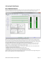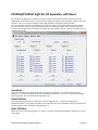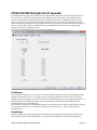
1
USB-to-I2C Software User’s Manual for USB-to-I2C Professional and Elite Hardware Information provided in this document is solely for use with USB-to-I2C Professional and Elite hardware. SB Solutions, Inc. reserves the right to make changes or improvements to this document at any time without notice. We assume no liability whatsoever in the sale or use of this product, including infringement of any patent or copyright. No part of this document may be reproduced or transmitted in any form or by any means, electronic or mechanical, for any purpose, without the express written permission of SB Solutions, Inc. Microsoft and Windows are registered trademarks of Microsoft Corporation. Other brand names are trademarks or registered trademarks of their respective owners. Questions or comments regarding this document should be emailed to [email protected] 2013 SB Solutions, Inc. All rights reserved. USB-to-I2C Elite Software User’s Manual February 2013 Page 2 TABLE OF CONTENTS I²C PROTOCOL .............................................................................................................................................................9 GENERAL CHARACTERISTICS........................................................................................................................................................ 9 BIT TRANSFER ................................................................................................................................................................................ 9 START AND STOP CONDITIONS .................................................................................................................................................. 9 I²C ADDRESS .................................................................................................................................................................................. 9 I²C BUS DOCUMENTATION........................................................................................................................................................... 9 MAIN SCREEN ........................................................................................................................................................... 10 Device Menu .........................................................................................................................................................................10 Message Panel .....................................................................................................................................................................10 Messages: ..............................................................................................................................................................................10 File Menu ...............................................................................................................................................................................11 Save Data ...............................................................................................................................................................................11 Load Data ..............................................................................................................................................................................11 Options Menu ......................................................................................................................................................................11 I²C Frequency Menu Item ..............................................................................................................................................11 Enable 3.3V Output Power ............................................................................................................................................12 Enable 5V Output Power ................................................................................................................................................12 Windows Menu ...................................................................................................................................................................12 Frequency Indicator .........................................................................................................................................................12 MEMORY DEVICES (EEPROM, RAM, FRAM) ................................................................................................... 13 I²C Address ...........................................................................................................................................................................13 Write Page Size Selection ...............................................................................................................................................14 Erase/Write Cycle Time .................................................................................................................................................14 Data Grid ................................................................................................................................................................................14 Byte Address (Subaddress) ...........................................................................................................................................14 Read Byte Button ...............................................................................................................................................................14 Read All Button ...................................................................................................................................................................14 Write Byte Button..............................................................................................................................................................15 Write All Button .................................................................................................................................................................15 Verify Button .......................................................................................................................................................................15 Fill Buffer ...............................................................................................................................................................................15 Checkerboard ......................................................................................................................................................................16 Inverted Checkerboard ...................................................................................................................................................16 Goto Byte... ............................................................................................................................................................................16 Copy Block ............................................................................................................................................................................16 Open and Save Data ..........................................................................................................................................................17 UNIVERSAL INTERFACES...................................................................................................................................... 18 USER DEFINABLE DEVICE...........................................................................................................................................................18 Define New Device ............................................................................................................................................................19 Open Device Definition File ...........................................................................................................................................19 Save ..........................................................................................................................................................................................19 Save As… ................................................................................................................................................................................19 Save Registers in text format ........................................................................................................................................19 Byte Mode .............................................................................................................................................................................19 Print Device Data ...............................................................................................................................................................19 Data Grid ................................................................................................................................................................................19 Edit Menu ..............................................................................................................................................................................19 Edit Current Register .......................................................................................................................................................20 Edit Current Device...........................................................................................................................................................20 Slider Control.......................................................................................................................................................................21 USB-to-I2C Elite Software User’s Manual Page 3 Spin Control..........................................................................................................................................................................21 Bit Control .............................................................................................................................................................................21 EXPERT MODE ..............................................................................................................................................................................22 Open New Page ...................................................................................................................................................................22 Open Data File .....................................................................................................................................................................22 Save Data ...............................................................................................................................................................................22 Close Expert Mode.............................................................................................................................................................22 Add a Row .............................................................................................................................................................................23 Delete a Row ........................................................................................................................................................................23 Clear the current row.......................................................................................................................................................23 Copy the Current Row .....................................................................................................................................................23 Paste Data .............................................................................................................................................................................23 Compress Data ....................................................................................................................................................................23 Send Message ......................................................................................................................................................................24 Send All...................................................................................................................................................................................24 Send Sequence ....................................................................................................................................................................24 Message Editor....................................................................................................................................................................24 Message Number ...............................................................................................................................................................25 Delay after message ..........................................................................................................................................................25 Device Address ...................................................................................................................................................................25 Read/Write Selection.......................................................................................................................................................25 Stop? ........................................................................................................................................................................................25 Message Data .......................................................................................................................................................................25 Notes .......................................................................................................................................................................................25 IO EXPANDERS ......................................................................................................................................................... 26 PCA9500/PCA9501 8-BIT I2C I/O PORT WITH INTERRUPT AND 2K EEPROM ....................................................... 27 Changing I/O Expander Data with Checkboxes ...................................................................................................27 Read I/O Button .................................................................................................................................................................27 Set Data ..................................................................................................................................................................................27 Word Address......................................................................................................................................................................28 Read Byte Button ...............................................................................................................................................................28 Read All Button ...................................................................................................................................................................28 Write Byte Button..............................................................................................................................................................28 Write All Button .................................................................................................................................................................28 PCA9534 EIGHT-BIT LOW POWER I/O PORT WITH INTERRUPT PCA9554(A) EIGHT-BIT I/O PORT WITH INTERRUPT PCA9538 EIGHT-BIT LOW POWER I/O PORT WITH INTERRUPT & RESET .............................................. 29 Automatic Write Enable .................................................................................................................................................29 Checkboxes ...........................................................................................................................................................................29 Edit Boxes .............................................................................................................................................................................30 Read Buttons .......................................................................................................................................................................30 Write Button ........................................................................................................................................................................30 PCA9536 FOUR-BIT IO EXPANDER PCA9537 FOUR-BIT IO EXPANDER WITH INTERRUPT AND RESET ................ 31 Automatic Write Enable .................................................................................................................................................31 Checkboxes ...........................................................................................................................................................................31 Edit Boxes .............................................................................................................................................................................31 PCA9535 SIXTEEN-BIT LOW POWER I/O PORT WITH INTERRUPT PCA9539 SIXTEEN-BIT LOW POWER I/O PORT WITH INTERRUPT & RESET PCA9555 SIXTEEN-BIT I/O PORT WITH INTERRUPT ............................................. 32 Input Registers (subaddress 0x00 and 0x01) .......................................................................................................32 Output Registers (subaddress 0x02 and 0x03) ...................................................................................................32 Polarity Registers (subaddress 0x04 and 0x05) ................................................................................................. 33 Configuration Register (subaddress 0x06 and 0x07) ....................................................................................... 33 Automatic Write Enable .................................................................................................................................................33 Checkboxes ...........................................................................................................................................................................33 Edit Boxes .............................................................................................................................................................................33 Read Buttons .......................................................................................................................................................................33 PCA9556/PCA9557 EIGHT-BIT I/O EXPANDERS WITH RESET ..................................................................................... 34 USB-to-I2C Elite Software User’s Manual Page 4 Auto Write.............................................................................................................................................................................34 Read All Button ...................................................................................................................................................................34 Write All Button .................................................................................................................................................................34 Register 0 (Input Port) ....................................................................................................................................................35 Register 1 (Output port) .................................................................................................................................................35 Register 2 (Polarity) .........................................................................................................................................................35 Register 3 (Configuration) .............................................................................................................................................35 PCA9698 FORTY-BIT I/O EXPANDER ....................................................................................................................................36 Device Configuration ........................................................................................................................................................36 Read All Button ...................................................................................................................................................................36 Write All Button .................................................................................................................................................................36 Bank Registers ....................................................................................................................................................................37 PCF8574/PCF8574A EIGHT-BIT I/O EXPANDER ............................................................................................................38 Checkboxes ...........................................................................................................................................................................38 Read Button..........................................................................................................................................................................38 Read Data ..............................................................................................................................................................................39 Data Byte ...............................................................................................................................................................................39 Write Button ........................................................................................................................................................................39 Automatic Write Enable .................................................................................................................................................39 Auto Read Back ...................................................................................................................................................................39 PCF8575 16-BIT I/O EXPANDER ...........................................................................................................................................40 Read Checkboxes ...............................................................................................................................................................40 Write Checkboxes ..............................................................................................................................................................40 Read Button..........................................................................................................................................................................41 Write Button ........................................................................................................................................................................41 Read Data Boxes .................................................................................................................................................................41 Write Data Boxes ...............................................................................................................................................................41 Auto Write.............................................................................................................................................................................41 LED BLINKERS AND DIMMERS ........................................................................................................................... 42 PCA9530 TWO-BIT I2C LED DIMMER..................................................................................................................................43 Device Address ...................................................................................................................................................................43 Auto Write On/Off Button .............................................................................................................................................43 LED Mode Selector ............................................................................................................................................................43 PWM Period Slidebar .......................................................................................................................................................44 PWM Duty Cycle .................................................................................................................................................................44 Write All Button .................................................................................................................................................................44 Read Input Register ..........................................................................................................................................................44 Read All Button ...................................................................................................................................................................44 PCA9531 EIGHT-BIT I2C LED DIMMER ...............................................................................................................................45 Device Address ...................................................................................................................................................................45 Auto Write On/Off Button .............................................................................................................................................45 LED Mode Selector ............................................................................................................................................................45 PWM Period Slidebar .......................................................................................................................................................45 PWM Duty Cycle .................................................................................................................................................................46 Write All Button .................................................................................................................................................................46 Read Input Register ..........................................................................................................................................................46 Read All Button ...................................................................................................................................................................46 PCA9532 SIXTEEN-BIT I2C LED DIMMER ...........................................................................................................................47 Device Address ...................................................................................................................................................................47 Auto Write On/Off Button .............................................................................................................................................47 LED Mode Selector ............................................................................................................................................................48 PWM Period Slidebar .......................................................................................................................................................48 PWM Duty Cycle .................................................................................................................................................................48 Write All Button .................................................................................................................................................................48 Read Input Register ..........................................................................................................................................................48 Read All Button ...................................................................................................................................................................48 USB-to-I2C Elite Software User’s Manual Page 5 PCA9533 FOUR-BIT I2C LED DIMMER ................................................................................................................................49 Device Address ...................................................................................................................................................................49 Auto Write On/Off Button .............................................................................................................................................49 LED Mode Selector ............................................................................................................................................................50 PWM Period Slidebar .......................................................................................................................................................50 PWM Duty Cycle .................................................................................................................................................................50 Write All Button .................................................................................................................................................................50 Read Input Register ..........................................................................................................................................................50 Read All Button ...................................................................................................................................................................50 PCA9550 TWO-BIT I2C LED BLINKER .................................................................................................................................51 Device Address ...................................................................................................................................................................51 Auto Write On/Off Button .............................................................................................................................................51 LED Mode Selector ............................................................................................................................................................52 PWM Period Slidebar .......................................................................................................................................................52 PWM Duty Cycle .................................................................................................................................................................52 Write All Button .................................................................................................................................................................52 Read Input Register ..........................................................................................................................................................52 Read All Button ...................................................................................................................................................................52 PCA9551 EIGHT-BIT I2C LED BLINKER...............................................................................................................................53 Device Address ...................................................................................................................................................................53 Auto Write On/Off Button .............................................................................................................................................53 LED Mode Selector ............................................................................................................................................................54 PWM Period Slidebar .......................................................................................................................................................54 PWM Duty Cycle .................................................................................................................................................................54 Write All Button .................................................................................................................................................................54 Read Input Register ..........................................................................................................................................................54 Read All Button ...................................................................................................................................................................54 PCA9552 SIXTEEN-BIT I2C LED BLINKER...........................................................................................................................55 Device Address ...................................................................................................................................................................55 Auto Write On/Off Button .............................................................................................................................................55 LED Mode Selector ............................................................................................................................................................55 PWM Period Slidebar .......................................................................................................................................................56 PWM Duty Cycle .................................................................................................................................................................56 Write All Button .................................................................................................................................................................56 Read Input Register ..........................................................................................................................................................56 Read All Button ...................................................................................................................................................................56 PCA9553 FOUR-BIT I2C LED BLINKER ................................................................................................................................57 Device Address ...................................................................................................................................................................57 Auto Write On/Off Button .............................................................................................................................................57 LED Mode Selector ............................................................................................................................................................58 PWM Period Slidebar .......................................................................................................................................................58 PWM Duty Cycle .................................................................................................................................................................58 Write All Button .................................................................................................................................................................58 Read Input Register ..........................................................................................................................................................58 Read All Button ...................................................................................................................................................................58 PCA9633 FOUR-BIT I2C LED DIMMER ................................................................................................................................59 SAA1064 FOUR-DIGIT LED-DRIVER .....................................................................................................................................60 Control Register .................................................................................................................................................................60 Automatic Write .................................................................................................................................................................61 Digits 1, 2, 3, and 4 ............................................................................................................................................................61 Instruction Byte ..................................................................................................................................................................61 Read Address .......................................................................................................................................................................61 Status Register ....................................................................................................................................................................61 Read Status Button............................................................................................................................................................61 Write Button ........................................................................................................................................................................61 MASTER SELECTOR ................................................................................................................................................ 62 USB-to-I2C Elite Software User’s Manual Page 6 PCA9541 2-TO-1 I2C MASTER SELECTOR ...........................................................................................................................62 Register 0: Mask Register ..............................................................................................................................................62 Register 1: Control Register ..........................................................................................................................................62 Register 2: Interrupt Status Register ........................................................................................................................63 Bus control lost interrupt ..............................................................................................................................................63 Recovery/initialization interrupt ...............................................................................................................................63 Downstream interrupt ....................................................................................................................................................63 Functional test interrupt ................................................................................................................................................63 MULTIPLEXER / SWITCHES ................................................................................................................................ 65 PCA9540B/PCA9542A/PCA9544A/PCA9547 ..........................................................................................................66 Control Register .................................................................................................................................................................66 Interrupts ..............................................................................................................................................................................66 Multiplexer Control ..........................................................................................................................................................67 Auto Write.............................................................................................................................................................................67 PCA9543A/PCA9545A/PCA9546A/PCA9548A/PCA9549 ................................................................................. 68 Control Register .................................................................................................................................................................68 Interrupts ..............................................................................................................................................................................68 Channel Selection ..............................................................................................................................................................68 Auto Write.............................................................................................................................................................................69 NON-VOLATILE REGISTERS................................................................................................................................. 70 PCA8550/PCA9559/PCA9560/PCA9561 ...................................................................................................................70 Address Selection ..............................................................................................................................................................70 Data Register .......................................................................................................................................................................70 EEPROM Byte x ...................................................................................................................................................................70 MUX_OUT...............................................................................................................................................................................70 Auto Write.............................................................................................................................................................................71 REAL-TIME CLOCKS................................................................................................................................................ 72 PCF8563 .....................................................................................................................................................................................72 THERMAL MANAGEMENT .................................................................................................................................... 73 LM75A DIGITAL TEMPERATURE SENSOR AND THERMAL WATCHDOG............................................................................... 74 Device Address ...................................................................................................................................................................74 Automatic Write (Checkbox) ........................................................................................................................................74 Write All .................................................................................................................................................................................74 Read All ..................................................................................................................................................................................74 Temperature Register (Temp) ....................................................................................................................................75 Thyst (Hysteresis) Register ..........................................................................................................................................75 TOS (Overtemp shut-down threshold) Register ..................................................................................................75 Configuration Register ....................................................................................................................................................75 Start Read Button ..............................................................................................................................................................75 NE1617(A) TEMPERATURE MONITOR...................................................................................................................................76 Read-Only Registers .........................................................................................................................................................76 Write Only Registers ........................................................................................................................................................76 Auto Write.............................................................................................................................................................................76 SA56004A TEMPERATURE SENSOR .......................................................................................................................................77 SE98 TEMPERATURE SENSOR...................................................................................................................................................78 SLAVE MODE ............................................................................................................................................................. 79 Write to Slave ......................................................................................................................................................................79 Read from Slave ..................................................................................................................................................................80 Enable Slave .........................................................................................................................................................................80 Define Slave Size ................................................................................................................................................................80 Fill Slave Buffer ...................................................................................................................................................................80 Read Slave Buffer ...............................................................................................................................................................80 USB-to-I2C Elite Software User’s Manual Page 7 Idle Slave ...............................................................................................................................................................................80 Resume Slave .......................................................................................................................................................................80 Enable Master......................................................................................................................................................................81 Close ........................................................................................................................................................................................81 TROUBLESHOOTING .............................................................................................................................................. 82 USB-to-I2C Elite Software User’s Manual Page 8 I²C Protocol General Characteristics The I²C protocol allows data to be transferred between devices using two open-drain (or open-collector) bidirectional lines. One line is the serial clock (SCL) and the other is the serial data (SDA). The bus master generates the Start conditions, the clock signals on SCL, as well as the Stop condition. An acknowledge is transmitted on the bus after each byte is sent over the bus. Bit Transfer Data on SDA must be stable while SCL is high. The state of SDA when SCL is high determines the logic level of the transmitted data bit. Start and STOP Conditions Within the procedure of the I²C bus, unique situations arise which are defined as START and STOP conditions. A HIGH to LOW transition on the SDA line while SCL is HIGH is one such unique case. This situation indicates a START condition. A LOW to HIGH transition on the SDA line while SCL is HIGH defines a STOP condition. The master always generates START and STOP conditions. The bus is considered to be busy after the START condition. The bus is considered to be free again a certain time after the STOP condition. I²C Address The first seven bits of an I²C transmission make up the slave address. The eighth bit (or the least significant bit) is the R/W bit that determines the direction of the message. A '0' in the least significant position of the first byte means that the master will WRITE information to the selected slave. A '1' in this position means that the master will READ information from the slave. When an I²C address is sent, each device in a system compares the first seven bits after the START condition with its own address. If they match, the device considers itself addressed by the master as a slave-receiver or slave-transmitter, depending on the R/W bit. When selecting addresses within USB-to-I2C, the software assumes the least significant bit is zero (write). If the I²C message is a write transmission, the least significant bit will be sent as a ‘0’ while if it is a read, the software will append a ‘1’ in the LSB position. I²C Bus Documentation The complete I²C Bus specification can be found at http://www.standardics.nxp.com/literature/i2c/ Main Screen This user manual covers the features of the USB-to-I2C software, for both the USB-to-I2C Professional and Elite hardware. The software for each hardware has similar features, however, the USB-to-I2C software for the Elite and Professional hardware are not compatible, so if you are using both hardware platforms, you will need to install both the Professional and Elite software packages. When the USB-to-I2C program starts, a screen, as shown below, will be displayed on the monitor. Device Menu Options Menu USB Hardware Indicator Message Panel I²C Frequency d Output Power Indicators Device Menu The device menu contains a list of I²C devices supported by the USB-to-I2C software. Selecting the device from this menu may start any of the listed devices. You can have any combination of devices open at one time. Switching between active devices may be accomplished via the Window menu on the main toolbar. Message Panel The main screen has a panel that displays messages from the program. It will indicate if the I²C transmission was successful or if there was a problem encountered. A list of messages is shown below. Messages: Transmission successful - the last I²C transmission was successfully completed. Address not acknowledged - an I²C address was successfully transmitted but no slave device acknowledged the address. A STOP condition is sent after the acknowledge clock pulse if no acknowledge is received. Data not acknowledged - an I²C address was previously acknowledged but one of the following data bytes was not acknowledged. . A STOP condition is sent after the acknowledge clock pulse if no acknowledge is received. Read acknowledged corrupted - the master tried to send a NACK (no acknowledge) for the last read byte in a transmission, but it was corrupted by a low level on SDA by another device on the bus. SDA stuck low - before a START condition is initiated, the software verifies that both the SDA and SCL lines are high. If SDA is stuck low, then an SDA stuck low message will be displayed. SCL stuck low - before a START condition is initiated, the software verifies that both the SDA and SCL lines USB-to-I2C Elite Software User’s Manual Page 10 are high. If SCL is stuck low, then an SCL stuck low message will be displayed. Hardware not detected- is displayed when there is no USB-to-I2C hardware plugged into the PC’s USB port, or if the drivers are not installed correctly.. File Menu Upon starting the USB-to-I2C software, the File menu contains the Exit and Close commands. When a device has been selected from the Device Menu, it is possible that the File Menu will also display device specific commands such as Save As and Load. In User Device mode, previously created device files may be conveniently loaded. Save Data Many devices contain the menu item 'Save Data' under the File menu. The data may be recalled by selecting the Load Data item under the File Menu. Load Data After data has been stored using the 'Save Data' item in the File menu, it can be recalled by selecting the Load Data item. Options Menu The options menu allows you to change the I²C frequency, the 3.3V and 5V power outputs are also controlled from this menu. If you have multiple USB-to-I2C Elite or Professional hardware units connected to your PC, you can select which device you would like to communicate with. I²C Frequency Menu Item The I²C frequency dialog box can be activated by: a. Selecting I²C Frequency in the Options menu b. Double-clicking the frequency indicator on the bottom right corner of the application c. Right-clicking the status bar at the bottom of the application, and then selecting I²C frequency By choosing this menu item, you will activate a dialog box that shows the current I²C frequency. The frequency can be changed by entering a value into the edit box. Pressing the OK button will close the dialog box and will update the I²C frequency panel on the main screen. The SCL High and SCL Low spin controls allow you to fine tune the frequency and also allow you to control the duty cycle of the clock signal. The frequency of the I2C signal can be calculated as: USB-to-I2C Elite Software User’s Manual Page 11 fi2c = 60,000,000 / (SCLHigh + SCLLow). The minimum values for SCLHigh and SCLLow is 12, however, the I2C bus hardware was designed to meet the 400 kHz so operating at higher frequencies cannot be guaranteed since this is dependent upon the user’s application. Enable 3.3V Output Power By selecting the 3.3V Output Power menu item, the USB-to-I2C hardware will supply power to your target system. There is no need to enable this output unless you need to power your target system. When enabled, there will be a checkbox beside the menu item and the status bar at the bottom of the application will have a 3.3V On indicator shown in green. Enable 5V Output Power By selecting the 5V Output Power menu item, the USB-to-I2C hardware will supply power to your target system. There is no need to enable this output unless you need to power your target system. When enabled, there will be a checkbox beside the menu item and the status bar at the bottom of the application will have a 5.0V On indicator shown in green. Windows Menu The Windows Menu contains screen commands such as cascade, tile, arrange all icons, and minimize all. If there are devices active in the program, you will find them listed in this menu. When multiple device types are open, it is easy to move between the device types by clicking on the desired item in this menu. Frequency Indicator The frequency at which the hardware is sending I²C messages over the i2c bus is shown in this box on the main screen. Note that the hardware cannot produce every value you enter so it will set it to the closest available frequency. USB-to-I2C Elite Software User’s Manual Page 12 Memory Devices (EEPROM, RAM, FRAM) Upon starting any memory type device, you will see a screen similar to the one shown below. Note that RAM/FRAM will be similar to EEPROM but it will not have a Page Size or Write Time. I²C Address A drop-down menu is provided which allows the user to select a valid address for the selected device type. USB-to-I2C Elite Software User’s Manual Page 13 Write Page Size Selection The Page Write Size defines the number of bytes that may be written in a single erase/write programming cycle. Smaller devices generally use an 8 or 16-byte pages while larger devices use up to 128 bytes per page. Check the device datasheet to find the appropriate page write size for the device you are programming. If you do not know the page size, use a small page size such as 8 bytes. A smaller page size will require a longer total programming time for a device. Erase/Write Cycle Time Programming software must allow a certain period of time to elapse after writing a block of data to an EEPROM. This time is device dependent but is normally between 5ms and 40ms. A STOP condition must be performed before the erase/write cycle commences. Most EEPROMs will not respond to their address until the erase/write cycle has been completed. Data Grid The data grid consists of rows and columns. Each cell within the grid contains a two digit hexadecimal number. Each cell corresponds to a physical byte location within the memory device. For example, in the diagram below, cell 0x21 is highlighted (row 2, column 1). This translates to address 33 (decimal) in the device. The program calculates the physical address for you and displays it at the left side of the screen in the box labeled ‘Word Address’ or ‘Subaddress’. Byte Address (Subaddress) The byte address (sometimes called subaddress or word address) is a pointer to a register or memory location within the I²C device. To access this location, the software will send out the device I²C address, followed by this byte address, followed by the read or write data. The program displays the byte address of the active cell of the memory grid in both hexadecimal and decimal notation. Read Byte Button Pressing the 'Read Byte' button initiates a read from the I²C device. The program begins the transmission by writing the device address, followed by the current byte address. A Repeated Start is then generated, followed by the device’s read address, and finally a read of a single data byte. The result of each byte read is immediately entered in the appropriate cell in the grid. Alternatively, you may press the <Alt> and <b> keys simultaneously to achieve the same results. Read All Button Pressing the 'Read All' button initiates a read from the I²C device. The program begins the transmission by writing the device address, then the byte address 0x00. A Repeated Start is then generated, followed by sequential reads of the entire device. In addition to pressing the USB-to-I2C Elite Software User’s Manual Page 14 'Read All' button, you may press the <Alt> and <r> keys simultaneously to achieve the same results. Write Byte Button Pressing the 'Write Byte' button initiates a Write to the I²C device. The program begins the transmission by writing the slave address and then the word address of the currently active cell in the grid. The selected data byte is then sent. In addition to pressing the 'Write Byte' button, you may press the <Alt> and <y> keys simultaneously and achieves the same results. Write All Button Pressing the 'Write All' button initiates a Write to the I²C device. The program begins the transmission by writing the byte address 0x00 to the device and sequentially writes the entire device. For a RAM type device, the data is sent in one long message. In the case of an EEPROM, the software will send one page of data (usually 8 bytes but check the datasheet for the particular device you are addressing) followed by a STOP condition. Following the STOP condition, the program waits a length of time, determined by the Erase/Write cycle time of the device (again check the datasheet for the device you are programming), before writing another page to the device. In addition to pressing the 'Write All' button, you may press the <Alt> and <w> keys simultaneously to achieve the same results. After completion of the write cycle, the USB-to-I2C software will read the entire device to verify that the contents of the device match the data that was sent. An error message will be displayed if the data read from the device does not match the data in the on-screen buffer. Verify Button Pressing the ‘Verify’ button initiates a read of the entire EEPROM. After reading the contents of the EEPROM, USB-to-I2C will compare the contents with the values in the grid. An error will be flagged if the contents of the EEPROM do not match the contents of the USB-to-I2C on-screen grid. Fill Buffer The grid will be filled with the two digit hexadecimal number found in the ‘Fill with’ edit box when the Fill Buffer button is pressed. The fill can be constrained to the addresses found in the ‘Fill from’ to the ‘Fill to’ edit boxes. No information will be sent over the I²C bus. USB-to-I2C Elite Software User’s Manual Page 15 Checkerboard The grid will be filled an alternating ‘1’ and ‘0’ pattern when this is chosen from the Fill with Checkerboard selection is made on the Edit menu. Inverted Checkerboard The grid will be filled an alternating ‘0’ and ‘1’ pattern when this is chosen from the Fill with Inverted Checkerboard selection is made on the Edit menu. Go To Byte... When the Go To Byte menu selection is made from the Edit menu, a dialog box is displayed where a hex or decimal address may be entered. When the OK button is pressed the grid location with the desired address is shown. This is useful when you don’t want to scroll through to find a specific data location. Copy Block It is possible to copy a block of data from one on-screen buffer area to another using the Copy Block function. Simply define the data to be copied using the ‘Copy From’ edit boxes and then enter the address where the data is to be copied to. The ending address is calculated automatically by the software and is not editable by the user. Pressing the Copy Block button starts the copying process. USB-to-I2C Elite Software User’s Manual Page 16 Open and Save Data Data can be saved for later use in one of four formats: mem: this format places the raw data in a file (similar to a bin file) but also saves the device configuration (device size, address, page size, and write time). hex: standard Intel hex file format bin: binary file. csv: comma separated variables USB-to-I2C Elite Software User’s Manual Page 17 Universal Interfaces User Definable Device The User Definable Device allows you to define your own I²C device and then enables the user to change the values of the individual cells within the grid using various controls such as sliders and spin controls. When the User Definable Device is first opened, a 256 byte device grid is shown on the screen but does not have any names associated with the data, and all the data bytes are set to 0xFF. A previously defined device may be loaded by selecting it from the Most Recently Used files at the bottom of the File menu. If devices have not yet been defined, there will be no devices shown below the File/Exit menu item. To begin the definition process, you may right click with your mouse on any data cell in the grid or select 'Current Device' or 'Current Cell' from the Edit menu. The Reset item in the Edit menu will clear all the register names to 'Undefined Register' and set the data values to 0xFF. Clicking on the desired cell and doing one of the following can change the data value of the individual cells: 1. Typing in a two digit hexadecimal number. 2. Assigning a slider to the active cell by pressing the Slider button. 3. Assigning a spin control to the active cell by pressing the Spinner button. 4. Assigning a Bit-wise control to the active cell by pressing the Bit-wise button. Items 2, 3, and 4 can also be achieved by positioning the cursor over the desired cell and right clicking on the grid to select the appropriate control from the pop-up menu. USB-to-I2C Elite Software User’s Manual Page 18 Define New Device This is similar to the Edit Current Device (explained below). This menu selection allows the user to start a new device from scratch. All register names are undefined and all default values are 0xFF. Open Device Definition File A previously saved device definition file (.def) can be recalled by selecting this menu item. The device definition file contains the Device Name, Device Address, Register Names, and Register Values. Save Device definition files can be saved to disk by selecting the Save menu item. Save As… Use the Save As dialog box to change the definition file name or to save the definition file in a new location. If the file name already exists, USB-to-I2C asks if you want to replace the existing file. Save Registers in text format The device definition files are not in a format that can easily be used by the user, therefore, USB-to-I2C allows you to save the information in a text format (extension .txt). Users can then open and edit this file with any word processor such as Notepad or WordPad. The text files are for the user’s information only and cannot be read by USB-to-I2C. Byte Mode When the Write All and Read All buttons are pressed, the software assumes that the subaddress is autoincremented after each data byte is written or read. For example, if you have a four byte device, the writing sequence would be Start-Address-Subaddress0-data0-data1-data2-data3-Stop. Many devices do not autoincrement the subaddress between data bytes and require that only one data byte is sent for each transmission. In these situations, click on the Byte Mode check box. The writing sequence would be StartAddress-Subaddress0-data0-Stop. The sequence would be repeated for each data byte. Print Device Data A print out of the register definitions can be obtained by selecting this option from the File menu. Data Grid The grid consists of rows and columns. Each cell within the grid contains a two digit hexadecimal number. Each cell corresponds to a physical byte location within the I²C device. For example, in the diagram shown above, cell 0x07 is highlighted (row 0, column 7). This translates to address 7 (decimal) in the device (assuming the first byte is address 0x00). The data may be changed by entering hexadecimal numbers from your keyboard. Non-valid keys will be ignored. In order to edit the entire grid, including the name and default values of the registers, you may right click on the grid or select the appropriate item from the Edit menu. The individual cells within the grid will be blue if the cell's subaddress is greater than the maximum number of registers defined for the active device. The number of device registers may be changed at any time in the ‘Edit Current Device’ screen. Edit Menu The Edit menu is available only when the User Definable Device screen is active. The user can select from one of the three menu items: 1. Current Device - brings up a screen showing the all the register data for the active device. 2. Current register - allows registers to be changed one at a time. 3. Reset grid - all register data will be set to 0xFF and the register descriptions will be 'Undefined Register' USB-to-I2C Elite Software User’s Manual Page 19 Edit Current Register If you want to adjust one register in the grid, use the 'Edit Current Register' screen. This screen can be started by right clicking on the User Definable Device grid or by selecting Current Register from the Edit menu. The name of the register and the initial value displayed, when the definition file is first opened, can be changed here. Note that the register name changes are not saved until the ‘Save’ or ‘Save As.. .’ item (under the File menu) is selected. Edit Current Device Editing the current device may be accomplished by clicking on 'Edit Current Device' from the Edit menu, or by right clicking on the grid within the User Definable Device mode of USB-to-I2C. The screen, shown above will be displayed when either method is invoked. Device Name: the name entered in this box will be shown in the title bar of USB-to-I2C when the definition file is opened. Device Address: is the device I²C address that will be displayed in the Address box when the definition file is opened. Note that only even addresses are valid here. USB-to-I2C will append the appropriate R/W bit at the end of the address depending upon the operation to be performed (the last bit will be a '1' if it is a read operation and a '0' if it is a write). Number of Registers: Enter the number of registers the device contains. The size of the data entry grid will be modified to accommodate the number of registers. Fill: This box should be modified only if you want to initialize all the registers to one particular value. OK button: the data entered by the user in the 'Edit Current Device' screen will be transferred to the User Definable Device screen. Cancel button: the editing session will be closed and no changes to the User Definable Device screen will occur. Note that any changes are not saved until the ‘Save’ or ‘Save As…’ menu item is selected. USB-to-I2C Elite Software User’s Manual Page 20 Slider Control The Slider Control is activated when the user presses the Slider button on the User Defined Device screen or by right clicking the grid and then selecting 'Change Active Register with Slider Control' from the pop-up menu. The subaddress of the active cell in the grid will be assigned to the Slider. The subaddress is shown in the upper left corner. Moving the slider bar up and down will cause the value of that cell to be changed. If Auto Write On is checked, then the contents of the cell will be transmitted to the device subaddress when it is changed. If an error is encountered while transmitting using Auto Write, USB-to-I2C will turn off Auto Write and it will be up to the user to fix the error condition and re-enable Auto Write. It should be noted that the Slider Control always stays on top of all other devices within USB-to-I2C. Spin Control The Spin Control is activated when the user presses the Spinner button on the User Defined Device screen or by right clicking the grid and then selecting 'Increment/Decrement Current Register with a Spin Control' from the pop-up menu. The subaddress of the active cell in the grid will be assigned to the Spin Control. The subaddress is shown in the upper left corner. Clicking on the spin control's up or down arrow will cause the value of that cell to be incremented or decremented. If Auto Write On is checked, then the contents of the cell will be transmitted to the device subaddress when it is changed. . If an error is encountered while transmitting using Auto Write, USB-to-I2C will turn off Auto Write and it will be up to the user to fix the error condition and re-enable Auto Write. It should be noted that the Spin Control always stays on top of all other devices within USB-to-I2C. Bit Control The Bit Control is activated when the user presses the Bit Control button on the User Defined Device screen or by right clicking the grid and then selecting 'Use Bit Control to Change Active Register' from the pop-up menu. The subaddress of the active register in the grid will be assigned to the Bit Control. The subaddress is shown in the upper left corner. Clicking on any of the eight edit boxes will cause the value of that bit to be inverted. If Auto Write On is checked, then the contents of the cell will be transmitted to the device subaddress when it is changed. It should be noted that the Bit Control always stays on top of all other devices within USB-to-I2C. USB-to-I2C Elite Software User’s Manual Page 21 Expert Mode The figure below shows the Expert Mode screen. Open New Page Pressing this button opens a new blank page. There will be 8 empty rows (messages). Selecting ‘New’ from the ‘File’ menu while the Expert Mode is active will perform the same function. Open Data File A previously saved data file can be recalled by pressing the Open Data File button or by selecting Open from the File menu while the Expert Mode is active. A dialog box will be displayed allowing the user to navigate to the appropriate directory. Save Data The current data will be saved when this button is pressed. The user specifies the name and location of the file in a dialog box that is displayed after the button is pressed. A dialog box will be displayed which allows the user to navigate to the appropriate directory. The user can also perform the same function by selecting Save from the File menu while the Expert Mode screen is active. Close Expert Mode The Expert Mode screen is closed but USB-to-I2C will not be terminated. USB-to-I2C Elite Software User’s Manual Page 22 Add a Row Inserts a new (blank) row after the active row. You can also use the Ctrl+Insert keyboard shortcut to insert a new row. The total number of rows is limited to 64. Delete a Row Deletes the Active Row (active message). You can also use the Ctrl+Del keyboard shortcut to delete the current row. Clear the current row The current row (message) will be cleared. The row will not be deleted but will appear blank. You can also use the Shift+Del keyboard shortcut to clear the current row. Copy the Current Row The current row (message) will be copied. Use the Paste command to paste it to a different row. You can also use the Ctrl+C keyboard shortcut to copy the current row. Paste Data Previously copied data will be pasted into the current row (message). You can also use the Ctrl+V keyboard shortcut to paste the clipboard into the current row. Compress Data All blank rows will be eliminated from the display. Here is an example of a display before compress: USB-to-I2C Elite Software User’s Manual Page 23 And here is the same screen after the compress: It is not required to perform a compress but it does speed up the message transfer process since the application does not need to evaluate blank rows to see if there is data to be sent. Send Message The current message will be sent when this button is pressed. The current message number is shown below the Send Message button. To change the active message to be sent, single-click on the row of the data to be sent. Send All All the valid messages on the screen will be sent in order of the row number. The action will be performed one time. A message is valid if there is a minimum of an address within the message. Since the program tests for a valid message on each line within the message grid before sending the message, it is recommended (not required) to compress the data (see Compress Data above) to speed up the transfer. Send Sequence A sequence of messages will be sent when the Send Sequence button is pressed. The sequence editor is invoked by double-clicking on the sequence display. The sequence length can be up to 64 messages in length. The sequencer is limited to using messages 1 through 64. The Sequence Editor is shown below. Message Editor The i2c message cannot be edited directly in the Expert mode screen. Instead, an Expert Mode Editor is brought up either by double-clicking on a message or when the user attempts to type directly into one of the rows (messages) in the Expert Mode screen. USB-to-I2C Elite Software User’s Manual Page 24 Message Number The message being edited is shown at the top of the message editor screen. Delay after message A delay, measured in milliseconds, can be inserted after a message. Device Address The I2C slave address is entered in the address box in hexadecimal notation. The least significant bit of the address is not important (can be a ‘1’ or ‘0’) since the Expert Mode will ensure that this is appropriate for the read/write transaction when the message is actually transmitted. Read/Write Selection The user can select a Read or Write transaction from the drop-down selection box. If a Read is chosen, then the ‘Number of Bytes to Read’ box will be shown and the data entry area will be hidden. If a Write is chosen, the ‘Number of Bytes to Read’ will be hidden and the data entry area will be shown. Stop? Sending a Stop condition after a message is optional. Normally, it is advisable to send the Stop condition. If a Stop condition is not sent, the clock line will be held low until the next message is sent. If a Stop is not sent, the next message will begin with a Restart condition rather than a Start condition. Message Data The Message Data area contains the location where the user can enter up to 128 data bytes in hexadecimal format. Blank data bytes will be ignored. Notes The information in the Notes section is optional, and is not used by the USB-to-I2C software. USB-to-I2C Elite Software User’s Manual Page 25 IO Expanders The USB-to-I2C supports at least 32 IO Expanders. USB-to-I2C Elite Software User’s Manual Page 26 PCA9500/9501 8-bit I/O port with interrupt and 2k EEPROM The PCA9500 and PCA9501 are 8-bit I/O expanders with an on-board 2-kbit EEPROM. The eight quasi bidirectional data pins can be independently used as inputs or outputs to monitor board level status or activate indicator devices such as LEDs. The data for each Input or Output is kept in the corresponding Input or Output register. The system master can read all registers. Changing I/O Expander Data with Checkboxes The ports, labeled P7 – P0 can be set high or low by clicking on them with a mouse. A high logic level is indicated with a light green color while a low logic level is shown as a dark green color. If a port state is changed, the data byte box in the write area will be updated to reflect the changes. The new data can be sent to the PCA950x by pressing the Write Button. If the Auto Write On is enabled (light green), any change in the state of the Write checkboxes or Write Data Byte will immediately be sent to the PCA950x. Read I/O Button Upon pressing the Read Button, the program will update the hexadecimal data shown beside the Write I/O button as well as show the state of the individual I/Os. The I/O port is low if the port is shown in dark green and is high if it is light green. Set Data All the cells of the memory grid will be filled with the two digit hexadecimal number found in the Preset edit USB-to-I2C Elite Software User’s Manual Page 27 box when the Set Data button is pressed. No information will be sent over the I²C bus. Word Address The Word Address (also called subaddress) is a pointer to a register or memory location within the I²C device. To access this location, the software will send out the device I²C address, followed by this subaddress, followed by the read or write data. The program displays the subaddress of the active cell of the memory grid in both hexadecimal and decimal notation. Read Byte Button Pressing the 'Read Byte' button initiates a read from the I²C device. The program begins the transmission by writing the word address, found in the Word Address or Subaddress box, to the device. The word address of the currently selected cell is shown in the Word Address box on the screen. A Repeated Start is then generated, followed by a read of the single byte. The result of each byte read is immediately entered in the appropriate cell in the grid. In addition to pressing the 'Read Byte' button, you may press the <Alt> and <b> keys simultaneously to achieve the same results. Read All Button Pressing the 'Read All' button initiates a read from the I²C device. The program begins the transmission by writing the word address 0 to the device. A Repeated Start is then generated, followed by sequential reads of the entire device. In addition to pressing the 'Read All' button, you may press the <Alt> and <r> keys simultaneously to achieve the same results. Write Byte Button Pressing the 'Write Byte' button initiates a Write to the I²C device. The program begins the transmission by writing the slave address and then the word address of the currently active cell in the grid. The selected data byte is then sent. In addition to pressing the 'Write Byte' button, you may press the <Alt> and <y> keys simultaneously and achieves the same results. Write All Button Pressing the 'Write All' button initiates a Write to the I²C device. The program begins the transmission by writing the word address 0 to the device and sequentially writes the entire device. The software will send one page of data (4 bytes) followed by a STOP condition. An erase/write cycle is performed before writing another page to the device. In addition to pressing the 'Write All' button, you may press the <Alt> and <w> keys simultaneously to achieve the same results. After the completion of the write cycle, USB-to-I2C will read the entire device to verify that the contents of the device match the data that was sent. An error message will be displayed if the data is not verified. USB-to-I2C Elite Software User’s Manual Page 28 PCA9534 Eight-Bit Low Power I/O Port with Interrupt PCA9554(A) Eight-Bit I/O Port with Interrupt PCA9538 Eight-Bit Low Power I/O Port with Interrupt & Reset The PCA9534, PCA9554(A), and PCA9538 are 16-pin CMOS devices that provide 8 bits of General Purpose parallel Input/Output (GPIO) expansion for I2C/SMBus applications The PCA9554 and PCA9554A are similar devices but respond to different i2c addresses. The PCA9534 differs from the PCA9554(A) in that it does not have pull-up resistors on the outputs. The PCA9538 includes a reset input. The four devices have four internal registers. All four registers can be read by the bus master while the Input register can only be read. Automatic Write Enable When Auto Write is enabled (light green), any changes made to Registers 1, 2, or 3 checkboxes will cause the program to write the new data to the device. The display will read 'Auto Write Off' in when it is disabled and 'Auto Write On' in when enabled. Checkboxes The checkboxes indicate the logic level of the various bits in the registers. A checked box is equivalent to logic ‘1’ while an unchecked box is equivalent to logic ‘0’. The logic level can be changed by single clicking on the checkbox. If Auto Write is enabled (checked), USB-to-I2C will write the new value to the device shown in the Address box. The checkboxes will also be updated when a new value is read by USB-to-I2C, or when the value in the edit boxes is changed. USB-to-I2C Elite Software User’s Manual Page 29 Edit Boxes The edit boxes show the current hexadecimal value for each of the 4 registers. Register 0 is a Read-Only register so the user cannot change this value. If the hexadecimal value is changed by the user, it will be transmitted by USB-to-I2C if the Auto Write is enabled (checked). The checkboxes will also be updated to reflect any changes to the values of the Edit Box. Read Buttons After pressing one of the Read Buttons, USB-to-I2C will read the appropriate register and place the hexadecimal value in the edit box. The checkboxes are updated to reflect the individual bit logic levels. Pressing the Read All button reads all four registers. Because the PCA9554(A), PCA9534, and PCA9538 do not automatically increment the register address between operations, only one register may be read in each transaction. Therefore, after Register 0 has been read, USB-to-I2C will begin a new transaction for each of the other registers. This will continue until all four registers have been read. Write Button Upon pressing one of the Write Buttons, USB-to-I2C will write to the appropriate register. Pressing the Write All button writes to Registers 1, 2, and 3. Since there is no automatic increment of the register subaddress between writes, only one register may be written for each Start condition. Therefore, after Register 1 has been written by USB-to-I2C, a new transaction will be sent out so that Register 2 can be written, followed by Register 3. USB-to-I2C Elite Software User’s Manual Page 30 PCA9536 Four-Bit IO Expander PCA9537 Four-Bit IO Expander with Interrupt and Reset The PCA9536 is an 8-pin and the PCA9537 is a 10-pin CMOS device that provide 4 bits of general purpose parallel Input/Output (GPIO) expansion for I2C and SMBus applications The PCA9536 and PCA95537 are similar devices; however, the PCA9537 adds an interrupt output and a reset input. The PCA9536 and PCA9537 have four registers. All four registers can be read by the bus master while the Input register can only be read. Automatic Write Enable When Auto Write is enabled (checked), any changes made to Registers 1, 2, or 3 checkboxes will cause the program to write the new data to the device. Checkboxes The checkboxes indicate the logic level of the various bits in the registers. A checked box is equivalent to logic ‘1’ while an unchecked box is equivalent to logic ‘0’. The logic level can be changed by single clicking on the checkbox. If Auto Write is enabled (checked), the new value will immediately be written to the device shown in the Address box. The checkboxes will also be updated when a new value is read by USB-to-I2C, or when the value in the edit boxes is changed. Edit Boxes The edit boxes show the current hexadecimal value for each of the 4 registers. Register 0 is a Read-Only register so the user cannot change this value. If the hexadecimal value is changed by the user, it will be transmitted by USB-to-I2C if the Auto Write is enabled (checked). The checkboxes will also be updated to reflect any changes to the values of the Edit Box. USB-to-I2C Elite Software User’s Manual Page 31 PCA9535 Sixteen-Bit Low Power I/O Port with Interrupt PCA9539 Sixteen-Bit Low Power I/O Port with Interrupt & Reset PCA9555 Sixteen-Bit I/O Port with Interrupt The PCA9555, PCA9535, and PCA9539 are 24-pin CMOS device that provide 16 bits of General Purpose parallel Input/Output (GPIO) expansion for I2C/SMBus applications and were developed to enhance the NXP family of I2C I/O expanders. The improvements include higher drive capability, 5V I/O tolerance, lower supply current, individual I/O configuration, and smaller packaging. I/O expanders provide a simple solution when additional I/O is needed for ACPI power switches, sensors, pushbuttons, LEDs, fans, etc. These devices consist of pairs of 8-bit registers: Configuration (Input or Output); Input, Output and Polarity inversion (Active high or Active low operation) registers. The system master can enable the I/Os as either inputs or outputs by writing to the I/O configuration bits. The data for each Input or Output is kept in the corresponding Input or Output register. The polarity of the read register can be inverted with the Polarity Inversion Register. All registers can be read by the system master. Input Registers (subaddress 0x00 and 0x01) These registers are read-only. They reflect the incoming logic levels of the pins, regardless of whether the pin is defined as an input or an output by the Configuration Registers. Writes to this register have no effect. Output Registers (subaddress 0x02 and 0x03) These registers reflect the outgoing logic levels of the pins defined as outputs by the Configuration Registers. Bit values in this register have no effect on pins defined as inputs. Reads from this register return the value that is in the flip-flop controlling the output selection, NOT the actual pin value. USB-to-I2C Elite Software User’s Manual Page 32 Polarity Registers (subaddress 0x04 and 0x05) These registers allow the user to invert the polarity of the Input Port Register data. If a bit in this register is set (written with ‘1’), the corresponding Input Port data is inverted. If a bit in this register is cleared (written with a ‘0’), the Input Port data polarity is retained. Configuration Register (subaddress 0x06 and 0x07) The Configuration Registers define the directions of the I/O pins. If a bit in these register is set, the corresponding port pin is enabled as an input with high impedance output driver. If a bit in these registers is cleared, the corresponding port pin is enabled as an output. At reset, the I/Os are configured as inputs with a weak pull-up to VDD. Automatic Write Enable When Auto Write On is enabled (green), any changes made to Registers 1 through 7 checkboxes will cause the program to write the new data to the PCA9555. The display will read 'Auto Write Off' when it is disabled and 'Auto Write On' when enabled. Checkboxes The checkboxes indicate the logic level of the various bits in the registers. A checked box is equivalent to logic ‘1’ while an unchecked box is equivalent to logic ‘0’. The logic level can be changed by single clicking on the checkbox. If Auto Write is enabled (green LED), USB-to-I2C will write the new value to the PCA9555 immediately after a change is made. Edit Boxes The edit boxes show the current hexadecimal value for each of the 4 registers. Register 0 is a Read-Only register so the user cannot change this value. If the hexadecimal value is changed by the user, it will be transmitted by USB-to-I2C if the Auto Write is on (checked). The checkboxes will also be updated to reflect the new value of the Edit Box. Read Buttons Upon pressing one of the Read Buttons, USB-to-I2C will read the appropriate register and place the hexadecimal value in the edit box. The checkboxes are updated to reflect the individual bit logic levels. USB-to-I2C Elite Software User’s Manual Page 33 PCA9556/PCA9557 Eight-bit I/O Expanders with Reset The PCA9556 and PCA9557 are CMOS circuit that provides parallel input/output expansion for I2C and SMBus applications. These devices consist of an 8-bit input port register, 8-bit output port register, and an I2C interface. It has low current consumption and a high impedance open drain output pin, I/O0. The system master can reset the PCA9556 in the event of a timeout by asserting a LOW on the reset input. The system master can also invert the PCA9556/PCA9557 inputs by writing to their active HIGH polarity inversion bits. Finally, the system master can enable the I/Os as either inputs or outputs by writing to the I/O configuration register. Auto Write When the Auto Write On is enabled (green), any changes made by the user to the PCA9556/PCA9557 Registers 1, 2, and 3 will immediately be sent to the PCA9556/PCA9557. If an error is encountered during this transmission, Auto Write Off will be displayed (red). Read All Button Each time the Read All button is pressed, the contents of Registers 0, 1, 2, and 3 are read from the PCA9556/PCA9557. The register data will be reflected in the state of the checkboxes, with an unchecked box indicating logic '0' and a checked box indicating logic '1'. Write All Button When this button is pressed, Registers 1, 2, and 3 are written to the PCA9556/PCA9557. Register 0 is a readonly register. USB-to-I2C Elite Software User’s Manual Page 34 Register 0 (Input Port) This register is an input-only port. It reflects the incoming logic levels of the pins, regardless of whether the pin is defined as an input or an output by register 3. Writes to this register have no effect. Logic '0' is shown as an unchecked checkbox while logic '1' is shown as a checked box. Register 1 (Output port) This register is an output-only port. It reflects the outgoing logic levels of the pins defined as outputs by register 3. Bit values in this register have no effect on pins defined as inputs. In turn, reads from this register reflect the value that is in the flip-flop controlling the output selection, NOT the actual pin value. Register 2 (Polarity) This register enables polarity inversion of pins defined as inputs by register 3. If a bit in this register is set (written with ‘1’), the corresponding port pin’s polarity is inverted. If a bit in this register is cleared (written with a ‘0’), the corresponding port pin’s original polarity is retained. Register 3 (Configuration) This register is an input-only port. It reflects the incoming logic levels of the pins, regardless of whether the pin is defined as an input or an output by register 3. Writes to this register have no effect. This register configures the directions of the I/O pins. If a bit in this register is set (written with ‘1’), the corresponding port pin is enabled as an input with high impedance output driver. If a bit in this register is cleared (written with ‘0’), the corresponding port pin is enabled as an output. USB-to-I2C Elite Software User’s Manual Page 35 PCA9698 Forty-bit I/O Expander The PCA9698 provides 40-bit parallel input/output (I/O) port expansion for I2C-bus applications organized in five banks of eight I/Os. At 5 V supply voltage, the outputs are capable of sourcing 10 mA and sinking 25 mA with a total package load of 1 A to allow direct driving of 40 LEDs. Any of the 40 I/O ports can be configured as an input or output. The device is fully configurable: output ports can be programmed to be totem-pole or open-drain and logic states can change at either the Acknowledge (bank change) or the Stop Command (global change), each input port can be masked to prevent it from generating interrupts when its state changes, I/O data logic state can be inverted when read by the system master. An open-drain interrupt output pin (INT) allows monitoring of the input pins and is asserted each time a change occurs in one or several input ports (unless masked). The Output Enable pin (OE) 3-states any I/O selected as output and can be used as an input signal to blink or dim LEDs (PWM with frequency > 80 Hz and change duty cycle). Due to the number of registers in the PCA9698, the application interface is split into multiple pages. Device Configuration The first page of controls includes the OUTCONF, ALLBNK, and MODE registers. Read All Button The Read All button will read all the registers in the PCA9698, not only the registers shown on the active page. Write All Button The Write All button will write all the registers in the PCA9698, not only the registers shown on the active page. USB-to-I2C Elite Software User’s Manual Page 36 Bank Registers Each eight bit IO within the PCA9698 has a separate page with the five registers used to control it. USB-to-I2C Elite Software User’s Manual Page 37 PCF8574/PCF8574A Eight-bit I/O Expander The PCF8574 provides general-purpose remote I/O expansion for most microcontroller families via the I²C bus. The device consists of an 8-bit quasi bi-directional port and an I²C interface. The PCF8574 has low current consumption and includes latched outputs with high current drive capability for directly driving LEDs. It also possesses an open-drain interrupt output that can be connected to the interrupt logic of the microcontroller. By sending an interrupt signal on this line, the remote I/O can inform the microcontroller if there is incoming data on its ports without having to communicate via the I²C bus. This means that the PCF8574 can remain a simple slave device. The PCF8574 and PCF8574A differ only in their slave addresses. Checkboxes The checkboxes, labeled P0 - P7, in the write areas of the PCF8574(A) screen can be checked/unchecked by clicking on them with a mouse. If a checkbox state is changed, the data byte box in the write area will be updated to reflect the changes. The new data can be sent to the PCF8574(A) by pressing the Write Button. If the Auto Write On is checked, any change in the state of the Write checkboxes or Write Data Byte will immediately be sent to the PCF8574(A). The checkboxes found in the Read PCF8574(A) panels are read only and can only be changed by the software by clicking the Read buttons. If a checkbox is checked, this indicates logic '1', while an unchecked box indicates logic '0'. Read Button Upon pressing the Read Button, the program will update the hexadecimal data shown beside the button as well as show the state of the individual I/Os. The I/O is low if the checkbox is unchecked and high if it is USB-to-I2C Elite Software User’s Manual Page 38 checked. Read Data The Read boxes on the PCF8574(A) screens are read-only. The user cannot change the contents of any edit boxes or checkboxes in this area. The information is updated only by pressing the Read Button. Data read from the PCF8574(A) will be shown in the box beside the Read Button. The checkboxes are then changed to show the value of each individual I/O of the device. If the checkbox is checked, then the I/O pin is high while an unchecked box means that the I/O pin is low. It is important to remember that before any I/Os in the PCF8574(A) can be used as inputs, they must be set high first. The program does not do this for you. Data Byte Any two digit hexadecimal number may be entered in this data box. When it is changed, the checkboxes labeled P0 - P7 will also change showing the current value of the data which will be written to the PCF8574(A). Write Button Pressing the Write Button will send an I²C message to the PCF8574(A) consisting of: a Start condition, the I²C address, the data byte, followed by the Stop condition. Note that if Automatic Write Enable is checked, any changes to the data box will be sent any time a change is made. Automatic Write Enable When Auto Write On is enabled (light green), any changes made to the P0-P7 checkboxes will cause the program to write the new data to the PCF8574(A). The display will read 'Auto Write Off' when it is disabled and 'Auto Write On' when enabled. Auto Read Back When this function is enabled (light green), the software will immediately read the PCF8574 after it has performed a write. The result of the read will be displayed in the Read groupbox. USB-to-I2C Elite Software User’s Manual Page 39 PCF8575 16-bit I/O Expander The PCF8575 is a CMOS circuit which provides general purpose remote I/O expansion for most microcontroller families via the two-line bi-directional bus (I²C-bus). The device consists of a 16-bit quasi bi-directional port and an I²C-bus interface. The PCF8575 has a low current consumption and includes latched outputs with high current drive capability for directly driving LEDs. It also possesses an interrupt line (INT) which can be connected to the interrupt logic of a microcontroller. By sending an interrupt signal on this line, the remote I/O can inform the microcontroller if there is incoming data on its ports without having to communicate via the I²C bus. This means that the PCF8575 is an I²C-bus slave transmitter/receiver. Every data transmission from the PCF8575 must consist of an even number of bytes; the first byte will be referred to as P07 to P00 and the second byte as P17 to P10. The third will be referred to as P07 to P00 and so on. Read Checkboxes There are sixteen checkboxes in the Read box. The contents of the PCF8575 are read by pressing the Read button. A checked item indicates logic '1' while an unchecked item means logic '0'. The user cannot change the checkboxes since these are read-only. Write Checkboxes Clicking on the checkboxes will invert the current state of the bit. Logic '0' is shown as an unchecked box while logic '1' is shown as a checked box. If Auto Write is on, then any changes made to these checkboxes will immediately be sent to the PCF8575. USB-to-I2C Elite Software User’s Manual Page 40 Read Button When this button is pressed, the two eight bit registers are read via the I²C bus. Data from Port 0 is read first, followed by Port 1. The data bytes are displayed in the area beside the Read button and the checkboxes are updated. Write Button When the Write button is pressed, the contents of the High and Low data boxes are sent to the PCF8575 via the I²C bus. Read Data Boxes These two boxes show the port state of the PCF8575 in hexadecimal format. These boxes cannot be directly modified by the user but must be changed by pressing the read button. Write Data Boxes The user can change the contents of the register by entering a two digit hexadecimal number into the upper and/or lower edit boxes. If the Auto Write is enabled, both data registers are sent, even if only one is changed. Auto Write When the Auto Write is enabled, any changes made by the user to the PCF8575 checkboxes on the screen will immediately be sent to the PCF8575 via the I²C bus. USB-to-I2C Elite Software User’s Manual Page 41 LED Blinkers and Dimmers The USB-to-I2C software supports 18 common LED blinkers and dimmers. USB-to-I2C Elite Software User’s Manual Page 42 PCA9530 Two-bit I2C LED Dimmer The PCA9530 LED Blinker blinks LEDs in I2C applications where it is necessary to limit bus traffic or free up the I2C Master’s (MCU, MPU, DSP, chipset, etc.) timer. The uniqueness of this device is the internal oscillator with two programmable blink rates. To blink LEDs using normal I/O Expanders like the PCF8574 or PCA9554, the bus master must send repeated commands to turn the LED on and off. This greatly increases the amount of traffic on the I2C bus and uses up one of the master’s timers. The PCA9530 LED Blinker instead requires only the initial set up command to program BLINK RATE 1 and BLINK RATE 2 (i.e., the frequency and duty cycle) for each individual output. Device Address The device I2C address can be selected by choosing one of the hexadecimal selections from the drop down list. The default address at start-up is 0xC0. Auto Write On/Off Button When Auto Write is disabled (LED off), the software can be modified without transmitting data to through the parallel port. When the Auto Write LED is on, any changes made to the software is immediately transmitted to the PCA9530. LED Mode Selector Each LED can be set in one of four modes: ON, OFF, PWM0, and PWM1. The mode is selected by moving the switches to the appropriate mode for the LED. All LEDs set to PWMx will blink at the same frequency, duty cycle, and phase. USB-to-I2C Elite Software User’s Manual Page 43 PWM Period Slidebar The period of the PCA9530 can be changed by moving the PWM0 or PWM1 slidebars. The period (in seconds) and frequency (in Hertz) is displayed below the slidebar. The actual value of the PCA9530 register is displayed in the Registers groupbox. PWM Duty Cycle The duty cycle for PWM0 and PWM1 can be changed by moving the PWM0 or PWM1 slidebars. The duty cycle is displayed (in percent) below the slidebar. The actual value of the PCA9530 register is displayed in the Registers groupbox. Write All Button Pressing the Write All button causes Registers 1 through 6 to be programmed. Read Input Register When the Read Input register button is pressed, the Input register is read and the data is presented in the Registers groupbox. Read All Button Pressing the Read All button will read all the device registers from the PCA9530 using the auto-increment feature. Since the PCA9530 devices don’t allow auto-increment starting from Register 0, the reads start with the register with the highest address which causes the auto-increment pointer to roll-over to Register 0 (Input Register). The reads continue until the all the registers have been read. The data will be displayed in the Registers groupbox and the controls (sliders, switches) will be updated. USB-to-I2C Elite Software User’s Manual Page 44 PCA9531 Eight-bit I2C LED Dimmer The PCA9531 is an 8-bit I2C-bus and SMBus I/O expander optimized for dimming LEDs in 256 discrete steps for Red/Green/Blue (RGB) color mixing and back light applications. Device Address The device I2C address can be selected by choosing one of the hexadecimal selections from the drop down list. The default address at start-up is 0xC0. Auto Write On/Off Button When Auto Write is disabled (LED off), the software can be modified without transmitting data to through the parallel port. When the Auto Write LED is on, any changes made to the software is immediately transmitted to the PCA9531. LED Mode Selector Each LED can be set in one of four modes: ON, OFF, PWM0, and PWM1. The mode is selected by moving the switches to the appropriate mode for the LED. All LEDs set to PWMx will blink at the same frequency, duty cycle, and phase. PWM Period Slidebar The period of the PCA9531 can be changed by moving the PWM0 or PWM1 slidebars. The period (in seconds) and frequency (in Hertz) is displayed below the slidebar. The actual value of the PCA9531 register is displayed in the Registers groupbox. USB-to-I2C Elite Software User’s Manual Page 45 PWM Duty Cycle The duty cycle for PWM0 and PWM1 can be changed by moving the PWM0 or PWM1 slidebars. The duty cycle is displayed (in percent) below the slidebar. The actual value of the PCA9531 register is displayed in the Registers groupbox. Write All Button Pressing the Write All button causes Registers 1 through 6 to be programmed. Read Input Register When the Read Input register button is pressed, the Input register is read and the data is presented in the Registers groupbox. Read All Button Pressing the Read All button will read all the device registers from the PCA9531 using the auto-increment feature. Since the PCA955x devices don’t allow auto-increment starting from Register 0, the reads start with the register with the highest address which causes the auto-increment pointer to roll-over to Register 0 (Input Register). The reads continue until the all the registers have been read. The data will be displayed in the Registers groupbox and the controls (sliders, switches) will be updated. USB-to-I2C Elite Software User’s Manual Page 46 PCA9532 Sixteen-bit I2C LED Dimmer The PCA9532 is a 16-bit I2C-bus and SMBus I/O expander optimized for dimming LEDs in 256 discrete steps for Red/Green/Blue (RGB) color mixing and back light applications. The PCA9532 contains an internal oscillator with two user programmable blink rates and duty cycles coupled to the output PWM. The LED brightness is controlled by setting the blink rate high enough (> 100 Hz) that the blinking cannot be seen and then using the duty cycle to vary the amount of time the LED is on and thus the average current through the LED. The initial set-up sequence programs the two blink rates/duty cycles for each individual PWM. From then on, only one command from the bus master is required to turn individual LEDs ON, OFF, BLINK RATE 1 or BLINK RATE 2. Based on the programmed frequency and duty cycle, BLINK RATE 1 and BLINK RATE 2 will cause the LEDs to appear at a different brightness or blink at periods up to 1.69 seconds. The open drain outputs directly drive the LEDs with maximum output sink current of 25 mA per bit and 200 mA per package (100 mA per octal). Device Address The device I2C address can be selected by choosing one of the hexadecimal selections from the drop down list. The default address at start-up is 0xC0. Auto Write On/Off Button When Auto Write is disabled (LED off), the software can be modified without transmitting data to through the parallel port. When the Auto Write LED is on, any changes made to the software is immediately transmitted to the PCA9532. USB-to-I2C Elite Software User’s Manual Page 47 LED Mode Selector Each LED can be set in one of four modes: ON, OFF, PWM0, and PWM1. The mode is selected by moving the switches to the appropriate mode for the LED. All LEDs set to PWMx will blink at the same frequency, duty cycle, and phase. PWM Period Slidebar The period of the PCA9532 can be changed by moving the PWM0 or PWM1 slidebars. The period (in seconds) and frequency (in Hertz) is displayed below the slidebar. The actual value of the PCA9532 register is displayed in the Registers groupbox. PWM Duty Cycle The duty cycle for PWM0 and PWM1 can be changed by moving the PWM0 or PWM1 slidebars. The duty cycle is displayed (in percent) below the slidebar. The actual value of the PCA9532 register is displayed in the Registers groupbox. Write All Button Pressing the Write All button causes Registers 1 through 6 to be programmed. Read Input Register When the Read Input register button is pressed, the Input register is read and the data is presented in the Registers groupbox. Read All Button Pressing the Read All button will read all the device registers from the PCA9532 using the auto-increment feature. Since these devices don’t allow auto-increment starting from Register 0, the reads start with the register with the highest address which causes the auto-increment pointer to roll-over to Register 0 (Input Register). The reads continue until the all the registers have been read. The data will be displayed in the Registers groupbox and the controls (sliders, switches) will be updated. USB-to-I2C Elite Software User’s Manual Page 48 PCA9533 Four-bit I2C LED Dimmer The PCA9533 is a 4-bit I2C and SMBus I/O expander optimized for dimming LEDs in 256 discrete steps for Red/Green/Blue (RGB) color mixing and back light applications. The PCA9533 contains an internal oscillator with two user programmable blink rates and duty cycles coupled to the output PWM. The LED brightness is controlled by setting the blink rate high enough (> 100 Hz) that the blinking cannot be seen and then using the duty cycle to vary the amount of time the LED is on and thus the average current through the LED. The initial setup sequence programs the two blink rates/duty cycles for each individual PWM. From then on, only one command from the bus master is required to turn individual LEDs ON, OFF, BLINK RATE 1 or BLINK RATE 2. Based on the programmed frequency and duty cycle, BLINK RATE 1 and BLINK RATE 2 will cause the LEDs to appear at a different brightness or blink at periods up to 1.69 second. The open drain outputs directly drive the LEDs with maximum output sink current of 25 mA per bit and 100 mA per package. Device Address The device I2C address can be selected by choosing one of the hexadecimal selections from the drop down list. The default address at start-up is 0xC0. Auto Write On/Off Button When Auto Write is disabled (LED off), the software can be modified without transmitting data to through the parallel port. When the Auto Write LED is on, any changes made to the software is immediately transmitted to the PCA9533. USB-to-I2C Elite Software User’s Manual Page 49 LED Mode Selector Each LED can be set in one of four modes: ON, OFF, PWM0, and PWM1. The mode is selected by moving the switches to the appropriate mode for the LED. All LEDs set to PWMx will blink at the same frequency, duty cycle, and phase. PWM Period Slidebar The period of the PCA9533 can be changed by moving the PWM0 or PWM1 slidebars. The period (in seconds) and frequency (in Hertz) is displayed below the slidebar. The actual value of the PCA9533 register is displayed in the Registers groupbox. PWM Duty Cycle The duty cycle for PWM0 and PWM1 can be changed by moving the PWM0 or PWM1 slidebars. The duty cycle is displayed (in percent) below the slidebar. The actual value of the PCA9533 register is displayed in the Registers groupbox. Write All Button Pressing the Write All button causes Registers 1 through 6 to be programmed. Read Input Register When the Read Input register button is pressed, the Input register is read and the data is presented in the Registers groupbox. Read All Button Pressing the Read All button will read all the device registers from the PCA9533 using the auto-increment feature. Since the PCA955x devices don’t allow auto-increment starting from Register 0, the reads start with the register with the highest address which causes the auto-increment pointer to roll-over to Register 0 (Input Register). The reads continue until the all the registers have been read. The data will be displayed in the Registers groupbox and the controls (sliders, switches) will be updated. USB-to-I2C Elite Software User’s Manual Page 50 PCA9550 Two-bit I2C LED Blinker The PCA9550 LED Blinker blinks LEDs in I2C-bus and SMBus applications where it is necessary to limit bus traffic or free up the I2C Master’s (MCU, MPU, DSP, chipset, etc.) timer. The uniqueness of this device is the internal oscillator with two programmable blink rates. To blink LEDs using normal I/O Expanders like the PCF8574 or PCA9554, the bus master must send repeated commands to turn the LED on and off. This greatly increases the amount of traffic on the I2C-bus and uses up one of the master’s timers. The PCA9550 LED Blinker instead requires only the initial set up command to program BLINK RATE 1 and BLINK RATE 2 (i.e., the frequency and duty cycle). From then on, only one command from the bus master is required to turn each individual open drain output ON, OFF, or to cycle at BLINK RATE 1 or BLINK RATE 2. Maximum output sink current is 25 mA per bit and 50 mA per package. Device Address The device I2C address can be selected by choosing one of the hexadecimal selections from the drop down list. The default address at start-up is 0xC0. Auto Write On/Off Button When Auto Write is disabled (LED off), the software can be modified without transmitting data to through the parallel port. When the Auto Write LED is on, any changes made to the software is immediately transmitted to the PCA9550. USB-to-I2C Elite Software User’s Manual Page 51 LED Mode Selector Each LED can be set in one of four modes: ON, OFF, PWM0, and PWM1. The mode is selected by moving the switches to the appropriate mode for the LED. All LEDs set to PWMx will blink at the same frequency, duty cycle, and phase. PWM Period Slidebar The period of the PCA9550 can be changed by moving the PWM0 or PWM1 slidebars. The period (in seconds) and frequency (in Hertz) is displayed below the slidebar. The actual value of the PCA9550 register is displayed in the Registers groupbox. PWM Duty Cycle The duty cycle for PWM0 and PWM1 can be changed by moving the PWM0 or PWM1 slidebars. The duty cycle is displayed (in percent) below the slidebar. The actual value of the PCA9550 register is displayed in the Registers groupbox. Write All Button Pressing the Write All button causes Registers 1 through 5 to be programmed. Read Input Register When the Read Input register button is pressed, the Input register is read and the data is presented in the Registers groupbox. Read All Button Pressing the Read All button will read all the device registers from the PCA9550 using the auto-increment feature. Since the PCA955x devices don’t allow auto-increment starting from Register 0, the reads start with the register with the highest address which causes the auto-increment pointer to roll-over to Register 0 (Input Register). The reads continue until the all the registers have been read. The data will be displayed in the Registers groupbox and the controls (sliders, switches) will be updated. USB-to-I2C Elite Software User’s Manual Page 52 PCA9551 Eight-bit I2C LED Blinker The PCA9551 LED blinker blinks LEDs in I2C-bus and SMBus applications where it is necessary to limit bus traffic or free up the I2C-bus master's (MCU, MPU, DSP, chip set, etc.) timer. The uniqueness of this device is the internal oscillator with two programmable blink rates. To blink LEDs using normal I/O expanders like the PCF8574 or PCA9554, the bus master must send repeated commands to turn the LED on and off. This greatly increases the amount of traffic on the I2C-bus and uses up one of the master's timers. The PCA9551 LED blinker instead requires only the initial set-up command to program BLINK RATE 1 and BLINK RATE 2 (i.e., the frequency and duty cycle) for each individual output. From then on, only one command from the bus master is required to turn each individual open-drain output on, off, or to cycle at BLINK RATE 1 or BLINK RATE 2. Maximum output sink current is 25 mA per bit and 100 mA per package. Any bits not used for controlling the LEDs can be used for General Purpose parallel Input/Output (GPIO) expansion. Device Address The device I2C address can be selected by choosing one of the hexadecimal selections from the drop down list. The default address at start-up is 0xC0. Auto Write On/Off Button When Auto Write is disabled (LED off), the software can be modified without transmitting data to through the parallel port. When the Auto Write LED is on, any changes made to the software is immediately transmitted to the PCA9551. USB-to-I2C Elite Software User’s Manual Page 53 LED Mode Selector Each LED can be set in one of four modes: ON, OFF, PWM0, and PWM1. The mode is selected by moving the switches to the appropriate mode for the LED. All LEDs set to PWMx will blink at the same frequency, duty cycle, and phase. PWM Period Slidebar The period of the PCA9551 can be changed by moving the PWM0 or PWM1 slidebars. The period (in seconds) and frequency (in Hertz) is displayed below the slidebar. The actual value of the PCA9551 register is displayed in the Registers groupbox. PWM Duty Cycle The duty cycle for PWM0 and PWM1 can be changed by moving the PWM0 or PWM1 slidebars. The duty cycle is displayed (in percent) below the slidebar. The actual value of the PCA9551 register is displayed in the Registers groupbox. Write All Button Pressing the Write All button causes Registers 1 through 6 to be programmed. Read Input Register When the Read Input register button is pressed, the Input register is read and the data is presented in the Registers groupbox. Read All Button Pressing the Read All button will read all the device registers from the PCA9551 using the auto-increment feature. Since the PCA955x devices don’t allow auto-increment starting from Register 0, the reads start with the register with the highest address which causes the auto-increment pointer to roll-over to Register 0 (Input Register). The reads continue until the all the registers have been read. The data will be displayed in the Registers groupbox and the controls (sliders, switches) will be updated. USB-to-I2C Elite Software User’s Manual Page 54 PCA9552 Sixteen-bit I2C LED Blinker The PCA9552 LED blinker blinks LEDs in I2C-bus and SMBus applications where it is necessary to limit bus traffic or free up the I2C-bus master's (MCU, MPU, DSP, chip set, etc.) timer. The uniqueness of this device is the internal oscillator with two programmable blink rates. To blink LEDs using normal I/O expanders like the PCF8574 or PCA9554, the bus master must send repeated commands to turn the LED on and off. This greatly increases the amount of traffic on the I2C-bus and uses up one of the master's timers. The PCA9552 LED blinker instead requires only the initial setup command to program BLINK RATE 1 and BLINK RATE 2 (that is, the frequency and duty cycle) for each individual output. From then on, only one command from the bus master is required to turn each individual open-drain output on, off, or to cycle at BLINK RATE 1 or BLINK RATE 2. Maximum output sink current is 25 mA per bit and 200 mA per package. Any bits not used for controlling the LEDs can be used for General Purpose Parallel Input/Output (GPIO) expansion. Device Address The device I2C address can be selected by choosing one of the hexadecimal selections from the drop down list. The default address at start-up is 0xC0. Auto Write On/Off Button When Auto Write is disabled (LED off), the software can be modified without transmitting data to through the parallel port. When the Auto Write LED is on, any changes made to the software is immediately transmitted to the PCA9552. LED Mode Selector Each LED can be set in one of four modes: ON, OFF, PWM0, and PWM1. The mode is selected by moving the switches to the appropriate mode for the LED. All LEDs set to PWMx will blink at the same frequency, duty cycle, and phase. USB-to-I2C Elite Software User’s Manual Page 55 PWM Period Slidebar The period of the PCA9552 can be changed by moving the PWM0 or PWM1 slidebars. The period (in seconds) and frequency (in Hertz) is displayed below the slidebar. The actual value of the PCA9552 register is displayed in the Registers groupbox. PWM Duty Cycle The duty cycle for PWM0 and PWM1 can be changed by moving the PWM0 or PWM1 slidebars. The duty cycle is displayed (in percent) below the slidebar. The actual value of the PCA9552 register is displayed in the Registers groupbox. Write All Button Pressing the Write All button causes Registers 1 through 6 to be programmed. Read Input Register When the Read Input register button is pressed, the Input register is read and the data is presented in the Registers groupbox. Read All Button Pressing the Read All button will read all the device registers from the PCA9552 using the auto-increment feature. Since the PCA955x devices don’t allow auto-increment starting from Register 0, the reads start with the register with the highest address which causes the auto-increment pointer to roll-over to Register 0 (Input Register). The reads continue until the all the registers have been read. The data will be displayed in the Registers groupbox and the controls (sliders, switches) will be updated. USB-to-I2C Elite Software User’s Manual Page 56 PCA9553 Four-bit I2C LED Blinker The PCA9553 LED Blinker blinks LEDs in I2C-bus and SMBus applications where it is necessary to limit bus traffic or free up the I2C-bus master’s (MCU, MPU, DSP, chipset, etc.) timer. The uniqueness of this device is the internal oscillator with two programmable blink rates. To blink LEDs using normal I/O Expanders like the PCF8574 or PCA9554, the bus master must send repeated commands to turn the LED on and off. This greatly increases the amount of traffic on the I2C-bus and uses up one of the master’s timers. The PCA9553 LED Blinker instead requires only the initial set-up command to program BLINK RATE 1 and BLINK RATE 2 (i.e., the frequency and duty cycle). From then on, only one command from the bus master is required to turn each individual open drain output ON, OFF, or to cycle at BLINK RATE 1 or BLINK RATE 2. Maximum output sink current is 25 mA per bit and 100 mA per package. Any bits not used for controlling the LEDs can be used for General Purpose Parallel Input/Output (GPIO) expansion. Device Address The device I2C address can be selected by choosing one of the hexadecimal selections from the drop down list. The default address at start-up is 0xC0. Auto Write On/Off Button When Auto Write is disabled (LED off), the software can be modified without transmitting data to through the parallel port. When the Auto Write LED is on, any changes made to the software is immediately transmitted to the PCA9553. USB-to-I2C Elite Software User’s Manual Page 57 LED Mode Selector Each LED can be set in one of four modes: ON, OFF, PWM0, and PWM1. The mode is selected by moving the switches to the appropriate mode for the LED. All LEDs set to PWMx will blink at the same frequency, duty cycle, and phase. PWM Period Slidebar The period of the PCA9553 can be changed by moving the PWM0 or PWM1 slidebars. The period (in seconds) and frequency (in Hertz) is displayed below the slidebar. The actual value of the PCA9553 register is displayed in the Registers groupbox. PWM Duty Cycle The duty cycle for PWM0 and PWM1 can be changed by moving the PWM0 or PWM1 slidebars. The duty cycle is displayed (in percent) below the slidebar. The actual value of the PCA9553 register is displayed in the Registers groupbox. Write All Button Pressing the Write All button causes Registers 1 through 5 to be programmed. Read Input Register When the Read Input register button is pressed, the Input register is read and the data is presented in the Registers groupbox. Read All Button Pressing the Read All button will read all the device registers from the PCA9553 using the auto-increment feature. Since the PCA955x devices don’t allow auto-increment starting from Register 0, the reads start with the register with the highest address which causes the auto-increment pointer to roll-over to Register 0 (Input Register). The reads continue until the all the registers have been read. The data will be displayed in the Registers groupbox and the controls (sliders, switches) will be updated. USB-to-I2C Elite Software User’s Manual Page 58 PCA9633 Four-bit I2C LED Dimmer The PCA9633 is an I2C-bus controlled 4-bit LED driver optimized for Red/Green/Blue/Amber (RGBA) color mixing applications. Each LED output has its own 8-bit resolution (256 steps) fixed frequency Individual PWM controller that operates at 97 kHz with a duty cycle that is adjustable from 0 % to 99.6 % to allow the LED to be set to a specific brightness value. A fifth 8-bit resolution (256 steps) Group PWM controller has both a fixed frequency of 190 Hz and an adjustable frequency between 24 Hz to once every 10.73 seconds with a duty cycle that is adjustable from 0 % to 99.6 % that is used to either dim or blink all LEDs with the same value. Each LED output can be off, on (no PWM control), set at its Individual PWM controller value or at both Individual and Group PWM controller values. The LED output driver is programmed to be either open-drain with a 25 mA current sink capability at 5 V or totem-pole with a 25 mA sink, 10 mA source capability at 5 V. The PCA9633 operates with a supply voltage range of 2.3 V to 5.5 V and the outputs are 5.5 V tolerant. LEDs can be directly connected to the LED output (up to 25 mA, 5.5 V) or controlled with external drivers and a minimum amount of discrete components for larger current or higher voltage LEDs. USB-to-I2C Elite Software User’s Manual Page 59 SAA1064 Four-Digit LED-driver The circuit is especially designed to drive four 7-segment LED displays with decimal point by means of multiplexing between two pairs of digits. It features an I2C-Bus slave transceiver interface with the possibility to program four different SLAVE ADDRESSES, a POWER RESET flag, 16 current sink OUTPUTS, controllable by software up to 21 mA, two multiplex drive outputs for common anode segments, an on-chip multiplex oscillator, control bits to select static, dynamic and blank mode, and one bit for segment test. Control Register The Control Register is responsible for determining the mode of operation of the SAA1064. It can control which digits are blanked, static versus dynamic operation, and the current supplied to the LEDs. In order to change the value of the Control Register in the SAA1064, the state of the checkboxes in the Control Register box on the screen can be toggled (checked/unchecked) and the slider can be used to change the current sinking of the device. The figure below shows the contents of the Control Register. C6 = 1 C5 = 1 C4 = 1 C3 = 1 C2 = 0/1 C1 = 0/1 C0 = 0 adds 12mA to segment output current adds 6mA to segment output current adds 3mA to segment output current all segment outputs are switched on for segment test digits 2 and 4 are blanked/not blanked digits 1 and 3 are blanked/not blanked static mode (continuous display of digits 1 and 2) USB-to-I2C Elite Software User’s Manual Page 60 C0 = 1 dynamic mode (alternating display of digit 1 + 3 and 2 + 4) Automatic Write If the Automatic Write is enabled (green), any changes to the SAA1064 Control Register or Digits will immediately be sent via the I²C bus. The data sent to the SAA1064 consists of a Start condition, the I²C address, Instruction byte, then the data for the changed Control Register or Data byte, followed by the Stop condition. Therefore, a total of three bytes will be sent any time a change is made and Automatic Write is enabled. Digits 1, 2, 3, and 4 The SAA1064 can drive up to four 8-segment LEDs. The data for these digits is contained in four registers within the SAA1064. In order to change the contents of these registers, you can click on the LEDs within the Digit groupboxes. If an LED is on (light green), then the LED segment is on while a dark green LED causes the LED segment to turn off. Changes in the on-screen LEDs are reflected in the hexadecimal values shown above the on-screen LEDs. If the Automatic Write is enabled (light green), any changes to the SAA1064 Control Register or LED Digits will immediately be sent to the device through I²C bus. Instruction Byte The instruction byte is equivalent to a subaddress. The instruction byte is configured as shown below: The bits SC, SB and SA of the instruction byte form a pointer and determine to which register the data byte following the instruction byte will be written. All other bytes will then be stored in the registers with consecutive subaddresses. This feature is called Auto-Increment (AI) of the subaddress and enables a quick initialization by the master. The subaddress pointer will wrap around from 7 to 0. The USB-to-I2C software does not allow the user to modify the instruction byte. The software points to 00h when the write button is pressed since it will be writing all the registers. When Automatic Write is enabled, the instruction byte will point to the register that is affected by the changes. For example, if the user clicks on Bit 5 in Digit 4, then the software will set the instruction byte to 04h for the write sequence. Read Address This box reflects the I²C address that is sent to the SAA1064 when a read operation is performed. The contents of this box cannot be changed directly by the user, but can only be changed by clicking on a different address in the Device Address box. Status Register Only one bit is present in the status byte: the Power Reset flag. If the most significant bit is a logic ‘1’, this indicates the occurrence of a power failure since the last time it was read out. After completion of the READ action, this flag will be set to logic ‘0’. The LED beside the read button will illuminate if the Power Reset flag is set. Read Status Button When the Read Button is pressed, the contents of the Status Register are read from the SAA1064. The LED beside the read button will illuminate if the Power Reset flag is set. Write Button When the Write Button is pressed, seven bytes are sent over the I²C bus, equivalent to the Address, Instruction byte, Control byte, and then the four Digit bytes. USB-to-I2C Elite Software User’s Manual Page 61 Master Selector PCA9541 2-to-1 I2C Master Selector The PCA9541 is a 2-to-1 I2C master selector designed for high reliability dual master I2C applications where system operation is required, even when one master fails or the controller card is removed for maintenance. The two masters (e.g., primary and back-up) are located on separate I2C-buses that connect to the same downstream I2C bus slave devices. I2C commands are sent via the primary or back-up I2C-bus and are used to select one master at a time. Either master at any time can gain control of the slave devices if the other master is disabled or removed from the system. The failed master is isolated from the system and will not affect communication between the on-line master and the slave devices on the downstream I2C bus. Register 0: Mask Register Register 0 has four bits that can be written either by pressing the Write button or by enabling the Auto Write option and then pressing the checkbox type buttons. The register can be read by pressing the Read button in the Register 0 groupbox. Register 1: Control Register Register 1 is the Control Register. This register contains seven bits that control which master has control of the bus. USB-to-I2C Elite Software User’s Manual Page 62 The register can be written either by pressing the Write button or by enabling the Auto Write option and then pressing the checkbox type buttons. The register can be read by pressing the Read button in the Register 1 groupbox. Register 2: Interrupt Status Register The PCA9541 provides 4 different types of interrupt: 1. To indicate to the former I2C-bus master that it is not in control of the bus anymore. 2. To indicate to the new I2C-bus master that: - The bus recovery/initialization has been performed and that the downstream channel connection has been done (built-in bus recovery/initialization active). - A “bus not well initialized” condition has been detected by the PCA9541 when the switch has been done (built-in bus recovery/initialization not active). This information can be used by the new master to initiate its own bus recovery-initialization sequence. 3. Indicate to both I2C upstream masters that a downstream interrupt has been generated through the INT_IN pin. 4. Functionality wiring test. Bus control lost interrupt When the upstream Master x takes control of the I2C-bus while Channel y was using the downstream channel (upstream Channel x connected to the slave downstream channel), an Interrupt is generated to the upstream Master y (INTy line goes LOW to let Master y know that it lost the control of the bus) immediately after Master y has been disconnected from the downstream channel. By setting the BUSLOSTMSK bit to 1 by Master y (Bit 3, Mask Register, Reg#00), the Interrupt is masked and the upstream master that lost the I2C-bus control (Master y) does not receive an Interrupt (INTy line does not go LOW). Recovery/initialization interrupt Before switching to the upstream Channel x, an automatic bus recovery/initialization can be performed by the PCA9541. This function is requested by setting the BUSINIT bit to 1 by Master x (Bit 4, Control Register, Reg#01). When the downstream bus has been initialized, an Interrupt to the upstream Channel x is generated (INTx line goes LOW). By setting the BUSINITMSK bit to 1 by Master x (Bit 1, Mask Register, Reg#00), the Interrupt is masked and the upstream Master x does not receive an Interrupt (INTx line does not go LOW). When the automatic bus recovery/initialization is not requested, if the built-in bus sensor function (sensing permanently the downstream I2C traffic) detects a non-idle condition (previous bus Channel y connected to the downstream slave channel, was between a START and STOP condition), then an Interrupt to Master x is sent (INTx line goes LOW). This Interrupt tells the new master that an external bus recovery/initialization must be performed. By setting the BUSOKMSK bit to 1 by Master x (bit 2, Mask Register, Reg#00), the Interrupt is masked and the upstream Master x does not receive an Interrupt (INTx line does not go LOW). Downstream interrupt An Interrupt can also be generated by a downstream device by asserting the INT_IN pin LOW. When INT_IN is asserted LOW and if both INTINMSK bits are not set to 1 by Master x and Master y (bit 0, Mask Register, Reg#00), INT0 and INT1 both go LOW. By setting the INTINMSK bit to 1 by Master x and/or the INTINMSK bit to 1 by MASTER y (Bit 0, Mask Register, Reg#00), the Interrupt(s) is (are) masked and the corresponding masked channel(s) does (do) not receive an Interrupt (INT0 and/or INT1 line does (do) not go LOW). Functional test interrupt Master x can send an Interrupt to itself to test its own INTx wire or send an Interrupt to Master y to test its INTy line. This is done by: USB-to-I2C Elite Software User’s Manual Page 63 - Setting the MYTESTON bit to 1 by Master x (bit 6, Control Register, Reg#01) to test its own INTx line. - Setting the NMYTESTON bit to 1 by Master x (bit 7, Control Register, Reg#01) to test Master y INTy line. Setting the MYTESTON and/or NMYTESTON bits to 0 by Master x will clear the Interrupt(s). NOTE: Interrupt outputs have an open-drain structure. Interrupt input does not have any internal pull-up resistor and must not be left floating (e.g., pulled high to VCC through resistor) in order to avoid any undesired interrupt conditions. USB-to-I2C Elite Software User’s Manual Page 64 Multiplexer / Switches The USB-to-I2C software supports nine of the most common I2C multiplexers/switches. USB-to-I2C Elite Software User’s Manual Page 65 PCA9540B/PCA9542A/PCA9544A/PCA9547 The PCA954x is a family of bi-directional translating multiplexers, controlled via the I²C bus. The SCL/SDA upstream pair fans out to SCx/SDx downstream pairs, or channels. Only one SCx/SDx channel is selected at a time, determined by the contents of the programmable control register. Interrupt inputs (not available in the PCA9540), one for each of the SCx/SDx downstream pair, are provided. One interrupt output, which acts as an AND of the four interrupt inputs, is provided. All I/O pins are 5 V tolerant. The pass gates of the multiplexer are constructed such that the Vdd pin can be used to limit the maximum high voltage that will be passed by the PCA954x. This allows the use of different bus voltages on each SCx/SDx pair, so that 3.3V parts can communicate with 5V parts without any additional protection. External pull-up resistors can pull the bus up to the desired voltage level for this channel. Control Register This register selects the active multiplexer channel as well as indicating any interrupting inputs. The control register edit box is read-only. The contents of the control register can be changed by selecting a new channel in the Channel Select box or reading the status with the Read Button. Interrupts The PCA9544 and PCA9542 provide interrupt inputs; one for each channel and one open drain interrupt output. When an interrupt is generated by any device, it will be detected by the PCA954x and the interrupt output will be driven LOW. The channel need not be active for detection of the interrupt. A bit is also set in the control byte. Bits 4 – 7 of the control byte correspond to channels 0 – 3 of the PCA9544, respectively, while bits 4 and 5 are used by the PCA9542. Therefore, if an interrupt is generated by any device connected to channel 2, and then bit 6 will be set in the control register. Likewise, an interrupt on any device connected to channel 3 would cause bit 7 of the control register to be set. The master can then address the PCA954x and read the contents of the control byte to determine which channel contains the device generating the interrupt. USB-to-I2C Elite Software User’s Manual Page 66 The master can then reconfigure the PCA954x to select this channel, and locate the device generating the interrupt and clear it. The interrupt clears when the device originating the interrupt clears. It should be noted that more than one device could be providing an interrupt on a channel, so it is up to the master to ensure that all devices on a channel are interrogated for an interrupt. Multiplexer Control The user can change the selected channel by clicking the appropriate radio button. At start-up, no channel is selected. Auto Write When the Auto Write On is enabled (illuminated), any changes made by the user to the PCA954x channel selection radio buttons will immediately be sent to the device via the I²C bus. USB-to-I2C Elite Software User’s Manual Page 67 PCA9543A/PCA9545A/PCA9546A/PCA9548A/PCA9549 The PCA9543/9545/9546/9548 is a family of bi-directional translating switches, controlled via the I²C bus. The SCL/SDA upstream pair fans out to SCx/SDx downstream pairs, or channels. Multiple SCx/SDx channels may be selected at a time, determined by the contents of the programmable control register. Interrupt inputs, one for each of the SCx/SDx downstream pair, are provided in the PCA9543 and PCA9545. One interrupt output, which acts as an AND of the four interrupt inputs, is provided. The interrupt inputs can also be used as general purpose inputs. All I/O pins are 5V tolerant. The pass gates of the switches are constructed such that the Vdd pin can be used to limit the maximum high voltage that will be passed by the PCA954x, enabling these devices to be used as voltage translators Control Register This register selects the active switch channel(s) as well as indicating any interrupting inputs. Selecting a new channel in the Channel Select box or reading the status with the Read Button can change the contents of the control register. Interrupts When an interrupt is generated by a downstream device, it will be detected by the PCA954x and the interrupt output will be driven LOW. The channel need not be active for detection of the interrupt. Interrupts are indicated with an illuminated LED on the screen. The interrupt bits are read-only. Channel Selection The user can change the selected channel(s) by clicking the appropriate checkboxes in the Channel Select box. USB-to-I2C Elite Software User’s Manual Page 68 Auto Write When the Auto Write On is enabled (checked), any changes made by the user to the PCA954x channel selection radio buttons will immediately be sent to the device via the I²C bus. If not checked, the write button will need to be pressed before the data is sent to the PCA954x. USB-to-I2C Elite Software User’s Manual Page 69 Non-volatile Registers PCA8550/PCA9559/PCA9560/PCA9561 Address Selection A drop down address selection is available which can be used to change the I²C address of the PCA9559, PCA9560, and PCA9561. Note that the PCA8550 does not have a programmable I²C address as it is fixed at 0x9C. Data Register Clicking on the checkboxes will change the state of the non-volatile register. If the state of the checkbox is changed while ‘Automatic Write’ is enabled (checked), then the data will immediately be sent to the target device. If ‘Automatic Write’ is disabled (unchecked), then the Write button must be pressed to send the I²C message to the target device. EEPROM Byte x The PCA9560 and PCA9561 contain EEPROM data bytes that can be programmed by USB-to-I2C. Enter a hexadecimal number into each of the edit boxes and then press the Write EEx button to program the EEPROM. The value of the EEPROM can be read by pressing the Read Eex button. MUX_OUT The MUX_OUT pins can be set to the values in the EEPROM or from the MUX_IN pins by selecting the desired state from the drop-down combo box. USB-to-I2C Elite Software User’s Manual Page 70 Auto Write When Auto Write is enabled (green), any changes made by the user to the devices will immediately be sent to the device via the I²C bus. If not checked, the write button will need to be pressed before the data is sent to the device. USB-to-I2C Elite Software User’s Manual Page 71 Real-time Clocks PCF8563 The PCF8563 is a CMOS real time clock/calendar optimized for low power consumption. A programmable clock output, interrupt output and voltage-low detector are also provided. All address and data are transferred serially via a two-line bidirectional I2C-bus. Maximum bus speed is 400 kbit/s. The built-in word address register is incremented automatically after each written or read data byte. USB-to-I2C Elite Software User’s Manual Page 72 Thermal Management The USB-to-I2C software supports seven of the common thermal management I2C devices. USB-to-I2C Elite Software User’s Manual Page 73 LM75A Digital temperature sensor and thermal watchdog The LM75A is a temperature-to-digital converter using an on-chip band-gap temperature sensor and Sigmadelta A-to-D conversion technique. The device is also a thermal detector providing an over-temp detection output. The LM75A contains a number of data registers: Configuration register (Conf) to store the device settings such as device operation mode, OS operation mode, OS polarity and OS fault queue; temperature register (Temp) to store the digital temp reading, and set-point registers (Tos & Thyst) to store programmable over-temperature shutdown and hysteresis limits, that can be communicated by a controller via the 2-wire serial I2C-bus interface. The device also includes an open-drain output (OS) which becomes active when the temperature exceeds the programmed limits. There are three selectable logic address pins allowing eight devices can be connected on the same bus without address conflict. Device Address A drop-down menu is provided which allows the user to select a valid address for the selected device type. Automatic Write (Checkbox) When this item is enabled (indicator shown in green), any changes to the Thyst, TOS, or Configuration Register will immediately be sent to the LM75A. Write All Pressing this button will send data to the Thyst, TOS, and Configuration Registers. Read All Pressing this button will read all the registers in the LM75A. USB-to-I2C Elite Software User’s Manual Page 74 Temperature Register (Temp) The Temp register holds the digital result of temperature measurement at the end each A-to-D conversion. This register is read only and contains two 8-bit data bytes consisting of one most significant (MS) data byte and one least significant (LS) data byte. However, only 11 bits of those two bytes are used to store the Temp data in 2’s complement format with the resolution of 0.125°C Notice that when the Temp registers are read, all 16 bits are provided to the bus and must all be collected by the controller to complete the bus transaction. However, only the 11 most significant bits should be used, and the 5 LSB bits of the LS byte are zero and should be ignored. Thyst (Hysteresis) Register The Thyst register defines the hysteresis for the device Watchdog operation. At the end of each conversion the Temp data will be compared with the data stored in this register. The Thyst register contains two 8-bit data bytes consisting of one MS data byte and one LS data byte the same as the Temp register. However, only 9 bits of the Thyst register are used to store the set-point data in 2’s complement format with the resolution of 0.5°C. The Thyst Register data may be changed by pressing the up/down arrows and then pressing the Write button. The data can also be sent automatically by pressing the up/down arrow while the Auto Write checkbox is checked. TOS (Overtemp shut-down threshold) Register The TOS register is used to store the user-defined overtemp shut-down threshold (Tos) for the device Watchdog operation. At the end of each temperature conversion the Temp data will be compared with the data stored in this register in order to set the state of the device OS output. The TOS register contains two 8-bit data bytes consisting of one MS data byte and one LS data byte the same as the Temp register. However, only 9 bits of the two bytes are used to store the set-point data in 2’s complement format with the resolution of 0.5°C. The TOS Register data may be changed by pressing the up/down arrows and then pressing the Write button. The data can also be sent automatically by pressing the up/down arrow while the Auto Write checkbox is checked. Configuration Register The Configuration register is a write/read register and contains an 8-bit non-complement data byte that is used to configure the device for different operation conditions. The Configuration register table shows the bit assignments of this register. Bit Name R/W POR Description B7–B5 Reserved R/W 000 Reserved for the manufacturers use. B4–B3 OS Fault Queue R/W 00 For OS Fault Queue programming. Programmable queue data = 0, 1, 2, 3 for queue value = 1, 2, 4, 6 respectively. Default = 0. B2 OS Polarity R/W 0 For OS Polarity selection. 1 = OS active HIGH, 0 = OS active LOW (default). B1 OS R/W 0 For OS operation Mode selection. Comp/Interrupt 1 = OS interrupt, 0 = OS comparator (default). B0 Shut-down R/W 0 For Device Operation Mode selection. 1 = Shut-down, 0 = Normal (default). Start Read Button The temperature data can be continuously read by pressing the Start Read button. The time elapsed between each successive read transmission can be programmed by changing the value in the box above the Start Read button. The temperature history is displayed in the graph above the button. USB-to-I2C Elite Software User’s Manual Page 75 NE1617(A) Temperature monitor The NE1617A is an accurate two-channel temperature monitor. It measures the temperature of itself and the temperature of a remote sensor. The remote sensor is a diode connected transistor. Read-Only Registers The following data registers can be read by USB-to-I2C: 0x00 RIT Read Internal Temperature 0x01 RET Read External Temperature 0x02 Status Byte 0x03 RC Read Configuration 0x04 RCR Read Conversion Rate 0x05 RIHL Read Internal High Limit Temperature 0x06 RILL Read Internal Low Limit Temperature 0x07 REHL Read External High Limit Temperature 0x08 RELL Read External Low Limit Temperature Write Only Registers The following data registers can be written to by USB-to-I2C: 0x09 WC Write Configuration Register 0x0A WCR Write Conversion Rate Register 0x0B WIHL Write Internal High Limit Temperature 0x0C WILL Write Internal Low Level Temperature 0x0D WEHL Write External High Level Temperature 0x0E WELL Write External Low Limit Temperature Auto Write The Write-Only registers can automatically be sent to the NE1617 upon changing the on-screen state when this function is enabled. USB-to-I2C Elite Software User’s Manual Page 76 SA56004A Temperature Sensor The SA56004X is an SMBus compatible, 11-bit remote/local digital temperature sensor with over temperature alarms. The remote channel of the SA56004 monitors a diode junction, such as a substrate PNP of a microprocessor or a diode connected transistor such as the 2N3904 (NPN) or 2N3906 (PNP). With factory trimming, remote sensor accuracy of ±1°C is achieved. Under and over temperature alert thresholds can be programmed to cause the ALERT output to indicate when the on-chip or remote temperature is out of range. This output may be used as a system interrupt or SMBus alert. The T_CRIT output is activated when the on-chip or remote temperature measurement rises above the programmed T_CRIT threshold register value. This output may be used to activate a cooling fan, send a warning or trigger a system shutdown. To further enhance system reliability, the SA56004X employs a SMBus time-out protocol. USB-to-I2C Elite Software User’s Manual Page 77 SE98 Temperature Sensor The SE98 is a JEDEC compliant local temperature sensor specifically designed for higher performance SODIMM applications. The temperature sensor is mounted on the SO-DIMM module and communicates with the processor via the I2C-bus/SMBus. Since the DRAM refresh rate is dependent on temperature, mounting the temperature sensor on the module allows the processor to adjust the refresh rate based on the actual temperature instead of the calculated worst-case temperature. The SE98 consists of a ΔΣ A-D converter that continuously monitors and updates its own temperature readings, converts the reading to digital data, and registers into the data temperature register. The data is compared to three alarm registers which are programmed and read via a 2-wire serial bus (SMBus, I2C-bus Standard-mode and I2C-bus Fast-mode). The device also supports the SMBus time-out function that prevents system lock-ups. USB-to-I2C Elite Software User’s Manual Page 78 Slave Mode The slave mode is only available in the USB-to-I2C Elite hardware. The Slave Mode interface allows the user to configure the Elite hardware as an I²C slave. It also shows the contents of the slave’s data buffer. When the slave interface starts, the hardware will normally be in master mode until the slave interface has been configured. Note that it is not necessary to change the I²C frequency. The frequency is only applicable in master mode. In slave mode, it will automatically synchronize to the master’s frequency. Write to Slave The slave responds to standard I²C messages that would be used to communicate with memory devices like static RAMs and eeproms. A write to the slave, via the I2C bus, can be accomplished by sending a sequence of bytes as shown here. USB-to-I2C Elite Software User’s Manual Page 79 The slave will acknowledge its address after it has been enabled (see Enable Slave paragraph below). The subaddress (or byte address) is a pointer to one of the 256 bytes in the slave data buffer. The I²C master will then write any number of bytes to the slave. The byte pointer is incremented after each byte has been written to the slave. The data sent to the slave will wrap back to byte address 0 if it exceeds the maximum size of the slave (see Define Slave Size below). Read from Slave A read from the slave via the I2C bus can be accomplished by sending the following sequence of bytes: The slave will acknowledge its address after it has been enabled (see Enable Slave paragraph below). The subaddress (or byte address) is a pointer to one of the 256 bytes in the slave data buffer. The I²C master can then send a Stop, followed by a Start, or it can send a Restart. The master can then read from 1 to any number of bytes from the slave. The byte pointer is incremented after each byte is read from the slave. The data sent to the master will wrap back to byte address 0 if it exceeds the maximum size of the slave (see Define Slave Size below). Enable Slave Set the desired slave address into the edit box and press the Enable Slave button. This will start the slave process and the slave will begin acknowledging its slave address. The Elite hardware will no longer be capable of sending I2C messages and will only operate as a slave on the bus. Define Slave Size At start-up, the slave is initialized as a 256 byte device. This value can be set from a minimum of 1 to a maximum of 256 bytes. Changing the slave size determines how it saves data in its memory. For example, if the slave is defined as a 16 byte device, after byte address 0x0F has been written or read, via the I2C bus, any additional bytes written/read will wrap to address 0x00. Fill Slave Buffer Pressing the Fill Slave Buffer button will initialize the entire 256 bytes in the I2C slave with the hex data the user has entered in the edit box located beside the Fill Slave Buffer button. Read Slave Buffer The contents of the slave’s buffer can be read by pressing Read Slave Buffer button. The contents of the slave’s buffer will be displayed in the grid. Idle Slave It is possible to temporarily “remove” the slave from the bus by using the Idle Slave button. When the slave has been idled, it will not acknowledge its address. Resume Slave A slave which has been idled will begin acknowledging its address after the Resume Slave button is pressed. USB-to-I2C Elite Software User’s Manual Page 80 Enable Master If the Elite hardware is functioning as an I2C slave, it can be converted back to a master by pressing the Enable Master button. If the Enable Master button is pressed, it will not acknowledge its I2C address. Close Press the Close button when done using the hardware as an I2C slave. It will close the slave interface and convert the hardware back into an I2C master. USB-to-I2C Elite Software User’s Manual Page 81 TROUBLESHOOTING If you have problems with the software installation, ensure that you have Admin Privileges. If the installer application doesn’t launch when the CD-ROM is inserted, then manually browse the CD-ROM and find the Setup.exe file in the root directory of the CD. Double-click on the Setup.exe file to start the installation process. The Adapter has 3.3kΩ pull-up resistors to 3.3V on the I2C bus lines. Ensure that additional pull-up resistors in the user target system do not bring the pull-up resistance below 1.6kΩ for 5V systems or 1.1KΩ for 3.3V systems. The on-board pullup resistors can be removed from the system by removing the pull-up resistor jumpers RPU (see Hardware Description above). The USB-to-I2C software will not function on Windows 95, Windows 98 (First edition), or NT systems; therefore, installation will not proceed if you attempt to install the software on these Operating Systems. The USB-to-I2C software requires that Microsoft GDI+ is installed on your PC. It is normally installed by Windows, however, if you receive an error message saying that the GDI dll is missing, you can download it from the Microsoft website: Microsoft GDI+ download USB-to-I2C hardware monitors the communications on the I2C bus for proper operation of connected peripherals; any errors on the bus are detected and reported by the software. Bus communication is stopped if errors are detected and can be resumed when the (hardware) problem is corrected and the transmission retried. Keep a copy of the original USB-to-I2C installation file in the event the software needs to be re-installed. Future USB-to-I2C software updates from our Website may require a previous installation from the original media. Check for new versions of the software at http://www.i2ctools.com/downloads.html The firmware for the Professional and Elite hardware can be upgraded by the user, if the firmware loaded on the Elite hardware is version 2.0 or later, and the hardware for USB-to-I2C Professional is 3.0 or later. We will also upgrade the firmware for you if you have an earlier revision. The hardware will need to be returned to us for version 1.x. Please visit the i2ctools website to find the latest firmware information. If all else fails, email a description of the problem you are having to us at [email protected]. Note that all technical support requests must begin with an email to this email address. USB-to-I2C Elite Software User’s Manual Page 82 We are interested in receiving feedback from our customers. Is there is a feature that should be added to make this tool better? Please send your requests and comments to [email protected]. USB-to-I2C Elite Software User’s Manual Page 83