1
Reset, Stop, Wait, Mode Select, and Interrupt Timing
3.6 Reset, Stop, Wait, Mode Select, and Interrupt Timing
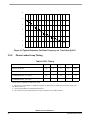
Table 3-10 Reset, Stop, Wait, Mode Select, and Interrupt Timing1, 3
Operating Conditions: VSS = VSSA = 0 V, VDD = VDDA = 3.0–3.6 V, TA = –40° to +85°C, CL ≤ 50pF
Characteristic
Symbol
Min
Max
Unit
RESET Assertion to Address, Data and Control Signals High
Impedance
tRAZ
—
21
ns
Minimum RESET Assertion Duration2
OMR Bit 6 = 0
OMR Bit 6 = 1
tRA
275,000T
128T
—
—
ns
ns
RESET De-assertion to First External Address Output
tRDA
33T
34T
ns
Edge-sensitive Interrupt Request Width
tIRW
1.5T
—
ns
1. In the formulas, T = clock cycle. For an operating frequency of 80MHz, T = 12.5ns.
2. Circuit stabilization delay is required during reset when using an external clock or crystal oscillator in two cases:
• After power-on reset
• When recovering from Stop state
3. Parameters listed are guaranteed by design.
General
Purpose
I/O Pin
tIG
IRQA
b) General Purpose I/O
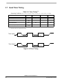
Figure 3-9 External Level-Sensitive Interrupt Timing
56F802 Technical Data, Rev. 9
Freescale Semiconductor
25