1
IBM
PowerPC 403GB
User’s Manual
Ver 0.57, 24Mar95
IBM Confidential
First Edition (March 1995)
This edition of IBM PowerPC 403GB User’s Manual applies to the IBM PPC403GB-KA 32-bit
embedded controller, as well as to subsequent IBM PowerPC 400 embedded controllers until otherwise indicated in new versions or technical newsletters.
The following paragraph does not apply to the United Kingdom or any country where such provisions are inconsistent with local law: INTERNATIONAL BUSINESS MACHINES CORPORATION PROVIDES THIS MANUAL “AS IS” WITHOUT WARRANTY OF ANY KIND, EITHER
EXPRESSED OR IMPLIED, INCLUDING, BUT NOT LIMITED TO, THE IMPLIED WARRANTIES OF
MERCHANTABILITY AND FITNESS FOR A PARTICULAR PURPOSE. Some states do not allow
disclaimer of express or implied warranties in certain transactions; therefore, this statement
may not apply to you.
IBM does not warrant that the products in this publication, whether individually or as one or more
groups, will meet your requirements or that the publication or the accompanying product descriptions
are error-free.
This publication could contain technical inaccuracies or typographical errors. Changes are periodically
made to the information herein; these changes will be incorporated in new editions of the publication.
IBM may make improvements and/or changes in the product(s) and/or program(s) described in this
publication at any time.
It is possible that this publication may contain references to, or information about, IBM products
(machines and programs), programming, or services that are not announced in your country. Such references or information must not be construed to mean that IBM intends to announce such IBM products, programming, or services in your country. Any reference to an IBM licensed program in this
publication is not intended to state or imply that you can use only IBM’s licensed program. You can use
any functionally equivalent program instead.
No part of this publication may be reproduced or distributed in any form or by any means, or stored in a
data base or retrieval system, without the written permission of IBM.
Requests for copies of this publication and for technical information about IBM products should be
made to your IBM Authorized Dealer or your IBM Marketing Representative.
Address comments about this publication to:
IBM Corporation
Department H83A
P.O. Box 12195
Research Triangle Park, NC 27709
IBM may use or distribute whatever information you supply in any way it believes appropriate without
incurring any obligation to you.
Copyright International Business Machines Corporation 1993, 1994. All rights reserved.
Printed in the United States of America.
4321
Notice to U.S. Government Users–Documentation Related to Restricted Rights –Use, duplication, or
disclosure is subject to restrictions set forth in GSA ADP Schedule Contract with IBM Corporation.
IBM Confidential
Ver 0.57, 24Mar95
Patents and Trademarks
IBM may have patents or pending patent applications covering the subject matter in this publication.
The furnishing of this publication does not give you any license to these patents. You can send license
inquiries, in writing, to the IBM Director of Licensing, IBM Corporation, 208 Harbor Drive, Stamford, CT
06904, United States of America.
The following terms are trademarks of IBM Corporation:
PPC403GB
IBM
PowerPC
PowerPC Architecture
PowerPC Embedded Controllers
RISCWatch
RISCTrace
OS Open
The following terms are trademarks of other companies:
UNIX is a registered trademark in the United States and other countries licensed exclusively
through X/Open Company Limited.
Windows is a trademark of Microsoft Corporation.
Other terms which are trademarks are the property of their respective owners.
Ver 0.57, 24Mar95
IBM Confidential
IBM Confidential
Ver 0.57, 24Mar95
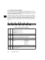
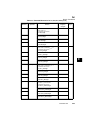
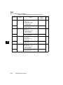
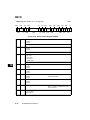
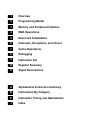
Contents
1Contents
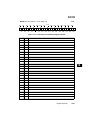
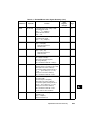
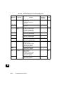
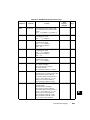
About This Book ............................................................................ xxiii
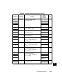
Overview ........................................................................................... 1-1
PPC403GB Overview .......................................................................................................... 1-1
PowerPC Architecture .......................................................................................................... 1-2
The PPC403GB as a PowerPC Implementation ............................................................. 1-2
PPC403GB Features ........................................................................................................... 1-3
RISC Core ....................................................................................................................... 1-4
Execution Unit (EXU) ................................................................................................. 1-4
Instruction Cache Unit (ICU) ...................................................................................... 1-5
Data Cache Unit (DCU) .............................................................................................. 1-6
Bus Interface Unit (BIU) .................................................................................................. 1-6
External Interfaces to DRAM, SRAM, ROM, and I/O ................................................. 1-6
RISC Core Interface ................................................................................................... 1-7
DMA Interface ............................................................................................................ 1-7
External Bus Master Interface .................................................................................... 1-7
DMA Controller ................................................................................................................ 1-8
Asynchronous Interrupt Controller .................................................................................. 1-9
Debug Port ...................................................................................................................... 1-9
Data Types ...................................................................................................................... 1-9
Register Set Summary .................................................................................................. 1-10
General Purpose Registers ...................................................................................... 1-10
Special Purpose Registers (SPR) ............................................................................ 1-10
Machine State Register ............................................................................................ 1-10
Condition Register .................................................................................................... 1-10
Device Control Registers .......................................................................................... 1-10
Addressing Modes ........................................................................................................ 1-10
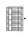
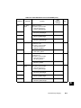
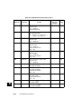
Programming Model ........................................................................ 2-1
Chapter Overview ................................................................................................................ 2-1
Memory Organization and Addressing ................................................................................. 2-2
Double-Mapping .............................................................................................................. 2-2
Supported Memory .......................................................................................................... 2-3
Memory Map -- Cacheability Regions ............................................................................. 2-3
PPC403GB Register Set ...................................................................................................... 2-5
General Purpose Registers ............................................................................................. 2-5
Special Purpose Registers .............................................................................................. 2-5
Count Register (CTR) ................................................................................................. 2-6
Link Register (LR) ...................................................................................................... 2-7
Processor Version Register (PVR) ............................................................................. 2-8
Special Purpose Register General (SPRG0-SPRG3) ................................................ 2-8
Fixed Point Exception Register (XER) ....................................................................... 2-9
Condition Register (CR) ................................................................................................ 2-11
CR Fields after Compare Instructions ...................................................................... 2-12
Ver 0.57, 24Mar95
IBM Confidential
Contents
v
The CR0 Field ..........................................................................................................
Machine State Register ................................................................................................
Device Control Registers ..............................................................................................
JTAG Accessible Registers ..........................................................................................
Data Types and Alignment ................................................................................................
Alignment for Data Movement Instructions ...................................................................
Alignment for Cache Control Instructions .....................................................................
Little Endian Mode .............................................................................................................
Non-processor Memory Access in Little-Endian ...........................................................
Control of Endian Mode ................................................................................................
Instruction Queue ..............................................................................................................
Data and Instruction Caches .............................................................................................
Instruction Cache ..........................................................................................................
Data Cache ...................................................................................................................
Branching Control ..............................................................................................................
AA Field on Unconditional Branches ............................................................................
AA Field on Conditional Branches ................................................................................
BI Field on Conditional Branches .................................................................................
BO Field on Conditional Branches ................................................................................
Branch Prediction .........................................................................................................
Speculative Fetching .........................................................................................................
Architectural Overview of Speculative Accesses ..........................................................
Speculative Accesses on PPC403GB ..........................................................................
Pre-Fetch Distance from an Unresolved Branch .....................................................
Pre-Fetch of Branch to Count / Branch to Link ........................................................
Fetching Past an Interrupt-Causing / Returning Instruction .....................................
Fetching Past tw or twi Instructions .........................................................................
Fetching Past an Unconditional Branch ...................................................................
Suggested Location of Memory-Mapped Hardware ................................................
Summary ......................................................................................................................
Memory Protection ............................................................................................................
Application to Data Cache Instructions .........................................................................
Application to String Instructions ..................................................................................
Protection Bound Lower Register (PBL1-PBL2) ...........................................................
Protection Bound Upper Register (PBU1-PBU2) ..........................................................
Privileged Mode Operation ................................................................................................
Background and Terminology .......................................................................................
MSR Bits and Exception Handling ................................................................................
Privileged Instructions ...................................................................................................
Privileged SPRs ............................................................................................................
Privileged DCRs ...........................................................................................................
Operation with an External Debugger ...........................................................................
Context, Execution, and Storage Synchronization ............................................................
Context Synchronization ...............................................................................................
Execution Synchronization ...........................................................................................
Storage Synchronization ...............................................................................................
Interrupts and Exceptions ..................................................................................................
vi
PPC403GB User’s Manual
IBM Confidential
2-12
2-13
2-14
2-14
2-14
2-16
2-16
2-17
2-21
2-22
2-23
2-24
2-24
2-25
2-26
2-26
2-26
2-26
2-26
2-28
2-29
2-29
2-30
2-30
2-30
2-31
2-31
2-32
2-32
2-32
2-33
2-34
2-35
2-35
2-36
2-36
2-36
2-36
2-37
2-37
2-38
2-38
2-38
2-38
2-41
2-42
2-43
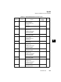
Ver 0.57, 24Mar95
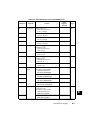
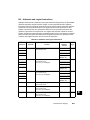
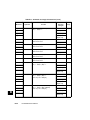
Exception Handling ....................................................................................................... 2-46
Synchronous Exception Handling ............................................................................ 2-46
Critical Interrupt Handling ......................................................................................... 2-46
Instruction Machine Check Handling ........................................................................ 2-46
Data Machine Check Handling ................................................................................. 2-48
Instruction Set Summary .................................................................................................... 2-49
Instructions Specific to PowerPC Embedded Controller ............................................... 2-50
Data Movement Instructions ......................................................................................... 2-50
Arithmetic and Logical Instructions ............................................................................... 2-51
Comparison Instructions ............................................................................................... 2-52
Branch Instructions ....................................................................................................... 2-52
Condition Register Logical Instructions ......................................................................... 2-52
Rotate and Shift Instructions ......................................................................................... 2-53
Cache Control Instructions ............................................................................................ 2-53
Interrupt Control Instructions ......................................................................................... 2-54
Processor Management Instructions ............................................................................. 2-54
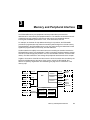
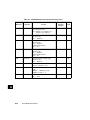
Memory and Peripheral Interface ................................................... 3-1
Memory Interface Signals .................................................................................................... 3-2
Access Priorities .................................................................................................................. 3-3
Memory Banks Supported ................................................................................................... 3-3
Attachment to the Bus .......................................................................................................... 3-4
Bus Width after Reset ..................................................................................................... 3-4
Alternative Bus Attachment ............................................................................................. 3-5
Address Bit Usage ............................................................................................................... 3-6
Cacheability ..................................................................................................................... 3-7
SRAM / DRAM Addresses .............................................................................................. 3-8
External Memory Location .............................................................................................. 3-9
The SRAM/ROM Interface ................................................................................................. 3-10
Signals .......................................................................................................................... 3-10
SRAM Read Example .............................................................................................. 3-13
SRAM Write Example ............................................................................................... 3-14
WBE Signal Usage ................................................................................................... 3-15
Device-Paced Transfers ................................................................................................ 3-15
SRAM Device-Paced Read Example ....................................................................... 3-16
SRAM Device-Paced Write Example ....................................................................... 3-17
SRAM/ROM Burst Mode ............................................................................................... 3-18
SRAM Burst Read Example ..................................................................................... 3-19
SRAM Burst Write Example ..................................................................................... 3-20
Bank Registers for SRAM Devices ............................................................................... 3-21
The DRAM Interface .......................................................................................................... 3-26
Signals .......................................................................................................................... 3-26
DRAM Read Example .............................................................................................. 3-28
DRAM Write Example .............................................................................................. 3-29
DRAM Page Mode Read Example ........................................................................... 3-30
DRAM Page Mode Write Example ........................................................................... 3-32
DRAM CAS Before RAS Refresh Example .............................................................. 3-34
Bank Registers for DRAM Devices ............................................................................... 3-35
Ver 0.57, 24Mar95
IBM Confidential
Contents
vii
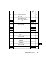
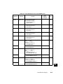
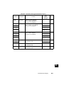
Alternate Refresh Mode ................................................................................................
Immediate Refresh ...................................................................................................
Self Refresh Mode ...................................................................................................
Example of DRAM Connection .....................................................................................
Note about SIMMs ...................................................................................................
Address Bus Multiplex for DRAM .................................................................................
External Bus Master Interface ...........................................................................................
External Bus Arbitration ................................................................................................
DRAM Accesses by the External Bus Master ...............................................................
External Master Single Transfers .............................................................................
External Master Burst Transfers ..............................................................................
3-41
3-41
3-41
3-43
3-43
3-44
3-48
3-49
3-51
3-52
3-54
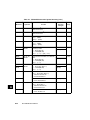
DMA Operations ............................................................................... 4-1
Overview .............................................................................................................................. 4-1
DMA Operations .................................................................................................................. 4-3
DMA Signals ................................................................................................................... 4-3
Buffered Mode Transfers ................................................................................................ 4-4
Buffered Transfer from Memory to Peripheral ........................................................... 4-6
Buffered Transfer from Peripheral to Memory ........................................................... 4-9
Fly-By Mode Transfers ................................................................................................. 4-10
Fly-By Burst .................................................................................................................. 4-14
Fly-By Burst, Memory to Peripheral ......................................................................... 4-16
Fly-By Burst, Peripheral to Memory ......................................................................... 4-18
Memory-to-Memory Mode Transfers ............................................................................ 4-19
Memory-to-Memory Transfers Initiated by Software ................................................ 4-19
Device-Paced Memory-to-Memory Transfers .......................................................... 4-21
Memory-to-Memory Line Burst Mode ........................................................................... 4-22
Packing and Unpacking of Data ................................................................................... 4-23
Chained Operations ...................................................................................................... 4-23
Chaining Example -- Quick Start of Transfer ........................................................... 4-24
Chaining Example -- No Setup Race ....................................................................... 4-25
DMA Transfer Priorities ................................................................................................ 4-26
Interrupts ....................................................................................................................... 4-27
Errors ............................................................................................................................ 4-28
DMA Registers .................................................................................................................. 4-29
DMA Channel Control Register (DMACR0-DMACR1) ................................................. 4-29
DMA Status Register (DMASR) .................................................................................... 4-32
DMA Destination Address Register (DMADA0-DMADA1) ............................................ 4-34
DMA Source/Chained Address Register (DMASA0-DMASA1) .................................... 4-34
DMA Count Register (DMACT0-DMACT1) ................................................................... 4-35
DMA Chained Count Register (DMACC0-DMACC1) ................................................... 4-36
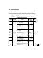
Reset and Initialization .................................................................... 5-1
Core, Chip, and System Resets ..........................................................................................
Processor State After Reset ................................................................................................
Register Contents After A Reset .........................................................................................
DRAM Controller Behavior During Reset ............................................................................
Initial Processor Sequencing ...............................................................................................
viii
PPC403GB User’s Manual
IBM Confidential
5-1
5-2
5-2
5-5
5-6
Ver 0.57, 24Mar95
Initialization Requirements ................................................................................................... 5-6
Notes on Bank Register Initialization .............................................................................. 5-7
Initialization Code Example ............................................................................................. 5-7
Interrupts, Exceptions, and Timers ................................................ 6-1
Interrupt Registers ............................................................................................................... 6-2
Machine State Register (MSR) ....................................................................................... 6-2
Save/Restore Register 0 and 1 (SRR0 - SRR1) ............................................................. 6-4
Save/Restore Register 2 and 3 (SRR2 - SRR3) ............................................................. 6-5
Exception Vector Prefix Register (EVPR) ....................................................................... 6-7
External Interrupt Enable Register (EXIER) .................................................................... 6-8
External Interrupt Status Register (EXISR) ..................................................................... 6-9
Input/Output Configuration Register (IOCR) ................................................................. 6-11
Exception Syndrome Register (ESR) ............................................................................ 6-12
Bus Error Syndrome Register (BESR) .......................................................................... 6-13
Bus Error Address Register (BEAR) ............................................................................. 6-14
Data Exception Address Register (DEAR) .................................................................... 6-15
Exception Causes and Machine State ............................................................................... 6-15
Reset Exceptions .......................................................................................................... 6-15
Core Reset ............................................................................................................... 6-16
Chip Reset ................................................................................................................ 6-16
System Reset ........................................................................................................... 6-16
Critical Interrupt Pin Exception ...................................................................................... 6-17
Machine Check Exceptions ........................................................................................... 6-18
Protection Exception ..................................................................................................... 6-19
External Interrupt Exception .......................................................................................... 6-20
Alignment Error ............................................................................................................. 6-21
Program Exceptions ...................................................................................................... 6-22
System Call ................................................................................................................... 6-22
Programmable Interval Timer ........................................................................................ 6-23
Fixed Interval Timer ...................................................................................................... 6-24
Watchdog Timer ............................................................................................................ 6-24
Debug Exception ........................................................................................................... 6-25
Timer Architecture .............................................................................................................. 6-27
Timer Clocks ................................................................................................................. 6-27
Time Base (TBHI and TBLO) ........................................................................................ 6-28
Comparison with PowerPC Architecture Time Base ................................................ 6-28
Programmable Interval Timer (PIT) ............................................................................... 6-30
Fixed Interval Timer (FIT) .............................................................................................. 6-31
Watch Dog Timer (WDT) ............................................................................................... 6-32
Timer Status Register (TSR) ......................................................................................... 6-34
Timer Control Register (TCR) ....................................................................................... 6-34
Cache Operations ............................................................................ 7-1
Cache Debugging Features ................................................................................................. 7-1
Instruction Cache Unit .......................................................................................................... 7-1
Instruction Cache Operations .......................................................................................... 7-2
Instruction Cache Cacheability Register (ICCR) ............................................................. 7-4
Ver 0.57, 24Mar95
IBM Confidential
Contents
ix
ICU Instructions .............................................................................................................. 7-5
ICU Debugging ............................................................................................................... 7-6
Data Cache Unit .................................................................................................................. 7-6
Data Cache Operations .................................................................................................. 7-7
Data Cache Cacheability Register (DCCR) .................................................................... 7-8
DCU Instructions ............................................................................................................. 7-9
DCU Debugging ............................................................................................................ 7-10
Debugging ........................................................................................ 8-1
Development Tool Support .................................................................................................. 8-1
Debug Modes ...................................................................................................................... 8-1
Internal Debug Mode ...................................................................................................... 8-2
External Debug Mode ..................................................................................................... 8-2
Processor Control ................................................................................................................ 8-2
Processor Status ................................................................................................................. 8-3
Debug Events ...................................................................................................................... 8-4
Debug Flow ......................................................................................................................... 8-4
Debug Registers .................................................................................................................. 8-5
Debug Control Register (DBCR) ..................................................................................... 8-5
Debug Status Register (DBSR) ...................................................................................... 8-8
Data Address Compare Registers (DAC1-DAC2) .......................................................... 8-9
Instruction Address Compare (IAC1-IAC2) ................................................................... 8-10
Debug Interfaces ............................................................................................................... 8-10
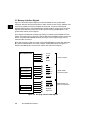
IEEE 1149.1 Test Access Port (JTAG) ......................................................................... 8-10
JTAG Connector ...................................................................................................... 8-11
JTAG Instructions .................................................................................................... 8-12
JTAG Boundary Scan Chain .................................................................................... 8-13
Instruction Set .................................................................................. 9-1
Instruction Formats .............................................................................................................. 9-1
Instruction Fields ................................................................................................................. 9-2
Pseudocode ......................................................................................................................... 9-4
Register Usage .................................................................................................................... 9-6
add ....................................................................................................................................... 9-7
addc ..................................................................................................................................... 9-8
adde ..................................................................................................................................... 9-9
addi .................................................................................................................................... 9-10
addic .................................................................................................................................. 9-11
addic. ................................................................................................................................. 9-12
addis .................................................................................................................................. 9-13
addme ................................................................................................................................ 9-14
addze ................................................................................................................................. 9-15
and ..................................................................................................................................... 9-16
andc ................................................................................................................................... 9-17
andi. ................................................................................................................................... 9-18
andis. ................................................................................................................................. 9-19
b ......................................................................................................................................... 9-20
bc ....................................................................................................................................... 9-21
x
PPC403GB User’s Manual
IBM Confidential
Ver 0.57, 24Mar95
bcctr ................................................................................................................................... 9-28
bclr ..................................................................................................................................... 9-32
cmp .................................................................................................................................... 9-37
cmpi ................................................................................................................................... 9-38
cmpl ................................................................................................................................... 9-39
cmpli ................................................................................................................................... 9-40
cntlzw ................................................................................................................................. 9-41
crand .................................................................................................................................. 9-42
crandc ................................................................................................................................ 9-43
creqv .................................................................................................................................. 9-44
crnand ................................................................................................................................ 9-45
crnor ................................................................................................................................... 9-46
cror ..................................................................................................................................... 9-47
crorc ................................................................................................................................... 9-48
crxor ................................................................................................................................... 9-49
dcbf .................................................................................................................................... 9-50
dcbi .................................................................................................................................... 9-51
dcbst .................................................................................................................................. 9-52
dcbt .................................................................................................................................... 9-53
dcbtst ................................................................................................................................. 9-54
dcbz ................................................................................................................................... 9-55
dccci ................................................................................................................................... 9-57
dcread ................................................................................................................................ 9-58
divw .................................................................................................................................... 9-60
divwu .................................................................................................................................. 9-61
eieio ................................................................................................................................... 9-62
eqv ..................................................................................................................................... 9-63
extsb .................................................................................................................................. 9-64
extsh .................................................................................................................................. 9-65
icbi ...................................................................................................................................... 9-66
icbt ..................................................................................................................................... 9-67
iccci .................................................................................................................................... 9-68
icread ................................................................................................................................. 9-69
isync ................................................................................................................................... 9-71
lbz ...................................................................................................................................... 9-72
lbzu .................................................................................................................................... 9-73
lbzux ................................................................................................................................... 9-74
lbzx ..................................................................................................................................... 9-75
lha ...................................................................................................................................... 9-76
lhau .................................................................................................................................... 9-77
lhaux .................................................................................................................................. 9-78
lhax .................................................................................................................................... 9-79
lhbrx ................................................................................................................................... 9-80
lhz ...................................................................................................................................... 9-81
lhzu .................................................................................................................................... 9-82
lhzux ................................................................................................................................... 9-83
lhzx ..................................................................................................................................... 9-84
Ver 0.57, 24Mar95
IBM Confidential
Contents
xi
lmw .................................................................................................................................... 9-85
lswi ..................................................................................................................................... 9-86
lswx .................................................................................................................................... 9-88
lwarx .................................................................................................................................. 9-90
lwbrx .................................................................................................................................. 9-92
lwz ..................................................................................................................................... 9-93
lwzu ................................................................................................................................... 9-94
lwzux .................................................................................................................................. 9-95
lwzx .................................................................................................................................... 9-96
mcrf .................................................................................................................................... 9-97
mcrxr .................................................................................................................................. 9-98
mfcr .................................................................................................................................... 9-99
mfdcr ................................................................................................................................ 9-100
mfmsr ............................................................................................................................... 9-102
mfspr ................................................................................................................................ 9-103
mtcrf ................................................................................................................................. 9-105
mtdcr ................................................................................................................................ 9-107
mtmsr ............................................................................................................................... 9-109
mtspr ................................................................................................................................ 9-110
mulhw .............................................................................................................................. 9-112
mulhwu ............................................................................................................................ 9-113
mulli ................................................................................................................................. 9-114
mullw ............................................................................................................................... 9-115
nand ................................................................................................................................. 9-116
neg ................................................................................................................................... 9-117
nor ................................................................................................................................... 9-118
or ..................................................................................................................................... 9-119
orc .................................................................................................................................... 9-120
ori ..................................................................................................................................... 9-121
oris ................................................................................................................................... 9-122
rfci .................................................................................................................................... 9-123
rfi ...................................................................................................................................... 9-124
rlwimi ............................................................................................................................... 9-125
rlwinm .............................................................................................................................. 9-126
rlwnm ............................................................................................................................... 9-129
sc ..................................................................................................................................... 9-130
slw ................................................................................................................................... 9-131
sraw ................................................................................................................................. 9-132
srawi ................................................................................................................................ 9-133
srw ................................................................................................................................... 9-134
stb .................................................................................................................................... 9-135
stbu .................................................................................................................................. 9-136
stbux ................................................................................................................................ 9-137
stbx .................................................................................................................................. 9-138
sth .................................................................................................................................... 9-139
sthbrx ............................................................................................................................... 9-140
sthu .................................................................................................................................. 9-141
xii
PPC403GB User’s Manual
IBM Confidential
Ver 0.57, 24Mar95
sthux ................................................................................................................................ 9-142
sthx .................................................................................................................................. 9-143
stmw ................................................................................................................................. 9-144
stswi ................................................................................................................................. 9-145
stswx ................................................................................................................................ 9-146
stw .................................................................................................................................... 9-148
stwbrx ............................................................................................................................... 9-149
stwcx. ............................................................................................................................... 9-150
stwu .................................................................................................................................. 9-152
stwux ................................................................................................................................ 9-153
stwx .................................................................................................................................. 9-154
subf .................................................................................................................................. 9-155
subfc ................................................................................................................................ 9-156
subfe ................................................................................................................................ 9-157
subfic ................................................................................................................................ 9-158
subfme ............................................................................................................................. 9-159
subfze .............................................................................................................................. 9-160
sync .................................................................................................................................. 9-161
tw ..................................................................................................................................... 9-162
twi ..................................................................................................................................... 9-164
wrtee ................................................................................................................................ 9-166
wrteei ............................................................................................................................... 9-167
xor .................................................................................................................................... 9-168
xori ................................................................................................................................... 9-169
xoris ................................................................................................................................. 9-170
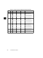
Register Summary ......................................................................... 10-1
Reserved Registers ........................................................................................................... 10-1
Reserved Fields ................................................................................................................. 10-1
General Purpose Register Numbering ............................................................................... 10-1
Machine State Register and Condition Register Numbering ............................................. 10-2
Device Control Register Numbering .................................................................................. 10-2
Special Purpose Register Numbering ................................................................................ 10-3
Signal Descriptions ....................................................................... 11-1
Alphabetical Instruction Summary ................................................ A-1
Instruction Set and Extended Mnemonics – Alphabetical ................................................... A-1
Instructions By Category ............................................................... B-1
Instruction Set Summary – Categories ............................................................................... B-1
Instructions Specific to PowerPC Embedded Controllers ................................................... B-1
Privileged Instructions ......................................................................................................... B-3
Assembler Extended Mnemonics ....................................................................................... B-5
Data Movement Instructions ............................................................................................. B-28
Arithmetic and Logical Instructions ................................................................................... B-33
Condition Register Logical Instructions ............................................................................. B-38
Branch Instructions ........................................................................................................... B-39
Ver 0.57, 24Mar95
IBM Confidential
Contents
xiii
Comparison Instructions .................................................................................................... B-40
Rotate and Shift Instructions ............................................................................................. B-41
Cache Control Instructions ................................................................................................ B-43
Interrupt Control Instructions ............................................................................................. B-44
Processor Management Instructions ................................................................................. B-45
Instruction Timing and Optimization ............................................. C-1
Background Information ..................................................................................................... C-1
Superscalar Operation ................................................................................................... C-1
Folding Defined .............................................................................................................. C-1
Branch Folding ............................................................................................................... C-2
Coding Guidelines .............................................................................................................. C-3
Condition Register Bits for Boolean Variables ............................................................... C-3
CR Logical Instructions for Compound Branches .......................................................... C-3
Floating Point Emulation ................................................................................................ C-3
Data Cache Usage ........................................................................................................ C-4
Instruction Cache Usage ............................................................................................... C-4
Dependency Upon CR ................................................................................................... C-4
Dependency Upon LR and CTR .................................................................................... C-5
Load Latency ................................................................................................................. C-5
Branch Prediction .......................................................................................................... C-5
Alignment ....................................................................................................................... C-6
Instruction Timings ............................................................................................................. C-7
General Rules ................................................................................................................ C-7
Branch and CR Logical Opcodes .................................................................................. C-7
Branch Prediction .......................................................................................................... C-8
String Opcodes .............................................................................................................. C-8
Data Cache Loads and Stores ....................................................................................... C-9
Instruction Cache Misses ............................................................................................... C-9
Detailed Folding Rules ..................................................................................................... C-10
Instruction Classifications for Folding .......................................................................... C-10
Instructions That Can Be Folded ................................................................................. C-11
Fold Blocking Rules For CR Logical and mcrf Instructions .......................................... C-11
Fold Blocking Rules For Branch Instructions ............................................................... C-11
Fold Blocking During Debug ........................................................................................ C-13
Index ................................................................................................... I-1
xiv
PPC403GB User’s Manual
IBM Confidential
Ver 0.57, 24Mar95
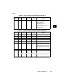
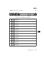
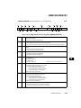
Figures
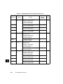
1Figures
Figure 1-1.
Figure 2-1.
Figure 2-2.
Figure 2-3.
Figure 2-4.
Figure 2-5.
Figure 2-6.
Figure 2-7.
Figure 2-8.
Figure 2-9.
Figure 2-10.
Figure 2-11.
Figure 2-12.
Figure 3-1.
Figure 3-2.
Figure 3-3.
Figure 3-4.
Figure 3-5.
Figure 3-6.
Figure 3-7.
Figure 3-8.
Figure 3-9.
Figure 3-10.
Figure 3-11.
Figure 3-12.
Figure 3-13.
Figure 3-14.
Figure 3-15.
Figure 3-16.
Figure 3-17.
Figure 3-18.
Figure 3-19.
Figure 3-20.
Figure 3-21.
Figure 3-22.
Figure 3-23.
Figure 3-24.
Figure 3-25.
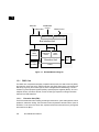
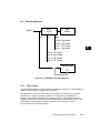
PPC403GB Block Diagram ............................................................................... 1-4
PPC403GB Address Map ................................................................................. 2-4
General Purpose Register (R0-R31) ................................................................ 2-5
Count Register (CTR) ....................................................................................... 2-6
Link Register (LR) ............................................................................................. 2-7
Processor Version Register (PVR) ................................................................... 2-8
Special Purpose Register General (SPRG0-SPRG3) ...................................... 2-9
Fixed Point Exception Register (XER) .............................................................. 2-9
Condition Register (CR) .................................................................................. 2-11
PPC403GB Data types ................................................................................... 2-15
PPC403GB Instruction Queue ........................................................................ 2-23
Protection Bound Lower Register (PBL1-PBL2) ............................................. 2-35
Protection Bound Upper Register (PBU1-PBU2) ............................................ 2-36
BIU Interfaces ................................................................................................... 3-1
Grouping of External BIU Signals ..................................................................... 3-2
Attachment of Devices of Various Widths to the PPC403GB Data Bus ........... 3-5
Usage of Address Bits ...................................................................................... 3-6
Parameter Definitions -- SRAM Single Transfer ............................................. 3-11
Parameter Definitions -- SRAM Burst Mode ................................................... 3-12
Timing Diagram -- SRAM Read ...................................................................... 3-13
Timing Diagram -- SRAM Write ...................................................................... 3-14
Timing Diagram -- SRAM Read Extended with Ready ................................... 3-16
Timing Diagram -- SRAM Write Extended with Ready ................................... 3-17
SRAM/ROM Burst Read Request ................................................................... 3-19
SRAM/ROM Burst Write Request with Wait and Hold .................................... 3-20
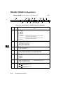
Bank Registers - SRAM Configuration (BR0-BR3, BR6-BR7) ........................ 3-21
Parameter Definitions -- DRAM ...................................................................... 3-27
DRAM Single Transfer Read .......................................................................... 3-28
DRAM Single Transfer Write .......................................................................... 3-29
DRAM 3-2-2-2 Page Mode Read .................................................................... 3-30
DRAM 2-1-1-1 Page Mode Read .................................................................... 3-31
DRAM 3-2-2-2 Page Mode Write .................................................................... 3-32
DRAM 2-1-1-1 Page Mode Write .................................................................... 3-33
DRAM Refresh Timing, CAS Before RAS, 1 Bank ......................................... 3-34
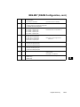
Bank Registers - DRAM Configuration (BR6-BR7) ......................................... 3-35
Example of DRAM Connection ....................................................................... 3-43
Sample PPC403GB / External Bus Master System ........................................ 3-48
HoldReq/HoldAck Bus Arbitration ................................................................... 3-50
Ver 0.57, 24Mar95
IBM Confidential
Figures
xv
Figure 3-26.
Figure 3-27.
Figure 4-1.
Figure 4-2.
Figure 4-3.
Figure 4-4.
Figure 4-5.
Figure 4-6.
Figure 4-7.
Figure 4-8.
Figure 4-9.
Figure 4-10.
Figure 4-11.
Figure 4-12.
Figure 4-13.
Figure 4-14.
Figure 4-15.
Figure 4-16.
Figure 4-17.
Figure 4-18.
Figure 4-19.
Figure 4-20.
Figure 4-21.
Figure 4-22.
Figure 6-1.
Figure 6-2.
Figure 6-3.
Figure 6-4.
Figure 6-5.
Figure 6-6.
Figure 6-7.
Figure 6-8.
Figure 6-9.
Figure 6-10.
Figure 6-11.
Figure 6-12.
Figure 6-13.
Figure 6-14.
Figure 6-15.
Figure 6-16.
xvi
External Bus Master Read Using the Internal DRAM Controller .................... 3-53
Burst Write to 3-2-2-2 Page Mode DRAM ...................................................... 3-55
PPC403GB DMA Controller Interfaces ............................................................ 4-1
DMA Controller Block Diagram ........................................................................ 4-2
Overview of Buffered Mode Transfers .............................................................. 4-4
DMACR Setting for Buffered DRAM Read, Peripheral Write ........................... 4-6
Buffered Mode Transfer from a 32-bit 2-1-1-1 DRAM to a 32-bit Peripheral .... 4-8
Buffered Mode Transfer from a 32-bit Peripheral to a 32-bit DRAM ................ 4-9
Overview of Fly-by Mode DMA Transfer ........................................................ 4-10
DMACR Setting for Fly-By Memory Read, Peripheral Write .......................... 4-11
Fly-By Transfer from 3-cycle DRAM to a 32-bit Peripheral ............................ 4-12
DMACR Setting for Fly-By Burst, Peripheral Write ........................................ 4-16
DMA Fly-by Burst; 2-1-1-1 DRAM; 2 Transfers .............................................. 4-17
DMA Fly-by Burst; 3-2-2-2 DRAM; Single Transfers ...................................... 4-18
DMACR Setting for Memory-to-Memory Transfer .......................................... 4-19
Overview of Memory to Memory Mode DMA Transfer ................................... 4-20
Memory-to-Memory Line Burst, 2-1-1-1 DRAM .............................................. 4-22
DMA Transfer Priorities .................................................................................. 4-26
DMA Channel Control Registers (DMACR0-DMACR1) ................................. 4-29
DMA Status Register (DMASR) ..................................................................... 4-32
DMA Destination Address Registers (DMADA0-DMADA1) ........................... 4-34
DMA Source Address Registers (DMASA0-DMASA1) .................................. 4-35
DMA Count Registers (DMACT0-DMACT1) .................................................. 4-35
DMA Chained Count Registers (DMACC0-DMACC1) ................................... 4-36
Machine State Register (MSR) ......................................................................... 6-3
Save / Restore Register 0 (SRR0) .................................................................. 6-4
Save / Restore Register 1 (SRR1) .................................................................. 6-4
Save / Restore Register 2 (SRR2) .................................................................. 6-6
Save / Restore Register 3 (SRR3) .................................................................. 6-6
Exception Vector Prefix Register (EVPR) ........................................................ 6-7
External Interrupt Enable Register (EXIER) ..................................................... 6-8
External Interrupt Status Register (EXISR) ...................................................... 6-9
Input/Output Configuration Register (IOCR) .................................................. 6-11
Exception Syndrome Register (ESR) ............................................................. 6-12
Bus Error Syndrome Register (BESR) ........................................................... 6-14
Bus Address Error Register (BEAR) .............................................................. 6-15
Data Exception Address Register (DEAR) ..................................................... 6-15
PPC403GB Timer Block Diagram .................................................................. 6-27
Time Base High Register (TBHI) .................................................................... 6-28
Time Base Low Register (TBLO) ................................................................... 6-28
PPC403GB User’s Manual
IBM Confidential
Ver 0.57, 24Mar95
Figure 6-17.
Figure 6-18.
Figure 6-19.
Figure 7-1.
Figure 7-2.
Figure 7-3.
Figure 7-4.
Figure 7-5.
Figure 7-6.
Figure 7-7.
Figure 8-1.
Figure 8-2.
Figure 8-3.
Figure 8-4.
Figure 8-5.
Figure 10-1.
Figure 10-2.
Figure 10-3.
Figure 10-4.
Figure 10-5.
Figure 10-6.
Figure 10-7.
Figure 10-8.
Figure 10-9.
Figure 10-10.
Figure 10-11.
Figure 10-12.
Figure 10-13.
Figure 10-14.
Figure 10-15.
Figure 10-16.
Figure 10-17.
Figure 10-18.
Figure 10-19.
Figure 10-20.
Figure 10-21.
Figure 10-22.
Figure 10-23.
Figure 10-24.
Figure 10-25.
Programmable Interval Timer (PIT) ................................................................ 6-31
Timer Status Register (TSR) .......................................................................... 6-34
Timer Control Register (TCR) ......................................................................... 6-35
Cache Debug Control Register (CDBCR) ......................................................... 7-1
Instruction Cache Organization ........................................................................ 7-2
Instruction Flow ................................................................................................. 7-3
Instruction Cache Cacheability Register (ICCR) ............................................... 7-4
Instruction Cache Debug Data Register (ICDBDR) .......................................... 7-6
Data Cache Organization ................................................................................. 7-7
Data Cache Cacheability Register (DCCR) ...................................................... 7-8
Debug Control Register (DBCR) ....................................................................... 8-6
Debug Status Register (DBSR) ........................................................................ 8-8
Data Address Compare Registers (DAC1-DAC2) .......................................... 8-10
Instruction Address Compare (IAC1-IAC2) ..................................................... 8-10
JTAG Connector (top view) Physical Layout .................................................. 8-11
Bus Address Error Register (BEAR) ............................................................... 10-6
Bus Error Syndrome Register (BESR) ............................................................ 10-7
Bank Registers - SRAM Configuration (BR0-BR3, BR6-BR7) ........................ 10-8
Bank Registers - DRAM Configuration (BR6-BR7) ....................................... 10-10
Cache Debug Control Register (CDBCR) ..................................................... 10-12
Condition Register (CR) ................................................................................ 10-13
Count Register (CTR) ................................................................................... 10-14
Data Address Compare Registers (DAC1-DAC2) ........................................ 10-15
Debug Control Register (DBCR) ................................................................... 10-16
Debug Status Register (DBSR) .................................................................... 10-19
Data Cache Cacheability Register (DCCR) .................................................. 10-21
Data Exception Address Register (DEAR) ................................................... 10-23
DMA Chained Count Registers (DMACC0-DMACC1) .................................. 10-24
DMA Channel Control Registers (DMACR0-DMACR1) ................................ 10-25
DMA Count Registers (DMACT0-DMACT1) ................................................. 10-27
DMA Destination Address Registers (DMADA0-DMADA1) .......................... 10-28
DMA Source Address Registers (DMASA0-DMASA1) ................................. 10-29
DMA Status Register (DMASR) .................................................................... 10-30
Exception Syndrome Register (ESR) ........................................................... 10-32
Exception Vector Prefix Register (EVPR) ..................................................... 10-33
External Interrupt Enable Register (EXIER) ................................................. 10-34
External Interrupt Status Register (EXISR) .................................................. 10-35
General Purpose Register (R0-R31) ............................................................ 10-36
Instruction Address Compare (IAC1-IAC2) ................................................... 10-37
Instruction Cache Cacheability Register (ICCR) ........................................... 10-38
Ver 0.57, 24Mar95
IBM Confidential
Figures
xvii
Figure 10-26.
Figure 10-27.
Figure 10-28.
Figure 10-29.
Figure 10-30.
Figure 10-31.
Figure 10-32.
Figure 10-33.
Figure 10-34.
Figure 10-35.
Figure 10-36.
Figure 10-37.
Figure 10-38.
Figure 10-39.
Figure 10-40.
Figure 10-41.
Figure 10-42.
Figure 10-43.
xviii
Instruction Cache Debug Data Register (ICDBDR) ......................................
Input/Output Configuration Register (IOCR) ................................................
Link Register (LR) ........................................................................................
Machine State Register (MSR) .....................................................................
Protection Bound Lower Register (PBL1-PBL2) ..........................................
Protection Bound Upper Register (PBU1-PBU2) .........................................
Programmable Interval Timer (PIT) ..............................................................
Processor Version Register (PVR) ...............................................................
Special Purpose Register General (SPRG0-SPRG3) ..................................
Save / Restore Register 0 (SRR0) ..............................................................
Save / Restore Register 1 (SRR1) ..............................................................
Save / Restore Register 2 (SRR2) ..............................................................
Save / Restore Register 3 (SRR3) ..............................................................
Time Base High Register (TBHI) ..................................................................
Time Base Low Register (TBLO) .................................................................
Timer Control Register (TCR) ......................................................................
Timer Status Register (TSR) ........................................................................
Fixed Point Exception Register (XER) .........................................................
PPC403GB User’s Manual
IBM Confidential
10-40
10-41
10-43
10-44
10-46
10-47
10-48
10-49
10-50
10-51
10-52
10-54
10-55
10-57
10-58
10-59
10-60
10-61
Ver 0.57, 24Mar95
Tables
1Tables
Table 2-1.
Table 2-2.
Table 2-3.
Table 2-4.
Table 2-5.
Table 2-6.
Table 2-7.
Table 2-8.
Table 2-9.
Table 2-10.
Table 2-11.
Table 2-12.
Table 2-13.
Table 2-14.
Table 2-15.
Table 2-16.
Table 2-17.
Table 2-18.
Table 2-19.
Table 2-20.
Table 2-21.
Table 2-22.
Table 2-23.
Table 3-1.
Table 3-2.
Table 3-3.
Table 3-4.
Table 3-5.
Table 3-6.
Table 3-7.
Table 3-8.
Table 3-9.
Table 3-10.
Table 4-1.
Table 4-2.
Table 4-3.
Table 4-4.
Table 4-5.
Special Purpose Register (SPR) List ................................................................ 2-6
Device Control Register (DCR) List ................................................................ 2-14
Address Alteration in Little-Endian Mode ........................................................ 2-20
Bits of the BO Field ......................................................................................... 2-27
Conditional Branch BO Field .......................................................................... 2-27
SRAM Mapping ............................................................................................... 2-32
Handling of Dcache Instructions ..................................................................... 2-35
Privileged Instructions ..................................................................................... 2-37
PPC403GB Exception Priorities, Types and Classes ..................................... 2-44
Exception Vector Offsets ................................................................................ 2-45
ESR Usage for Program Exceptions .............................................................. 2-46
ESR Usage for Instruction Machine Checks ................................................... 2-47
PPC403GB Instruction Set Summary ............................................................. 2-49
Instructions Specific to PowerPC Embedded Controller ................................. 2-50
Data Movement Instructions ........................................................................... 2-51
Arithmetic and Logical Instructions ................................................................. 2-51
Comparison Instructions ................................................................................. 2-52
Branch Instructions ......................................................................................... 2-52
Condition Register Logical Instructions .......................................................... 2-53
Rotate and Shift Instructions ........................................................................... 2-53
Cache Control Instructions ............................................................................. 2-53
Interrupt Control Instructions .......................................................................... 2-54
Processor Management Instructions .............................................................. 2-54
SRAM And DRAM Banks Supported ................................................................ 3-4
Restrictions on Bank Starting Address ............................................................. 3-9
Usage of WBE0:WBE3 vs Bus Width ............................................................. 3-15
RR Field for Normal Refresh Mode ................................................................ 3-40
RR Field for Alternate Refresh Mode .............................................................. 3-40
Multiplexed Address Outputs .......................................................................... 3-44
DRAM Multiplex for 8 bit Bus .......................................................................... 3-45
DRAM Multiplex for 16 bit Bus ........................................................................ 3-46
DRAM Multiplex for 32 bit Bus ........................................................................ 3-47
XSize0:1 Bit Definitions .................................................................................. 3-51
Sample DMACR Settings for Buffered Transfer .............................................. 4-6
Sample DMACR Settings for Fly-By Transfer ................................................ 4-11
Sample DMACR Settings for Fly-By Burst ..................................................... 4-16
Sample DMACR Settings for Memory-to-Memory Transfer .......................... 4-19
Packing / Unpacking Support ......................................................................... 4-23
Ver 0.57, 24Mar95
IBM Confidential
Tables
xix
Table 5-1.
Table 5-2.
Table 5-3.
Table 5-4.
Table 6-1.
Table 6-2.
Table 6-3.
Table 6-4.
Table 6-5.
Table 6-6.
Table 6-7.
Table 6-8.
Table 6-9.
Table 6-10.
Table 6-11.
Table 6-12.
Table 6-13.
Table 8-1.
Table 8-2.
Table 8-3.
Table 8-4.
Table 9-1.
Table 9-2.
Table 9-3.
Table 9-4.
Table 9-5.
Table 9-6.
Table 9-7.
Table 9-8.
Table 9-9.
Table 9-10.
Table 9-11.
Table 9-12.
Table 9-13.
Table 9-14.
Table 9-15.
Table 9-16.
Table 9-17.
Table 9-18.
Table 9-19.
xx
Processor Configuration After a Reset ............................................................. 5-2
Contents of Machine State Register After Reset .............................................. 5-3
Contents of Special Purpose Registers After Reset ......................................... 5-3
Contents of Device Configuration Registers After Reset ................................. 5-4
Register Settings during Core Reset .............................................................. 6-16
Register Settings during Critical Interrupt Exceptions .................................... 6-17
Register Settings during Machine Check Exceptions ..................................... 6-18
Register Settings during Protection Violation Exceptions .............................. 6-19
Register Settings during External Interrupt Exceptions .................................. 6-21
Register Settings during Alignment Error Exceptions .................................... 6-21
Register Settings during Program Exceptions ................................................ 6-22
Register Settings during System Call Exceptions .......................................... 6-23
Register Settings during Programmable Interval Timer Exceptions ............... 6-23
Register Settings during Fixed Interval Timer Exceptions .............................. 6-24
Register Settings during Watchdog Timer Exceptions ................................... 6-25
Register Settings during Debug Exceptions ................................................... 6-26
Time Base Comparison .................................................................................. 6-30
JTAG Port Summary ...................................................................................... 8-11
JTAG Connector Signals ................................................................................ 8-12
JTAG Instructions ........................................................................................... 8-13
Boundary Scan Chain .................................................................................... 8-13
Operator Precedence ....................................................................................... 9-6
Extended Mnemonics for addi ........................................................................ 9-10
Extended Mnemonics for addic ...................................................................... 9-11
Extended Mnemonics for addic. ..................................................................... 9-12
Extended Mnemonics for addis ...................................................................... 9-13
Extended Mnemonics for bc, bca, bcl, bcla .................................................... 9-22
Extended Mnemonics for bcctr, bcctrl ............................................................ 9-29
Extended Mnemonics for bclr, bclrl ................................................................ 9-33
Extended Mnemonics for cmp ........................................................................ 9-37
Extended Mnemonics for cmpi ....................................................................... 9-38
Extended Mnemonics for cmpl ....................................................................... 9-39
Extended Mnemonics for cmpli ...................................................................... 9-40
Extended Mnemonics for creqv ...................................................................... 9-44
Extended Mnemonics for crnor ...................................................................... 9-46
Extended Mnemonics for cror ........................................................................ 9-47
Extended Mnemonics for crxor ....................................................................... 9-49
Extended Mnemonics for mfdcr .................................................................... 9-101
Extended Mnemonics for mfspr .................................................................... 9-104
Extended Mnemonics for mtcrf ..................................................................... 9-106
PPC403GB User’s Manual
IBM Confidential
Ver 0.57, 24Mar95
Table 9-20.
Table 9-21.
Table 9-22.
Table 9-23.
Table 9-24.
Table 9-25.
Table 9-26.
Table 9-27.
Table 9-28.
Table 9-29.
Table 9-30.
Table 9-31.
Table 10-1.
Table 10-2.
Table 10-3.
Table 11-1.
Table 11-2.
Table A-1.
Table B-1.
Table B-2.
Table B-3.
Table B-4.
Table B-5.
Table B-6.
Table B-7.
Table B-8.
Table B-9.
Table B-10.
Table B-11.
Table B-12.
Table B-13.
Table C-1.
Table C-2.
Table C-3.
Extended Mnemonics for mtdcr .................................................................... 9-108
Extended Mnemonics for mtspr .................................................................... 9-111
Extended Mnemonics for nor, nor. ................................................................ 9-118
Extended Mnemonics for or, or. .................................................................... 9-119
Extended Mnemonics for ori ......................................................................... 9-121
Extended Mnemonics for rlwimi, rlwimi. ........................................................ 9-125
Extended Mnemonics for rlwinm, rlwinm. ..................................................... 9-126
Extended Mnemonics for rlwnm, rlwnm. ....................................................... 9-129
Extended Mnemonics for subf, subf., subfo, subfo. ...................................... 9-155
Extended Mnemonics for subfc, subfc., subfco, subfco. ............................... 9-156
Extended Mnemonics for tw ......................................................................... 9-163
Extended Mnemonics for twi ......................................................................... 9-165
PPC403GB General Purpose Registers ......................................................... 10-1
PPC403GB Device Control Registers ............................................................ 10-2
PPC403GB Special Purpose Registers .......................................................... 10-4
PPC403GB Signal Descriptions ..................................................................... 11-1
Signals Ordered by Pin Number ..................................................................... 11-8
PPC403GB Instruction Syntax Summary ........................................................ A-2
PPC403GB Instruction Set Summary .............................................................. B-1
Instructions Specific to PowerPC Embedded Controllers ................................ B-2
Privileged Instructions ...................................................................................... B-3
Extended Mnemonics for PPC403GB ............................................................. B-5
Data Movement Instructions .......................................................................... B-28
Arithmetic and Logical Instructions ................................................................ B-33
Condition Register Logical Instructions ......................................................... B-38
Branch Instructions ........................................................................................ B-39
Comparison Instructions ................................................................................ B-40
Rotate and Shift Instructions .......................................................................... B-41
Cache Control Instructions ............................................................................ B-43
Interrupt Control Instructions ......................................................................... B-44
Processor Management Instructions ............................................................. B-45
CTR and LR Updating Instructions ................................................................ C-10
CR Updating Instructions ............................................................................... C-10
Foldable Instructions ...................................................................................... C-11
Ver 0.57, 24Mar95
IBM Confidential
Tables
xxi
xxii
PPC403GB User’s Manual
IBM Confidential
Ver 0.57, 24Mar95
About This Book
About This Book
This user’s manual provides the architectural overview, programming model, and detailed
information about the registers and the instruction set of the IBM™ PowerPC™ 403GB™
32-bit RISC embedded controller.
The PPC403GB RISC embedded controller features :
•
PowerPC Architecture™
•
Single-cycle execution for most instructions
•
Buffered, fly-by, or memory-to-memory two-channel DMA
•
Direct-connect DRAM, SRAM, ROM and I/O interfaces
•
On-chip 2KB instruction cache and 1KB copy-back data cache
•
JTAG port
•
Controller for one critical and five noncritical interrupt lines
•
Extensive development tool support
Who Should Use This Book
This book is for system hardware and software developers, and for application developers
who need to understand for the PPC403GB. The audience should understand embedded
system design, operating systems, RISC processing, and design for testability.
How to Use This Book
This book describes the PPC403GB device architecture, programming model, external
interfaces, internal registers, and instruction set. This book contains the following chapters:
Conventions
The following is a brief list of notational conventions frequently used in this manual. Also see
Section 9.2 and Section 9.3.
Active_Low
An overbar indicates an active-low signal.
0x1f
Hexadecimal numbers
0b1001
Binary numbers
FLD
A named field.
FLDb
A bit in a named field.
RA, RS, . . .
A general purpose register (GPR).
(RA)
The contents of a GPR.
Ver 0.57, 24Mar95
IBM Confidential
About This Book
xxiii
(RA)|0
The contents of a GPR or the value 0.
REGb
A bit in a named register.
REGb:b
A range of bits in a named register.
REGb,b, . . .
A list of bits, by number or name, in a named register.
REG[FLD]
A field of a named register.
CRFLD
The field in the condition register pointed to by a field of an instruction.
24s
The sign bit is replicated (sign-extended) 24 times.
xx
Bit positions which are don’t-cares.
Related Publications
The following publications contain related information:
• PowerPC 403GB Data Sheet, MPR4GBDSU-01
To obtain copies of this publication, call the IBM PowerPC Literature Center at
(800) POWERPC.
• PowerPC Architecture (Customer Reorder Number 52G7487)
To obtain copies of this publication, call the IBM Advanced Workstation Division
Customer Fulfillment Center at (800) IBM-MIRS.
xxiv
PPC403GB User’s Manual
IBM Confidential
Ver 0.57, 24Mar95
1
2
1
Overview
3
4
1Overview
This chapter presents the IBM PowerPC 403GB 32-bit RISC embedded controller
(PPC403GB) as a specific implementation of the PowerPC Architecture. After a brief
overview of the features of the PPC403GB, this chapter discusses the layered organization
of the PowerPC Architecture. The chapter then discusses how the PPC403GB implements
a variation of the PowerPC Architecture that has been optimized for embedded control
applications. PPC403GB compliance with the PowerPC Architecture is discussed. Finally,
the major functional units, instruction types, and register types of the PPC403GB are
discussed, along with a block diagram to illustrate principal external interfaces and internal
flow of data and control signals.
The PPC403GB 32-bit RISC embedded controller offers high performance and functional
integration with low power consumption. The PPC403GB RISC CPU executes at sustained
speeds approaching one cycle per instruction. On-chip caches and integrated DRAM and
SRAM control functions reduce chip count and design complexity in systems, while
improving system throughput. Features of the PPC403GB include:
•
6
7
8
1.1 PPC403GB Overview
•
5
9
10
PowerPC RISC fixed-point CPU and PowerPC User Instruction Set Architecture
•
Thirty-two 32-bit general purpose registers
•
Branch prediction and folding
•
Single-cycle execution for most instructions
•
Hardware multiplier and divider for faster integer arithmetic
•
Enhanced string and multiple-word handling
11
12
13
Glueless interfaces to DRAM, SRAM, ROM, and peripherals
•
32-bit data bus
•
Addressing for 192MB of external memory and MMIO
•
Support for a wide range of memory timing parameters
A
B
C
Ver 0.57, 24Mar95
IBM Confidential
Overview
1-1
I
1
2
3
•
Support for direct connection of byte, halfword, and fullword devices
•
Separate instruction cache and write-back data cache, both two-way set-associative
•
Minimized interrupt latency
•
Individually programmable on-chip controllers for:
4
5
6
•
7
1.2
•
Two DMA channels
•
DRAM, SRAM, and ROM banks
•
Peripherals
•
External interrupts
Flexible interface to external bus masters
PowerPC Architecture
The PowerPC Architecture comprises three levels of standards:
8
• PowerPC User Instruction Set Architecture, including the base user-level instruction set,
user-level registers, programming model, data types, and addressing modes.
9
• PowerPC Virtual Environment Architecture, describing the memory model, cache model,
cache-control instructions, address aliasing, and related issues. While accessible from
the user level, these features are intended to be accessed from within library routines
provided by the system software.
10
11
12
13
A
B
C
I
• PowerPC Operating Environment Architecture, including the memory management
model, supervisor-level registers, and the exception model.
The first two levels of standards represent the instruction set and facilities available to the
application programmer. The third level includes features such as system-level instructions
which are not directly accessible by user applications.
The PowerPC Architecture helps to maximize cross-platform portability of applications
developed for PowerPC processors, by guaranteeing application code compatibility across
all PowerPC implementations. This is accomplished via compliance with the first level of
architectural standard, the PowerPC User Instruction Set Architecture, which is common for
all PowerPC implementations.
1.2.1
The PPC403GB as a PowerPC Implementation
The PPC403GB implements the PowerPC User Instruction Set Architecture, user-level
registers, programming model, data types, and addressing modes for 32-bit fixed-point
operations. This PowerPC architectural standard specifies the instruction set and registers
that should be provided to support user-level programs. The PPC403GB is fully compliant
with specifications for 32-bit implementations of the PowerPC User Instruction Set
1-2
PPC403GB User’s Manual
IBM Confidential
Ver 0.57, 24Mar95
1
Architecture. The 64-bit operations are not supported, nor are the floating point operations.
Both of these kinds of operations are trapped and can be emulated in software.
Most of the architected features of the PPC403GB are compatible with the specifications for
the PowerPC Virtual Environment and Operating Environment Architectures, as specified
for compute processors such as the 600 family of PowerPC processors. In addition to these
standard features, the PPC403GB provides a number of optimizations and extensions to
these levels of the architecture. The full architecture of the PPC403GB is defined by the
PowerPC Embedded Virtual Environment and Embedded Operating Environment
Architecture specifications, together with the common PowerPC User Instruction Set
Architecture.
The primary differences between the standard PowerPC Architecture and the embedded
variation of it are the following:
3
4
5
6
•
A simplified memory management mechanism.
•
An enhanced, dual-level interrupt structure.
•
An architected Device Control Register (DCR) address space for integrated system
control functions (such as the DMA controller).
•
The addition of several instructions to support these modified and extended resources.
Finally, some of the specific implementation features of the PPC403GB are beyond the
scope of the architecture. These features are included to enhance performance, integrate
functionality, and/or reduce system complexity in embedded control applications. Some of
the details of these implementation features are discussed in Section 1.3 (PPC403GB
Features).
1.3
2
PPC403GB Features
The PPC403GB consists of a highly pipelined processor core and several peripheral
interface units: the BIU, the DMA controller, the asynchronous interrupt controller, and the
JTAG/debug port. The PowerPC User Instruction Set Architecture, device control registers,
and special purpose registers provide a high degree of user control over configuration and
operation of the functional units, both interface and core.
7
8
9
10
11
12
13
A
B
C
Ver 0.57, 24Mar95
IBM Confidential
Overview
1-3
I
1
2
Data Bus
SRAM/ROM
Control
Address Bus
3
4
DRAM Control
SRAM Controller DRAM Controller
Bus Interface Unit
5
6
2-Channel
DMA
Controller
7
8
Instruction
Cache
Data
Cache
Execution Unit
Interrupt
Controller
9
10
JTAG
Port
Timers
Figure 1-1. PPC403GB Block Diagram
11
1.3.1
12
13
A
The RISC core comprises three tightly-coupled functional units: the data cache unit (DCU),
the instruction cache unit (ICU), and the execution unit (EXU). Each cache unit consists of a
data array, tag array, and control logic for cache management and addressing. The EXU
consists of general purpose registers (GPRs), special purpose registers (SPRs), ALU and
multiplier, timers, instruction decode, and the control logic required to manage instruction
execution and EXU data flow.
1.3.1.1
B
C
I
RISC Core
Execution Unit (EXU)
The EXU handles instruction fetching, decoding and execution, queue management, branch
prediction, and branch folding. The instruction cache unit passes instructions to the queue in
the EXU or, in the event of a cache miss, requests a fetch from external memory through the
bus interface unit (BIU).
1-4
PPC403GB User’s Manual
IBM Confidential
Ver 0.57, 24Mar95
1
Data transfers to and from the EXU are handled through the bank of 32 GPRs, each 32 bits
wide. Load and store instructions move data operands between the GPRs and the data
cache unit, except in the cases of noncacheable data or cache misses. In such cases the
DCU passes the address for the data read or write to the BIU. To minimize overhead in
handling cache misses and noncacheable operands, a bypass is available from the BIU,
which interfaces to the external memory being accessed, to the EXU.
2
3
In addition to 32 GPRs, the EXU contains status and special purpose registers that can be
read or written by executing programs. Some registers are only accessible while the
processor is in supervisor state, while others can be accessed in user mode.
4
A robust set of timer facilities is integrated into the EXU. Four timer facilities are provided:
5
• A 56-bit time base register
• A 32-bit count-down programmable interval timer with auto-reload
6
• A fixed interval timer with four selectable intervals
• A watchdog timer with four intervals and built-in reset
The frequency of the time base and other timer facilities is derived from the processor clock
(SysClk).
A simple memory protection mechanism in the EXU allows system software to manage two
programmable regions of memory. Each region is specified as a multiple of aligned 4KB
pages. Once enabled, the protection mechanism prevents write access to these regions,
generating a precise protection exception if a write to the region is attempted.
Dual-level exception prioritization logic in the EXU combines and prioritizes exception
sources. When an enabled exception is detected, an interrupt occurs and the processor
suspends the current instruction stream and begins executing an exception handling
routine.
Debug facilities in the PPC403GB are divided between the RISC core and the JTAG/debug
unit external to the core. The JTAG/debug unit contains a standard JTAG state machine,
together with boundary scan logic and other resources accessible through the external
JTAG interface.
Instruction Cache Unit (ICU)
The instruction cache is used to minimize access latency for frequently executed
instructions. Instruction lines from cacheable memory regions can be prefetched into the
ICU. The ICU buffers a full four-word line from the bus interface unit, prior to placing the line
Ver 0.57, 24Mar95
IBM Confidential
Overview
8
9
10
Exceptions are categorized as either critical or noncritical. Noncritical exceptions include
those caused by instruction execution, asynchronous external exceptions, and
programmable and fixed interval timer exceptions. Critical exceptions include debug
exceptions, machine checks, a critical-external-exception input, and the watchdog timer
exception. Critical exceptions have higher priority and are not automatically disabled when
an interrupt due to a noncritical exception occurs.
1.3.1.2
7
1-5
11
12
13
A
B
C
I
1
2
3
4
5
into the cache during each fill.
The ICU contains a two-way set-associative 2KB cache memory. Each of the two sets is
organized as 64 lines of 16 bytes each.
The ICU can send two instructions (eight bytes) per cycle to the execution unit, enabling the
prediction and folding of branch instructions. When a branch instruction is folded out of the
instruction queue, the branch can execute in the same cycle with the nonbranch instruction.
A separate bypass path is available to handle cache-inhibited instructions and to improve
performance during line fill operations.
1.3.1.3
Data Cache Unit (DCU)
6
The data cache unit is used to minimize access latency for frequently used data in external
memory. The cache features byte-writeability to improve the performance of byte and
halfword store operations.
7
The DCU contains a two-way set-associative 1KB copy-back cache memory. Each of the
two cache sets is organized as 32 lines of 16 bytes each.
8
9
10
11
The DCU manages data transfers between external memory and the general-purpose
registers in the execution unit. DCU operations employ a copy-back (store-in) strategy to
update cached data and maintain coherency with external memory. A copy-back cache
updates only the data cache, not external memory, during store operations. Only data lines
that have been modified are flushed to external memory, whenever it is necessary to free up
locations for incoming lines.
A separate bypass path is available to handle non-cacheable loads and to improve
performance during line fill operations.
1.3.2
Bus Interface Unit (BIU)
12
The BIU integrates the controls for all external and RISC core data transfers. In addition, the
BIU arbitrates access for the DMA controller to the external bus for peripheral transfers. The
BIU also supports attachment of an external bus master, allowing the external master to use
the internal DRAM controller in the BIU to access DRAM.
13
1.3.2.1
A
B
C
I
External Interfaces to DRAM, SRAM, ROM, and I/O
The BIU provides a 32-bit external data bus, supporting direct connection of 8-, 16-, and 32bit memory banks and I/O devices. A 22-bit address bus is provided, plus four low-order
byte-enables for a total of 16MB addressability per device or memory bank (64MB for
DRAM devices connected via the internal address multiplex). In addition, six decoded
device-select signals are available, giving 192MB total addressability for a combination of
DRAM, SRAM, ROM, and memory-mapped I/O devices. A maximum of two memory banks
can be configured as DRAM. The other four configurable interfaces must be programmed
as SRAM, ROM, or I/O devices.
1-6
PPC403GB User’s Manual
IBM Confidential
Ver 0.57, 24Mar95
1
Bank Registers are provided to configure the properties of each of the six banks. These
configurable properties include device width; setup, wait, and hold cycle timings; devicepaced or programmed wait states; device size (1MB-16MB, or 1MB-64MB for DRAM
accessed via the internal address multiplex); DRAM refresh and precharge rates; DRAM
page mode; and others.
1.3.2.2
2
3
RISC Core Interface
The interface from the BIU to the RISC core includes a 32-bit data bus to the ICU and DCU
for line fills, a 32-bit data bus from the DCU for line flushes, and separate 32-bit address
buses from the ICU and DCU. Line fills and flushes are handled as burst transfers of 16
bytes, with four bytes transferred to or from the ICU or DCU per cycle. If the external device
is less than 32 bits wide, data is packed or unpacked within the BIU so all data transfers
between the BIU and the core are 32 bits wide (unless the request is for a byte or half-word).
It is selectable whether line fills occur target word first or occur sequentially. Target-word-first
line fill allows the ICU or DCU to receive the required instruction or data as quickly as
possible, and allows the instruction stream to move on. The BIU reads words up to the end
of the 16-byte line and then wraps back to the first word of the line, continuing until the line is
filled.
Sequential line fill reads words sequentially into the 16-byte line, starting with the first word
of the line, regardless of where the target address was on the line.
Halfword and word transfer requests from the RISC core are address-aligned on the
operand-size boundary. Unaligned transfer requests from the executing program are
detected and trapped in the RISC core to an alignment exception handler.
1.3.2.3
4
5
6
7
8
9
10
DMA Interface
The interface between the BIU and the DMA controller consists of a 32-bit address bus and
related control signals. The BIU handles data buffering if it is required during a DMA
transfer.
11
1.3.2.4
12
External Bus Master Interface
The PPC403GB provides support for an external bus master to take control of the external
bus from the BIU. While in this mode, the BIU monitors the external bus master interface for
requests to the DRAM that is controlled by the DRAM controller internal to the BIU. If the
external master makes such a transfer request, the BIU handles the control signals to the
DRAM, such as the RAS/CAS lines and the output and write enables, leaving the address
and data buses under control of the external master.
The BIU supports external DRAM transfers of byte, halfword, and word sizes, as well as
burst transfers at the width of the memory device. Page crossing is detected internally and
the BIU adds the appropriate precharge time and RAS cycle necessay to cross into the next
page. Page crossing is detected only as the page boudary is approached sequentially from
below (in steps of byte, half-word, or word size that match the programmed bus width). The
Ver 0.57, 24Mar95
IBM Confidential
Overview
1-7
13
A
B
C
I
1
2
3
4
5
6
7
8
9
10
11
12
13
A
B
C
I
BIU also handles DRAM refresh, holding off external master burst transfers until refresh is
completed.
While an external master has control of the bus, the BIU does not monitor for requests to the
SRAM that is controlled by the SRAM controller internal to the BIU. The BIU places the
SRAM control lines in a high impedance state, so that external logic or the external master
may drive those control lines.
1.3.3
DMA Controller
The DMA controller provides two independent channels to perform four types of data
transfers. Buffered DMA transfers data between memory and a peripheral, passing the data
to a buffer in the BIU and then back out. Fly-by DMA passes data between memory and a
peripheral without passing through the BIU data buffer. Memory-to-memory transfers use
the BIU data buffer, with the option of device-paced memory-to-memory DMA to interface
between memories of varying access times. Fly-by and memory-to-memory transfers can
operate in burst mode.
A control register, a source address register, a destination address register, and a transfer
count register are associated with each DMA channel. Peripheral set-up cycles, wait
cycles, and hold cycles can be programmed into each DMA channel control register. The
DMA channels also support DMA chaining, so chained count reisters are provided for each
channel. The DMA status register holds the status of both channels.
Each DMA channel uses three signals: DMAR, DMAA, and EOT/TC. An external peripheral
may request a DMA transaction by putting an active level on a channel’s DMAR pin. If the
DMA channel is enabled, the PPC403GB responds to the DMA request by asserting an
active level on the DMAA pin when the DMA transfer begins. The PPC403GB DMA
controller holds an active level on the DMAA pin while the transfer is in progress.
The signal DMADXFER is available to support burst-mode fly-by transfers between memory
and peripheral. DMADXFER is active in the last cycle of each transfer (hence it is active
continuously during single-cycle transfers). DMADXFER, when ORed with the processor
input clock SysClk, yields an appropriate signal to indicate that data has been latched (on
writes to memory) or that data is available to be latched (on reads from memory).
If the DMA channel is operating in buffered mode, the PPC403GB reads data from a
memory location or peripheral device, buffers the data, and then transfers the data to a
peripheral device or memory location. If the DMA channel is operating in fly-by mode, the
PPC403GB provides the address and control signals for the memory and DMAA is used as
the read/write transfer strobe for the peripheral. When EOT/TC is programmed as an
input, an external device may terminate the DMA transfer at any time by putting an active
level on this pin. When programmed as an output, the EOT/TC pin is set to an active level
by the PPC403GB to signify that the DMA transaction is in its last transfer cycle. The DMA
control register is used to program the direction of the EOT/TC pins.
Software initiated memory-to-memory transfers are supported. If the memory has burst
capability, this is supported by line-burst memory-to-memory mode, which transfers data in
1-8
PPC403GB User’s Manual
IBM Confidential
Ver 0.57, 24Mar95
1
16-byte bursts.
1.3.4
2
Asynchronous Interrupt Controller
The PPC403GB includes an on-chip interrupt controller that is logically outside the RISC
core. This controller combines the asynchronous interrupt inputs and presents them to the
core as a single interrupt signal. The sources of asynchronous interrupts are external
signals, DMA channels, the serial port, and the JTAG/debug unit.
Each of the five non-critical external interrupt inputs is individually configurable as negative
or positive polarity, and as edge-triggered or level-sensitive. This configuration is
programmed in the input/output configuration register (IOCR) in the BIU.
An external critical interrupt pin is also provided. This pin is always negative active, and
edge triggered.
The interrupt controller provides an enable register to allow system software to enable or
disable interrupts from each source, whether on- or off-chip. Each input from an interrupt
source is latched into a status register and ANDed with the corresponding bit of the enable
register. The results are ORed together and sent to the RISC core as a single interrupt input.
The interrupt mechanism within the core then prioritizes this asynchronous interrupt input
with all other exception sources such as timer interrupts or program exceptions.
1.3.5
Debug Port
Debug is supported by the JTAG port. The IEEE 1149.1 Test Access Port, commonly called
JTAG (Joint Test Action Group), is an architectural standard which is described in IEEE
standards document 1149.1. The standard provides a method for accessing internal
facilities on a chip using a four or five signal interface. The JTAG port was originally
designed to support scan-based board testing. The JTAG boundary-scan register allows
testing of circuitry external to the chip, primarily the board interconnect. Alternatively, the
JTAG bypass register can be selected when no other test data register needs to be
accessed during a board-level test operation
The PPC403GB JTAG port has been enhanced to allow for the attachment of a debug tool
such as the RISCWatch™ 400 product from IBM Microelectronics. Through the JTAG test
access port, a debug workstation can single-step the processor and interrogate internal
processor state to facilitate software debugging. The enhancements comply with the IEEE
1149.1 specification for vendor-specific extensions, and are therefore compatible with
standard JTAG hardware for boundary-scan system testing.
1.3.6
3
4
5
6
7
8
9
10
11
12
13
A
Data Types
PPC403GB operands are bytes, halfwords, or words. Multiple words or strings of bytes can
be transferred using the load/store multiple/string instructions. Data is represented in twos
complement notation or in unsigned fixed-point format.
B
Byte ordering may be selected to be either Big Endian (the address of an operand is the
C
Ver 0.57, 24Mar95
IBM Confidential
Overview
1-9
I
1
2
address of its highest order byte) or Little Endian (the address of an operand is the address
of its lowest order byte). Endian mode can be set to automatically change when entering
and leaving an interrupt handler.
3
1.3.7
4
The registers can be grouped into five basic categories based on their access mode:
general purpose registers (GPRs), special purpose registers (SPRs), the machine state
register (MSR), the condition register (CR), and device control registers (DCRs).
5
1.3.7.1
6
The PPC403GB contains 32 32-bit GPRs. The contents of these registers can be
transferred from memory using load instructions and stored to memory using store
instructions. GPRs are specified as operands in many PPC403GB instructions.
7
8
9
1.3.7.2
Register Set Summary
General Purpose Registers
Special Purpose Registers (SPR)
SPRs contain status and control for resources within the RISC core. Only the fixed-point
exception register (XER), link register (LR), and count register (CTR) can be accessed by
user-mode programs. Access to all other SPRs is privileged. SPRs are accessed using
mtspr and mfspr instructions.
1.3.7.3
Machine State Register
10
The PPC403GB contains a 32-bit machine state register (MSR). The contents of a GPR can
be written to the MSR using the mtmsr instruction, and the MSR contents can be read into
a GPR using the mfmsr instruction.
11
1.3.7.4
12
The PPC403GB contains a 32-bit condition register (CR). Instructions are provided to
perform logical operations on CR bits and to test CR bits.
1.3.7.5
13
A
B
C
I
Condition Register
Device Control Registers
Device control registers exist outside the RISC core and contain status and controls for the
BIU, DMA controller, and asynchronous interrupt controller. DCRs are accessed using
mtdcr and mfdcr instructions. Access to all DCRs is restricted to supervisor-mode
programs.
1.3.8
Addressing Modes
The addressing modes of the PPC403GB allow efficient retrieval and storage of data that is
closely spaced in memory. These modes relieve the processor from repeatedly loading a
GPR with an address for each piece of data regardless of the proximity of the data in
1-10
PPC403GB User’s Manual
IBM Confidential
Ver 0.57, 24Mar95
1
memory.
In the base plus displacement addressing mode, the effective address is formed by adding a
displacement to a base address contained in a GPR. The displacement is an immediate
field in the instruction.
In the indexed addressing mode, the effective address is formed by adding an index to the
base address. Both the base address and the index address are held in GPRs.
The base plus displacement and the indexed addressing modes also have a “with update“
mode. In the “with update” mode, the effective address calculated for the current operation
is saved in the base GPR, and can be used as the base in the next operation.
Table 1-1.
2
3
4
5
6
7
8
9
10
11
12
13
A
B
C
Ver 0.57, 24Mar95
IBM Confidential
Overview
1-11
I
1
2
3
4
5
6
7
8
9
10
11
12
13
A
B
C
I
1-12
PPC403GB User’s Manual
IBM Confidential
Ver 0.57, 24Mar95
1
2
2
Programming Model
3
4
2Programming Model
5
2.1 Chapter Overview
This chapter covers a wide range of topics of potential interest to a programmer using the
PPC403GB. Some of the material in this chapter is of interest only to the system-level
programmer (for example, discussion of interrupts and exceptions). Other material is of
more general interest (for example, discussion of memory organization). These topics
include:
•
Memory organization, beginning on page 2-2.
•
Commonly used registers, beginning on page 2-5. Other registers are covered in
their topic chapters (for example, DMA registers in the DMA chapter). All registers
are summarized in chapter 10.
•
Data types and alignment, beginning on page 2-14.
•
Little Endian mode, beginning on page 2-17.
•
Instruction queue, beginning on page 2-23.
•
Data and Instruction caches, beginning on page 2-24.
•
Branching control, beginning on page 2-26.
•
Speculative fetching, beginning on page 2-29.
•
Memory protection, beginning on page 2-33.
•
Privileged-mode operation, beginning on page 2-36.
•
Context, execution, and storage synchronization, beginning on page 2-38.
•
Interrupts and exceptions, beginning on page 2-43. Also see Chapter 6 for further
discussion of this topic.
•
Instructions summarized by category, beginning on page 2-49. Also see chapter 9
(details of each instruction), appendix A (alphabetical short-form description of
each instruction, and each extended mnemonic), and appendix B (short-form
descriptions of instructions, by category).
Ver 0.57, 24Mar95
IBM Confidential
6
7
8
9
10
11
12
13
Programming Model
2-1
A
B
C
I
1
2
2.2
Memory Organization and Addressing
2.2.1
3
4
5
6
7
Double-Mapping
The processor core of the PPC403GB has a 32 bit address bus, hence a 4 gigabyte (GB)
address space. The processor interfaces to external memory via a Bus Interface Unit (BIU).
The BIU imposes addressing restrictions. Perhaps the most fundamental of these
restrictions: the high-order address bit A0 is not presented to external memory, and also not
decoded by the BIU for determining chip select usage (for SRAM) or RAS usage (for
DRAM). Therefore, a given block of external memory can be addressed with bit A0 = 0 or
A0 = 1; there are two addresses available for every external memory location. A0 does
participate in determining the cacheability of any address (via the Cacheability Registers
DCCR and ICCR).
For the PPC403GB, a given external memory location will always have two addresses (one
with A0 = 0 and one with A0 = 1). It is possible to program the DCCR and/or the ICCR so
that one of these addresses is cacheable and the other is not. An example use of doublemapping with separate cacheability control:
Cacheability regions are on 128 megabyte boundaries. For this example, assume the
region from 0x7000 0000 to 0x77FF FFFF, which would be external SRAM.
8
This region would also be addressed as 0xF000 0000 to 0xF7FF FFFF. The same
external memory would be the target, but the cacheability need not be the same.
Assume that the DCCR and the ICCR have been set up such that data accesses to
0x7000 0000 to 0x77FF FFFF are non-cacheable, while both data and instruction
accesses to 0xF000 0000 to 0xF7FF FFFF are cacheable.
9
10
To access external memory hardware, one of the Bank Registers must be programmed.
Suppose for this example that one megabyte of external SRAM memory has been
defined to the PPC403GB at locations from 0x7000 0000 to 0x700F FFFF (and therefore also accessible as 0xF000 0000 to 0xF00F FFFF) by programming Bank Register
BR1 appropriately. That would produce a Chip Select signal (CS1) on any external
access to addresses in that one megabyte range. Note that accesses to these
addresses may not produce Chip Select if the address is cacheable, because the
access may be satisfied internally to the PPC403GB by the cache.
11
12
Suppose that only part of the one megabyte range is populated by normal program
memory from which one would read instructions and read and write data. Cacheable
access is correct and normal for such memory, so it would be accessed using
addresses in the 0xF000 0000 to 0xF00F FFFF range.
13
A
Suppose further that part of the one megabyte range is occupied by memory-mapped
hardware of some type, or by shared memory. In such cases, it is mandatory that Chip
Select occurs, so that accesses reach the actual hardware, not a cache image of the
hardware. Therefore, non-cacheable access is appropriate, using addresses in the
0x7000 0000 to 0x700F FFFF range.
B
C
I
2-2
PPC403GB User’s Manual
IBM Confidential
Ver 0.57, 24Mar95
1
The program can interleave accesses to the cacheable area of this example (instruction
fetching, data reads or writes) with access to the non-cacheable area (data reads or
writes) with zero time devoted to switching of the cacheability attributes. The access
mode is determined soley by the address used.
2
3
2.2.2
Supported Memory
Up to 64 megabytes (MB) of external SRAM may be attached (ROM and MMIO are treated
as SRAM). Simultaneously, up to 128 MB of DRAM may be attached (if connected via
internal address multiplex; otherwise, 32 MB). As shown in Figure 2-1 (PPC403GB Address
Map) and as explained in Section 2.2.1 and in Section 3.5 (Address Bit Usage) on page 3-6,
a 256 MB SRAM region and a 256 MB DRAM region are each double-mapped into the 4 GB
memory space, consuming a total of 1 GB.
4
The remaining 3.0 GB is reserved.
6
2.2.3
Memory Map −− Cacheability Regions
The memory map of the PPC403GB is divided into 32 cacheability regions. Each region is
128 megabytes, defined by address bits A0:A4. The controllable cacheability attributes are:
5
7
8
Cacheable (or not) for instruction access (fetching).
Cacheable (or not) for data access (loads and stores).
Everywhere within a given 128 megabyte region, the cacheability attributes are the same.
The attributes in each different 128 megabyte region are set independently. A region’s
cacheability with respect to the instruction cache or the data cache is programmed via the
Instruction or Data Cache Cacheability Registers (ICCR or DCCR), respectively.
The memory map of the PPC403GB is also divided by the type of memory accessible. This
is defined by address bits A1:A3. If A1:A3 = 0b000, the attached memory must be external
DRAM. If A1:A3 = 0b111, the attached memory must be external SRAM (or equivalent, like
ROM or memory-mapped hardware). As described in Section 2.2.1, each of these memorytype regions appears twice in the memory map. Figure 2-1 shows that two pairs of DRAM
regions (0, 1, and 16,17) physically overlap and that two pairs of SRAM regions (14,15 and
30, 31) physically overlap.
Four regions (0, 1, and 16,17) have been reserved for external DRAM devices. Within the
DRAM regions a total of two banks of devices are supported (the total of DRAM and SRAM
banks may not exceed six). Each DRAM bank supports direct attachment of devices up to
64 MB (if connected via the internal address multiplex; otherwise, 16 MB). Each bank can
be configured for 8, 16, or 32-bit devices. For individual DRAM banks, the bank size, the
bank starting address, the number of wait states, the RAS to CAS timing, RAS precharge
cycles, the use of an external address multiplexer (required for external bus masters), and
the refresh rate are user programmable.
Four regions (14,15 and 30, 31) have been reserved for external SRAM devices. Within the
SRAM regions a total of six banks of devices are supported (the total of DRAM and SRAM
Ver 0.57, 24Mar95
IBM Confidential
Programming Model
2-3
9
10
11
12
13
A
B
C
I
1
2
3
4
5
6
banks may not exceed six). Each SRAM bank supports direct attachment of devices up to
16 MB. Each bank can be configured for 8, 16, or 32-bit devices. For each SRAM bank, the
bank size, the bank starting address, number of wait states, and timings of the chip selects,
write enables, and output enables are all user programmable.
Writing to the DRAM and SRAM bank registers allows the user to change the characteristics
of individual memory banks. Reading the contents of the SRAM and DRAM bank registers
allows the user to examine the current configuration of each bank. The contents and use of
the SRAM and DRAM bank registers are discussed in Chapter 3.
Addresses for which A1:A3 are neither 0b000 nor 0b111 are reserved. Twenty-four regions
(2-13, and 18-29) are in this category.
Figure 2-1 shows the memory map for the PPC403GB and the device types supported in
each region. Each region in the figure is a cacheability region, as described above.
ADDRESS
7
CACHEABILITY REGION
0xFFFF FFFF
0xF000 0000
8
Regions 30 - 31
FUNCTION
SRAM/ROM/PIA Access
(double-mapping of 14-15)
0xEFFF FFFF
0x9000 0000
9
0x8FFF FFFF
Regions 16 - 17
DRAM Access
(double-mapping of 0-1)
Regions 14 - 15
SRAM/ROM/PIA Access
(double-mapping of 30-31)
0x8000 0000
10
0x7FFF FFFF
Reserved
Regions
18 - 29
Reserved
0x7000 0000
11
0x6FFF FFFF
Reserved
Regions 2 - 13
0x1000 0000
0x0FFF FFFF
12
Regions 0 - 1
0x0000 0000
13
DRAM Access
(double-mapping of 16-17)
Figure 2-1. PPC403GB Address Map
A
B
C
I
2-4
PPC403GB User’s Manual
IBM Confidential
Ver 0.57, 24Mar95
1
2.3
PPC403GB Register Set
All registers contained in the PPC403GB are architected as 32-bits. The registers can be
grouped into categories based on their access mode: general purpose registers (GPR),
device control registers (DCR), special purpose registers (SPR), the machine state register
(MSR), and the condition register (CR). Some of the more commonly used registers are
discussed in this chapter. Other registers are covered in their topic chapters (for example,
DMA registers in the DMA chapter). All registers are summarized alphabetically in
chapter 10, with cross-references to the pages where further discussion may be found.
For all registers with fields marked as reserved, the reserved fields should be written as
zero and read as undefined. That is, when writing to a register with a reserved field, write
a zero to that field. When reading from a register with a reserved field, ignore that field.
Good coding practice is to perform the initial write to a register with reserved fields as
described in the preceding paragraph, and to perform all subsequent writes to the register
using a read-modify-write strategy. That is, read the register, alter desired fields with logical
instructions, and then write the register.
2.3.1
31
0
4
5
6
7
General Purpose Register data
Special Purpose Registers (SPRs) are on-chip registers that exist architecturally inside the
processor core and are part of the PowerPC Embedded Architecture. They are accessed
with the mtspr (move to special purpose register) and mfspr (move from special purpose
register) instructions which are defined in Chapter 9.
Special purpose registers control the use of the debug facilities, the timers, the interrupts,
the protection mechanism, memory cacheability and other architected processor resources.
Table 10-3 on page 10-4 shows the mnemonic, name, and number for each SPR.
The only SPRs that are not privileged are the Link Register (LR), the Count Register (CTR),
IBM Confidential
9
10
12
Special Purpose Registers
Ver 0.57, 24Mar95
8
11
Figure 2-2. General Purpose Register (R0-R31)
2.3.2
3
General Purpose Registers
The PPC403GB contains 32 General Purpose Registers (GPRs), each of 32 bits. The
contents of these registers can be transferred from memory via load instructions and stored
to memory via store instructions. GPRs are also addressed by most integer instructions.
See Table 10-1 on page 10-1 for the numbering of the GPRs.
0:31
2
Programming Model
2-5
13
A
B
C
I
1
2
and the Fixed-point Exception Register (XER). All other SPRs are privileged for both read
and write. See Section 2.11 (Privileged Mode Operation) on page 2-36 for further
discussion.
3
Table 2-1. Special Purpose Register (SPR) List
CDBCR
see Chapter 7
CTR
4
DAC1
see Chapter 2
DAC2
DBCR
DBSR
DEAR
ESR
EVPR
IAC1
IAC2
see Chapter 8
ICCR
ICDBDR
see Chapter 7
DCCR
5
see Chapter 7
see Chapter 6
LR
PBL1
6
see Chapter 2
PBL2
PBU1
PBU2
PIT
see Chapter 2
see Chapter 6
PVR
7
see Chapter 8
see Chapter 2
SPRG0
SPRG1
SPRG2
SPRG3
see Chapter 2
SRR0
SRR1
SRR2
SRR3
see Chapter 6
TBHI
TBLO
TCR
TSR
see Chapter 6
XER
see Chapter 2
8
2.3.2.1
9
10
Count Register (CTR)
CTR is loaded via the mtspr instruction. After loading, the register may be used in two
ways. The register contents may be a loop count, which can be automatically decremented
and tested by certain branch instructions. This construct yields zero-overhead looping.
Alternatively, the register contents may be a target address for the branch-to-counter
instruction. This allows absolute-addressed branching to anywhere in the 4 GB memory
space.
11
12
31
0
13
A
Figure 2-3. Count Register (CTR)
0-31
Count
(Count for branch conditional with decrement.
Address for branch-to-counter instructions)
B
C
I
2-6
PPC403GB User’s Manual
IBM Confidential
Ver 0.57, 24Mar95
1
2.3.2.2
Link Register (LR)
LR may be loaded via the mtspr instruction, or via any of the branch instructions which have
the LK bit set to 1. These branch instructions load LR with the address of the instruction
following the branch instruction (4 + address of the branch instruction), so that the LR
contents may be used as a return address for a subroutine which was entered via the
branch. In either case, the register contents may be a target address for the branch-to-linkregister instruction. This allows absolute-addressed branching to anywhere in the 4 GB
memory space.
In all cases where the contents of LR represent an instruction address, LR30:31 are ignored
and assumed zero, since all instructions must be word-aligned. However, if LR is written
using mtspr and then read using mfspr, all 32 bits will be returned as written.
2
3
4
5
6
31
0
7
Figure 2-4. Link Register (LR)
0:31
Link Register Contents
8
If (LR) represents an instruction address,
then LR30:31 should be zero.
9
10
11
12
13
A
B
C
Ver 0.57, 24Mar95
IBM Confidential
Programming Model
2-7
I
1
2
3
4
2.3.2.3
Processor Version Register (PVR)
The PVR is a read-only register which identifies the version of the processor. Software may
be written which has features that depend on the processor type. Such software can select
the proper features dynamically by examining the PVR.
The PVR is privileged. See Section 2.11 (Privileged Mode Operation) on page 2-36 for
further discussion.
5
CL
FAM
0
11 12
6
9
19
20
23 24
27
CFG
MEM
28
31
MIN
Figure 2-5. Processor Version Register (PVR)
7
8
15 16
MAJ
0:11
FAM
Processor Family
FAM = 0x002 for the 4xx family.
12:15
MEM
Family Member
(0)
16:19
CL
Core Level
(0)
20:23
CFG
Configuration
(1)
24:27
MAJ
Major Change Level
(0)
28:31
MIN
Minor Change Level
(0)
The Minor Change Level field may change due
to minor processor updates. Except for the
value of this field, such changes do not impact
this document.
10
11
2.3.2.4
12
13
A
Special Purpose Register General (SPRG0-SPRG3)
These four registers are provided as temporary storage locations. As an example, the
contents of two general purpose registers may be swapped without use of a third general
purpose register, by using an SPRG as the temporary storage. These registers are written
using the mtspr instruction and read using the mfspr instruction.
The SPRGs are privileged for both read and write. See Section 2.11 (Privileged Mode
Operation) on page 2-36 for further discussion.
B
C
I
2-8
PPC403GB User’s Manual
IBM Confidential
Ver 0.57, 24Mar95
1
2
31
0
Figure 2-6. Special Purpose Register General (SPRG0-SPRG3)
0-31
General Data
3
4
(Privileged user-specified, no hardware usage.)
5
2.3.2.5
Fixed Point Exception Register (XER)
Overflow and carry conditions from arithmetic operations are recorded in XER. The
Summary Overflow (SO) field does not indicate that an overflow occurred on the most
recent arithmetic operation, but that one occurred sometime in the past. The only ways to
reset SO to zero are via the mtspr instruction (with target XER) or the mcrxr instruction. The
TBC field may be loaded (using mtspr) with a byte count for load-string and store-string
instructions.
SO
CA
0
1
2
6
7
8
TBC
24 25
3
31
9
OV
10
Figure 2-7. Fixed Point Exception Register (XER)
11
0
SO
Summary Overflow
0 - no overflow has occurred
1 - overflow has occurred
1
OV
Overflow
0 - no overflow has occurred
1 - overflow has occurred
12
2
CA
Carry
0 - carry has not occurred
1 - carry has occurred
13
reserved
3:24
25:31
(Reset only by mtspr specifying the XER,
or by mcrxr)
TBC
Transfer Byte Count
A
(Used by lswx and stswx.
Written by mtspr
specifying the XER)
B
There are numerous special cases associated with the use of the XER bits. The detailed
C
Ver 0.57, 24Mar95
IBM Confidential
Programming Model
2-9
I
1
2
discussion which follows should help clarify these:
XER[SO]
Summary overflow; set to 1 when an instruction causes XER[OV] to
be set to 1, except for mtspr(XER), which sets XER[SO,OV] to the
value of bit positions 0 and 1 in the source register, respectively.
Once set, XER[SO] is not reset until an mtspr(XER) is executed with
data that explicitly puts a 0 in the SO bit, or until an mcrxr instruction
is executed.
XER[OV]
Overflow; set to indicate whether or not an instruction that updates
XER[OV] produces a result that “overflows” the 32-bit target register.
XER[OV] = 1 indicates overflow. For arithmetic operations, this
occurs when an operation has a carry-in to the high-order bit of the
instruction result that does not equal the carry-out of the high-order
bit (that is, the exclusive-or of the carry-in and the carry-out is 1).
3
4
5
6
The following instructions set XER[OV] differently.The specific
behavior is indicated in the instruction descriptions.
7
• Move instructions
mcrxr, mtspr(XER)
8
• Multiply and divide instructions
mullwo, mullwo., divwo, divwo., divwuo, divwuo.
9
XER[CA]
10
Carry; set to indicate whether or not an instruction that updates
XER[CA] produces a result that has a carry-out of the high-order bit.
XER[CA] = 1 indicates a carry.
The following instructions set XER[CA] differently.The specific
behavior is indicated in the instruction descriptions.
11
• Move instructions
mcrxr, mtspr(XER)
12
• Shift-algebraic operations
sraw, srawi
13
XER[TBC]
Transfer Byte Count.
This field provides a byte count for the lswx and stswx instructions.
A
This field is updated by mtspr(XER).
B
C
I
2-10
PPC403GB User’s Manual
IBM Confidential
Ver 0.57, 24Mar95
1
2.3.3
Condition Register (CR)
The Condition Register (CR) is a 32-bit register that is broken into eight 4-bit fields as shown
in Figure 2-8. The CR reflects the results of some operations (as indicated in the instruction
descriptions in Chapter 9). The CR provides a mechanism for testing and conditional
branching. Fields of the CR can be set in one of the following ways:
•
Specified fields can be set by a move to the CR from a GPR (mtcrf instruction).
•
A specified field can be set by a move to the CR from another CR field (mcrf instruction) or from the XER (mcrxr instruction).
•
CR field 0 can be set as the implicit result of various fixed point instructions.
•
A specified field can be set as the result of a Compare instruction.
2
3
4
5
In addition to the field-oriented instructions discussed above, instructions are provided to
perform logical operations upon individual CR bits (the CR-logical instructions), and to test
individual CR bits (the branch conditional instructions).
If any of the fields CR0-CR7 are set as the result of a Compare instruction, then the
interpretation of the bits in that field will be as discussed in Section 2.3.3.1. Field CR0 is
altered implicitly by numerous instructions, hence the interpretation of CR0 is discussed
further in Section 2.3.3.2 below.
6
7
8
9
CR0
0
CR2
CR1
3
4
7
8
CR4
CR3
11 12
15 16
CR5
19 20
CR6
23 24
CR7
27 28
31
11
Figure 2-8. Condition Register (CR)
0:3
CR0
Condition Register Field 0
4:7
CR1
Condition Register Field 1
8:11
CR2
Condition Register Field 2
12:15
CR3
Condition Register Field 3
16:19
CR4
Condition Register Field 4
20:23
CR5
Condition Register Field 5
24:27
CR6
Condition Register Field 6
28:31
CR7
Condition Register Field 7
10
12
13
A
B
C
Ver 0.57, 24Mar95
IBM Confidential
Programming Model
2-11
I
1
2
3
4
5
6
7
8
9
10
2.3.3.1
CR Fields after Compare Instructions
Compare instructions are used to compare the values of two 32-bit numbers. There are two
types of compare instructions, arithmetic and logical, which are distinguished by the
interpretation given to the 32-bit numbers. For arithmetic compares, the numbers are
considered to be two’s complement (31 bits are significant; hi-order bit is a sign bit). For
logical compares, the numbers are considered to be unsigned (all 32 bits are significant; no
sign bit). As an example, consider the comparison of 0 with 0xFFFF FFFF. In an arithmetic
compare, 0 is larger; in a logical compare, 0xFFFF FFFF is larger.
Compare instructions can direct the results of the comparison to any CR field, via the BF
field (bits 6:8) of the instruction. The first data operand of a compare instruction is always
the contents of a GPR. The second data operand can be the contents of a GPR, or can be
immediate data derived from the IM field (bits 16:31) of the instruction. See the instruction
descriptions (page 9-37 through page 9-40) for precise details. After a compare, the CR
field specified by BF is updated and can be interpreted as follows:
LT (bit 0)
The first operand is less than the second operand.
GT (bit 1)
The first operand is greater than the second operand.
EQ (bit 2)
The first operand is equal to the second operand.
SO (bit 3)
Summary overflow; a copy of XER[SO].
2.3.3.2
The CR0 Field
After compare instructions with BF field of 0, the CR0 field is interpreted as shown in
Section 2.3.3.1 above. After most other fixed point instructions that update CR[CR0], it is
interpreted as follows:
LT (bit 0)
Less than 0; set if the high-order bit of the 32-bit result is 1.
11
GT (bit 1)
Greater than 0; set if the 32-bit result is non-zero and the high-order bit of
the result is 0.
12
EQ (bit 2)
Equal to zero; set if the 32-bit result is 0.
SO (bit 3)
Summary overflow; a copy of XER[SO] at instruction completion.
13
The CR[CR0]LT, GT, EQ subfields are set as the result of an algebraic comparison of the
instruction result to 0, regardless of the type of instruction that sets CR[CR0]. If the
instruction result is 0, the EQ subfield is set to 1. If the result is not 0, whether the LT subfield
or the GT subfield is set depends on the value of the high order bit of the instruction result.
A
B
C
I
With respect to the updating of CR[CR0], the high-order bit of an instruction result is
considered a sign bit, even for instructions that produce results that are not usually thought
of as signed. For example, logical instructions such as and., or., and nor. update
CR[CR0]LT, GT, EQ via this arithmetic comparison to 0, although the result of such a logical
operation is often not actually an arithmetic result.
Note that if an arithmetic overflow occurs, the “sign” of an instruction result indicated by
2-12
PPC403GB User’s Manual
IBM Confidential
Ver 0.57, 24Mar95
1
CR[CR0]LT, GT, EQ may not represent the “true” (infinitely precise) algebraic result of the
instruction that set CR0.
2
For example, if an add. instruction adds two large positive numbers and the magnitude of
the result cannot be represented as a two’s-complement number in a 32-bit register, an
overflow occurs and CR[CR0]LT, SO are set, although the infinitely precise result of the add is
positive.
Adding the largest 32-bit twos-complement negative number, x'80000000', to itself results in
an arithmetic overflow and x'00000000' is recorded in the target register. CR[CR0]EQ, SO is
set, indicating a result of 0, but the infinitely precise result is negative.
The CR[CR0]SO subfield is a copy of XER[SO]. Instructions that do not alter the XER[SO] bit
cannot cause an overflow, but even for these instructions CR[CR0]SO is a copy of XER[SO].
Some instructions set CR[CR0] differently or do not specifically set any of the subfields.
These instructions include:
• Compare instructions
3
4
5
6
7
cmp, cmpi, cmpl, cmpli
• CR logical instructions
8
crand, crandc, creqv, crnand, crnor, cror, crorc, crxor, mcrf
• Move CR instructions
9
mtcrf, mcrxr
• stwcx
The instruction descriptions provide detailed information about how the listed instructions
alter CR[CR0]. Table C-2 on page C-10 summarizes the operations that affect the CR.
2.3.4
10
11
Machine State Register
The PPC403GB contains one 32-bit Machine State Register (MSR). The contents of this
register can be written from a GPR via the move to machine state register (mtmsr)
instruction and read into a GPR via the move from machine state register (mfmsr)
instruction. The MSR(EE) bit (External Interrupt Enable) may be set/cleared atomically
using the wrtee or wrteei instructions. The MSR controls important chip functions such as
the enabling/disabling of interrupts and debugging exceptions. Power management is
possible through software control of the Wait State Enable bit within the MSR. The MSR
contents are automatically saved, altered, and restored by the interrupt-handling
mechanism. For further discussion, see Section 6.1 (Interrupt Registers) on page 6-2.
12
13
A
B
C
Ver 0.57, 24Mar95
IBM Confidential
Programming Model
2-13
I
1
2
3
2.3.5
Device Control Registers
Device Control Registers (DCRs) are on-chip registers that exist architecturally outside the
processor core and thus are not actually part of the PowerPC Embedded Architecture. They
are accessed with the mtdcr (move to device control register) and mfdcr (move from device
control register) instructions which are defined in Chapter 9.
4
DCRs control the use of the DRAM/SRAM banks, the I/O configuration, and the DMA
channels. They also hold status/address for bus errors. Table 10-2 on page 10-2 shows the
mnemonic, name, and number for each DCR.
5
All DCRs are privileged for both read and write. See Section 2.11 (Privileged Mode
Operation) on page 2-36 for further discussion.
Table 2-2. Device Control Register (DCR) List
6
7
8
BEAR
BESR
BR0
BR1
see Chapter 6
DMACC0
DMACC1
see Chapter 4
DMACR0
DMACR1
see Chapter 4
DMACT0
DMACT1
see Chapter 4
DMADA0
DMADA1
see Chapter 4
DMASA0
DMASA1
BR2
BR3
see Chapter 3
BR6
BR7
see Chapter 3
see Chapter 4
DMASR
9
10
EXISR
2.3.6
see Chapter 4
EXIER
IOCR
see Chapter 6
JTAG Accessible Registers
11
The PPC403GB implements the IEEE JTAG Standard Test Access Port and Boundary Scan
Architecture. The mandatory resources of the standard (bypass and boundary scan
registers) are made available, as are PPC403GB-specific registers. See Chapter 8
(Debugging) and IEEE Std 1149.1 for details.
12
2.4
13
A
Data Types and Alignment
PPC403GB operands are bytes, halfwords, or words. Figure 2-9 shows the data types and
their bit and byte definitions. The address of an operand is the address of its highest-order
byte (byte 0) and byte numbering is Big-Endian (see Section 2.5, Little Endian Mode, on
page 2-17 for definition of Big- and Little-Endian, and discussion of the related behavior of
PowerPC processors).
All instructions are word objects, and are word-aligned (the byte address is divisible by 4).
B
Data at an operand location may be represented in two’s complement notation or in
unsigned integer format. This is independent of alignment issues.
C
The method of calculating the effective address (EA) for each of the Data Movement and
Cache Control instructions is detailed in the description of those instructions. See Chapter 9
I
2-14
PPC403GB User’s Manual
IBM Confidential
Ver 0.57, 24Mar95
1
(Instruction Set).
2
3
byte 0
bit
byte 1
byte 1
0
0
4
31
HALF-WORD
5
15
byte 0
bit
WORD
byte 3
0
byte 0
bit
byte 2
6
BYTE
7
7
Figure 2-9. PPC403GB Data types
8
9
10
11
12
13
A
B
C
Ver 0.57, 24Mar95
IBM Confidential
Programming Model
2-15
I
1
2
3
4
5
2.4.1
Alignment for Data Movement Instructions
Data is moved to and from storage by the Data Movement instructions (see page 2-50). All
data operands referenced by the Data Movement instructions (loads/stores) must be
aligned on a corresponding operand-size boundary. In addition, the effective address
calculated by each load/store instruction must also reference the corresponding operandsize boundary.
The data targets of instructions are of type and alignment that depend upon the instruction.
Load-word and store-word instructions have word targets, word aligned. Load-multiple-word
and store-multiple-word instructions may have multiple consecutive targets, each of which is
a word, and word aligned.
Load-halfword and store-halfword instructions have halfword targets, halfword aligned.
6
7
8
9
10
11
Load-byte and store-byte instructions have byte targets, byte aligned (that is, any
alignment). Load-string and store-string instructions may have multiple consecutive targets,
each of which is a byte.
An alignment exception is taken for a Data Movement instruction whenever the calculated
EA does not match the required data alignment for that instruction, indicating either a coding
error involving improper data alignment and/or address calculation, or the need for software
emulation of the unaligned access in the exception handler.
2.4.2
Alignment for Cache Control Instructions
The Cache Control instructions (see page 2-53) also have EA’s calculated during their
execution. These instructions operate on cache lines, which are four words in length. For
these instructions, the last four bits of the EA are ignored, so no alignment restrictions exist.
An alignment exception is taken when attempting to execute the dcbz instruction to a noncacheable area, in order to allow software to emulate the dcbz instruction semantics in the
exception handler. This exception results from the non-cacheability, not from the EA
alignment.
12
13
A
B
C
I
2-16
PPC403GB User’s Manual
IBM Confidential
Ver 0.57, 24Mar95
1
2.5
Little Endian Mode
Objects may be loaded from or stored to memory in byte, halfword, word, or (for
implementations that include hardware for double-precision floating point or for 64-bit
instructions, but not PPC403GB) doubleword units. For a particular data length, the loading
and storing operations are symmetric; a store followed by a load of the same data object will
yield an unchanged value. There is no information in the process about the order in which
the bytes which comprise the multi-byte data object are stored in memory.
If a stored multi-byte object is probed by reading its component bytes one at a time using
load-byte instructions, then the storage order may be perceived. If such probing shows that
the lowest memory address contains the highest-order byte of the multi-byte scalar, the next
higher sequential address the next least significant byte, and so on, then the multi-byte
object is stored in Big-Endian form. Alternatively, if the probing shows that the lowest
memory address contains the lowest-order byte of the multi-byte scalar, the next higher
sequential address the next most significant byte, and so on, then the multi-byte object is
stored in Little-Endian form.
To understand Endian handling in a PowerPC system, it is very important to keep in mind
the probing concept discussed above. In PowerPC, the objective is for a processor to be
able to run an Endian-sensitive program (one that tests its long data objects by probing
them with shorter data objects) and have that program obtain its expected results. This is a
processor-centric view. Memory, as perceived by the processor using its various load and
store instructions, can be set to behave as either Little-Endian or Big-Endian (under control
of MSR bits that will be discussed in Section 2.5.2). If the PowerPC system is configured as
Little-Endian, and the memory is probed by an external means (for example, a logic
analyzer directly examining the memory), it will be seen that the memory is NOT organized
as Little-Endian (nor as Big-Endian). This has consequences that will be discussed further
when using memory-mapped hardware or when using external-master data transfers with
other processors.
A PowerPC system can implement the appearance of Little-Endian behavior only within
aligned doublewords (eight byte blocks whose lowest address is an exact integer multiple of
eight). The memory location after a store of byte, halfword, word, or doubleword objects
(using byte, halfword, word, or doubleword store instructions, respectively) is illustrated in
the following example borrowed from the PowerPC Architecture reference. Note that the
doubleword object is included here for reference only; the PPC403GB does not support
doubleword operations.
2
3
4
5
6
7
8
9
10
11
12
13
A
B
C
Ver 0.57, 24Mar95
IBM Confidential
Programming Model
2-17
I
1
2
Consider this C-language structure:
struct {
3
4
5
int a;
/* 0x1112_1314 word */
long long b;
/* 0x2122_2324_2526_2728 doubleword */
char *c;
/* 0x3132_3334 word */
char d[7];
/* ‘A’,’B’,’C’,’D’,’E’,’F’,’G’ array of bytes */
short e;
/* 0x5152 halfword */
int f;
/* 0x6162_6364 word */
} s;
6
7
In Big-Endian, which is the reset-default state of a PowerPC processor, memory looks as
follows after the structure is stored (in these tables, addresses are shaded, data is not):
8
9
10
11
12
13
11
12
13
14
00
01
02
03
04
05
06
07
21
22
23
24
25
26
27
28
08
09
0A
0B
0C
0D
0E
0F
31
32
33
34
’A’
’B’
’C’
’D’
10
11
12
13
14
15
16
17
‘E’
’F’
’G’
51
52
18
19
1A
1B
1C
1D
1E
1F
61
62
63
64
20
21
22
23
In a Little-Endian memory system (NOT in the memory of a PowerPC processor in LittleEndian mode), memory looks as follows after the structure is stored:
A
B
14
13
12
11
00
01
02
03
04
05
06
07
28
27
26
25
24
23
22
21
08
09
0A
0B
0C
0D
0E
0F
C
I
2-18
PPC403GB User’s Manual
IBM Confidential
Ver 0.57, 24Mar95
1
34
33
32
31
’A’
’B’
’C’
’D’
10
11
12
13
14
15
16
17
2
‘E’
’F’
’G’
52
51
18
19
1A
1B
1C
1D
1E
1F
3
64
63
62
61
20
21
22
23
4
5
With a PowerPC processor in Little-Endian mode, memory looks as follows after the
structure is stored:
11
12
13
14
00
01
02
03
04
05
06
07
21
22
23
24
25
26
27
28
08
09
0A
0B
0C
0D
0E
0F
‘D’
’C’
’B’
’A’
31
32
33
34
10
11
12
13
14
15
16
17
51
52
’G’
’F’
’E’
1A
1B
1C
1D
1E
1F
61
62
63
64
18
20
19
21
22
6
7
8
9
10
23
Note that, viewed from memory, the last case is neither Big-Endian nor Little-Endian. It will
now be shown how this case was obtained, and how this case appears to be a Little-Endian
memory, when viewed from the processor.
In the Little-Endian mode, the three low-order bits of the address are altered at the interface
between the processor and the memory subsystem. The processor is “unaware” of these
alterations; all address computation activities of the processor (incrementing of the
Instruction Address Register, computation of Effective Address, computation of new
address on Load-with-Update instructions, etc) proceed unchanged from the Big-Endian
case. The alteration, described in Table 2-3, depends upon the size of data object being
transferred.
11
12
13
A
B
C
Ver 0.57, 24Mar95
IBM Confidential
Programming Model
2-19
I
1
2
Table 2-3. Address Alteration in Little-Endian Mode
Data
length
(bytes)
3
4
5
6
Address alteration
Type of load or store
1
XOR with 0b111
byte
2
XOR with 0b110
halfword
4
XOR with 0b100
word
8
no change
doubleword (for reference only)
Here is a verbal description of the behavior of the alteration, in all cases restricted to the
bytes within an aligned doubleword:
•
Words reverse position (within the doubleword) for all word, halfword, and byte
accesses.
•
Halfwords reverse position (within each word) for all halfword and byte accesses.
8
•
Bytes reverse position (within each halfword) for all byte accesses.
9
That this results in a Little-Endian system as viewed from the processor will now be shown
using the first word in the example structure for illustation. A word-store of 0x1112_1314 in a
(true) Little-Endian system would produce the following in memory:
7
10
14
13
12
11
00
01
02
03
11
12
This may be probed with a word-load, two halfword-loads, or four byte-loads. These results
would be produced:
13
A
B
Word-load from address 00
0x1112_1314
Halfword-load from address 00
0x1314
Halfword-load from address 02
0x1112
Byte-load from address 00
0x14
Byte-load from address 01
0x13
Byte-load from address 02
0x12
Byte-load from address 03
0x11
C
I
2-20
PPC403GB User’s Manual
IBM Confidential
Ver 0.57, 24Mar95
1
For the PowerPC Little-Endian mode to be considered equivalent to the true Little-Endian
memory, the values returned to the processor must match those shown for the true LittleEndian case.
2
A word-store of 0x1112_1314 in a PowerPC system in Little-Endian mode would produce
the following in memory:
3
11
12
13
14
04
05
06
07
4
5
This may be probed with a word-load, two halfword-loads, or four byte-loads. These results
would be produced:
Word-load from (processor) address 00
hits memory address 04
0x1112_1314
Halfword-load from (processor)address 00
hits memory address 06
0x1314
Halfword-load from (processor) address 02
hits memory address 04
0x1112
Byte-load from (processor) address 00
hits memory address 07
0x14
Byte-load from (processor) address 01
hits memory address 06
0x13
Byte-load from (processor) address 02
hits memory address 05
0x12
Byte-load from (processor) address 03
hits memory address 04
0x11
6
7
8
9
10
This example shows that the processor sees precisely the correct results for a Little-Endian
system. The processor is unaware that the data was stored in “unexpected” places in
memory.
11
2.5.1
12
Non-processor Memory Access in Little-Endian
The system designer must be aware of this “unexpected” relocation of data in the memory
system of a PowerPC processor in Little-Endian mode, if it is desired to equip the system
with any feature which observes the memory directly (without going through the processor).
As a specific example, suppose that it is desired to have a memory-mapped hardware
device at address 00 in the Little-Endian system of our structure-storage example. The
expected result would be
14
13
12
11
00
01
02
03
13
A
B
04
05
06
07
C
Ver 0.57, 24Mar95
IBM Confidential
Programming Model
2-21
I
1
2
The actual result would be
3
4
5
6
7
8
9
10
11
00
01
02
03
11
12
13
14
04
05
06
07
If the device were physically connected at memory address 00, a word-store to address 00
would miss the device entirely. If the device were connected at memory address 04, then it
would be accessed by a word-store to address 00, but the bytes would be in the wrong
order. Anyone connecting directly to the memory system of a PowerPC processor in LittleEndian mode (not accessing the data via the processor) must keep such effects in mind.
2.5.2
Control of Endian Mode
The selection of Endian mode in which the PPC403GB operates is controlled by two bits in
the Machine State Register, MSR[LE] and MSR[ILE]. The current operational mode of the
processor is described by MSR[LE]. If MSR[LE] = 1, the processor is executing in LittleEndian mode, otherwise it is in Big-Endian mode.
When the processor takes an interrupt, the MSR value prior to the interrupt is saved in either
SRR1 or SRR3, depending on the type of interrupt. Then the contents of the Interrupt Little
Endian bit, MSR[ILE], replaces the contents of the Little Endian mode bit, MSR[LE].
Therefore, the PPC403GB can automatically switch Endian modes when entering an
interrupt handler. On leaving the interrupt handler, using an rfi or rfci instruction, as
appropriate, the original value of MSR[LE] will be restored from SRR1 or SRR3. Hence,
PPC403GB can also automatically switch Endian modes when leaving an interrupt handler.
This mode-switching capability makes it reasonable for an operating system written in one
Endian mode to support application programs written in the other mode.
The PPC403GB resets to Big-Endian mode, MSR[LE] = 0 and MSR[ILE] = 0.
12
13
A
B
C
I
2-22
PPC403GB User’s Manual
IBM Confidential
Ver 0.57, 24Mar95
1
2.6
Instruction Queue
Some of the discussion in this manual requires the definition of the elements of the
PPC403GB instruction queue. See Figure 2-10. Instructions reach the queue via the
Instruction Cache unit, regardless of cacheability. Instructions immediately drop to the
lowest available queue location. If the queue was previously empty, an entering instruction
will drop directly to decode (DCD). By convention, the passage of an instruction from DCD
to one of the main execution units (EXE) is referred to as Dispatch.
Superscalar operation requires the presence of at least two instructions in the queue. If
superscalar operation takes place, it occurs via the passage of the second instruction from
the IQ1 stage to the limited-function execution unit (EXE*). This passage is conventionally
referred to as Folding. PPC403GB requires in-order execution, therefore it is required that
Dispatch of the predecessor instruction in DCD has occurred for Folding from IQ1 to be
permitted.
2
3
4
5
6
Memory
7
Instruction Cache
8
9
IQ3
10
IQ2
11
IQ1
12
13
DCD
Folding
Dispatch
A
EXE*
EXE
limited execute units
main execute units
B
Figure 2-10. PPC403GB Instruction Queue
C
Ver 0.57, 24Mar95
IBM Confidential
Programming Model
2-23
I
1
2
2.7
Data and Instruction Caches
2.7.1
3
Instruction Cache
4
The Instruction Cache is used to minimize the access time of frequently executed
instructions. The cache holds 2K bytes of instructions organized as a 2-way set associative
cache. There are 64 sets of 2 blocks (lines) each. Each line contains16 bytes or 4
instructions.
5
The Instruction Cache on the PPC403GB may be disabled for 128 megabyte regions via
control bits in the Instruction Cache Cacheability register. The performance of the
PPC403GB will be significantly lower while executing in cache disabled regions.
6
7
8
9
10
11
12
13
Cache line fills will always run to completion, and the filled line will always be placed in the
Instruction Cache unless an external memory subsystem error occurs during the fill. When a
cache line is loaded, the side of the cache that receives the instructions being loaded is
determined by using a Least Recently Used (LRU) policy. The initially requested instruction
will be forwarded directly to the Instruction Dispatcher immediately upon receipt from the
External Bus. Subsequent requests to the same cache line will also be forwarded prior to
completion of the cache line fill if the requested instruction is received from the external bus
after the request is made to the Instruction Cache. Cache lines are loaded either targetword-first or sequentially, controlled by bit 13 of the bank register. Target-word-first fills start
at the requested fullword, continue to the end of the block, and then wrap around to fill the
remaining fullwords at the beginning of the block. Sequential fills start at the first word of the
cache block and proceed sequentially to the last word of the block.
Transfers between the instruction cache and the instruction fetcher will always consist of
either a single instruction or an aligned doubleword containing two instructions. Writes into
the cache will always consist of an entire cache line being written in one cycle (reload
dump).
The Instruction Cache does not perform any “snooping” of external memory or the Data
Cache; therefore, it will be necessary for the programmer to follow a set of special
procedures for Instruction Cache synchronization if either self-modifying code is used or if
storage containing instructions gets updated by a peripheral device. A code example
illustrates the necessary steps for self-modifying code. This example assumes that addr1 is
both data and instruction cacheable.
A
stw
regN, addr1
# the data in regN is to become an instruction at addr1
dcbst
addr1
# forces data from the data cache to memory
sync
icbi
B
isync
C
I
2-24
# wait until the data actually reaches the memory
addr1
# the previous value at addr1 might already be in
the instruction cache; invalidate in the cache
# the previous value at addr1 might already have been
pre-fetched into the queue; invalidate the queue
so that the instruction must be re-fetched
PPC403GB User’s Manual
IBM Confidential
Ver 0.57, 24Mar95
1
2.7.2
Data Cache
The Data Cache is used to minimize the access time of frequently used data items in
memory. The cache holds 1K bytes of data organized as a 2-way set associative cache.
There are 32 sets of 2 blocks (lines) each. Each line contains 16 bytes of data. The cache
features byte-writeability to improve the performance of byte and halfword operations.
Cache operations are performed using a copy-back strategy. Copy-back caches only update
the memory which corresponds to changed locations in the cache when the changed data
needs to be removed from the cache in order to make room for other data. This is
contrasted with a write-thru strategy, in which stores are written simultaneously to the cache
and to the memory. The copy-back strategy used by the PPC403GB minimizes the amount
of external bus activity, and avoids unnecessary contention for the external bus between the
Instruction Cache and the Data Cache.
The Data Cache on the PPC403GB may be disabled for 128 megabyte regions via control
bits in the Data Cache Cacheability Register. Because of the double-mapping which the BIU
provides for external memory addresses, a given region of memory may be represented by
two separate address ranges. One of these may be set up as cacheable and the other as
non-cacheable. Software may then exercise total control of data behavior by the choice of
address used. As an example, software would access memory-mapped hardware as noncacheable, but would access frequently used program variables as cacheable. The Data
Cache does not provide any snooping facilities; therefore, the application program must
make careful use of disabled regions and cache control instructions in order to ensure
proper operation of the cache in systems where external devices are capable of updating
memory.
Cache flushing (copying data in the cache that has been updated by the processor to main
storage) and filling (loading requested data from main storage into the cache) are triggered
by Load, Store and Cache Control Instructions executed by the processor. Cache flushes
are always sequential, starting at the first word of the cache block and proceeding
sequentially to the end of the block. Cache lines are loaded either target-word-first or
sequentially, controlled by bit 13 of the bank register. Target-word-first fills start at the
requested fullword, continue to the end of the block, and then wrap around to fill the
remaining fullwords at the beginning of the block. Sequential fills start at the first word of the
cache block and proceed sequentially to the last word of the block.
If the data necessary to satisfy a load instruction is not in the data cache, an entire line is
brought from memory to the cache. The program does not have to wait for the completion of
this entire line fill. The processor receives the first fullword of data immediately upon being
received from main storage via a cache bypass mechanism. Subsequent requests to the
cache line being filled will also be forwarded.
Cache lines are always flushed or filled in their entirety unless an external memory
subsystem error occurs during the operation.
2
3
4
5
6
7
8
9
10
11
12
13
A
B
C
Ver 0.57, 24Mar95
IBM Confidential
Programming Model
2-25
I
1
2
2.8
2.8.1
3
4
5
6
7
8
9
10
11
12
13
A
B
C
I
Branching Control
AA Field on Unconditional Branches
The unconditional branches (b, ba, bl, bla) carry the displacement to the branch target
address as a 26 bit value (the 24 bit LI field right-extended with two zeroes). This
displacement is always regarded as a signed 26-bit number, hence it covers a range of
±32 megabytes. For the relative (AA=0) forms (b, bl), the target address is the Current
Instruction Address (the address of the branch instruction) plus the (signed) displacement.
For the absolute (AA=1) forms (ba, bla), the target address is Zero plus the (signed)
displacement. If the sign bit (LI[0]) is zero, the displacement is naturally interpreted as the
actual target address. If the sign bit is one, the address is “below zero” (wraps to high
memory). For example, if the displacement is 0x3FF FFFC (the 26-bit representation of
negative four), the target address is 0xFFFF FFFC (zero minus four bytes, or four bytes
from the top of memory).
2.8.2
AA Field on Conditional Branches
The conditional branches (bc, bca, bcl, bcla) carry the displacement to the branch target
address as a 16 bit value (the 14 bit BD field right-extended with two zeroes). This
displacement is always regarded as a signed 16-bit number, hence it covers a range of
±32 kilobytes. For the relative (AA=0) forms (bc, bcl), the target address is the Current
Instruction Address (the address of the branch instruction) plus the (signed) displacement.
For the absolute (AA=1) forms (bca, bcla), the target address is Zero plus the (signed)
displacement. If the sign bit (BD[0]) is zero, the displacement is naturally interpreted as the
actual target address. If the sign bit is one, the address is “below zero” (wraps to high
memory). For example, if the displacement is 0xFFFC (the 16-bit representation of negative
four), the target address is 0xFFFF FFFC (zero minus four bytes, or four bytes from the top
of memory).
2.8.3
BI Field on Conditional Branches
Conditional branch instructions may optionally test one bit of the Condition Register. The bit
to be tested (bit 0-31) is specified by the value of the BI field. The content of the BI field is
meaningless unless bit 0 of field BO is zero.
2.8.4
BO Field on Conditional Branches
Conditional branch instructions may optionally test one bit of the Condition Register. The
option is selected if BO[0]=0; if BO[0]=1, the CR does not participate in the branch condition
test. If selected, the condition is satisfied (branch can occur) if CR[BI]=BO[1].
Conditional branch instructions may optionally decrement the Count Register (CTR) by one,
and after the decrement, test the CTR value. The option is selected if BO[2]=0. If selected,
BO[3] specifies the condition that must be satisfied to allow a branch to occur. If BO[3]=0,
2-26
PPC403GB User’s Manual
IBM Confidential
Ver 0.57, 24Mar95
1
then CTR≠0 is required for a branch to occur. If BO[3]=1, then CTR=0 is required for a
branch to occur.
2
If BO[2]=1, the contents of CTR are left unchanged, and the CTR does not participate in the
branch condition test.
Table 2-4 summarizes the usage of the bits of the BO field. BO[4] will be further discussed in
Section 2.8.5.
4
Table 2-4. Bits of the BO Field
BO Bit
Description
BO[0]
Condition Register Test Control
0 - test CR bit specified by BI field for value specified by BO[1]
1 - do not test CR
BO[1]
Condition Register Test Value
0 - if BO[0]=0, test for CR[BI]=0
1 - if BO[0]=0, test for CR[BI]=1
BO[2]
Counter Test Control
0 - decrement CTR by one, then test CTR for value specified by BO[3]
1 - do not change CTR, do not test CTR
BO[3]
Counter Test Value
0 - if BO[2]=0, test for CTR≠0
1 - if BO[2]=0, test for CTR=0
BO[4]
Branch Prediction Reversal
0 - apply standard branch prediction
1 - reverse the standard branch prediction
5
6
7
8
9
Table 2-5 lists specific BO field contents, and the resulting actions. In Table 2-5, “z”
represents a mandatory value of zero, and “y” is a branch prediction option discussed in
Section 2.8.5.
Table 2-5. Conditional Branch BO Field
BO Value
Description
0000y
Decrement the CTR, then branch if the decremented CTR≠0 and CR[BI]=0.
0001y
Decrement the CTR, then branch if the decremented CTR=0 and CR[BI]=0.
001zy
Branch if CR[BI]=0.
0100y
Decrement the CTR, then branch if the decremented CTR≠0 and CR[BI]=1.
0101y
Decrement the CTR, then branch if the decremented CTR=0 and CR[BI]=1.
011zy
Branch if CR[BI]=1.
1z00y
Decrement the CTR, then branch if the decremented CTR≠0.
1z01y
Decrement the CTR, then branch if the decremented CTR=0.
1z1zz
Branch always.
Ver 0.57, 24Mar95
IBM Confidential
3
10
11
12
13
A
B
C
Programming Model
2-27
I
1
2
3
4
5
6
7
8
9
10
11
12
13
A
B
C
I
2.8.5
Branch Prediction
In the PPC403GB, the fetcher attempts to bring instructions from memory (which may be
slow) into the instruction queue (where they are immediately available for use) in advance of
actual need. Conditional branches present a problem to the fetcher; the branch may be
taken, or the branch may simply fall through to the next sequential instruction. The fetcher
must predict which will occur, in advance of the actual execution of the branch instruction.
The fetcher’s decision may be wrong, in which case time will be lost while the correct
instruction is brought into the instruction queue. This section discusses how the fetcher’s
decision (called a branch prediction) is made, and how software may alter the prediction
process.
The “standard” branch prediction is defined as follows:
Predict the branch to be taken if ((BO[0] & BO[2]) | s) = 1,
where “s” is bit 16 of the instruction (the sign bit of the displacement for all bc forms,
and zero for all bclr and bcctr forms).
(BO[0] & BO[2]) = 1 only when the conditional branch is in fact testing nothing (“branch
always” condition). Obviously, the branch should be predicted taken for this case.
If the branch is testing anything, then (BO[0] & BO[2]) = 0 and the standard prediction is
controlled entirely by “s”. The standard prediction for this case derives from considering the
relative form of bc, used at the end of a loop to control the number of times that the loop is
executed. The branch is taken on all passes through the loop except the last one, so it is
best if the branch is predicted taken. The branch target is the beginning of the loop, so the
branch displacement is negative and s=1. Because this situation is so common, the
standard prediction is that the branch is taken if s=1.
If branch displacements are positive, then s=0, and the branch is predicted not taken. If the
branch instruction is any form of bclr or bcctr except the “branch always” form, then s=0,
and the branch is predicted not taken.
There is a peculiar consequence of this prediction algorithm for the absolute forms of bc. As
discussed in Section 2.8.2, if s=1, the branch target is in high memory. If s=0, the branch
target is in low memory. Since these are absolute-addressing forms, there is no reason to
treat high and low memory differently. Nevertheless, for the high memory case the standard
prediction is taken, and for the low memory case the standard prediction is not taken.
BO[4] is the prediction reversal bit. If BO[4]=0, then the standard prediction will be applied.
If BO[4]=1, then the reverse of the standard prediction will be applied. For those cases in
Table 2-5 where BO[4]=y, it is permissible for software to reverse the standard prediction.
This should only be done when the standard prediction is likely to be wrong. Note that for
the “branch always” condition, reversal of the standard prediction is not allowed.
PowerPC Architecture specifies that PowerPC assemblers will provide a means for the
programmer to conveniently control branch prediction. For any conditional branch
mnemonic, a suffix may be added to the mnemonic to control prediction, as follows:
+
2-28
Predict branch to be taken
PPC403GB User’s Manual
IBM Confidential
Ver 0.57, 24Mar95
1
−
Predict branch to be not taken
For example, bcctr+ will cause BO[4] to be selected appropriately to force the branch to be
predicted taken.
2
3
2.9
Speculative Fetching
4
The following is an explanation of the PPC403GB pre-fetching mechanism, and the
situations which software needs to be aware of to protect against errant accesses to
“sensitive” memory or I/O devices.
2.9.1
5
Architectural Overview of Speculative Accesses
PowerPC Architecture permits implementations to perform speculative accesses to
memory, either for instruction fetching, or for data loads. A speculative access is defined as
an access which is not required by a sequential execution model. For example, pre-fetching
instructions beyond an unresolved conditional branch is a speculative fetch -- if the actual
branch direction is in the opposite direction from the prediction, the actual program
execution never needed the instructions from the predicted path. The same would be true
for a super-scalar implementation that performs out-of-order execution, if it attempts to
speculatively execute a load instruction that is past an unresolved branch.
PowerPC Architecture also defines the concept of “guarded” storage, from which
speculative accesses are not allowed (actually, they are only allowed under certain
circumstances, such as the storage is a “hit” in the cache).
There are several situations in which it is necessary to protect the system from the
processor making speculative accesses. The simplest example can be illustrated by
considering a memory-mapped I/O device, with a status register that is automatically reset
when it is read. Serial ports are an example, where reading the receive buffer auto-resets
the RxRdy bit in the status register. In situations such as these, if the processor
speculatively loads from these registers, when an intervening branch or interrupt may take
the program flow away from the code containing the load instruction and then back again,
upon return and re-reading the status register, the wrong result will be obtained. Similarly, if
the program code itself exists in memory “right next to” the I/O device (say code goes from
0x0000 0000 to 0x0000 0FFF, and the I/O device is at 0x0000 1000), then pre-fetching past
the end of the code can “hit” the I/O device.
Another example of a need for guarded storage: protection from pre-fetching past the “end”
of memory. The fetcher will attempt to keep fetching past the last valid address, likely getting
machine checks on the fetches to invalid addresses. While these machine checks do not
actually get reported as an exception unless execution is attempted of the instruction at the
invalid address, some systems may still suffer from the attempt to access such an invalid
IBM Confidential
Programming Model
7
8
9
The processor must determine the branch path that will be taken, prior to accessing
guarded instructions or data beyond the branch. The specification of the “guarded” attribute
of storage is typically controlled via the virtual memory mechanism (eg, a page table entry).
Ver 0.57, 24Mar95
6
2-29
10
11
12
13
A
B
C
I
1
2
3
4
5
6
7
address (eg, an external memory controller may log the error).
Thus, the PowerPC Architecture provides for a mechanism by which the system software
can protect those areas of the address space that are mapped to sensitive devices,
guarding them from accesses that are not actually required by the program flow. Note that
for cachable storage, the Architecture specifically allows for the accessing of the entire
cache block containing the referenced storage, even in guarded storage.
2.9.2
Primarily due to the fact that there is no memory management unit (MMU) function on the
PPC403GB, it does not implement the concept of guarded storage. The PPC403GB does
allow speculative instruction fetches to be performed to all storage, whether cacheable or
non-cacheable. The PPC403GB does not perform out-of-order execution, thus speculative
loads are never executed. In order to guard against speculative instruction fetches to
sensitive devices, the system hardware and system software designers need to be aware of
a number of details regarding the PPC403GB implementation.
2.9.2.1
8
9
10
11
12
13
A
B
Speculative Accesses on PPC403GB
Pre-Fetch Distance from an Unresolved Branch
The instruction pre-fetcher will speculatively fetch down the predicted branch path (either
taken or sequential). The maximum distance down an unresolved branch path that the
fetcher can access is 7 instructions (28 bytes). This corresponds to the unresolved branch in
the DCD stage of the instruction queue (see Section 2.6 on page 2-23 for discussion of the
instruction queue), with the next 3 instructions in IQ1-IQ3, and the Instruction Cache Unit
(ICU) requesting the 4th subsequent instruction, which is at the start of a cache line
containing the 4th-7th instructions, all of which get accessed if the address is cachable. If
the address is non-cachable (as controlled by the ICCR), then only the 1st - 4th instructions
get accessed.
2.9.2.2
Pre-Fetch of Branch to Count / Branch to Link
When predicting that a Branch to the CTR or a Branch to the LR (bctr / blr) instruction will
be taken, the fetcher will not attempt to access the address contained in the CTR/LR if there
is a CTR/LR updating instruction ahead of the branch in the instruction queue, up to DCD
(see Section 2.6 for discussion of the instruction queue). In such a case, the fetcher
recognizes that the CTR/LR contains “wrong” data, which could be some random value
leftover from a previous use of the CTR/LR, and could likely be pointing to an invalid
address or an I/O device. In these cases, the fetcher will wait for the CTR/LR updating
instruction to enter EXE, at which time the “correct” CTR/LR contents are known, and the
fetcher can use this value in the prediction. In this manner, the fetcher can be prevented
from speculatively accessing a completely “random” address. The fetcher will only access
up to 7 instructions down the sequential path past an unresolved branch or down the taken
path of a relative or absolute branch, or at the contents of the CTR/LR when the CTR/LR
contents are known to be correct.
C
I
2-30
PPC403GB User’s Manual
IBM Confidential
Ver 0.57, 24Mar95
1
2.9.2.3
Fetching Past an Interrupt-Causing / Returning Instruction
There is an exception to the rule regarding the branch to CTR/LR:
if there is a bctr / blr instruction just past one of the interrupt-causing or interrupt-returning
instructions sc, rfi, or rfci, the fetcher does not prevent speculatively fetching past these
instructions. In other words, these interrupt-causing and interrupt-returning instructions are
not considered by the fetcher when deciding whether to predict down a branch path.
Instructions after an rfi, for example, are considered to be on the determined branch path.
To understand the implications of this situation, consider the code sequence:
handler:
2
3
4
aaa
5
bbb
rfi
6
subroutine: bctr
When executing the interrupt handler, the fetcher doesn’t recognize the rfi as a break in the
program flow, and speculatively fetches the target of the bctr, which is really the first
instruction of a subroutine that has not been called. Therefore, the CTR may contain an
invalid pointer.
To protect against such a pre-fetch, the software should insert an unconditional branch hang
(b $) just after the rfi. This will prevent the hardware from pre-fetching the wrong “target” of
the bctr.
Consider also the above code sequence, except the rfi instruction is replaced by an sc
instruction. The purpose of the system call is to get the CTR initialized with the appropriate
value for the bctr to branch to upon return from the system call. It is undesirable to use the
same technique as rfi, since the sc handler is going to return to the instruction following the
sc, which can’t be a branch hang. Instead, software could put a mtctr just before the sc,
putting a non-sensitive address in the CTR to be used as the prediction address prior to the
sc executing. An alternative would be to put a mfctr/mtctr between the sc and the bctr,
with the mtctr again preventing the fetcher from speculatively accessing the address
contained in the CTR prior to initialization.
7
8
9
10
11
12
2.9.2.4
Fetching Past tw or twi Instructions
The interrupt-causing instructions tw and twi do not require the special handling described
in Section 2.9.2.3. These instructions are typically used by debuggers, which implement
software breakpoints by substituting a trap instruction for whatever instruction was originally
at the breakpoint address. In a code sequence mtlr followed by blr (or mtctr followed by
bctr), replacement of mtlr (mtctr) by tw or twi would leave LR (CTR) uninitialized, so it
would not be appropriate to fetch from the blr (bctr) target address. This situation is
common, and the fetcher is designed to prevent the problem. No fetching to LR or CTR
targets will occur while tw or twi is in the queue or in the EXE stage.
13
A
B
C
Ver 0.57, 24Mar95
IBM Confidential
Programming Model
2-31
I
1
2
3
2.9.2.5
Fetching Past an Unconditional Branch
When an unconditional branch is in the pre-fetch queue, the fetcher will recognize that the
sequential instructions following the branch are unnecessary. These sequential addresses
will not be accessed from memory; instead, addresses at the branch target will be
accessed.
4
Therefore, placing an unconditional branch just prior to the start of a sensitive address
space (for example, at the “end” of a memory area that borders an I/O device) will guarantee
that sequential fetching will not occur into that sensitive area.
5
2.9.2.6
6
7
Suggested Location of Memory-Mapped Hardware
The dual-mapped SRAM regions (as discussed in Section 2.2.1) are illustrated in Table 2-6.
The system designer has the option of mapping all of his I/O devices and all of his ROM and
SRAM, anywhere into these regions. The BIU bank registers break the SRAM region into
pieces ranging in size from 1MB to 64MB. All 8 BIU banks could be programmed as 1MB
banks inside one 128MB region, or they can be mixed/matched as desired. Obviously, only
two 64MB banks could be mapped into one of the 128MB regions.
Table 2-6. SRAM Mapping
8
0x7000 0000 - 0x77FF FFFF (ICCR/DCCR bit 14)
dual mapped as
9
128 Mbyte Region 1
0xF000 0000 - 0xF7FF FFFF (ICCR/DCCR bit 30)
AND
10
0x7800 0000 - 0x7FFF FFFF (ICCR/DCCR bit 15)
dual mapped as
0xF800 0000 - 0xFFFF FFFF (ICCR/DCCR bit 31)
11
12
13
A
B
C
I
128 Mbyte Region 2
One way to avoid the problem of cacheable instruction fetches colliding with I/O devices
meant to be accessed as non-cacheable would be to put all ROM/SRAM code devices in
the 128MB Region 2, and put all I/O devices in the 128MB Region 1. This allows for 128MB
of actual SRAM (uses two BIU bank registers), and leaves six more BIU bank registers to
select I/O devices in Region 1.
If the system is setup in this way, addresses in Region 1 should only be used by load/store
instructions accessing the I/O devices, so no speculative fetches should occur. Accesses in
Region 2 would be for code and program data; speculative fetches in Region 2 can never hit
addresses in Region 1.
2.9.3
Summary
In summary, software needs to take the following actions to prevent speculative fetches
from being made into sensitive data areas:
2-32
PPC403GB User’s Manual
IBM Confidential
Ver 0.57, 24Mar95
1
•
Protect against “random” accesses to “bad” values in the LR/CTR on blr / bctr
branches coming after rfi/rfci/sc instructions, putting an appropriate instruction(s) after
the rfi/rfci/sc instruction. See 2.9.2.3 above.
2
•
Protect against “running past” the end of memory into a bordering I/O device by putting
an unconditional branch at the end of the memory area. See 2.9.2.5 above.
3
•
Recognize that a maximum of 7 words (28 bytes) can be prefetched past an unresolved
conditional branch, either down the target path or the sequential path. See 2.9.2.1
above.
4
•
Of course, software should not code branches with known unsafe targets (either
instruction-counter relative or LR/CTR based), on the assumption that they are “protected” by always guaranteeing that their direction is “not-taken”. The pre-fetcher is
allowed to assume that if the branch “might” be taken, then it is safe to fetch down the
target path.
6
7
2.10 Memory Protection
•
5
Two pairs of Bounds Registers are provided to protect against inadvertent write access:
PBL1 / PBU1 and PBL2 / PBU2.
These register pairs indicate a memory range for which access protection is provided.
The PX bit in the Machine State Register (MSR) specifies whether the range registers
are “inclusive” (write access is allowed only INSIDE the two ranges) or “exclusive” (write
access is allowed only OUTSIDE the two ranges). PX=1 means “exclusive”.
Situations may be set up where the regions overlap, but the following rule holds: In
“exclusive” mode, write access WITHIN EITHER region gives a Protection Exception. In
“inclusive” mode, write access OUTSIDE BOTH regions gives a Protection Exception.
The comparison is as follows: PBL <= EA < PBU, where EA is the Effective Address of
the write access. Notice that this includes the PBL but excludes the PBU in the region.
The bound registers are 20-bit registers, which get compared to the upper 20 bits of the
EA. This means that the protected region is a multiple of 4K bytes.
•
All of memory is open to Read access. Only Write access is protected.
•
The BIU Bank Configuration Registers (DCR’s) contain a secondary protection mechanism for hardware protection. The enable bits for a particular device (one of the 8 external devices supported within the DRAM and/or SRAM space) independently control
Read/Write access. This protection mechanism is intended solely for hardware protection -- the exception caused is an asynchronous, imprecise Machine Check. This mechanism has nothing to do with the software Protection mechanism implemented using
the Bounds registers. It is mentioned here only to indicate that the PPC403GB does
have hardware read and write protection to critical devices.
8
9
10
11
12
13
A
B
C
Ver 0.57, 24Mar95
IBM Confidential
Programming Model
2-33
I
1
2
•
The MSR contains a bit to enable the bounds protection mechanism (the PE bit). When
this bit is a 0, protection is disabled and R/W access is enabled for ALL of memory.
•
The MSR[PE] bit is automatically reset upon any interrupt, giving the interrupt handler
access to all of memory.
•
At processor reset, the values of the MSR[PX] and the MSR[PE] bit are 0, as are the
rest of the exception enable bits in the MSR.
•
Protection Exceptions cause precise errors, and interrupt to vector offset 0x0300. The
protection violation is recognized before the instruction is executed, and the execution
is suppressed. SRR0 contains the address of the suppressed instruction, and the
DEAR has the value of the excepting data address.
3
4
5
6
2.10.1 Application to Data Cache Instructions
7
In addition to describing Protection as it applies to data cache instructions, this section also
describes the DAC (Data Address Compare) debug events as they apply to data cache
instructions. See chapter 9 for further information on PPC403GB debugging facilities.
8
Architecturally the instructions dcbz and dcbi are treated as “stores” since they can change
data (or cause loss of data by invalidating a dirty line), therefore they require bounds
protection. They are also considered debug data address compares for writes.
9
dcbz to a non-cacheable address that is bounds protected, with a matching debug data
address compare, is an example of three simultaneous exceptions. The handling priority is:
first debug, then protection, and finally alignment.
10
11
12
13
A
The dccci instruction may also be considered a “store” since it can change data by
invalidating a dirty line; however, dccci is not address-specific (it affects an entire
congruence class). Because it is not address-specific, it will not cause bounds exceptions
and will not cause data address compares for writes. To restrict possible damage from an
instruction which can change data and yet avoids the protection mechanism, the dccci
instruction is privileged.
Architecturally dcbtst, dcbt, dcbst, dcbf are treated as “loads” since they do not change
data, therefore there is no bounds protection on these instructions. Flushing or storing a line
from the cache is not architecturally considered a “store” since the store has already been
done to update the cache and the dcbst or dcbf is only updating the main memory’s copy.
Although dcbst and dcbf are architecturally treated as “loads” they are treated as writes for
debug data address compares. In a debug environment, the fact that main memory
B
C
I
2-34
PPC403GB User’s Manual
IBM Confidential
Ver 0.57, 24Mar95
1
(external memory) is being written is considered to be the event of interest.
2
Table 2-7. Handling of Dcache Instructions
Possible
Protection
Violation
Instruction
Possible Debug Data Address Compare
dccci
no
no
dcbz
when enabled for dacWrite
yes
dcbtst
when enabled for dacRead (if cacheable)
no
dcbt
when enabled for dacRead (if cacheable)
no
dcbst
when enabled for dacWrite
no
dcbi
when enabled for dacWrite
yes
dcbf
when enabled for dacWrite
no
3
4
5
6
7
2.10.2 Application to String Instructions
The stswx instruction with the string length equal to zero (XER TBC field) is a no-op. The
lswx instruction with the string length equal to zero will alter the RT contents with undefined
data, as allowed by the architecture. Neither stswx nor lswx with zero length will cause a
debug data address compare since storage is not accessed by these instructions. Also, the
stswx will not cause a bounds protection error when the the TBC field is zero.
2.10.3 Protection Bound Lower Register (PBL1-PBL2)
8
9
10
11
0
31
19 20
12
Figure 2-11. Protection Bound Lower Register (PBL1-PBL2)
0-19
Lower Bound Address (address bits 0:19)
20-31
reserved
13
A
B
C
Ver 0.57, 24Mar95
IBM Confidential
Programming Model
2-35
I
1
2
2.10.4 Protection Bound Upper Register (PBU1-PBU2)
3
0
4
5
31
19 20
Figure 2-12. Protection Bound Upper Register (PBU1-PBU2)
0-19
Upper Bound Address (address bits 0:19)
20-31
reserved
6
2.11 Privileged Mode Operation
7
8
9
2.11.1 Background and Terminology
In the PowerPC architecture, there are a number of terms used to describe the concept of a
“privileged” mode. The mode in which the processor is “privileged” to execute ALL
instructions is referred to as both “Privileged Mode” and “Supervisor State”. The opposite
state, in which the processor is NOT allowed to execute certain instructions, is called both
“User Mode” and “Problem State”. These terms are used in pairs:
Privileged
10
11
12
13
Non-privileged
Privileged Mode
User Mode
Supervisor State
Problem State
The architecture uses the abbreviation “PR” for the MSR bit that controls the mode/state.
The MSR[PR] bit, when set to b’1’, indicates the processor is in Problem State. Thus, when
the MSR[PR] bit is OFF (ie, b’0’), the processor is in Supervisor State.
2.11.2 MSR Bits and Exception Handling
A
B
C
I
The current value of the MSR[PR] bit is saved in the SRR1/SRR3 (along with all the other
MSR bits) upon any interrupt, and the MSR[PR] bit is then set to b’0’, in all cases. This
means that all exception handlers operate in Supervisor State, and can execute all
instructions.
The MSR[PR] bit is restored, along with the other MSR bits, from SRR1/SRR3 upon
execution of an rfi/rfci instruction.
2-36
PPC403GB User’s Manual
IBM Confidential
Ver 0.57, 24Mar95
1
Privileged violations are just another form of Program Exception (see Section 6.2.7), and
thus vector to offset 0x0700.
2
The Exception Syndrome Register (ESR) distinguishes different types of Program
Exceptions. Bit 5 of that register is set when the exception was caused by a Privileged
violation. Software is not required to clear this ESR bit.
3
2.11.3 Privileged Instructions
4
The following instructions are under control of the MSR[PR] bit, and are not allowed to be
executed when MSR[PR] = b’1’:
Table 2-8. Privileged Instructions
dcbi
5
6
dccci
icbt
7
iccci
mfdcr
8
mfmsr
mfspr
For all SPRs except LR, CTR, and XER.
See Section 2.11.4
9
mtdcr
mtmsr
mtspr
10
For all SPRs except LR, CTR, and XER.
See Section 2.11.4
11
rfci
rfi
wrtee
12
wrteei
13
2.11.4 Privileged SPRs
The only SPRs that are not privileged are the Link Register (LR), Count Register (CTR), and
the Fixed-point Exception Register (XER). All other SPRs are privileged, for both read and
write.
The PPC403GB follows a convention that SPR numbers with the high-order bit of the 10-bit
SPR number field being a b’1’ are privileged. Because of the unusual coding of the SPR
field in the machine code of the mtspr / mfspr instructions, this statement leaves room for
Ver 0.57, 24Mar95
IBM Confidential
Programming Model
2-37
A
B
C
I
1
2
confusion. The following example is intended to clarify the situation:
SPR number = 26 decimal, b’00000 11010’, x’01A’
Assembler coding for this SPR: mtspr r5,26
3
4
5
The machine code for the instruction contains the following representation of the
SPR number: b’11010 00000’. Note that the two 5-bit fields are reversed in the
machine code, for compatibility with the earlier Power architecture.
Privileged SPRs are indicated by the high-order bit of the machine coding, which is actually
the “middle” bit of the SPR number.
When considering the SPR number as a hexadecimal number, if the second digit of the
three digit hex number is odd (ie, 1,3,5,7,9,B,D,F), then that SPR is privileged.
6
7
8
For the example above, the SPR number was x’01A’. The second hex digit (‘1’) is
odd, therefore this SPR is privileged.
2.11.5 Privileged DCRs
The mtdcr / mfdcr instructions themselves are privileged, for all cases. Thus, all DCRs are
privileged.
2.11.6 Operation with an External Debugger
9
10
An external debugger is considered to be a privileged user. It is given access to all
resources in order to facilitate program debug. Therefore, the occurrence of a privileged
exception is prevented when a privileged instruction is executed (using instruction stuffing)
by the JTAG mechanism while the processor is in Problem State.
11
2.12 Context, Execution, and Storage Synchronization
12
The following is a discussion of synchronization in general, and of the supporting operations
in the PPC403GB in particular. The reader is also referred to the PowerPC Architecture,
sections 5.7.1, 7.2.1, 7.3, 9.7, and Appendix L.
13
2.12.1 Context Synchronization
1)
Context Synchronization Operations in the PPC403GB include:
A
sc
rfi
B
rfci
exceptions in general (interrupts)
C
I
isync
2-38
PPC403GB User’s Manual
IBM Confidential
Ver 0.57, 24Mar95
1
2)
Context synchronization requires that:
A) All instructions prior to the context synch op complete in the context that existed
prior to the context synch op; and
B) All instructions after the context synch op complete in the context that exists after
the context synch op.
3)
“Context” as referred to above includes all processor context that is defined in the PowerPC Architecture. This includes the context of all architected registers, both GPRs and
SPRs.
However, “context” specifically does not include memory contents. A context synch op
does not guarantee that subsequent instructions “observe” the memory context established by previous instructions. To provide “memory-synchronization”, one must use
either the eieio instruction (to guarantee internal memory ordering on the processor
issuing the eieio) or the sync instruction (to guarantee system memory ordering to all
processors in a multiprocessor configuration). Note that on PPC403GB, eieio and sync
are implemented identically.
For PPC403GB and the PowerPC Embedded Controller family in general, the contents
of DCRs (Device Control Registers, such as the DMA Control Registers and the Bank
Configuration Registers) are not considered part of the processor “context” that is managed by a context synch op. DCRs should be considered to belong to the peripherals of
the processor. DCRs can be considered analogous to memory-mapped registers, in
that their context is managed in a manner similar to memory contents.
Finally, the architecture specifically allows for the Machine Check exception to be
exempted from the context synchronization control. This means that it is possible for an
instruction that is encountered prior in the instruction stream to the context synch op, to
subsequently cause a Machine Check exception after the context synch op and additional instructions have completed.
4)
Here are a few specific scenarios which illustrate the application of the caveats to the
context synchronization requirements described in (3) above:
2
3
4
5
6
7
8
9
10
11
12
A) Instruction sequence:
13
STORE non-cachable to address XYZ
isync
A
XYZ instruction
In this sequence, the isync does not guarantee that the XYZ instruction will be
fetched after the STORE has occurred to memory. Thus there is no guarantee that
the XYZ instruction will have the “old” value or the new (STORE’d) value.
B) Instruction sequence:
Ver 0.57, 24Mar95
IBM Confidential
B
C
Programming Model
2-39
I
1
STORE non-cachable to address XYZ
2
isync
MTDCR to remove memory bank in BIU
3
In this sequence, there is no guarantee that the STORE will occur through the BIU
prior to the mtdcr changing the BIU Bank Configuration Register such that the
STORE ends up causing a machine-check due to a non-configured address error.
4
5)
5
6
7
In this manner, code that wishes to perform a mtmsr to “turn-off” memory protection,
and then wishes to guarantee that all memory accesses after the mtmsr don’t cause
protection exceptions, must execute a context synch op (such as isync) after the
mtmsr and before any new memory accesses are made.
8
9
10
11
12
As an example of what context synchronization accomplishes, consider an exception
(such as System Call, for example), which is a “context synchronization operation”. Any
exception causes the MSR to be updated, with the old value saved in the SRR1/3. One
bit in the MSR that is changed is the MSR[PE] bit, which disables memory protection
when reset. The fact that the exception itself causes a context synch guarantees that all
instructions prior to the exception complete using the old value of the MSR[PE], and
that all instructions after the exception complete using the new value of the MSR[PE].
The MSR is specifically part of the processor “context”.
6)
So, given the scenarios in (4) above, how does software ensure that memory/DCR contents get synchronized in the instruction stream? Through the use of the eieio or sync
instructions. These instructions guarantee “storage ordering”, such that all subsequent
memory accesses “observe” the results of all previous memory accesses. Note that neither eieio nor sync guarantee that instruction prefetching is done after the eieio/sync.
They do not cause the pre-fetch queues to be purged and instructions to be re-fetched.
See Section 2.12.3 for further discussion of sync and eieio. Instruction Cache state is
considered part of the “context”, and thus requires a context synch op to guarantee
ordering of I-cache accesses. Hence, the following sequence is required for self-modifying code:
STORE -- to change D-cache contents
dcbst -- to “flush” the new storage contents from D-cache to memory
13
sync -- to guarantee the dcbst completes with respect to all processors in the
system...could use eieio for internal ordering only.
A
icbi -- “context-changing” op, invalidates I-cache contents.
isync -- “context-synch” op, causes re-fetch using new I-cache context, and
new memory context (due to previous sync).
B
C
I
2-40
PPC403GB User’s Manual
IBM Confidential
Ver 0.57, 24Mar95
1
In a similar manner, if software wishes to ensure that all storage accesses are complete
prior to executing a mtdcr to change a Bank Configuration register (example 4B
above), software must issue a sync after all storage accesses and before the mtdcr.
Likewise, if software wishes to ensure that all instruction fetches after the mtdcr use the
new Bank Config register contents, software must issue an isync after the mtdcr, and
before the first instruction that should be fetched in the new context.
7)
isync is used to guarantee all subsequent instructions are fetched and executed using
the context established by all previous instructions. isync is context synchronizing.
isync causes all pre-fetched instructions to be discarded and re-fetched. In addition to
the self-modifying code sequence use of isync in (6), here is an example involving
debug exceptions:
mtdbcr (setup IAC event)
3
4
5
6
isync (wait for new dbcr context to be established)
XYZ (this instruction is at the IAC address; isync was necessary to allow
7
the IAC event to happen at the execution of this instruction)
8
2.12.2 Execution Synchronization
For completeness, consider the definition of “execution synchronizing” as it relates to
“context synchronization”, as this concept is related to these scenarios.
Execution Synchronization is architecturally a subset of Context Synchronization. Execution
synch specifically guarantees the rule described in 2A, but not the rule described in 2B,
above. Execution synch ensures all prior instructions execute in the old context, but
subsequent instructions may execute in the new or old context (indeterminate).
There are three execution synch ops in PPC403GB:
9
10
11
mtmsr
sync
12
eieio
Since mtmsr is itself execution synchronizing, it guarantees that prior instructions complete
using the old MSR value (consider the example given in the second paragraph of (5)
above). However, to guarantee that subsequent instructions use the new MSR value, we
have to insert a Context synch op, such as isync.
Note that the architecture makes a “special” requirement that the MSR[EE] bit be, in effect,
context synchronizing. This means that if a mtmsr turns on the EE bit, and an external
interrupt is pending, the architecture requires that the exception be taken before the next
instruction after the mtmsr is executed. PPC403GB meets this requirement by preventing
any instructions from “folding” onto the mtmsr (see Section 2.23 for a definition and
discussion of folding). The mtmsr is not in general context synchronizing however, so the
Ver 0.57, 24Mar95
2
IBM Confidential
Programming Model
2-41
13
A
B
C
I
1
2
3
PPC403GB does not, for example, discard prefetched instructions and re-fetch.
Finally, while sync and eieio are execution synchronizing, they are also more restrictive in
their requirement of memory ordering. Stating that an op is execution synchronizing does
not imply the storage ordering. This is an additional specific requirement of sync/eieio.
2.12.3 Storage Synchronization
4
5
sync is used to guarantee that all previous storage references are completed with respect
to the PPC403GA, prior to letting the sync instruction complete (and hence, prior to any
subsequent instructions beginning execution). sync is execution synchronizing.
An example of the use of sync:
stw (store to I/O device)
6
7
8
sync (wait for store to actually complete off chip)
mtbr7 (disable access to device)
eieio is used to guarantee the order of storage accesses. All storage accesses prior to eieio
will complete prior to any storage accesses after the eieio. It may be necessary to force
storage ordering on a processor that, for example, normally re-orders loads ahead of stores.
Example of the use of eieio:
stb X (store to I/O device, address X; this resets a status bit in the device)
9
eieio (Guarantee stb X completes before next instruction)
lbz Y (load from I/O device, address Y; this is the status reg that gets
updated by the stb X. eieio was necessary, since the
read/write addresses were different but in fact affected each other)
10
11
12
The PPC403GB implements both sync and eieio identically, in the manner described above
for sync. In general, PowerPC architecture defines sync as able to function across all
processors in a multiprocessor environment, and eieio to function only within its executing
processor. The PPC403GB is designed as a uniprocessor; for this implementation, sync will
not guarantee memory ordering across multiprocessors.
13
A
B
C
I
2-42
PPC403GB User’s Manual
IBM Confidential
Ver 0.57, 24Mar95
1
2.13 Interrupts and Exceptions
An interrupt is the action in which the processor saves its old context (MSR and instruction
pointer) and begins execution at a pre-determined interrupt-handler address, with a
modified MSR. Exceptions are the events which will, if enabled, cause the processor to
take an interrupt.
Asynchronous exceptions are caused by events which are external to the processor’s
execution and synchronous exceptions are those which are caused by instructions.
2
3
4
Precise exceptions are those for which the instruction pointer saved by the associated
interrupt must be either the address of the excepting instruction or the address of the next
sequential instruction. Imprecise exceptions are those for which it is possible (not
required, just possible) for the saved instruction pointer to be something else.
5
All PPC403GB exceptions fall into three basic classes: asynchronous imprecise exceptions,
synchronous precise exceptions, and asynchronous precise exceptions.
6
PPC403GB exceptions are generated by signals from internal and external peripherals,
instructions, the internal timer facility, debug events or error conditions. Six external interrupt
pins are provided on the PPC403GB; one critical interrupt and five general purpose,
individually maskable interrupts.
Except for system reset and machine checks, all PPC403GB exceptions are handled
precisely. Precise handling implies that the address of the excepting instruction
(synchronous exceptions other than System Call) or the address of the next instruction to be
executed (asynchronous exceptions and the System Call synchronous exception) is passed
to the exception handling routine. Precise handling also implies that all instructions prior to
the instruction whose address is reported to the exception-handling routine have completed
execution and that no subsequent instruction has begun execution. The specific instruction
whose address is reported may not have begun execution, may have partially completed, or
may have finished execution, as specified for each exception type (see Section 6.2,
Exception Causes and Machine State, beginning on page 6-15). Asynchronous imprecise
exceptions include system resets and machine checks. Synchronous precise exceptions
include most debug exceptions, program exceptions, protection violations, system calls, and
alignment error exceptions. Asynchronous precise exceptions include the critical interrupt
exception, external interrupts, internal peripherals, internal timer facility exceptions, and
some debug events.
Instruction Machine Checks (an error while attempting to pre-fetch an instruction from
external memory) require further explanation. If the error occurs on an address accessed for
an I-cache line fill, but not an address specifically requested by the fetcher, the word is
simply discarded, and no exception is possible. If the error occurs on an address specifically
requested by the fetcher, the “instruction” fetched under the error condition is tagged as
erroneous and bypassed (around the instruction cache) into the pre-fetch queue. It would be
improper to declare an exception at this time, because the address is possibly the result of
an incorrect speculation by the fetcher. It is quite possible that no attempt will actually be
made to execute an instruction from the erroneous address. If execution is attempted, an
exception will occur at that time. The exception will be a machine check, but it will be precise
Ver 0.57, 24Mar95
IBM Confidential
Programming Model
2-43
7
8
9
10
11
12
13
A
B
C
I
1
3
(with respect to the attempted execution). The execution will be suppressed, SRR2 will
contain the erroneous address, and the ESR will indicate the type of Instruction Machine
Check. This exception is clearly asynchronous to the actual erroneous memory access; it is
handled as synchronous with respect to the attempted execution from the erroneous
address.
4
In the PPC403GB, only one exception is handled at any one time. If multiple exceptions
occur simultaneously, they are handled in the priority order shown in Table 2-9, which
summarizes the PPC403GB exception priorities, their types, and their classes.
2
5
Table 2-9. PPC403GB Exception Priorities, Types and Classes
Priority
6
7
8
9
10
11
12
13
A
B
C
I
Exception Type
Exception Class
1
System Reset
Asynchronous imprecise
2
Machine Check
Asynchronous imprecise
3
Debug
Synchronous precise (except UDE and
EXC)
4
Critical Interrupt
Asynchronous precise
5
WatchdogTimer Time-out
Asynchronous precise
6
Program Exception, Protection Violation, and System
Call
Synchronous precise
7
Alignment Exception
Synchronous precise
8
External Interrupt
Asynchronous precise
9
Fixed Interval Timer
Asynchronous precise
10
Programmable Interval Timer
Asynchronous precise
The PPC403GB processes exceptions as non-critical and critical. Four exceptions are
defined as critical: machine check exceptions, debug exceptions, exceptions caused by an
active level on the critical interrupt pin and the first time-out from the watchdog timer. For
clarity, exception handling for critical interrupts is discussed after the following discussion of
non-critical exception handling.
When a non-critical exception is taken, Save/Restore Register 0 (SRR0) is loaded with the
address of the excepting instruction (most synchronous exceptions) or the next sequential
instruction to be processed (asynchronous exceptions and system call). If the PPC403GB
was executing a multi-cycle instruction (load/store multiple, load/store string, multiply or
divide), the instruction is terminated and its address stored in SRR0. When load/store
multiple and load/store string instructions are terminated, the addressing registers are not
updated; this is to ensure that the instructions can be restarted. Save/Restore Register 1
(SRR1) is loaded with the contents of the Machine State Register (MSR). The MSR is then
updated to reflect the new context of the machine. The new MSR contents take effect
beginning with the first instruction of the exception handling routine.
2-44
PPC403GB User’s Manual
IBM Confidential
Ver 0.57, 24Mar95
1
Exception handling routine instructions are fetched at an address determined by the
exception type. The address of the exception handling routine is formed from the
concatenation of the high-order 16-bits of the Exception Vector Prefix Register (EVPR) and
the exception vector offset. The contents of the EVPR are indeterminate on power-up and
must be initialized by the user via the move to special purpose register (mtspr) instruction.
Table 2-10 shows the exception vector offsets. Note that multiple exceptions may be
mapped to the same exception vector. In these cases, the exception handling routine must
examine specific status registers to determine the exact cause of the exception.
At the end of the exception handling routine, execution of a return from interrupt (rfi)
instruction forces the contents of SRR0 and SRR1 to be loaded into the program counter
and the MSR, respectively. Execution then begins at the address in the program counter.
The four critical exceptions are processed in a similar manner. When a critical exception is
taken, SRR2 and SRR3 hold the next sequential address to be processed when returning
from the exception and the contents of the machine state register, respectively. At the end of
the critical exception handling routine, execution of the return from critical interrupt (rfci)
forces the contents of SRR2 and SRR3 to be loaded into the program counter and the MSR,
respectively.
Table 2-10. Exception Vector Offsets
Offset (hex)
Exception Type
2
3
4
5
6
7
8
Causing Conditions
0100
Critical Interrupt
Critical Interrupt pin
0200
Machine Check
External bus errors, non-configured memory errors, bank protection
violations, time-outs
0300
Protection Violation
Violation of the addresses defined by the protection bound registers
0500
External Interrupt
Caused by interrupts from the DMA channels, serial port, JTAG
port, and external interrupt pins
0600
Alignment Error
Misaligned data accesses and DCBZ to non-cacheable addresses
0700
Program
Attempted execution of illegal instructions, TRAP instruction,
privileged instruction in problem state
0C00
System Call
Execution of the system call (sc) instruction
1000
Programmable Interval Timer
Posting of an enabled Programmable Interval Timer interrupt in the
Timer Status Register (TSR)
1010
Fixed Interval Timer
Posting of an enabled Fixed Interval Timer interrupt in the TSR
1020
Watchdog Timer
Posting of an enabled first time-out of the watchdog timer in the
TSR
2000
Debug Exception
Debug Events when in Internal Debug Mode
9
10
11
12
13
A
B
C
Ver 0.57, 24Mar95
IBM Confidential
Programming Model
2-45
I
1
2
2.13.1 Exception Handling
2.13.1.1 Synchronous Exception Handling
3
4
5
6
By definition, synchronous exceptions are caused by the execution of an instruction. Since
that is known in advance, there are no status registers which an interrupt handler for a
synchronous exception is expected to reset.
For the Program Exception, several different exception-causing situations may be reported
to the same Program Exception interrupt handler. These situations are differentiated by bits
in the Exception Syndrome Register (ESR). See Section 6.1.8 on page 6-12 and Table 2-11
below. Note that ESR bits 4-6 are mutually exclusive: when a Program Exception occurs,
the appropriate bit is set and the others are cleared. These exceptions are not maskable.
The ESR does not need to be reset by the Program Exception interrupt handler.
Table 2-11. ESR Usage for Program Exceptions
Bit
7
8
9
10
11
12
13
A
B
C
I
Exception Type
Exception Cause
ESR(4)
Program Exception
Illegal
ESR(5)
Program Exception
Privileged
ESR(6)
Program Exception
Trap
2.13.1.2 Critical Interrupt Handling
An external source requests a Critical Interrupt by placing a logic 0 on the Critical Interrupt
pin (CINT) for at least one SysClk cycle. Before another interrupt can be requested from this
pin, CINT must be returned to logic 1 for at least one SysClk cycle.
When the processor detects that a logic 0 has occurred on CINT, the bit EXISR[CIS] is set.
The critical interrupt handler must explicitly clear EXISR[CIS] prior to re-enabling MSR[CE].
Having the critical interrupt pin in the EXISR, and thus under control of the EXIER, gives the
ability to disable the critical interrupt pin temporarily (via EXIER), without disabling the
Watchdog Interrupt. Only privileged operating system code can change the EXIER, so the
application code would not be allowed to disable any interrupts, including the critical
interrupt.
Having the critical interrupt pin in an architected location makes it software-readable, and
thus pollable. Any “critical-class” exception handler code (ie, handlers that run with
MSR[CE] disabled, namely machine check, watchdog, debug, and the critical interrupt
handler itself) can sample the bit in the EXISR while temporarily running disabled, to see if
an event has occurred.
2.13.1.3 Instruction Machine Check Handling
When a timeout, BIU non-configured error, or BIU protection error occurs on an instruction
fetch, and execution of that instruction is subsequently attempted, an Instruction Machine
2-46
PPC403GB User’s Manual
IBM Confidential
Ver 0.57, 24Mar95
1
Check (IMC) exception will occur. If enabled by MSR[ME], the processor will report the IMC
by vectoring to the Machine Check handler (offset 0x0200), and setting a bit in the
Exception Syndrome Register (ESR) to indicate the type of IMC that occurred. Taking the
vector automatically clears the MSR[ME] bit.
The address of the error will be placed in the BEAR and the description of the error will be
placed in the BESR (assuming that these registers are not locked by the prior occurrence of
a Data Machine Check). However, information placed in the BEAR and BESR because of
errors during instruction fetching is not locked in those registers, and will be overwritten if
any subsequent error occurs.
Note that it would be improper to declare an Instruction Machine Check exception at the
time of occurrence of the error at the BIU, because the address is possibly the result of an
incorrect speculation by the fetcher. It is possible that no attempt will actually be made to
execute an instruction from the erroneous address. If execution is attempted, an exception
will occur at that time.
When an error occurs on an instruction fetch, the erroneous instruction is never written to
the I-cache. If the address was explicitly requested by the fetcher, then the instruction (along
with an error code) will be bypassed around the I-cache and placed directly in the pre-fetch
queue. If the address was the result of an I-cache line fill (but not an address explicitly
requested by the fetcher), the instruction will be discarded. If any word in an I-cache line fill
contains an error, then the entire line is discarded by the I-cache (though explicitly
requested addresses will be bypassed around the I-cache to the pre-fetch queue).
The Exception Syndrome Register (ESR) distinguishes the type of Instruction Machine
Check that has occurred as shown in Table 2-12 below. The ESR does not need to be reset
by the IMC interrupt handler, but it is recommended to reset the ESR to avoid confusion.
This is discussed further below.
2
3
4
5
6
7
8
9
10
Table 2-12. ESR Usage for Instruction Machine Checks
Bit
Exception Type
11
Exception Cause
ESR(0)
Instruction Machine Check
Protection
ESR(1)
Instruction Machine Check
Non-configured
ESR(3)
Instruction Machine Check
Timeout
12
The Instruction Machine Check bits in the ESR will be set, even if the MSR[ME] bit is off.
This means that if Instruction Machine Checks are occurring while running in code that has
MSR[ME] disabled (presumably just the machine check handler itself, which means that the
processor is not even fetching the handler properly), then the type of IMC will be recorded in
the ESR, but no interrupt will occur because MSR[ME] is disabled. Software running with
MSR[ME] disabled can sample the ESR to determine if IMCs have occurred during the
disabled execution.
When MSR[ME] is re-enabled, if a new IMC exception occurs, then its type will be recorded
in the ESR and the Machine Check interrupt will be invoked. However, re-enabling
Ver 0.57, 24Mar95
IBM Confidential
Programming Model
2-47
13
A
B
C
I
1
2
3
4
5
6
7
8
9
10
11
12
13
A
B
MSR[ME] will NOT cause a Machine Check interrupt to occur simply due to the presence of
the ESR bit indicating the type of the IMC that occurred while MSR[ME]was disabled. The
IMC must occur while MSR[ME] is enabled for the Machine Check interrupt to be taken.
Software should, in general, clear the ESR bits prior to returning from a Machine Check
interrupt, to avoid any ambiguity when handling subsequent Machine Check or Program
exceptions.
Finally, if an Instruction Machine Check occurs while MSR[ME] is disabled, and the
instruction which had the IMC also has a flaw appropriate to a Program Exception (for
example, an illegal instruction), then both ESR bits will be set. The Machine Check interrupt
is disabled because MSR[ME] is off, but there is no mechanism for disabling the Program
Exception. Therefore, the Program Exception vector will be taken.
2.13.1.4 Data Machine Check Handling
When a timeout, BIU non-configured error, or BIU protection error occurs while attempting
data accesses, a Data Machine Check (DMC) exception will occur. When a data access
causes the machine check, the address which caused the machine check is loaded into the
Bus Error Address Register (BEAR). The first data-side error locks its address into the
BEAR; if further data-side errors occur before the first is handled, their addresses are lost.
The cause of a data-side check is recorded in the Bus Error Syndrome Register (BESR).
The BEAR remains locked until the BESR is cleared. The BESR must be cleared by
software. If enabled by MSR[ME], the processor will report the DMC by vectoring to the
Machine Check handler (offset 0x0200). Taking the vector automatically clears the
MSR[ME] bit.
There is a significant difference between instruction-side and data-side error handling which
must be appreciated in order to write a successful interrupt handler for data-side machine
checks. On the instruction-side, a valid/invalid flag accompanies the instruction which has
been fetched from memory. If an IMC occurred while obtaining that instruction, then an
(erroneous) instruction will enter the processor (pre-fetch queue), but at all times it will be
recognized as invalid. On the data-side, there is no valid/invalid flag associated with data
items. If a DMC occurs, invalid data can enter the data cache, and not be recognizable as
invalid data. For example, a cacheable load from an address which is not present in the data
cache will cause a data cache line fill to occur. If there is no bank register configured for the
address, a data-side machine check will occur, but the line fill will also occur, continuing to
completion. The data in this cache line will be meaningless (old data from a BIU data
register), but the data cache will be unaware, and will flag the cache line as valid. If the
interrupt handler for the DMC takes no corrective action (such as invalidating the cache
line), then subsequent loads from the erroneous address will be satisfied from the data
cache, with garbage data, without warning.
The BESR is a 32-bit register whose bits identify DMC errors. See Section 6.1.9 on page 613 for details. BESR[0] is the actual source of the DMC; therefore, software must clear it
before executing the return from critical interrupt (rfci) or before otherwise re-enabling
MSR[ME].
C
I
2-48
PPC403GB User’s Manual
IBM Confidential
Ver 0.57, 24Mar95
1
The BEAR is a 32-bit register which contains the target address of the access which caused
the DMC exception. The BEAR is loaded the first time a data access bus error occurs and
its contents are locked until the Bus Error Syndrome Register (BESR) is cleared.
2
See Section 6.2.3 (Machine Check Exceptions) on page 6-18 for further discussion on Data
Machine Checks.
3
2.14 Instruction Set Summary
4
Table 2-13 summarizes the instruction categories in the PPC403GB instruction set. The
instructions within each category are discussed in the subsequent sections. The Register
Transfer Language descriptions of each instruction are contained in Chapter 9. Appendix A
contains an alphabetical listing of all instructions, with short-form descriptions of syntax and
function. Appendix B contains the same descriptions as Appendix A, but grouped by
instruction categories as defined here.
In addition to the instruction mnemonics supported directly by hardware, the PowerPC
Architecture defines a large number of extended mnemonics, which are intended to allow
programs to be more readable. Each extended mnemonic translates directly into the
mnemonic of some hardware instruction, typically with carefully specified operands. As an
example, the PowerPC Architecture does not define a “shift right word immediate”
instruction, because it is unnecessary. The desired result can be accomplished using the
“rotate left word immediate then AND with mask” instruction (rlwinm). However, the
operands required to do the job are not obvious, so an extended mnemonic is defined:
srwi RA,RS,n
which is an extended mnemonic for
5
6
7
8
9
rlwinm RA,RS,32-n,n,31
These extended mnemonics transfer the problem of remembering unusual operand
combinations from the programmer to the assembler. They allow the use of mnemonics that
properly reflect the programmer’s intentions, thus making the code more readable.
10
Extended mnemonics are documented in this manual in three places. In Chapter 9, under
each hardware mnemonic are listed all extended mnemonics which translate into that
hardware form. In Appendix A, extended mnemonics are listed alphabetically with the
hardware mnemonics, not differentiating between the two. In Appendix B, all extended
mnemonics are isolated in a single table (Table B-4 on page B-5).
11
13
Table 2-13. PPC403GB Instruction Set Summary
Instruction Category
12
Base Instructions
A
Data Movement
load, store
Arithmetic / Logical
add, subtract, negate, multiply, divide, and, or, xor, nand, nor, xnor, sign extension, count leading zeros, andc, orc
B
Comparison
compare algebraic, compare logical, compare immediate
C
Ver 0.57, 24Mar95
IBM Confidential
Programming Model
2-49
I
1
2
3
4
5
6
7
8
Table 2-13. PPC403GB Instruction Set Summary (cont.)
Instruction Category
Base Instructions
Branch
branch, branch conditional, branch to LR, branch to CTR
CR Logical
crand, crnor, crxnor, crxor, crandc, crorc, crnand, cror, cr move
Rotate/Shift
rotate, rotate and mask, shift left, shift right
Cache Control
invalidate, touch, zero, flush, store, dcread, icread
Interrupt Control
write to external interrupt enable bit, move to/from machine state register, return
from interrupt, return from critical interrupt
Processor Management
system call, synchronize, eieio, move to/from device control registers, move
to/from special purpose registers, mtcrf, mfcr, mtmsr, mfmsr
2.14.1 Instructions Specific to PowerPC Embedded Controller
In order to facilitate functions required of processors used in embedded real-time
applications, the PowerPC Embedded Controller family defines instructions beyond those
found in the PowerPC Architecture. Table 2-14 summarizes all such instructions which are
present in the PPC403GB.
Table 2-14. Instructions Specific to PowerPC Embedded Controller
dccci
dcread
icbt
iccci
icread
9
10
11
12
mfdcr
mtdcr
rfci
wrtee
wrteei
2.14.2 Data Movement Instructions
The PPC403GB uses load and store instructions to transfer data between memory and the
general purpose registers. Load and store instructions operate on byte, halfword and word
data. The data movement instructions also support loading or storing multiple registers,
character strings, and byte-reversed data. Table 2-15 shows the data movement
13
A
B
C
I
2-50
PPC403GB User’s Manual
IBM Confidential
Ver 0.57, 24Mar95
1
instructions available for use in the PPC403GB.
2
Table 2-15. Data Movement Instructions
LOADS
Byte
lbz
lbzu
lbzux
lbzx
Halfword
Algebraic
lha
lhau
lhaux
lhax
Halfword
lhbrx
lhz
lhzu
lhzux
lhzx
STORES
Multiple
and
String
lmw
lswi
lswx
Word
lwarx
lwbrx
lwz
lwzu
lwzux
lwzx
Byte
stb
stbu
stbux
stbx
Halfword
sth
sthbrx
sthu
sthux
sthx
Multiple
and
String
stmw
stswi
stswx
3
Word
4
stw
stwbrx
stwu
stwux
stwx
stwcx.
5
6
2.14.3 Arithmetic and Logical Instructions
Table 2-16 shows the set of arithmetic and logical instructions supported by the PPC403GB.
Arithmetic operations are performed on integer or ordinal operands stored in registers.
Instructions using two operands are defined in a three operand format where the operation
is performed on the operands stored in two registers and the result is placed in a third
register. Instructions using one operand are defined in a two operand format where the
operation is performed on the operand in one register and the result is placed in another
register. Several instructions also have immediate formats in which one operand is coded as
part of the instruction itself. Most arithmetic and logical Instructions offer the programmer the
ability to optionally set the condition code register based on the outcome of the instruction.
The instructions whose mnemonics end in “.” (for example, add.) are the forms which will set
the condition register.
add
add.
addo
addo.
addc
addc.
addco
addco.
adde
adde.
addeo
addeo.
addi
addic
addic.
addis
addme
addme.
addmeo
addmeo.
addze
addze.
addzeo
addzeo.
divw
divw.
divwo
divwo.
divwu
divwu.
divwuo
divwuo.
mulhw
mulhw.
mulhwu
mulhwu.
mulli
mullw
mullw.
mullwo
mullwo.
neg
neg.
nego
nego.
8
9
10
11
Table 2-16. Arithmetic and Logical Instructions
ARITHMETIC
7
LOGICAL
subf
subf.
subfo
subfo.
subfc
subfc.
subfco
subfco.
subfe
subfe.
subfeo
subfeo.
subfic
subme
subme.
submeo
submeo.
subfze
subfze.
subfzeo
subfzeo.
and
and.
andc
andc.
andi.
andis.
cntlzw
cntlzw.
eqv
eqv.
nor
nor.
12
extsb
extsb.
or
or.
orc
orc.
ori
oris
13
extsh
extsh.
nand
nand.
A
xor
xor.
xori
xoris
B
C
Ver 0.57, 24Mar95
IBM Confidential
Programming Model
2-51
I
1
2
3
2.14.4 Comparison Instructions
Comparison instructions perform arithmetic or logical comparisons between two operands
and set one of the eight condition code register fields (see Section 2.3.3 on page 2-11)
based on the outcome of the comparison. Table 2-17 shows the comparison instructions
supported by the PPC403GB.
Table 2-17. Comparison Instructions
4
cmp
cmpi
cmpl
cmpli
5
6
7
8
2.14.5 Branch Instructions
The architecture provides conditional and unconditional branches to any storage location.
The conditional branch instructions provide a capability to test the condition codes set by a
prior instruction and branch accordingly. In addition, conditional branch instructions may
also decrement and test the Count Register as part of determination of the branch condition
and may save the return address in the link register.The target address for a branch may be
a displacement from the current instruction’s address, or may be contained in the link or
count registers, or may be an absolute address.
9
Table 2-18. Branch Instructions
UNCONDITIONAL
10
b
ba
bl
bla
11
12
13
A
CONDITIONAL
bc
bca
bcl
bcla
bcctr
bcctrl
bclr
bclrl
2.14.6 Condition Register Logical Instructions
Condition Register Logical instructions allow the user to combine the results of several
comparisons without incurring the overhead of conditional branching. These instructions
may significantly improve code performance if multiple conditions are tested prior to making
a branch decision. Table 2-19 summarizes the Condition Register Logical Instructions.
B
C
I
2-52
PPC403GB User’s Manual
IBM Confidential
Ver 0.57, 24Mar95
1
2
Table 2-19. Condition Register Logical Instructions
crand
crandc
creqv
crnand
crnor
cror
crorc
crxor
mcrf
3
4
2.14.7 Rotate and Shift Instructions
Rotate and shift instructions rotate and shift operands which are stored in the general
purpose registers. Rotate instructions also include the capability to mask rotated operands.
Table 2-20 shows the rotate and shift instructions available for the PPC403GB.
5
6
Table 2-20. Rotate and Shift Instructions
ROTATE
rlwimi
rlwimi.
rlwinm
rlwinm.
rlwnm
rlwnm.
7
SHIFT
slw
slw.
sraw
sraw.
srawi
srawi.
srw
srw.
8
9
10
2.14.8 Cache Control Instructions
Cache control instructions allow the user to indirectly control the contents of the data and
instruction caches. The user may fill, flush, invalidate and zero blocks (16-byte lines) in the
data cache. The user may also invalidate congruence classes in both caches and invalidate
and fill individual lines in the instruction cache.
Table 2-21. Cache Control Instructions
DCACHE
dcbf
dcbi
dcbst
dcbt
dcbtst
dcbz
dccci
ICACHE
11
12
13
icbi
icbt
iccci
A
icread
B
dcread
C
Ver 0.57, 24Mar95
IBM Confidential
Programming Model
2-53
I
1
2
3
2.14.9 Interrupt Control Instructions
The interrupt control instructions allow the user to move data between general purpose
registers and the machine state register, return from interrupts and enable or disable
maskable external interrupts. Table 2-22 shows the Interrupt control instruction set.
Table 2-22. Interrupt Control Instructions
4
mfmsr
mtmsr
rfi
rfci
wrtee
wrteei
5
6
2.14.10Processor Management Instructions
7
The processor management instructions are used to move data between the general
purpose registers and special control registers in the PPC403GB and also provide traps,
system calls and synchronization controls to the user.
Table 2-23. Processor Management Instructions
8
eieio
isync
sync
9
10
mcrxr
mfcr
mfdcr
mfspr
mtcrf
mtdcr
mtspr
sc
tw
twi
11
12
13
A
B
C
I
2-54
PPC403GB User’s Manual
IBM Confidential
Ver 0.57, 24Mar95
1
2
3
Memory and Peripheral Interface
4
3Memory and Peripheral Interface
The PPC403GB memory and peripheral interface provides direct processor bus
attachments for most memory and peripheral devices. The interface minimizes the amount
of external glue logic needed to communicate with memory and peripheral devices,
reducing the embedded system device count, circuit board area, and cost.
For example, to eliminate off-chip address decoding for chip selects, the PPC403GB
provides six programmable chip selects that enable system designers to relocate memory
and peripherals in the PPC403GB memory map. Chip select timing and associated control
signals are programmable, as are setup, wait and hold times.
The Bus Interface Unit (BIU) is the internal structure controlling the interface between the
PPC403GB and memory and peripherals. The BIU controls the interfaces between storage
and user’s of that storage (the processor core, the internal DMA controller, an external bus
master). The BIU interfaces to main storage and peripherals are discussed in this chapter.
Together, the structure of the BIU and the manner in which the caches are controlled by the
DCCR and ICCR determine the nature of the memory map of the PPC403GB. See
Section 2.2 (Memory Organization and Addressing) on page 2-2 for a discussion of the
memory map.
DMA
Controller
Controls
BIU
Instruction
Cache
Data
Ext Master
Interface
Controls
SRAM
Interface
Controls
DRAM
Interface
Controls
Address
Data
Cache
Data
Data
DCR Bus
BR0:BR3
(SRAM only)
BESR
(error status)
BR6:BR7
(SRAM/DRAM)
BEAR
(error address)
IBM Confidential
6
7
8
9
10
12
Memory
and
Memorymapped
Peripherals
13
A
B
C
Figure 3-1. BIU Interfaces
Ver 0.57, 24Mar95
5
11
External
Master
Register Interface
Processor
3
Memory and Peripheral Interface
3-1
I
1
2
3
4
5
6
3.1 Memory Interface Signals
Figure 3-2 shows that external signals from the PPC403GB can be grouped within
categories. Because the physical interface to static random access memory (SRAM), read
only memory (ROM) and memory-mapped I/O are similar, one group of BIU signals
attaches these devices to the PPC403GB (the SRAM interface). Another group of signals
supports direct attachment of dynamic random access memory (DRAM) devices. The
groups share several common signals.
Some signals have different meanings, depending on whether the PPC403GB is the bus
master. The signals shown in Figure 3-2 assume that the PPC403GB is the bus master. See
Section 3.8 (External Bus Master Interface) and Figure 3-24 for signal usage when an
external master is involved.
Block data movement under the control of the PPC403GB DMA Controller still utilizes the
BIU, with the PPC403GB as bus master. Chapter 4 (DMA Operations) and Figure 4-1
describe the DMA signals, and show their relation to the BIU and its signals.
7
8
Bus Interface Unit
9
10
Bank Register 0
11
Bank Register 1
Bank Register 2
12
Bank Register 3
13
A8:A29
D0:D31
R/W
Error
BootW
Common Signals
OE
WBE0/A6
WBE1/A7
WBE2/A30
WBE3/A31
Ready
CS0:CS3
SRAM / ROM /
Peripheral Signals
CS6/RAS1
Bank Register 6
A
Bank Register 7
B
CS7/RAS0
CAS0:CAS3
DRAMWE
DRAMOE
AMuxCAS
DRAM Signals and
Common Chip Selects
Figure 3-2. Grouping of External BIU Signals
C
I
3-2
PPC403GB User’s Manual
IBM Confidential
Ver 0.57, 24Mar95
1
3.2
Access Priorities
The BIU is the single pathway to external memory for a number of potentially competing
memory requests. For example: the fetcher, via the instruction cache (ICU), may be
attempting to read instructions from memory while the data cache (DCU) is attempting to
store data into memory. While both of these things are occurring, the DRAM controller of the
BIU may need to perform refresh of a DRAM bank, to maintain the validity of data there. The
BIU performs arbitration among such requests.
The arbitration priority for access to BIU resources is, from highest to lowest:
1)
DRAM Refresh.
Note that DRAM Refresh may overlap with any SRAM access and will occur without any performance impact to the SRAM access. Any DRAM access will wait for
the Refresh to finish before gaining access to the bus.
2)
External Bus Master.
3)
DMA high-priority.
4)
Cache-inhibited DCU read; cache-inhibited DCU write; DCU line fill.
Note that only one instruction-side request may be presented to the BIU at any
given time.
3.3
DCU line flush.
7)
DMA low-priority.
4
5
6
8
9
Cache-inhibited ICU read; ICU line fill.
6)
3
7
Note that only one data-side request may be presented to the BIU at any given
time.
5)
2
10
11
Memory Banks Supported
The PPC403GB memory interface supports up to six external RAM/ROM banks and
peripheral devices in non-overlapping addresses. Four of the banks have dedicated chip
select logic (SRAM interface). Another two banks have multiplexed chip select/row address
select (CS/RAS) lines; these banks are shared by the SRAM and the DRAM controllers.
The minimum size of memory region which can be defined for a bank is 1MB. The maximum
size for SRAM banks is 16MB. DRAM banks for externally multiplexed access (typically, for
external bus master use) can be up 16 MB, and DRAM banks for internally multiplexed
access can be up to 64 MB.
Table 3-1 shows the possible combinations of supported devices. Note that up to two DRAM
banks are supported in the DRAM regions. If no DRAM is used, all six chip selects can be
12
13
A
B
C
Ver 0.57, 24Mar95
IBM Confidential
Memory and Peripheral Interface
3-3
I
1
2
programmed into the SRAM region.
Table 3-1. SRAM And DRAM Banks Supported
3
4
5
Number of
SRAM Banks
Number of DRAM
Banks
4
2
5
1
6
0
7
The BIU contains six bank registers, as shown in Figure 3-2. Each bank register controls a
CS or CS/RAS signal. For example, bank register 0 controls CS0, bank register 6 controls
the shared signal CS6/RAS1, and bank register 7 controls the shared signal CS7/RAS0.
Bank registers 0-3 can control SRAM only. Bank registers 6-7 can control DRAM, in addition
to controlling SRAM. For bank registers 6-7, the setting of bit 31 in each bank register
determines which type of memory is configured.
8
3.4
6
9
10
Attachment to the Bus
Byte-wide, halfword-wide, and word-wide devices can all be attached to the data bus.
Regardless of which bank register controls the devices, and regardless of whether the
devices are SRAM or DRAM, the devices share the same address and data bus. Different
bank registers activate different control lines (SRAM or DRAM). These control lines, which
differentiate among separate devices and among types of devices, may informally be
considered to be a separate control bus.
11
As shown in Figure 3-3, devices of different widths attached to the data bus are “left
justified” toward the byte 0 side of the bus. Byte devices always are attached to byte 0,
halfword devices to byte 0 and byte 1, while word devices use the entire data bus.
12
3.4.1
13
A
B
Bus Width after Reset
In general, the configuration of bank registers to allow the PPC403GB to support various
device widths is a software task. At reset, however, enough configuration must be defined
by hardware to allow boot code to run (normally from a small ROM in high memory). A
default configuration is defined for bank register BR0, which supports slowest possible
ROM/SRAM. The device width for this default configuration is determined at reset by the
BootW input signal.
BootW is sampled while the Reset signal is active and again after Reset is deactivated to
determine the width of the boot ROM. For an 8-bit boot ROM width, the BootW pin should
be tied to 0. For a 32-bit boot ROM width, this pin should be tied to 1. For a 16-bit boot ROM
width, the BootW pin should be tied to the Reset pin.
C
I
3-4
PPC403GB User’s Manual
IBM Confidential
Ver 0.57, 24Mar95
1
Byte
Device
Halfword Device
Byte
Device
Byte
Device
3
Fullword Device
D16:D23
Fullword Device
D08:D15
Fullword Device
D00:D07
Halfword Device
2
4
5
6
D24:D31
Figure 3-3. Attachment of Devices of Various Widths to the PPC403GB Data Bus
3.4.2
7
8
Alternative Bus Attachment
Devices are “left justified” on the bus under the assumption that the PPC403GB is the sole
source of control signals to the devices. That assumption is consistent with the PPC403GB
design, which attempts to minimize the number of external components required. However,
if a large number of byte and halfword devices are attached to the system, the capacitive
loading on byte 0 (and byte 1, if many halfword devices are used) will be much larger than
the loading on byte 3, possibly resulting in unacceptable timing performance on byte 0 or
byte 1.
If a bank register is configured as word-wide, then byte-wide devices may be attached to the
bus in any byte lane (and accessed using byte loads and stores). However, this cannot be
accomplished with the control bus exactly as it is presented by the PPC403GB. External
logic is required to develop additional control signals if the data bus is to be utilized in this
manner.
Similarly, if a bank register is configured as word-wide, then halfword-wide devices may be
attached to the bus in the byte 0 / byte 1 lane, or in the byte 2 / byte 3 lane, and accessed
using halfword loads and stores. Again, external logic is required to develop additional
control signals if the data bus is to be utilized in this manner.
9
10
11
12
13
A
B
C
Ver 0.57, 24Mar95
IBM Confidential
Memory and Peripheral Interface
3-5
I
1
2
3.5
Address Bit Usage
3
Note from Figure 3-2 that, although the PPC403GB address bus is 32 bits as defined by the
PowerPC Architecture, only 22 address bits (A8:29) are externalized on the PPC403GB.
The 22 address bits, combined with the four decoded low-order write-byte enables and six
chip selects, can address 192MB of main storage.
4
Figure 3-4 illustrates the relationship between portions of the 32-bit address and several
memory-controlling registers.
5
ICCR
0
6
0
31
DCCR
7
1
0
8
31
9
(address bits 0 − 31)
A
10
0
1
2
3
4
5
6
7
B
8
9
1
0
1
1
1
2
•
•
3
1
•
C
11
(for BR6 - BR7)
12
BRn
13
0
A
7 8
10
31
Figure 3-4. Usage of Address Bits
B
C
I
3-6
PPC403GB User’s Manual
IBM Confidential
Ver 0.57, 24Mar95
1
3.5.1
Cacheability
The 4 gigabyte total address space (32 bits) is divided into 32 regions of 128 megabytes
each for purposes of cacheability control. The 32 values (0-31) of address bits 0:4 (labelled
“A” in Figure 3-4) are the region numbers. Each value of “A” has associated with it one bit in
the Data Cache Cacheability Register (DCCR) and one bit in the Instruction Cache
Cacheability Register (ICCR). The region is cacheable for data access (loads and stores) if
the bit in the DCCR has value “1” and is non-cacheable if the bit has value “0”. The region is
cacheable for instruction accesses (fetches) if the bit in the ICCR has value “1” and is noncacheable if the bit has value “0”. It is completely permissible for the DCCR and ICCR
values for a particular region to be different.
Address bit “0” (A0) does not participate in selecting external memory. Therefore, the same
location in external memory may be accessed with A0=0 and with A0=1. The only effect of
this double mapping is to represent the external location in two different cacheability
regions. Those regions may be cacheable / non-cacheable in any combination, controlled
by the DCCR and ICCR bits. Meaningful use of this may be made, as in the example in
Section 2.2.1 on page 2-2.
It is tempting to refer to A0 as the cacheability-control bit, but this is not accurate. A0
participates in selecting DCCR and ICCR bits. It is the bits of the DCCR and ICCR which
perform the cacheability control. For example, if all bits of the DCCR are zero, then all
regions are non-cacheable for loads and stores, regardless of the value of A0.
2
3
4
5
6
7
8
9
10
11
12
13
A
B
C
Ver 0.57, 24Mar95
IBM Confidential
Memory and Peripheral Interface
3-7
I
1
2
3
3.5.2
Access to external memory of the PPC403GB occurs via a Bus Interface Unit (BIU). The
BIU is a memory controller providing numerous services (examples include wait-state
generation and DRAM refresh). The BIU also imposes some addressing restrictions:
4
5
6
7
1)
All SRAM (and devices such as PROM that use similar control signals) must have
address[1:3]=b’111’.
2)
All DRAM must have address[1:3]=b’000’.
3)
Any address for which address[1:3] is neither b’000’ nor b’111’ is reserved.
To inform the BIU of the characteristics of the attached external devices, one or more Bank
Registers must be programmed. The PPC403GB contains six Bank Registers, BR0-BR3
and BR6-BR7. Four of these (BR0 - BR3) can control only SRAM-like devices. The other
two (BR6 - BR7) can control either SRAM or DRAM devices.
Let BRn refer to the particular Bank Register programmed for an address range. The
following must be true:
1)
If the bank register is any of BR0 - BR3, only SRAM is supported.
It must be true that address[1:3]=b’111’.
For BR0 - BR3, BRn[31] is Reserved. If read, it will return 0 regardless of what
value was written to it.
2)
If the bank register is any of BR6 - BR7, the following apply:
8
9
A) If address[1:3]=b’111’ (the SRAM case), then must have BRn[31]=1.
10
B) If address[1:3]=b’000’ (the DRAM case), then must have BRn[31]=0.
3)
11
12
SRAM / DRAM Addresses
If address[1:3] is neither b’000’ nor b’111’, then it is not appropriate to program a
Bank Register for this address. This address is reserved for internal use, and Bank
Registers are only for external addresses. Neither the SRAM nor the DRAM
controller will be activated by this address.
In Figure 3-4, the field “B” depicts the dependence of BRn[31] on address[1:3] for BR6 BR7.
13
A
B
C
I
3-8
PPC403GB User’s Manual
IBM Confidential
Ver 0.57, 24Mar95
1
3.5.3
External Memory Location
Each Bank Register controls the characteristics of one contiguous block of external
memory, where only address bits 1:31 are considered. Address[0] only influences
cacheability (see Section 3.5.1). Address[1:3] will be b’000’ or b’111’ , and (for BR6 - BR7)
BRn[31] will reflect this selection (see Section 3.5.2). Address[4:11] of the starting (lowest)
address of the contiguous block is reflected in BRn[0:7], as described below. This is
represented by field “C” of Figure 3-4.
The contiguous block of memory that is described by the Bank Register must be selected to
be one of the seven sizes shown in Table 3-2. The starting address of the block must be
aligned on a boundary that is an integer multiple of the selected size. Bits of A[4:11] shown
as “0” in Table 3-2 must be zero in the starting address.
Table 3-2 illustrates field BRn[0:7], which is used to specify the starting address of the block
controlled by the bank. Bits shown as “v” are bits which are permitted to be non-zero in
A[4:11] of the block starting address. Bits of BRn[0:7] shown as “v” are compared to the bits
shown as “v” in A[4:11] to determine whether or not a given address is controlled by Bank
Register BRn. Bits of BRn[0:7] shown as “X” are ignored in the comparison.
2
3
4
5
6
7
Table 3-2. Restrictions on Bank Starting Address
Size
(megabytes)
Size Select
BRn[8:10]
Bank Addr Sel
BRn[0:7]
8
Bank Starting
Address
A[4:11]
1
b’000’
b’v v v v v v v v ’
b’vvvv vvvv’
2
b’001’
b’v v v v v v v X’
b’vvvv vvv0’
4
b’010’
b’v v v v v v XX’
b’vvvv vv00’
8
b’011’
b’v v v v v XXX’
b’vvvv v000’
16
b’100’
b’v v v v XXXX’
b’vvvv 0000’
32
b’101’
b’v v v X XXXX’
b’vvv0 0000’
64
b’110’
b’v v XX XXXX’
b’vv00 0000’
9
10
11
12
More than one Bank Register is used only when multiple blocks of memory must be
described. This could occur because the blocks are not contiguous or because the blocks
(even if contiguous) require different memory characteristics (for example, one block is fast
memory and another is slow memory). It is an error to have more than one Bank Register
describe the same address.
13
A
B
C
Ver 0.57, 24Mar95
IBM Confidential
Memory and Peripheral Interface
3-9
I
1
2
3.6
The SRAM/ROM Interface
3.6.1
3
Five sets of signals are dedicated to the SRAM interface:
4
5
6
7
Signals
CS0:CS3, CS6:CS7
Chip selects
R/W
Read/not write
OE
Output enable
WBE0:WBE3
Write byte enables
Ready
An input to allow an external source to control SRAM wait
timing
The timings of the occurrence of CS, OE, and WBE signals are programmable via the Bank
Registers, as follows:
8
•
CS may become active either 0 or 1 clock cycles (CSon) after the address becomes
valid.
9
•
OE may become active either 0 or 1 clock cycles (OEon) after CS becomes active.
•
The Data Bus may be driven with valid data either 0 or 1 clock cycles (OEon) after CS
becomes active on write operations.
•
WBE may become active either 0 or 1 clock cycles (WBEon) after CS becomes active.
11
•
WBE may become inactive either 0 or 1 clock cycles (WBEoff) before CS becomes
inactive.
12
•
CS becomes inactive 1 + Wait cycles after the address becomes valid.
10
13
For non-burst accesses, 0 ≤ Wait ≤ 63.
For burst accesses, 0 ≤ Wait ≤ 15 on the first transfer of the burst, and 0 ≤ Wait ≤ 3 on
all transfers beyond the first.
A
Wait, CSon, OEon, WBEon, and WBEoff are not independent.
Let DLYon = 1 if OEon = 1 or WBEon = 1, otherwise DLYon = 0.
Then it is required that Wait ≥ CSon + DLYon + WBEoff.
B
CSon, OEon, and WBEon parameters are valid only on non-burst transfers and on the
first access of burst transfers. On burst accesses beyond the first, consider these
parameters to be zero in the above computation of Wait.
C
I
The WBEoff parameter is valid in all transfers, regardless of burst mode.
3-10
PPC403GB User’s Manual
IBM Confidential
Ver 0.57, 24Mar95
1
•
The address may remain valid (Hold) from 0 to 7 clock cycles after CS becomes inactive.
•
If the PPC403GB is bus master and the bus is idle, then SRAM control signals CS, OE,
and WBE will be held inactive.
The relationship of these control signals, and the parameters controlling them, are illustrated
in Figure 3-5 for single transfers and in Figure 3-6 for burst transfers.
SysClk
2
3
4
5
A8:A29(1)
WBE2/A30
WBE3/A31
R/W
Valid Addr
6
1 + Wait (0 ≤ TWT ≤ 63)
Hold (0 ≤ TH ≤ 7)
CSon
0
0
1
7
7
CSn
OEon
0
1
8
OE
WBEon
0
1
WBEoff
1
0
9
WBE0:3(2)
OEon
0
D0:D31(3)
1
10
Valid Data - Write
Notes:
(1) WBE(2:3) are address bits (30:31) if the Bus Width is programmed as Byte or Halfword.
(2) See Table 3-3 for WBEn signal definition based on Bus Width
(3) Data Bus illustrated for Write operations.
11
12
Figure 3-5. Parameter Definitions −− SRAM Single Transfer
13
A
B
C
Ver 0.57, 24Mar95
IBM Confidential
Memory and Peripheral Interface
3-11
I
1
2
3
4
SysClk
A8:A29(1)
WBE2/A30
WBE3/A31
R/W
Valid First Addr
Valid Next Addr
1 + Wait (0 ≤ FWT ≤ 15)
Valid Next Addr
1 + Wait (0 ≤ BWT ≤ 3)
1 + Wait (0 ≤ BWT ≤ 3)
CSon
Hold (0≤TH≤7)
0
0
1
7
CSn
5
OEon
0
1
OE
6
WBEon
0
WBEoff
1
1
0
WBEoff
1
WBEoff
0
1
0
WBE0:3(2)
7
OEon
0
D0:D31(3)
8
1
Valid First Data
Valid Next Data
Valid Next Data
Notes:
(1) WBE(2:3) are address bits (30:31) if the Bus Width is programmed as Byte or Halfword.
(2) See Table 3-3 for WBEn signal definition based on Bus Width
(3) Data Bus illustrated for Write operations.
9
Figure 3-6. Parameter Definitions −− SRAM Burst Mode
10
11
12
13
A
B
C
I
3-12
PPC403GB User’s Manual
IBM Confidential
Ver 0.57, 24Mar95
1
3.6.1.1
SRAM Read Example
Figure 3-7 shows the timing of chip select, output enable, write-byte enables, the address
bus and the data bus relative to the system clock (SysClk) for a read cycle from SRAM,
ROM, or peripheral devices. Two different accesses are illustrated, each with different
timing parameters. This results from the sharing of the bus by devices defined in different
bank registers.
2
3
4
Cycle
1
2
3
4
5
6
7
8
9
5
SysClk
1 + Wait (TWT=00011)
A8:A29
Hold=01
Wait=00000
Hold=00
Valid
6
Valid
7
R/W
CSon=0 CSon=1
CSn
8
CSon=0 CSon=1,0 CSon=1
OEon=0 OEon=0,1 OEon=1
OE
9
WBE0:WBE3
CSon=0 CSon=1,0 CSon=1
OEon=0 OEon=0,1 OEon=1
D0:D31
Data In
10
Data In
Note:
The cycle of dead time shown in cycle 7 is used to illustrate that two independent transfers are occurring.
The cycle of dead time is not guaranteed, and when bus utilization is high, will not be present.
11
First Transfer:
12
Bank Register Settings
Seq Line
Fills
Burst
Enable
Bus
Width
Ready
Enable
Transfer
Wait
CSon
OEon
WEon
WEoff
Transfer
Hold
Bit 13
Bit 14
Bits 15:16
Bit 17
Bits 18:23
Bit 24
Bit 25
Bit 26
Bit 27
Bits 28:30
x
0
xx
0
000011
0/1
0/1
x
x
001
Seq Line
Fills
Burst
Enable
Bus
Width
Ready
Enable
Transfer
Wait
CSon
OEon
WEon
WEoff
Transfer
Hold
Bit 13
Bit 14
Bits 15:16
Bit 17
Bits 18:23
Bit 24
Bit 25
Bit 26
Bit 27
Bits 28:30
x
0
xx
0
000000
0
0
x
x
000
13
Second Transfer:
A
Bank Register Settings
B
Figure 3-7. Timing Diagram −− SRAM Read
Ver 0.57, 24Mar95
IBM Confidential
Memory and Peripheral Interface
C
3-13
I
1
2
3
4
3.6.1.2
SRAM Write Example
Figure 3-8 shows the timing of chip select, output enable, write-byte enables, the address
bus and the data bus relative to the system clock (SysClk) for a write cycle to SRAM or
peripheral. Two different accesses are illustrated, each with different timing parameters.
This results from the sharing of the bus by devices defined in different bank registers.
•
Note that the cycle when the data bus turns on is determined by the OEon parameter.
Cycle
5
1
2
3
4
5
6
7
8
9
SysClk
6
1 + Wait (TWT=00011)
A8:A29
7
Hold=01
Wait=00000
Hold=00
Valid
Valid
R/W
CSon=0 CSon=1
CSn
8
9
OE
CSon=0 CSon=1,0 CSon=1
WEon=0 WEon=0,1 WEon=1
WEoff=1 WEoff=0
WBE0:WBE3
CSon=0 CSon=1,0 CSon=1
OEon=0 OEon=0,1 OEon=1
10
D0:D31
Data Out
Data Out
11
Note:
The cycle of dead time shown in cycle 7 is used to illustrate that two independent transfers are occurring.
The cycle of dead time is not guaranteed, and when bus utilization is high, will not be present.
12
First Transfer:
Bank Register Settings
13
A
Burst
Enable
Bus
Width
Ready
Enable
Transfer
Wait
CSon
OEon
WEon
WEoff
Transfer
Hold
Bit 13
Bit 14
Bits 15:16
Bit 17
Bits 18:23
Bit 24
Bit 25
Bit 26
Bit 27
Bits 28:30
x
0
xx
0
000011
0/1
0/1
0/1
0/1
001
Seq Line
Fills
Burst
Enable
Bus
Width
Ready
Enable
Transfer
Wait
CSon
OEon
WEon
WEoff
Transfer
Hold
Bit 13
Bit 14
Bits 15:16
Bit 17
Bits 18:23
Bit 24
Bit 25
Bit 26
Bit 27
Bits 28:30
x
0
xx
0
000000
0
0
0
0
000
Second Transfer:
Bank Register Settings
B
Figure 3-8. Timing Diagram −− SRAM Write
C
I
Seq Line
Fills
3-14
PPC403GB User’s Manual
IBM Confidential
Ver 0.57, 24Mar95
1
3.6.1.3
WBE Signal Usage
The byte write enable outputs, WBE0:WBE3, select the bytes to be written in a memory
write access. The usage of these lines varies, controlled by the bus width programmed into
the bank register describing the memory region.
2
3
Table 3-3. Usage of WBE0:WBE3 vs Bus Width
Bus Width
(bytes)
WBE0 Usage
WBE1 Usage
WBE2 Usage
4
WBE3 Usage
1
write byte enable 1 (inactive)
A30
A31
2
hi-byte
write enable
lo-byte
write enable
A30
A31
5
4
byte 0
write enable
byte 1
write enable
byte 2
write enable
byte 3
write enable
6
•
For memory regions defined as eight-bit regions, WBE2 and WBE3 are address bits
A30 and A31 and WBE0 is the write enable line.
7
•
For memory regions defined as 16-bit regions, WBE2 is address bit A30, WBE3 is
address bit A31, and WBE0 and WBE1 are the high byte and low byte write enables.
8
•
For memory regions defined as 32-bit regions, WBE0 through WBE3 are the write byte
enables corresponding to bytes 0 through 3 on the data bus, respectively.
3.6.2
Device-Paced Transfers
The ready signal (Ready) is an input which allows the insertion of externally generated
(device-paced) wait states. Ready is monitored only when the Bank Register is programmed
with Ready Enable = 1. Note:
•
If Wait = 0, Ready Enable and the Ready input are ignored, and single-cycle transfers
will occur.
•
Sampling of the Ready input begins Wait cycles (BRn[TWT] cycles) after the beginning
of the transfer. Sampling continues once per cycle until either Ready is high when sampled or a timeout occurs (see below). For examples, see Figure 3-9 (Timing Diagram -SRAM Read Extended with Ready) on page 3-16 and Figure 3-10 (Timing Diagram -SRAM Write Extended with Ready) on page 3-17.
•
If 128 cycles elapse from the start of the device-paced transfer without the PPC403GB
receiving the Ready response from the device, a Bus Timeout error will occur. Depending
on the nature of the bus access, this will be either an Instruction Machine Check (see
Section 2.13.1.3 on page 2-46) or a Data Machine Check (see Section 2.13.1.4 on
page 2-48).
IBM Confidential
Memory and Peripheral Interface
10
11
12
13
A
Data is latched one cycle following the activation of Ready.
Ver 0.57, 24Mar95
9
3-15
B
C
I
1
2
3
3.6.2.1
SRAM Device-Paced Read Example
Figure 3-9 shows the timing of chip select, output enable, write-byte enables, the address
bus and the data bus relative to the system clock (SysClk) for a read cycle from SRAM,
ROM, or peripheral device, extended by Ready.
4
Cycle
1
2
3
4
5
6
7
8
Last Cycle
Hold=01
SysClk
5
Wait=00010
6
A8:A29
Sample Ready
Valid
R/W
CSon=0
7
CSon=1
CSn
CSon=0 CSon=1,0 CSon=1
OEon=0 OEon=0,1 OEon=1
8
OE
WBE0:WBE3
9
CSon=0 CSon=1,0 CSon=1
OEon=0 OEon=0,1 OEon=1
Latch Data
D0:D31
10
Data In
Ready
Ready
Not Ready
11
Bank Register Settings
12
Seq Line
Fills
Burst
Enable
Bus
Width
Ready
Enable
Transfer
Wait
CSon
OEon
WEon
WEoff
Transfer
Hold
Bit 13
Bit 14
Bits 15:16
Bit 17
Bits 18:23
Bit 24
Bit 25
Bit 26
Bit 27
Bits 28:30
x
0
xx
1
000010
0/1
0/1
x
x
001
Figure 3-9. Timing Diagram −− SRAM Read Extended with Ready
13
A
B
C
I
3-16
PPC403GB User’s Manual
IBM Confidential
Ver 0.57, 24Mar95
1
3.6.2.2
SRAM Device-Paced Write Example
Figure 3-10 shows the timing of chip select, output enable, write-byte enables, the address
bus and the data bus relative to the system clock (SysClk) for a write cycle to SRAM or
peripheral device, extended by Ready.
Cycle
1
2
3
4
5
6
7
Last Cycle
Hold=01
2
3
4
8
SysClk
Wait=00010
A8:A29
Sample Ready
5
Valid
6
R/W
CSon=0
CSon=1
CSn
7
OE
CSon=0 CSon=1,0 CSon=1
WEon=0 WEon=0,1 WEon=1
WEoff=1
8
WEoff=0
WBE0:WBE3
CSon=0 CSon=1,0 CSon=1
OEon=0 OEon=0,1 OEon=1
D0:D31
9
Data Out
Ready
10
Ready
Not Ready
11
Bank Register Settings
Seq Line
Fills
Burst
Enable
Bus
Width
Ready
Enable
Transfer
Wait
CSon
OEon
WEon
WEoff
Transfer
Hold
Bit 13
Bit 14
Bits 15:16
Bit 17
Bits 18:23
Bit 24
Bit 25
Bit 26
Bit 27
Bits 28:30
x
0
xx
1
000010
0/1
0/1
0/1
0/1
001
12
Figure 3-10. Timing Diagram −− SRAM Write Extended with Ready
13
A
B
C
Ver 0.57, 24Mar95
IBM Confidential
Memory and Peripheral Interface
3-17
I
1
2
3
3.6.3
SRAM/ROM Burst Mode
SRAM/ROM Burst Mode is controlled by the Burst Mode Enable bit of the SRAM bank
registers. When enabled, this mode will activate bursting for all cache line fills and flushes,
bus master burst operations, DMA flyby burst and DMA memory-to-memory line burst
operations, and all packing and unpacking operations. Some important information about
SRAM/ROM Burst Mode:
4
•
Programmable First Wait up to 16 cycles and programmable Burst Wait up to 4
cycles.
5
•
CSon, OEon, WBEon parameters are valid for the first transfer only. WBEoff is valid
during Burst transfer if Burst WAIT is programmed for greater than 2 cycles. If
WBEoff is programmed as ‘1’, then the WBE signals will turn off in the last cycle of
each transfer including the first transfer and the Burst transfers.
•
Hold time may be programmed from 0 to 7 cycles. During Hold time, the address
bus is driven and all control signals are inactive. The data bus is driven for the Hold
time if the operation is a write.
•
Non-Burst transfers with burst mode enabled will use the First Wait parameter and
will follow each transfer with the programmed Hold time.
•
Burst Write operations are possible using the same wait timing parameters as a
Burst Read. For the first transfer of a write operation, the databus is driven based
on the parameters CSon and OEon. After the First transfer, the data bus is immediately driven with the next data to be bursted.
10
•
Bursting of back-to-back sequential BIU requests (treating sequential requests as
one request for which continual bursting is possible) is not supported.
11
•
Ready Enable is valid with Burst Enable and the Ready signal will be sampled
when either the WAIT counter or the Burst WAIT counter have expired. Both the
WAIT and Burst WAIT parameters must be greater than or equal to 1.
6
7
8
9
12
13
A
B
C
I
3-18
PPC403GB User’s Manual
IBM Confidential
Ver 0.57, 24Mar95
1
3.6.3.1
SRAM Burst Read Example
2
An example of SRAM/ROM burst mode read is shown in Figure 3-11.
1
Cycle
2
3
4
5
6
7
8
9
3
10
SysClk
4
A8:A29(1)
WBE2/A30
WBE3/A31
A0
A1
A2
A3
5
R/W
6
CSon=0 CSon=1
CSn
CSon=0 CSon=1,0
OEon=0 OEon=0,1
CSon=1
OEon=1
OE
7
WBE0:3(2)
CSon=0
OEon=0
CSon=1,0
OEon=0,1
8
CSon=1
OEon=1
D0:D31
D0
Wait + 1
Cycles
D1
Burst + 1
Cycles
D2
Burst + 1
Cycles
D3
Burst + 1
Cycles
9
Hold
Notes:
(1) WBE(2:3) are address bits (30:31) if the Bus Width is programmed as Byte or Halfword.
(2) See Table 3-3 for WBEn signal definition based on Bus Width
(3) WAIT must be programmed ≥ CSon + OEon. If WAIT is ≥ CSon + OEon then all signals
will retain the values shown in cycle 4 until the WAIT timer expires.
(4) If hold is programmed ≥ 001 then all signals will retain the values shown in cycle 8 until
the HOLD timer expires.
10
11
Bank Register Settings
Seq Line
Fills
Burst
Enable
Bus
Width
Ready
Enable
Bit 13
Bit 14
Bits 15:16
Bit 17
1
1
xx
0
First
Wait
Burst
Wait
Bits 18:21 Bits 22:23
0002
00
CSon
OEon
WEon
WEoff
Transfer
Hold
Bit 24
Bit 25
Bit 26
Bit 27
Bits 28:30
0/1
0/1
x
x
001
12
13
Figure 3-11. SRAM/ROM Burst Read Request
A
B
C
Ver 0.57, 24Mar95
IBM Confidential
Memory and Peripheral Interface
3-19
I
1
2
3.6.3.2
An example of SRAM/ROM burst mode write is shown in Figure 3-12.
3
4
5
SRAM Burst Write Example
Cycle
1
2
3
4
5
6
7
8
9
10
11
12
13
14
15
SysClk
A8:A29(1)
WBE2/A30
WBE3/A31
A0
A1
A2
A3
R/W
6
CSon=0 CSon=1
CSn
OE
7
CSon=0 CSon=1,0 CSon=1
WEon=0 WEon=0,1 WEon=1
D0:D31
D0
WEoff=1
D1
Wait + 1
Cycles
9
11
WEoff=1
WEoff=1 WEoff=0
CSon=0 CSon=1,0 CSon=1
OEon=0 OEon=0,1 OEon=1
8
10
WEoff=1
WBE0:3(2)
D2
Burst + 1
Cycles
Burst + 1
Cycles
D3
Burst + 1
Cycles
Hold
Notes:
(1) WBE(2:3) are address bits (30:31) if the Bus Width is programmed as Byte or Halfword.
(2) See Table 3-3 for WBEn signal definition based on Bus Width
(3) Must program WAIT ≥ CSon + DLYon + WBEoff, where DLYon = 1 if OEon = 1 or WBEon = 1,
otherwise DLYon = 0. When so programmed, all signals will retain the values shown in cycle 3
until the WAIT timer expires.
(4) If hold is programmed > 001 then all signals will retain the values shown in cycle 12 until
the HOLD timer expires.
Bank Register Settings
12
13
Seq Line
Fills
Burst
Enable
Bus
Width
Ready
Enable
Bit 13
Bit 14
Bits 15:16
Bit 17
1
1
xx
0
First
Wait
Burst
Wait
Bits 18:21 Bits 22:23
0100
01
CSon
OEon
WEon
WEoff
Transfer
Hold
Bit 24
Bit 25
Bit 26
Bit 27
Bits 28:30
0/1
0/1
0/1
0/1
001
Figure 3-12. SRAM/ROM Burst Write Request with Wait and Hold
A
B
C
I
3-20
PPC403GB User’s Manual
IBM Confidential
Ver 0.57, 24Mar95
1
3.6.4
Bank Registers for SRAM Devices
Four bank registers (BR0 through BR3) control SRAM devices only; two bank registers
(BR6 through BR7) can control either SRAM or DRAM devices. When configured to control
SRAM-like devices, BR0-3 and BR6-7 control chip selects CS0:CS3 and CS6:CS7,
respectively.
2
3
Figure 3-13 shows the fields of BR0 - BR3 (which control only SRAM-like devices), and also
shows the fields of BR6 - BR7 when these registers are configured to control SRAM-like
devices. Section 3.7.2 will describe the usage of BR6 - BR7 for DRAM devices.
4
Bits 0:13,15:16 of the bank register have the same usage, whether for SRAM or DRAM. For
BR6 - BR7, bit 31 controls the interpretation of bits 14,17:30. If bit 31 has value 1, then the
SRAM definition is used. If bit 31 has value 0, then the DRAM definition is used.
5
On power up, BR0 is initialized for valid SRAM devices at addresses 0xFFF0 0000 0xFFFF FFFF (equivalent to 0x7FF0 0000 - 0x7FFF FFFF; see Section 2.2.1, DoubleMapping, on page 2-2). BR1-3 and BR6-7 are initialized to invalid SRAM devices, so they
must be further set up by software before use. The system then attempts to boot from a
ROM at address 0xFFFF FFFC. Chapter 5 (Reset and Initialization) contains detailed
information about register parameters at reset and at power-up.
6
7
8
BU
BAS
0
7
RE
BME
TWT
BS
SLF
BW
TH
21 22 23 24 25 26 27 28
10 11 12 13 14 15 16 17 18
8
CSN WBN
FWT
BWT
9
30 31
OEN WBF
SD
10
Figure 3-13. Bank Registers - SRAM Configuration (BR0-BR3, BR6-BR7)
0: 7
BAS
Base Address Select
8:10
BS
Bank Size
000 - 1 MB bank
001 - 2 MB bank
010 - 4 MB bank
011 - 8 MB bank
100 - 16 MB bank
101 - Reserved
110 - Reserved
111 - Reserved
11:12
BU
11
Specifies the starting address of the SRAM
bank.
12
13
A
Bank Usage
00 - Disabled, invalid, or unused bank
01 - Bank is valid for read only (RO)
10 - Bank is valid for write only (WO)
11 - Bank is valid for read/write (R/W)
B
C
Ver 0.57, 24Mar95
IBM Confidential
Memory and Peripheral Interface
3-21
I
1
2
3
4
13
SLF
Sequential Line Fills
0 - Line fills are Target Word First
1 - Line fills are Sequential
14
BME
Burst Mode Enable
0 - Bursting is disabled
1 - Bursting is enabled
15:16
BW
Bus Width
00 - 8-bit bus
01 - 16-bit bus
10 - 32-bit bus
11 - Reserved
17
RE
Ready Enable
0 - Ready pin input is disabled
1 - Ready pin input is enabled
18:23
TWT
Transfer Wait
Wait states on all non-burst transfers.
Used if field BME=0.
18:21
FWT
First Wait
Wait states on first tranfer of a burst.
Used if field BME=1.
22:23
BWT
Burst Wait
Wait states on non-first transfers of a burst.
Used if field BME=1.
24
CSN
Chip Select On Timing
0 - Chip select is valid when address is valid
1 - Chip select is valid one SysClk cycle
after address is valid
25
OEN
Output Enable On TIming
0 - Output Enable is valid when
chip select is valid
1 - Output Enable is valid one SysClk cycle
after chip select is valid
26
WBN
Write Byte Enable On Timing
0 - Write byte enables are valid when
Chip Select is valid
1 - Write byte enables are valid one SysClk
cycle after chip select is valid
27
WBF
Write Byte Enable Off Timing
0 - Write byte enables become inactive
when chip select becomes inactive
1 - Write byte enables become inactive
one SysClk cycle before chip select
becomes inactive
28:30
TH
Transfer Hold
5
6
7
8
9
10
11
12
13
A
B
For cache line fills and flushes, bus master burst
operations, DMA flyby burst and DMA memoryto-memory line burst operations, and all packing
and unpacking operations
Controls when the data bus goes active,
for writes as well as reads.
Contains the number of hold cycles inserted at
the end of a transfer. Hold cycles insert idle bus
cycles between transfers to enable slow peripherals to remove data from the data bus before
the next transfer begins.
C
I
3-22
PPC403GB User’s Manual
IBM Confidential
Ver 0.57, 24Mar95
1
31
•
SD
reserved, for BR0-BR3
(For BR0-BR3, on a write, this bit is ignored;
on a read, a zero is returned.)
SRAM - DRAM Selection, for BR6-BR7
0 - DRAM usage.
1 - SRAM usage.
(For BR6-BR7 in SRAM configuration,
this bit must be 1.)
2
3
The BAS field (bits 0:7) sets the base address for a SRAM device. The BAS field is
compared to bits 4:11 of the effective address. If the effective address is within the
range of a BAS field, the associated bank is enabled for the transaction. Fields BS and
BAS are not independent. See Section 3.5.3 on page 3-9, including Table 3-2 (Restrictions on Bank Starting Address).
Multiple bank registers inadvertently may be programmed with the same base address
or as overlapping banks. An attempt to use such overlapping banks is reported as a
Non-Configured error to the Data Cache, Instruction Cache, or DMA Controller (whichever originated the access). No external access will be attempted. This error may result
in a Machine Check exception. See Section 2.13.1.3 (Instruction Machine Check Handling) on page 2-46 and Section 2.13.1.4 (Data Machine Check Handling) on
page 2-48). If the error occurred during a DMA access, an External Interrupt may result.
See Section 4.2.11 (Errors) on page 4-28.
•
•
The BS field (bits 8:10) sets the number of bytes which the bank may access, beginning with the base address set in the BAS field. Fields BS and BAS are not independent. See Section 3.5.3 on page 3-9, including Table 3-2 (Restrictions on Bank Starting
Address).
The BU field (bits 11:12) specify unused chip selects and protect banks of physical
devices from read or write accesses. This differs from the form of protection discussed
in Chapter 2 (Programming Model) where regions of memory are protected using the
Protection Bound Upper Registers (PBU1 - PBU2) and Protection Bound Lower Registers (PBL1 - PBL2).
When any access is attempted to an address within the range of the BAS field, and the
bank is designated as invalid, a Non-configured Error occurs. When a write access is
attempted to an address within the range of the BAS field, and the bank is designated
as Read-Only, a BIU protection error occurs. Also, when a read access is attempted to
an address within the range of the BAS field, and the bank is designated as Write-Only,
a BIU protection error occurs. If the transaction is an instruction fetch, an Instruction
Machine Check exception may occur (see Section 2.13.1.3, Instruction Machine Check
Handling, on page 2-46). If the transaction is a data access, a Data Machine Check
exception will occur (see Section 2.13.1.4, Data Machine Check Handling, on
page 2-48). If the error occurred during a DMA access, an External Interrupt may result.
See Section 4.2.11 (Errors) on page 4-28.
4
5
6
7
8
9
10
11
12
13
A
B
C
Ver 0.57, 24Mar95
IBM Confidential
Memory and Peripheral Interface
3-23
I
1
2
•
3
Line flushes are always transferred in sequential order, regardless of the state of the
SLF field. All packing and unpacking of bytes or halfwords within a word are always
transferred in sequential order, regardless of the state of the SLF field.
4
5
•
The BME field (bit 14) controls bursting for cache line fills and flushes, bus master
burst operations, DMA flyby burst and DMA memory-to-memory line burst operations,
and all packing and unpacking operations. If “1” , then bursting is enabled. When bursting is enabled, the parameters Chip Select On (CST), Output Enable On (OET), and
Write Byte Enable On (WBN) are valid only for the first transfer cycle. First Wait (FWT)
applies during the first transfer of the burst, while Burst Wait (BWT) applies during all
remaining transfers of the burst. If Burst Wait is programmed ≥ 1 cycle, then it is valid to
program Write Byte Enable Off (WBF) to one. If WBF = 1, then the Write Byte Enable
signals will turn off during the last cycle of each transfer (first transfer as well as each
burst transfer).
•
The BW field (bits 15:16) controls the width of bank accesses. If the BW field is b‘00’,
the bank is assumed to have an 8-bit data bus; b‘01’ indicates a 16-bit data bus; b‘10’
indicates a 32-bit data bus. Figure 3-3 shows how devices of various widths are
attached to the PPC403GB data bus.
•
The RE field (bit 17) controls the use of the Ready input signal. If the field is 0, the
Ready input is ignored; no additional wait states are inserted into bus transactions. If
the field is 1, the Ready input is examined after the wait period expires; additional wait
states are inserted if the Ready input is 0. The number of wait states in each transaction
is determined by the TW field in the register and activation of the Ready input.
•
The TWT field (bits 18:23) specifies the number of wait states to be taken by each
transfer to the SRAM bank. The number of cycles from address valid to the deassertion
of CS is (1 + TWT), where 0 ≤ TWT ≤ 63. This field is used for non-burst transfers (field
BME = 0).
•
The FWT field (bits 18:21) specifies the number of wait states to be taken by the first
access to the SRAM bank during a burst transfer (field BME = 1). The number of cycles
from address valid to address invalid on the first access is (1 + FWT), where
0 ≤ FWT ≤ 15. See Section 3.6.3 on page 3-18 for further discussion of SRAM/ROM
burst mode.
6
7
8
9
10
11
12
13
A
The SLF field (bit 13) controls incoming data order on line fills. If “1”, then all line fills
will be in sequential order (first word transferred is the first word of the cache line,
whether or not the target address is the first word of the cache line). If “0”, then all fills
will be in target-word-first order (first word transferred is the word at the target address,
then the following sequential addresses to the highest address in the cache line, then
sequentially from the first word of the cache line, until the entire line is transferred).
B
C
I
3-24
PPC403GB User’s Manual
IBM Confidential
Ver 0.57, 24Mar95
1
•
The BWT field (bits 22:23) specifies the number of wait states to be taken by accesses
beyond the first to the SRAM bank during a burst transfer (field BME = 1). On burst
accesses except for the last, the number of cycles from address valid to the next valid
address on each burst access is (1 + BWT), where 0 ≤ BWT ≤ 3. On the last burst
access, the number of cycles from address valid to the deassertion of CS is (1 + BWT),
where 0 ≤ BWT ≤ 3. See Section 3.6.3 on page 3-18 for further discussion of SRAM/
ROM burst mode.
•
The CSN field (bit 24) specifies the chip select turn on delay (CSon). The chip select
signal may turn on coincident with the address or be delayed by 1 bus cycle.
•
The OEN field (bit 25) specifies the output enable turn on delay (OEon), which is when
the output enable signal should be asserted for read operations relative to the chip
select signal. If 0, the signal will be asserted coincident with the chip select. If 1, the OE
signal will be delayed by 1 bus cycle. This signal is also used on write operations to
control the turn-on of the data bus. If 0, the data bus will be driven coincident with the
chip select. If 1, the data bus will be driven 1 bus cycle after the chip select is activated.
•
•
•
•
The WBN field (bit 26) specifies the write enable turn on delay (WBEon), which is
when the write byte enables should be asserted relative to the chip select signal. If 0,
then the WBE signal will turn on coincident with the chip select. If 1, then the WBE signal will be delayed 1 bus cycle from the chip select.
The WBF field (bit 27) specifies the write enable turn off time (WBEoff), which is when
the write byte enables are deasserted, relative to the deassertion of the chip select signal. If the bit is 0, then WBE will turn off coincident with the chip select signal. If the bit is
1, then WBE will turn off one cycle before the turn-off of the chip select signal. It is
invalid to set the WBF = 1 if the Wait parameter is equal to 0.
The TH field (bits 28:30) specify the number of SysClk cycles (0 through 7) that the
bus is held after the deassertion of CS. During these cycles, the address bus and data
bus are active and R/W is valid during the Hold time; chip select, output enable, and
write byte enables are inactive.
The SD field (bit 31) specifies the usage (SRAM or DRAM) of the bank register, for
bank registers BR6-BR7, which have dual usage. For those registers, SD = 1 indicates
SRAM and SD = 0 indicates DRAM. For BR0-BR3, only SRAM usage is defined, and
field SD is reserved (always 0).
2
3
4
5
6
7
8
9
10
11
12
13
A
B
C
Ver 0.57, 24Mar95
IBM Confidential
Memory and Peripheral Interface
3-25
I
1
2
3.7
The DRAM Interface
3.7.1
3
Five sets of signals are dedicated to the DRAM interface:
4
5
6
7
8
9
•
CAS0:CAS3
Column address selects for bytes 0 through 3 of all DRAM
banks
DRAMOE
DRAM output enable for all DRAM banks
DRAMWE
DRAM write enable for all DRAM banks
AMuxCAS
An output used to control column address selection by an
external mux
•
Early RAS Mode activates the RAS line slightly earlier than normal (approximately
1/4 cycle after the address becomes valid), under control of bank register bit 14.
Using Early RAS Mode will reduce the available address setup time, but will allow
more DRAM access time. Early RAS Mode applies to both read and write operations, and in page mode as well as non-page mode. Early RAS Mode is illustrated
in Figure 3-15 and Figure 3-16.
•
Caution for users of Early RAS Mode:
If a DRAM bank is programmed to use the Early RAS Mode feature, no access to
this bank can occur within 700 nsec from the deactivation of Reset or 700 nsec
from a state in which the clocks are stopped.
12
B
Row address selects for each DRAM bank
RAS becomes active approximately 1/2 clock cycle after the address becomes valid.
11
A
RAS0:RAS1
Many of the timing parameters associated with these signals are programmable. The
following discussion details the relations among these signals and the programmable
options that are available:
10
13
Signals
•
CAS activation is programmable; CAS may be activated either 1 or 2 clock cycles after
RAS becomes valid. During page mode transfers, CAS becomes active 1/2 cycle after
the address becomes valid.
CAS becomes inactive when RAS becomes inactive, on a single transfer or on the last
transfer of a burst. CAS becomes inactive when the address changes for burst transfers
other than the last.
C
I
3-26
PPC403GB User’s Manual
IBM Confidential
Ver 0.57, 24Mar95
1
•
•
•
On DRAM read only, the PPC403GB may be programmed to latch data from the
data bus either on the rise of SysClk (normal operation) or on the rising edge of
CAS. Latching data on the rising edge of CAS (DRAM Read on CAS) provides
more time for the memory to present the data to the PPC403GB. The DRAM Read
on CAS feature is under the control of IOCR bit 26.
3
DRAMOE, DRAMWE, and AMuxCAS are activated at the beginning of the cycle in
which CAS is activated. DRAMOE, DRAMWE, and AMuxCAS are deactivated coincident with the deactivation of RAS.
4
RAS Precharge is the interval from the deassertion of RAS to the earliest time when
RAS may be again asserted. Precharge is selectable as either 1.5 or 2.5 cycles.
5
Note that using Early RAS Mode will reduce the available precharge time to less than
1.5 or 2.5 cycles.
If the PPC403GB is the bus master, then the column address lines and R/W are maintained valid for either 1 or 2 cycles following the deassertion of RAS.
•
2
If the PPC403GB is bus master and the bus is idle, then CS6/RAS1 - CS7/RAS0, CAS0
- CAS3, DRAMOE, DRAMWE, and AMuxCAS will be held inactive.
The relationship of these control signals, and the parameters controlling them, are illustrated
in Figure 3-14.
6
7
8
9
SysClk
A11:A29
R/W
Row Addr
First Col Addr
Next Addr
10
Next Addr
First Access
Burst Access
Burst Access
= 2 + RCT + FAC
(0 ≤ FAC ≤ 3)
= 1 + BAC
(0 ≤ BAC ≤ 3)
= 1 + BAC
(0 ≤ BAC ≤ 3)
Precharge
11
PCC
0
1
RASn
RCT
0
1
FAC
0
3
BAC
0
3
12
BAC
0
3
CAS0:3
13
DRAMOE
DRAMWE
A
AMuxCAS
B
Figure 3-14. Parameter Definitions −− DRAM
C
Ver 0.57, 24Mar95
IBM Confidential
Memory and Peripheral Interface
3-27
I
1
2
3
3.7.1.1
DRAM Read Example
The following figure illustrates the timing of a single (non-burst) DRAM read.
Note that the Early RAS Mode and DRAM Read on CAS features are illustrated here.
DRAM Read on CAS only applies to DRAM read operations.
4
1
Cycle
2
5
4
3
6
SysClk
5
RAS
A11:29
6
CAS
Row
Prechg
Column
R/W
Early RAS Mode (bit 14)
RASn
7
8
1 (early)
0 (normal)
CAS0:3
DRAMOE
DRAMWE
DRAM Read on CAS (IOCR[26])
D0:31
9
Data
0 (SysClk)
1 (CAS)
AMuxCAS
10
Bank Register Settings
11
12
Seq Line
Fills
Early
RAS
Bus
Width
External
Mux
RAS/CAS
Timing
Page
Mode
First
Access
Burst
Access
Pre-chg
Cycles
Refresh
RAS
Refresh
Rate
Bit 13
Bit 14
Bits 15:16
Bit 17
Bit 18
Bit 20
Bit 21:22
Bit 23:24
Bit 25
Bit 26
Bits 27:30
x
0/1
10
0
0
0
00
xx
0
x
xxxx
Figure 3-15. DRAM Single Transfer Read
13
A
B
C
I
3-28
PPC403GB User’s Manual
IBM Confidential
Ver 0.57, 24Mar95
1
3.7.1.2
DRAM Write Example
2
The following figure illustrates the timing of a single (non-burst) DRAM write.
Note that the Early RAS Mode feature is illustrated here.
1
Cycle
2
3
5
4
3
6
4
SysClk
RAS
A11:29
CAS
Row
Prechg
5
Column
R/W
6
Early RAS Mode (bit 14)
RASn
1 (early)
0 (normal)
7
CAS0:3
DRAMOE
DRAMWE
D0:31
8
Data
AMuxCAS
9
Bank Register Settings
Seq Line
Fills
Early
RAS
Bus
Width
External
Mux
RAS/CAS
Timing
Page
Mode
First
Access
Burst
Access
Pre-chg
Cycles
Refresh
RAS
Refresh
Rate
Bit 13
Bit 14
Bits 15:16
Bit 17
Bit 18
Bit 20
Bit 21:22
Bit 23:24
Bit 25
Bit 26
Bits 27:30
x
0/1
10
0
0
0
00
xx
0
x
xxxx
10
11
Figure 3-16. DRAM Single Transfer Write
12
13
A
B
C
Ver 0.57, 24Mar95
IBM Confidential
Memory and Peripheral Interface
3-29
I
1
2
3
3.7.1.3
DRAM Page Mode Read Example
The following figure illustrates the timing of a 3-2-2-2 burst DRAM read.
Early RAS Mode and DRAM Read on CAS features are not illustrated here, but they may be
used if desired. DRAM Read on CAS only applies to DRAM read operations.
4
Cycle
5
1
2
3
4
5
6
7
8
10
9
12
11
SysClk
RAS
6
A11:29
Row
CAS1
CAS2
CAS3
CAS4
Column 1
Column 2
Column 3
Column 4
Prechg
R/W
7
RASn
CAS0:3
8
9
DRAMOE
DRAMWE
D0:31
Data
Data
Data
Data
AMuxCAS
10
Bank Register Settings
11
Seq Line
Fills
Early
RAS
Bus
Width
External
Mux
RAS/CAS
Timing
Page
Mode
First
Access
Burst
Access
Pre-chg
Cycles
Refresh
RAS
Refresh
Rate
Bit 13
Bit 14
Bits 15:16
Bit 17
Bit 18
Bit 20
Bit 21:22
Bit 23:24
Bit 25
Bit 26
Bits 27:30
x
x
10
0
0
0
01
01
0
x
xxxx
Figure 3-17. DRAM 3-2-2-2 Page Mode Read
12
13
A
B
C
I
3-30
PPC403GB User’s Manual
IBM Confidential
Ver 0.57, 24Mar95
1
The following figure illustrates the timing of a 2-1-1-1 burst DRAM read.
2
Note that the Early RAS Mode and DRAM Read on CAS features are illustrated here.
DRAM Read on CAS only applies to DRAM read operations.
3
1
Cycle
2
8
7
3
4
5
6
CAS1
CAS2
CAS3
CAS4
Col 1
Col 2
Col 3
Col 4
4
SysClk
RAS
A11:29
Row
Precharge
5
R/W
Early RAS Mode (bit 14) = 1
RASn
6
CAS0:3
DRAMOE
7
DRAMWE
DRAM Read on CAS (IOCR[26]) = 1
D0:31
Data
Data
Data
Data
8
AMuxCAS
Note:
The RAS timing illustrated in cycle 8 assumes that the transfer which follows will utilize
Early RAS Mode. Note that Precharge time has been reduced slightly.
9
10
Bank Register Settings
Seq Line
Fills
Early
RAS
Bus
Width
External
Mux
RAS/CAS
Timing
Page
Mode
First
Access
Burst
Access
Pre-chg
Cycles
Refresh
RAS
Refresh
Rate
Bit 13
Bit 14
Bits 15:16
Bit 17
Bit 18
Bit 20
Bit 21:22
Bit 23:24
Bit 25
Bit 26
Bits 27:30
x
1
10
0
0
0
00
00
0
x
xxxx
11
12
Figure 3-18. DRAM 2-1-1-1 Page Mode Read
13
A
B
C
Ver 0.57, 24Mar95
IBM Confidential
Memory and Peripheral Interface
3-31
I
1
2
3
3.7.1.4
DRAM Page Mode Write Example
The following figure illustrates the timing of a 3-2-2-2 burst DRAM write.
The Early RAS Mode feature is not illustrated here, but it may be used if desired.
4
Cycle
1
2
3
4
5
6
7
8
10
9
12
11
SysClk
RAS
5
A11:29
Row
CAS1
CAS2
CAS3
CAS4
Column 1
Column 2
Column 3
Column 4
Data
Data
Data
Prechg
R/W
6
RASn
CAS0:3
7
DRAMOE
DRAMWE
8
D0:31
Data
AMuxCAS
9
Bank Register Settings
10
Seq Line
Fills
Early
RAS
Bus
Width
External
Mux
RAS/CAS
Timing
Page
Mode
First
Access
Burst
Access
Pre-chg
Cycles
Refresh
RAS
Refresh
Rate
Bit 13
Bit 14
Bits 15:16
Bit 17
Bit 18
Bit 20
Bit 21:22
Bit 23:24
Bit 25
Bit 26
Bits 27:30
x
0
10
0
0
0
01
01
0
x
xxxx
Figure 3-19. DRAM 3-2-2-2 Page Mode Write
11
12
13
A
B
C
I
3-32
PPC403GB User’s Manual
IBM Confidential
Ver 0.57, 24Mar95
1
The following figure illustrates the timing of a 2-1-1-1 burst DRAM write.
2
Note that the Early RAS Mode feature is illustrated here.
1
Cycle
2
4
5
6
CAS1
CAS2
CAS3
CAS4
Col 1
Col 2
Col 3
Col 4
3
8
7
3
SysClk
RAS
A11:29
Row
4
Prechg
5
R/W
Early RAS Mode (bit 14) = 1
RASn
6
CAS0:3
DRAMOE
7
DRAMWE
D0:31
Data
Data
Data
Data
AMuxCAS
8
Bank Register Settings
Seq Line
Fills
Early
RAS
Bus
Width
External
Mux
RAS/CAS
Timing
Page
Mode
First
Access
Burst
Access
Pre-chg
Cycles
Refresh
RAS
Refresh
Rate
Bit 13
Bit 14
Bits 15:16
Bit 17
Bit 18
Bit 20
Bit 21:22
Bit 23:24
Bit 25
Bit 26
Bits 27:30
x
1
10
0
0
0
00
00
0
x
xxxx
9
10
Figure 3-20. DRAM 2-1-1-1 Page Mode Write
11
12
13
A
B
C
Ver 0.57, 24Mar95
IBM Confidential
Memory and Peripheral Interface
3-33
I
1
2
3
4
3.7.1.5
DRAM CAS Before RAS Refresh Example
The following figure illustrates CAS-before-RAS refresh. See page 3-39 for a discussion of
the controls for this mode of refresh.
Note:
Early RAS Mode does not affect the activation of RAS during refresh. RAS is always
activated 1 cycle following the activation of CAS during a refresh operation.
Cycle
5
1
2
3
4
5
6
SysClk
6
RASactive=0
PreChg=0
A8:A29
7
R/W
RASn
8
CAS0:3
DRAMOE
9
DRAMWE
D0:31
10
Figure 3-21. DRAM Refresh Timing, CAS Before RAS, 1 Bank
11
12
13
A
B
C
I
3-34
PPC403GB User’s Manual
IBM Confidential
Ver 0.57, 24Mar95
1
3.7.2
Bank Registers for DRAM Devices
Two bank registers (BR6 through BR7) can control either SRAM or DRAM devices. When
configured to control DRAM devices, BR6 - BR7 control row address select (RAS) lines
RAS1 through RAS0, respectively.
Figure 3-22 shows the fields of BR6 - BR7 when these registers are configured to control
DRAM-like devices. Section 3.6.4 describes the usage of BR6 - BR7 for SRAM devices.
Bits 0:13,15:16 of the bank register have the same usage, whether for SRAM or DRAM. For
BR6 - BR7, bit 31 controls the interpretation of bits 14,17:30. If bit 31 has value 1, then the
SRAM definition is used. If bit 31 has value 0, then the DRAM definition is used.
BAS
BU
0
7
IEM
ERM
ARM
RAR
BAC
10 11 12 13 14 15 16 17 18 19 20 21 22 23 24 25 26 27
8
BS
SLF
BW
RCT
PM FAC
2
3
4
5
RR
30 31
PCC
SD
6
7
Figure 3-22. Bank Registers - DRAM Configuration (BR6-BR7)
0: 7
BAS
Base Address Select
8:10
BS
Bank Size
000 - 1 MB bank
001 - 2 MB bank
010 - 4 MB bank
011 - 8 MB bank
100 - 16 MB bank
101 - 32 MB bank -- only allowed if connected via the internal address multiplex;
otherwise this value is Reserved
110 - 64 MB bank -- only allowed if connected via the internal address multiplex;
otherwise this value is Reserved
111 - Reserved
11:12
BU
8
Specifies the starting address of the DRAM
bank.
9
10
11
Bank Usage
00 - Disabled, invalid, or unused bank
01 - Bank is valid for read only (RO)
10 - Bank is valid for write only (WO)
11 - Bank is valid for read/write (R/W)
12
13
13
SLF
Sequential Line Fills
0 - Line fills are Target Word First
1 - Line fills are Sequential
14
ERM
Early RAS Mode
0 - normal RAS activation (approximately 1/2 cycle following address valid)
1 - early RAS activation (approximately 1/4 cycle following address valid)
15:16
BW
Bus Width
00 - 8-bit bus
01 - 16-bit bus
10 - 32-bit bus
11 - Reserved
Ver 0.57, 24Mar95
IBM Confidential
A
B
C
Memory and Peripheral Interface
3-35
I
1
17
IEM
Internal / External Multiplex
0 - Address bus multiplexed internally
1 - Address bus multiplexed externally
18
RCT
4
RAS Active to CAS Active Timing
0 - CAS becomes active one SysClk cycle
after RAS becomes active
1 - CAS becomes active two SysClk cycles
after RAS becomes active
19
ARM
Alternate Refresh Mode
0 - Normal refresh
1 - Immediate or Self refresh
5
20
PM
Page Mode
0 - Single accesses only, Page Mode not supported
1 - Page Mode burst access supported
21:22
FAC
First Access Timing
00 - First Wait = 0 SysClk cycles
01 - First Wait = 1 SysClk cycles
10 - First Wait = 2 SysClk cycles
11 - First Wait = 3 SysClk cycles
First Access time is 2 + FAC if RCT = 0.
First Access time is 3 + FAC if RCT = 1.
23:24
BAC
Burst Access Timing
00 - Burst Wait = 0 SysClk cycles
01 - Burst Wait = 1 SysClk cycles
10 - Burst Wait = 2 SysClk cycles
11 - Burst Wait = 3 SysClk cycles
Burst Access time is 1 + BAC.
2
3
6
7
8
If an external bus master is used, an external
multiplexer must also be used.
(Use alternate values of field RR.)
Note: if FAC = 0, BAC is ignored and
treated as 0.
9
25
PCC
Precharge Cycles
0 - One and one-half SysClk cycles
1 - Two and one-half SysClk cycles
10
26
RAR
RAS Active During Refresh
0 - One and one-half SysClk cycles
1 - Two and one-half SysClk cycles
27:30
RR
Refresh Interval
See Table 3-4 for bit values assigned to various
refresh intervals.
If field ARM=1, use Table 3-5.
31
SD
SRAM - DRAM Selection
0 - DRAM usage.
1 - SRAM usage.
Must be 0 for DRAM configuration.
11
12
13
A
B
C
I
•
The BAS field (bits 0:7) select the address for the DRAM bank. These bits are compared to bits 4:11 of an effective address in the DRAM address region. Address bits
A1:A3 must contain 0 for DRAM accesses. Address bits A0:A4 determine the cacheability of the memory region. Fields BS and BAS are not independent. See
Section 3.5.3 on page 3-9, including Table 3-2 (Restrictions on Bank Starting Address).
Multiple bank registers inadvertently may be programmed with the same base address
or as overlapping banks. An attempt to use such overlapping banks is reported as a
Non-Configured error to the Data Cache, Instruction Cache, or DMA Controller (whichever originated the access). No external access will be attempted. This error may result
3-36
PPC403GB User’s Manual
IBM Confidential
Ver 0.57, 24Mar95
1
in a Machine Check exception. See Section 2.13.1.3 (Instruction Machine Check Handling) on page 2-46 and Section 2.13.1.4 (Data Machine Check Handling) on
page 2-48). If the error occurred during a DMA access, an External Interrupt may result.
See Section 4.2.11 (Errors) on page 4-28.
•
•
The BS field (bits 8:10) sets the number of bytes which the bank may access, beginning with the base address set in the BAS field. Fields BS and BAS are not independent. See Section 3.5.3 on page 3-9, including Table 3-2 (Restrictions on Bank Starting
Address).
The BU field (bits 11:12) specify unused chip selects and protect banks of physical
devices from read or write accesses. This differs from the form of protection discussed
in Chapter 2 (Programming Model) where regions of memory are protected using the
Protection Bound Upper Registers (PBU1 - PBU2) and Protection Bound Lower Registers (PBL1 - PBL2).
When any access is attempted to an address within the range of the BAS field, and the
bank is designated as invalid, a Non-configured Error occurs. When a write access is
attempted to an address within the range of the BAS field, and the bank is designated
as Read-Only, a BIU protection error occurs. Also, when a read access is attempted to
an address within the range of the BAS field, and the bank is designated as Write-Only,
a BIU protection error occurs. If the transaction is an instruction fetch, an Instruction
Machine Check exception may occur (see Section 2.13.1.3, Instruction Machine Check
Handling, on page 2-46). If the transaction is a data access, a Data Machine Check
exception will occur (see Section 2.13.1.4, Data Machine Check Handling, on
page 2-48). If the error occurred during a DMA access, an External Interrupt may result.
See Section 4.2.11 (Errors) on page 4-28.
•
The SLF field (bit 13) controls incoming data order on line fills. If “1”, then all line fills
will be in sequential order (first word transferred is the first word of the cache line,
whether or not the target address is the first word of the cache line). If “0”, then all fills
will be in target-word-first order (first word transferred is the word at the target address,
then the following sequential addresses to the highest address in the cache line, then
sequentially from the first word of the cache line, until the entire line is transferred).
Line flushes are always transferred in sequential order, regardless of the state of the
SLF field. All packing and unpacking of bytes or halfwords within a word are always
transferred in sequential order, regardless of the state of the SLF field.
•
The ERM field (bit 14) alters the timing of when RASn becomes active. In Early RAS
Mode (ERM = 1), RASn becomes active approximately 1/4 cycle after address valid,
while in the standard (ERM = 0) mode, RASn becomes active approximately 1/2 cycle
after address valid. Early RAS Mode provides more row address access time for the
DRAM device, to enable the first transfer of a DRAM burst.
2
3
4
5
6
7
8
9
10
11
12
13
A
B
C
Ver 0.57, 24Mar95
IBM Confidential
Memory and Peripheral Interface
3-37
I
1
3
Related to the ERM field usage is the usage of IOCR[DRC] (bit 26 of the IOCR). If
DRC = 1, values from the data bus are latched on the rise of CAS, which provides a
longer access time than the standard (DRC = 0) mode. This provides more time for data
to arrive from memory on every transfer (first and all burst transfers) of a read. Both of
these timing enhancements are used to provide maximum DRAM access time.
4
The use of these enhancements is illustrated for single transfers in Figure 3-15 on
page 3-28 and in Figure 3-16 on page 3-29, and for burst transfers in Figure 3-20 on
page 3-33 and in Figure 3-20 on page 3-33.
2
•
The BW field (bits 15:16) controls the width of bank accesses. If the BW field is b‘00’,
the bank is assumed to have an 8-bit data bus; b‘01’ indicates a 16-bit data bus; b‘10’
indicates a 32-bit data bus. Figure 3-3 shows how devices of various widths are
attached to the PPC403GB data bus.
6
•
The IEM field (bit 17) allows system designers to configure an external address multiplexer to allow external bus masters to access DRAM.
7
•
The RCT field (bit 18) controls the time from RAS activation to CAS activation during
an access. If RCT = 0, the time will be 1 system clock period. If RCT = 1, the time will
be 2 system clock periods.
5
8
9
10
RCT = 1 extends the time that the row address is presented to the DRAM.
•
The ARM field (bit 19) enables refresh modes other than the standard automatic
refresh based on elapsed cycles (see the discussion of the RR field on page 3-39 and
the discussion of Alternate Refresh Mode in Section 3.7.3 on page 3-41). If ARM = 0,
then standard automatic DRAM refresh is in effect.
•
The PM field (bit 20) controls burst DRAM operation, where on accesses beyond the
first, the row address is not re-specified. When PM = 1, burst access is allowed under
the Page Mode DRAM protocol (in Page Mode, each new column addresses is latched
at the falling edge of CAS). When PM = 0, all accesses are single transfers (both row
and column addresses supplied for each transfer).
•
The FAC field (bits 21:22) specifies first access wait time. This parameter is in effect
on any access in which the row address is specifed (single transfer, or first transfer of a
burst). The period where CAS is active will be extended by a number of cycles equal to
the FAC field. The access time is (2 + FAC) if field RCT = 0, or (3 + FAC) if field
RCT = 1.
•
The BAC field (bits 23:24) specifies burst access wait time. This parameter is in effect
on any access in which the row address is not specified (transfers other than the first
while in page mode, field PM = 1). The period where CAS is active will be extended by
a number of cycles equal to the BAC field. The access time is (1 + BAC).
11
12
13
A
B
C
I
3-38
PPC403GB User’s Manual
IBM Confidential
Ver 0.57, 24Mar95
1
ACCESS CYCLE RESTRICTIONS:
If the first-access field FAC = b’00’, then the burst-access field BAC will be ignored and
treated as b’00’. This prevents the use of DRAM specifications where the first access
time is 2 cycles and the burst access times are ≥ 2 cycles. For example 2-1-1-1 DRAM
specification is allowed, but 2-2-2-2 and 2-3-3-3 are not.
•
•
•
The PCC field (bit 25) controls RAS pre-charge, which is the minimum time which must
be allowed between the deactivation of RAS on one access and the activation of RAS
on the next access to the DRAM device. When the pre-charge parameter is set to ‘0’ the
pre-charge time is 1.5 cycle, and when set to ‘1’ the pre-charge will be 2.5 cycles.
These times are measured from the deassertion of RAS until the earliest time when
RAS may be reasserted.
3
4
5
Note that using Early RAS Mode (ERM = 1) will reduce the pre-charge time by 1/4
cycle.
6
The RAR field (bit 26) controls the RAS active time during CAS-before-RAS refresh
operation. RAR = 0 results in RAS active time of 1.5 system cycles, and RAR = 1
results in RAS active time of 2.5 cycles. This parameter allows flexibility in optimizing
system performance.
7
The RR field (bits 27:30) selects the CAS before RAS refresh rate. DRAM refresh is
transparent to the user. Refresh rates are selectable from 64 SysClk cycles to 6144
SysClk cycles, as shown in Table 3-4. A refresh completes in four clock cycles (if
RAR = 0) or five clock cycles (if RAR = 1).
If field ARM=1 (Alternate Refresh Mode selected), use Table 3-5 to define the RR field
values used with the alternate refresh action. See Section 3.7.3 on page 3-41 for a full
discussion of Alternate Refresh Mode.
•
2
The SD field (bit 31) specifies the usage (SRAM or DRAM) of the bank register, for
bank registers BR6-BR7, which have dual usage. For those registers, SD = 1 indicates
SRAM and SD = 0 indicates DRAM. For BR0-BR3, only SRAM usage is defined, and
field SD is reserved (always 0).
8
9
10
11
12
13
A
B
C
Ver 0.57, 24Mar95
IBM Confidential
Memory and Peripheral Interface
3-39
I
1
2
3
4
Table 3-4. RR Field for Normal Refresh Mode
Value
Interval
Refresh Period
(µsec)
Refresh Period
(µsec)
SysClk=33 MHz
SysClk=25 MHz
0000
No refresh
0001
Reserved
0010
64 SysClk cycles
1.92
2.56
0011
96 SysClk cycles
2.88
3.84
0100
128 SysClk cycles
3.84
5.12
0101
192 SysClk cycles
5.76
7.68
7
0110
256 SysClk cycles
7.68
10.24
0111
384 SysClk cycles
11.52
15.36
8
1000
512 SysClk cycles
15.36
20.48
1001
768 SysClk cycles
23.04
30.72
1010
1024 SysClk cycles
30.72
40.96
1011
1536 SysClk cycles
46.08
61.44
1100
2048 SysClk cycles
61.44
81.92
1101
3072 SysClk cycles
92.16
122.88
1110
4096 SysClk cycles
122.88
163.84
1111
6144 SysClk cycles
184.32
245.76
5
6
9
10
11
12
Table 3-5. RR Field for Alternate Refresh Mode
Value
13
A
Action
0001
Immediate Refresh
0010
Self Refresh -- Hold RAS
0100
Self Refresh -- Hold CAS
0110
Self Refresh -- Hold RAS and
CAS
B
C
I
3-40
PPC403GB User’s Manual
IBM Confidential
Ver 0.57, 24Mar95
1
3.7.3
Alternate Refresh Mode
BRn[ARM] is the Alternate Refresh Mode bit. When ARM = 0, refresh for this bank is done
normally at the rate programmed in the DRAM Refresh Rate field of the bank register.
2
When ARM = 1, Alternate Refresh Mode is enabled. In Alternate Refresh Mode, the DRAM
Refresh Rate field now indicates either Immediate Refresh or Self Refresh.
3
While in the Alternate Refresh mode, the internal refresh request generator will be ignored
and it is up to the software to either put the device in Self Refresh mode, or use the
Immediate Refresh to meet the refresh requirements of the device.
4
Software must ensure that there are no DRAM accesses while any bank is in the Alternate
Refresh Mode. If the Alternate Refresh mode bit is set and a DRAM access is attempted, a
Non-Configured error will occur.
5
3.7.3.1
6
Immediate Refresh
Immediate Refresh is a means of using the refresh controller internal to the PPC403GB to
perform DRAM refresh, with the time of refresh occurrence determined by software rather
than determined automatically by the BIU. In Alternate Refresh mode, refresh will not occur
at all unless activated by software. Once the Immediate Refresh mode is activated,
refreshes will continue until the Alternate Refresh Mode bit is reset by software. Immediate
Refresh behaves according to the following rules:
•
•
3.7.3.2
Each cycle that the Alternate Refresh Mode bit is set, and the Refresh Rate
field is programmed to 0001, the DRAM control register will continue to set the
refresh request latch in the DRAM controller. Thus, if this bit is set for at least
one cycle, the DRAM controller will guarantee that at least one refresh occurs.
If the mode is set for more than one cycle, then one or more refreshes may
occur and will continue to occur until the Alternate Refresh Mode bit is reset.
Since the Immediate Refresh mode is setting the refresh request latch in the
DRAM controller, there may be one additional refresh done after exiting the
Alternate Refresh mode.
If more than one refresh request is active, BR7 has the highest priority, followed by BR6. If BR7’s Immediate Refresh mode remains active for a long
period of time, then no other bank will be refreshed during this time. To avoid
this problem, the bank which requires Immediate Refresh mode should be programmed on one of the lower priority banks so that the other bank of DRAM
will have higher priority and will continue to get refreshed at the rate programmed.
Self Refresh Mode
Several DRAM’s available today provide support for self-refresh mode. In this mode the
RAS and CAS signals are held active and the DRAM device will perform the row refreshes
internally. No data accesses are allowed during this time and the output of the device
Ver 0.57, 24Mar95
IBM Confidential
Memory and Peripheral Interface
3-41
7
8
9
10
11
12
13
A
B
C
I
1
2
3
remains HiZ. The advantage of using self refresh mode is that the power dissipation of the
DRAM device is 30 to 40 times less than when the device is in the active mode. Thus, for
those applications which run on battery power and have long intervals where the DRAM’s
are not accessed, the power requirement of the system can be significantly reduced.
•
4
5
0010 - This code will cause the RAS signal for that bank of DRAM to be activated and remain active until either the Refresh Rate field is changed or the
Alternate refresh mode bit is reset.
6
0100 - This code will cause all 4 CAS signals to be activated and remain active
until either the Refresh Rate field is changed or the Alternate Refresh mode bit
is reset.
7
0110 - This code will cause the RAS signal for that bank of DRAM to be activated as well as all 4 CAS signals. These signals will remain active until either
the Refresh Rate field is changed or the Alternate refresh mode bit is reset.
8
•
These three operations will activate the RAS or CAS signals regardless of any
DRAM access that are in progress or pending. It is up to the code to ensure
that no DRAM accesses occur to any DRAM bank if any one bank is in the self
refresh mode. If a DRAM access does occur while in the Alternate Refresh
mode then a Non-Configured error will occur.
•
Other DRAM banks that are active while one bank is in Self Refresh mode may
be attempting to perform refresh cycles. These refresh attempts will occur normally except that the RAS and CAS signals that are being held active for Self
Refresh will continue to be held active without regard for the refresh attempt by
the other DRAM bank.
9
10
11
12
Self Refresh Mode is supported by providing the code the ability to activate the
RAS and CAS signals and hold them on for extended periods of time. To
accomplish this, the Alternate Refresh mode bit is set in the DRAM bank control register and one of the following codes is set into the Refresh Rate field of
the same bank control register:
For a discussion of the behavior of the DRAM control signals during reset, and the effect of
Self Refresh during reset, see Section 5.4 on page 5-5.
13
A
B
C
I
3-42
PPC403GB User’s Manual
IBM Confidential
Ver 0.57, 24Mar95
1
3.7.4
Example of DRAM Connection
The following example shows the connections for two banks of DRAM. In the example, BR7
has been configured as a 32 bit DRAM composed of byte devices. BR6 has been
configured as 16 bit DRAM composed of byte devices. Figure 3-23 illustrates the use of
RAS, CAS, and Data Bus lines necessary to achieve this configuration.
(BR6 as
16 bit)
3
4
PPC403GA
(BR7 as
32 bit)
2
RAS 0
RAS 2
CAS 0
CAS 1
Byte
0
Byte
1
Byte
0
Byte
1
Byte
3
Byte
2
5
6
7
CAS 2
CAS 3
d0-d7
DATA BUS
d8-d15
d16-d23
8
d24-d31
9
Figure 3-23. Example of DRAM Connection
3.7.4.1
10
Note about SIMMs
It is common for DRAM to be supplied in SIMM packages, which may be either one-sided or
two-sided. Comment is required about two-sided SIMMs. An 8MB SIMM will be used for
illustration.
A SIMM carrying 8MB of DRAM will be labelled as an 8MB SIMM, regardless of whether it is
one-sided or two-sided. However, the two-sided SIMM will actually be two nearly separate
4MB memories. While the two sides will share many bus pins, for simplicity of connection,
each side will have a separate RAS pin. The separate RAS pin forces each side to be
connected to a separate PPC403GB DRAM bank (at 4MB per bank), just as if the sides
were entirely separate packages. The one-sided SIMM will have only one RAS pin, so that
all 8MB can be accessed using only one bank, instead of two.
11
12
13
A
B
C
Ver 0.57, 24Mar95
IBM Confidential
Memory and Peripheral Interface
3-43
I
1
2
3
4
3.7.5
Address Bus Multiplex for DRAM
Addresses are presented to DRAM in two sequential transfers. The first portion of the
address is presented with the RAS strobe, then the second portion with the CAS strobe. It is
not, in general, required for the same number of address bits to be transferred in each
portion.
Assuming that the Bank Register of the PPC403GB has been configured for Internal
Multiplex (field IEM=0), the PPC403GB will multiplex the internal address bits a6-a31 onto
the external address pins A11-A29 as shown in Table 3-6.
5
Table 3-6. Multiplexed Address Outputs
PPC403GB
Pin Name
6
7
8
9
10
11
12
13
A
B
Logical Addr
During RAS
Logical Addr
During CAS
A29
a22
a31
A28
a21
a30
A27
a20
a29
A26
a19
a28
A25
a18
a27
A24
a17
a26
A23
a16
a25
A22
a15
a24
A21
a14
a23
A20
a13
a22
A19
a12
a21
A18
a13
a12
A17
a12
a11
A16
a11
a10
A15
a10
a9
A14
a9
a8
A13
a8
a7
A12
a7
a6
A11
a6
xx
C
I
3-44
PPC403GB User’s Manual
IBM Confidential
Ver 0.57, 24Mar95
1
The above information has been combined with bus width and DRAM size to produce
Table 3-7 through Table 3-9, which explicitly define how to connect the PPC403GB to a wide
variety of DRAMs. The tables show the external address pins of the PPC403GB, the pins of
the memory device to which they should be wired, and the logical address bit carried on
each line in both the RAS and CAS cycles. There are separate tables for 8 bit, 16 bit, and
32 bit bus width (as defined in Bank Register field BW).
DRAM Addr
Pin Name
Logical Addr
During RAS
Logical Addr
During CAS
A29
p0
a22
a31
A28
p1
a21
a30
A27
p2
a20
a29
A26
p3
a19
a28
A25
p4
a18
a27
A24
p5
a17
a26
A23
p6
a16
a25
A22
p7
a15
a24
A21
p8
a14
a23
A18
p9
a13
a12
A16
p10
a11
a10
XX for 2 meg
A14
p11
a9
a8
XX for 8 meg
A12
p12
a7
a6
XX for 32 meg
3
4
Table 3-7. DRAM Multiplex for 8 bit Bus
PPC403GB
Pin Name
2
Meg Meg Meg
1
2,4 8,16
Meg
32,
64
5
6
7
8
9
10
11
12
XX This position is a DON’T CARE since the DRAM will take only the ROW address for this pin.
13
A
B
C
Ver 0.57, 24Mar95
IBM Confidential
Memory and Peripheral Interface
3-45
I
1
2
3
4
5
6
7
8
Table 3-8. DRAM Multiplex for 16 bit Bus
PPC403GB
Pin Name
11
Logical Addr
During RAS
Logical Addr
During CAS
A28
p0
a21
a30
A27
p1
a20
a29
A26
p2
a19
a28
A25
p3
a18
a27
A24
p4
a17
a26
A23
p5
a16
a25
A22
p6
a15
a24
A21
p7
a14
a23
A20
p8
a13
a22
A17
p9
a12
a11
XX for 1 meg
A15
p10
a10
a9
XX for 4 meg
A13
p11
a8
a7
xx for 16 meg
A11
p12
a6
XX for 64 meg
9
10
DRAM Addr
Pin Name
Meg Meg
1,2 4,8
Meg
Meg
16,
64
32
XX This position is a DON’T CARE since the DRAM will take only the ROW address for this pin.
12
13
A
B
C
I
3-46
PPC403GB User’s Manual
IBM Confidential
Ver 0.57, 24Mar95
1
2
Table 3-9. DRAM Multiplex for 32 bit Bus
PPC403GB
Pin Name
DRAM Addr
Pin Name
Logical Addr
During RAS
Logical Addr
During CAS
A27
p0
a20
a29
A26
p1
a19
a28
A25
p2
a18
a27
A24
p3
a17
a26
A23
p4
a16
a25
A22
p5
a15
a24
A21
p6
a14
a23
A20
p7
a13
a22
A19
p8
a12
a21
A16
p9
a11
a10
XX for 2 meg
A14
p10
a9
a8
XX for 8 meg
A12
p11
a7
a6
XX for 32 meg
Meg Meg Meg
1
2,4 8,16
Meg
32,
64
3
4
5
6
7
8
9
10
XX This position is a DON’T CARE since the DRAM will take only the ROW address for this pin.
11
12
13
A
B
C
Ver 0.57, 24Mar95
IBM Confidential
Memory and Peripheral Interface
3-47
I
1
2
3
4
5
6
7
3.8
External Bus Master Interface
The PPC403GB supports a shared bus protocol which allows external bus masters to take
control of the PPC403GB external buses and SRAM control signals. Furthermore, the
PPC403GB provides support for external bus masters to access the local DRAM, using the
DRAM controller internal to the PPC403GB.
Figure 3-24 shows a sample interconnection among a PPC403GB, one DRAM bank and
one external bus master. Only one DRAM bank is shown, but the bus master could access
as many as two DRAM banks local to the PPC403GB. Also, with the appropriate arbitration
logic, multiple bus masters may be used in a PPC403GB system.
The internal/external multiplexer bit (bit 17) in the bank register for this DRAM bank must be
set for an external multiplexer. Also, as shown in Figure 3-24, the system designer must
provide a multiplexer to generate the DRAM row and column address from the address
output by the external master. The multiplexer is controlled by the AMuxCAS output from the
PPC403GB.
Signals for external bus arbitration are described in the next section.
8
9
HoldReq
HoldReq
HoldAck
HoldAck
BusReq/
DMADXFER
BusReq
R/W
R/W
XREQ
XREQ
XACK
XSize0
OE/XSize1
D0:31
WBE0/A6,
WBE1/A7
10
11
XACK
XSIZE0:1
DATA0:31
ADDR6:7
A8:29
WBE2/A30,
WBE3/A31
12
AMuxCAS
ADDR8:31
Mux
External Bus Master
(Flow direction for address
shown for External Master
in control.)
13
RAS0
CAS0:3
A
DRAMWE
DRAM
Bank 0
DRAMOE
PPC403GB
B
Figure 3-24. Sample PPC403GB / External Bus Master System
C
I
3-48
PPC403GB User’s Manual
IBM Confidential
Ver 0.57, 24Mar95
1
3.8.1
External Bus Arbitration
To gain control of the bus from the PPC403GB, the external bus master requests the bus by
placing an active level on the PPC403GB HoldReq input. The bus master HoldReq has the
highest priority in arbitration over a load, store, instruction fetch, or DMA request (the
PPC403GB completes any bus operations currently in progress prior to processing this
request). The PPC403GB indicates that it has relinquished the bus to the external bus
master by placing an active level on the HoldAck output.
While the external bus master has control of the bus, if the PPC403GB has a bus operation
pending, the PPC403GB will request to regain control of the bus by activating the BusReq
pin.
2
3
4
5
To relinquish the bus, the external bus master places an inactive level on the HoldReq input.
All of the external bus master mode signals are qualified with the HoldAck output signal.
When HoldAck is active, multiplexed PPC403GB signals such as OE/XSize1 support
external bus master access to PPC403GB DRAM. The following outputs are placed in high
impedance during HoldAck: the data bus D0:31, the address bus A8:29, R/W, WBE0:3, OE,
CS0:3, and CS6:7 unless programmed as RAS1:0.
Note:
The bus master interface is a synchronous interface. Signals must be presented with
timing that is appropriate with respect to the system clock (SysClk) that is input to the
PPC403GB. See the PPC403GB Data Sheet for the pertinent setup and hold times.
6
7
8
9
10
11
12
13
A
B
C
Ver 0.57, 24Mar95
IBM Confidential
Memory and Peripheral Interface
3-49
I
1
2
Figure 3-25 shows the timing for the HoldReq/HoldAck signals:
Cycle
3
1
2
3
4
5
6
7
8
9
10
SysClk
HoldReq
4
HoldAck(4)
BusReq
5
DMADXFER Output
XREQ(5)
6
7
CS0:3,(1,2,3)
CS6:7/RAS1:0
R/W,(3)
XSize0,
OE/XSize1,
WBE0/A6,WBE1/A7,
WBE2/A30,WBE3/A31
8
9
DMADXFER
Valid - XREQ Input
XACK
A8:29, D0:31
Valid - BusReq Output
Valid - XACK Output
Valid - 403 Master
Valid - Ext Master
403
Valid - 403 Master
Valid - Ext Master
403
Valid - 403 Master
Valid - Ext Master
403
Notes:
(1) CS0:3 and CS6:7/RAS1:0 which are programmed as ROM, SRAM, or I/O require
an external pull-up to hold the signals inactive during cycles 6 and 8.
(2) CS6:7/RAS1:0 will continue to be driven by the processor during the HoldAck state
if that bank control register is programmed as DRAM.
(3) These signals are driven inactive by the processor one cycle before HoldAck is activated and
one cycle after HoldAck is deactivated.
(4) HoldAck is activated by the processor when HoldReq is active and the previous
processor bus access has been completed.
(5) XREQ must be driven inactive by the external bus master in cycle 8 until the HoldAck signal
is deactivated by the processor.
10
11
12
Figure 3-25. HoldReq/HoldAck Bus Arbitration
13
A
B
C
I
3-50
PPC403GB User’s Manual
IBM Confidential
Ver 0.57, 24Mar95
1
3.8.2
DRAM Accesses by the External Bus Master
In a typical system design, the PPC403GB DRAM controller will remain responsible for
system DRAM, to maintain consistency of DRAM refresh, even when the external master
controls the bus. In that case, a method is needed for the external master to transfer data to
and from DRAM which is under control of the PPC403GB. That method is provided by the
XREQ / XACK protocol described in this section. Since this protocol only applies to DRAM,
the high-order address bits which identify the DRAM address space are assumed, and not
transferred.
A valid request cycle is defined as any cycle in which XREQ is active and the BIU is idle or
in the last cycle of a previous bus master request (last cycle of precharge for single
transfers; last cycle of CAS for burst transfers). Transfer direction (R/W), transfer size
(XSize0:1), and transfer address are communicated from the External Master to the
PPC403GB during valid request cycles, as described in the following paragraphs.
While the external bus is in the HoldAck state, the R/W input signal is sampled by the
PPC403GB during any valid request cycle. The R/W signal is used by the PPC403GB to
determine the direction of the transfer and whether to activate DRAMOE or DRAMWE.
The XSize0 and OE[XSize1] input signals are also sampled by the PPC403GB during any
valid request cycle. These signals are used by the PPC403GB to determine the size of the
transfer and whether the request is for a single transfer or a burst transfer. Table 3-10
describes the XSize0:1 definitions, along with the Bus Width bit settings in the
corresponding bank register:
2
3
4
5
6
7
8
9
Table 3-10. XSize0:1 Bit Definitions
XSize0:1
00
01
10
11
11
11
Bus Width
00, 01, or 10
00, 01, or 10
00, 01, or 10
00
01
10
Operation
10
Byte Transfer
Halfword Transfer
Fullword Transfer
Burst Byte Transfer
Burst Halfword Transfer
Burst Fullword Transfer
11
12
For single transfers, any width (byte, halfword, or word) of external data may be exchanged
with any width of memory device; if the transfer size is greater than the bus width, the
PPC403GB will initiate a burst transfer at the bus width, returning an XACK for each
transaction. For burst transfers, the width of the external data must be the same as the width
of the memory device.
When the external bus is in the HoldAck state, a set of input signals including WBE0[A6],
WBE1[A7], A8:A11, A22:A29, WBE2[A30], WBE3[A31], are sampled by the PPC403GB
during any valid request cycle. Binary 00 concatenated with address bus bits 6:11 are
compared to the bank control registers bits 0:7, to determine which DRAM bank the external
Ver 0.57, 24Mar95
IBM Confidential
Memory and Peripheral Interface
3-51
13
A
B
C
I
1
2
3
4
5
6
7
8
9
request will use. The address is always assumed to be in the DRAM region, so bits 0:3 are
unnecessary. This protocol requires the use of an external address mux; the PPC403GB
never supports bits 4:5 when an external mux is used. When a burst transfer is in progress,
address bits 22:31 are used to detect a page crossing. Bits 30:31 are used to select the
proper CAS signals.
While HoldAck is active, XACK indicates to the external bus master that this cycle is a data
transfer cycle. In the case of a read operation, this indicates that data is available for the
external bus master to latch. In the case of a write operation, this indicates that the data will
be written into the DRAM at the end of the current cycle.
3.8.2.1
External Master Single Transfers
To request a transfer, the external bus master places an active level on the PPC403GB
transfer request (XREQ) input and provides the full address (A6-31) of the memory location
on the address bus, the direction of the transfer (R/W), and the transfer size (XSize0:1).
The PPC403GB receives the address from the external bus master and compares the
address to the contents of the bank registers to determine which bank will be accessed.
With this information and the direction of the transfer, the PPC403GB can begin the DRAM
transfer.
The PPC403GB responds with XACK during the last cycle of the transfer to indicate that the
data is available to be latched in the case of a read, or that the DRAM has captured the data
in the case of a write.
10
11
12
13
A
B
C
I
3-52
PPC403GB User’s Manual
IBM Confidential
Ver 0.57, 24Mar95
1
The following figure illustrates an external master single-transfer read (data flows from
DRAM to the external master).
Cycle
1
2
3
SysClk
Ext Bus Master
4
5
6
7
8
9
XREQ
BSEL
RAS
CAS
CAS
10
2
3
11
Pre-Chg
4
HoldReq
HoldAck
5
XREQ
R/W
XSize0,
OE/XSize1
6
10
XACK
7
WBE0/A6,
WBE1/A7,
A8:29,
WBE2/A30,
WBE3/A31
Valid - Ext Master Addr
D0:31
8
DRAM Data
DRAM control
9
AMuxCAS
RASn
10
CAS0:3
DRAMOE
11
DRAMWE
Notes:
(1) For multiple transfers, the next valid request is cycle 9.
12
Bank Register Settings
Seq Line
Fills
Early
RAS
Bus
Width
External
Mux
RAS/CAS
Timing
Page
Mode
First
Access
Burst
Access
Pre-chg
Cycles
Refresh
RAS
Refresh
Rate
Bit 13
Bit 14
Bits 15:16
Bit 17
Bit 18
Bit 20
Bit 21:22
Bit 23:24
Bit 25
Bit 26
Bits 27:30
x
x
10
1
0
0
01
xx
0
x
xxxx
13
A
Figure 3-26. External Bus Master Read Using the Internal DRAM Controller
B
C
Ver 0.57, 24Mar95
IBM Confidential
Memory and Peripheral Interface
3-53
I
1
2
3
4
5
6
7
8
9
10
11
3.8.2.2
External Master Burst Transfers
To request the first transfer of the burst, the external bus master places an active level on
the PPC403GB transfer request (XREQ) input and provides the full address (A6-31) of the
memory location on the address bus, the direction of the transfer (R/W), and XSize0:1. The
burst transfer is indicated XSize0:1 = b’11’, which conveys no information about the transfer
size. For burst transfers, the transfer size is required to be the same as the bus width
defined in the bank register associated with the transfer address.
The PPC403GB receives the address from the external bus master and compares the
address to the contents of the bank registers to determine which bank will be accessed.
With this information and the direction of the transfer, the PPC403GB can begin the DRAM
transfer.
During a burst transfer, XACK goes active during each transfer to indicate that the data is
available to be latched in the case of a read, or that the DRAM has captured the data in the
case of a write. For transfers beyond the first, the External Master presents the new address
(and for writes, the new data) on the rise of SysClk when XACK = 0.
For subsequent transfers of the burst, the PPC403GB examines XREQ and XSize0:1 during
the valid request cycle, the last cycle of CAS active. If XREQ is found to be active with
XSize0:1 = b’11’, the next transfer of the burst will begin. The valid request cycle during CAS
active which finds XREQ to be inactive or which finds XSize0:1 ≠ b’11’ will begin the last
transfer of the burst. The number of transfers during the burst will be one plus the number of
valid request cycles in which XREQ is active and XSize0:1 = b’11’.
Address bits A22:31 for each burst transfer are latched in the BIU so that the BIU can
determine whether a page boundary has been crossed during the transfer. Page cross
detection is done only for sequentially incrementing addresses. Refresh requests will be
delayed by 16 data transfers before interrupting a burst, to insure that line fills are not
interrupted. To a bus master, a page cross or a refresh will appear as an extended delay
between XACK occurrences; a bus master does not need to have explicit knowledge of
these events.
12
13
A
B
C
I
3-54
PPC403GB User’s Manual
IBM Confidential
Ver 0.57, 24Mar95
1
The following figure illustrates an external master burst write (data flows from the external
master to DRAM).
3
1 2 3 4 5 6 7 8 9 10 11 12 13 14 15 16 17 18 19
Cycle
SysClk
Ext Bus Master
XREQ
BSEL RAS
2
CAS0 CAS0 CAS1 CAS1 CAS2 CAS2 CAS3 CAS3 PreChg
4
HoldReq
HoldAck
5
XREQ(2)
R/W
XSize0,
OE/XSize1(1,2)
11
11
6
11
XACK
WBE0/A6,
WBE1/A7,
A8:29,
WBE2/A30,
WBE3/A31
Valid - Ext Master A0
A1
A2
A3
D0:31
Valid - Ext Master D0
D1
D2
D3
7
8
DRAM control
9
AMuxCAS
RASn
10
CAS0:3
DRAMOE
DRAMWE
11
Notes:
(1) XSize0:1 = (11) indicates a burst transfer at the width of the DRAM device.
12
(2) The burst is terminated in cycle 12 by deasserting the XREQ signal. A burst may also be terminated by
deasserting either XSize0 or XSize1. Note that the number of data transfers is equal to the number
of XREQs plus one.
Bank Register Settings
Seq Line
Fills
Early
RAS
Bus
Width
External
Mux
RAS/CAS
Timing
Page
Mode
First
Access
Burst
Access
Pre-chg
Cycles
Refresh
RAS
Refresh
Rate
Bit 13
Bit 14
Bits 15:16
Bit 17
Bit 18
Bit 20
Bit 21:22
Bit 23:24
Bit 25
Bit 26
Bits 27:30
x
x
10
1
0
1
01
01
0
x
xxxx
13
A
Figure 3-27. Burst Write to 3-2-2-2 Page Mode DRAM
B
C
Ver 0.57, 24Mar95
IBM Confidential
Memory and Peripheral Interface
3-55
I
1
2
3
4
5
6
7
8
9
10
11
12
13
A
B
C
I
3-56
PPC403GB User’s Manual
IBM Confidential
Ver 0.57, 24Mar95
1
2
4
DMA Operations
3
4
4DMA Operations
This chapter presents an overview of PPC403GB DMA features, followed by detailed
discussions of DMA operations, signals, and registers.
5
4.1 Overview
6
The PPC403GB two-channel DMA controller handles data transfers between memory and
peripherals and from memory to memory.
DMAR0:1
403GB
DMA
Controller
(2 Channels)
Address
7
8
XReq
DMAA0:1
XAck
9
EOT0:1/TC0:1
XSize0
10
Control
A8:29
BIU
D0:31
11
R/W
BusReq/DMADXFER
12
RAS0:1
DRAM
Controller
CAS0:3
DRAMOE
13
DRAMWE
AMuxCAS
CS0:4,6:7
SRAM, ROM, I/O
Controller
A
OE/XSize1
WBE0:3
B
Ready
Figure 4-1. PPC403GB DMA Controller Interfaces
Ver 0.57, 24Mar95
IBM Confidential
DMA Operations
C
4-1
I
1
2
3
4
The DMA controller uses both dedicated DMA signals and the external memory and
peripheral controls in the bus interface unit (BIU), as shown in Figure 4-1
The DMA controller provides two independent channels. Each channel contains a control
register, a source address register, a destination address register, and a transfer count
register. Each channel supports chained DMA operations so it also contains a chained
count register, and its source address register functions as the chained address register. All
DMA channels report their status to the single DMA Status Register, as shown in Figure 4-2.
5
Channel 0
6
7
Channel Control
Register
Count Register
Destination Address
Register
Chained
Count Register
Source / Chained
Address Register
DMAR0
DMAA0
EOT0/TC0
8
9
DMAR1
10
Status
Register
Channel 1
11
XReq
External Mastering
A
B
XAck
XSize0
12
13
DMAA1
EOT1/TC1
Figure 4-2. DMA Controller Block Diagram
Each DMA Channel Control Register is used to initialize the DMA channel and enable DMA
transfers and interrupts. The DMA Count Register is initialized with the number of transfers
in the DMA transaction. The DMA Destination Address Register is used to specify the
address of the memory in buffered and fly-by mode DMA transfers.
Each PPC403GB DMA channel is programmable via its channel control register. Once the
channel control register is configured and the channel is enabled, the DMA channel may
begin transferring data.
C
I
4-2
PPC403GB User’s Manual
IBM Confidential
Ver 0.57, 24Mar95
1
4.2
DMA Operations
The DMA controller operates in three modes: buffered, fly-by, and memory to memory. In
buffered mode, each channel supports data transfers between memory and peripherals
where the peripherals are external to the PPC403GB. In fly-by mode, each channel
supports transfers between memory and external peripherals. During memory-to- memory
moves, each channel supports data transfers between memory locations which may be
located in different memory banks.
In fly-by mode transfers from memory to a peripheral, the PPC403GB provides address and
control signals to the memory and a control signal to the peripheral. The PPC403GB
enables the output from the memory and when the valid data is on the data bus, the
PPC403GB signals the peripheral to accept the data. During fly-by mode transfers from a
peripheral to memory, the PPC403GB signals to the peripheral when to place data on the
data bus and the PPC403GB provides the address and control signals to write the data to
the correct memory address. Unlike buffered mode transactions where the PPC403GB must
read and then write the data, the PPC403GB data bus off-chip drivers (OCDs) are tri-stated
during the entire fly-by transaction. Since the PPC403GB does not buffer the data during flyby transfers, data is not packed or unpacked during fly-by transfers.
Memory to memory moves can be initiated either by software or by an external device. If
initiated via software, the transfer will begin as soon as the channel is configured and
enabled for memory to memory move. If memory to memory moves are initiated by
hardware (also known as device paced memory to memory move), the user configures the
channel for memory to memory move and transfers begin when an external device places
an active request on the channel request line. For memory to memory transfers, one piece
of data is read from the source memory address and it is written to the destination address.
4.2.1
2
3
4
5
6
7
8
9
10
DMA Signals
Figure 4-2 shows the DMA channels and their associated signals. The signals entering the
block labelled “External Mastering” are used when a device other than the PPC403GB is the
bus master.
11
When the PPC403GB is the bus master, the three signals DMAR, DMAA, and EOT/TC are
used with each DMA channel. An external device or internal peripheral may request a DMA
transaction by placing a 0 on a channel’s DMA request pin, DMAR. If the DMA channel is
enabled via the channel control register, the PPC403GB responds to the DMA request by
asserting an active level on the DMAA pin when the DMA transfer begins. The PPC403GB
DMA controller holds an active level on the DMAA pin while the transfer is in progress.
When programmed as the terminal count output, the EOT/TC pin will be lowered to a 0 by
the PPC403GB to signify that the DMA transaction transfer count has reached 0. When the
EOT/TC is programmed as an end-of-transfer input, an external device may terminate the
DMA transfer at any time by placing an active level on the EOT/TC pin. The direction of the
DMA channel’s end-of-transfer/terminal count EOT/TC pin is programmable via the DMA
Channel Control Register.
12
If the DMA channel is operating in fly-by mode, the PPC403GB provides the address and
Ver 0.57, 24Mar95
IBM Confidential
DMA Operations
4-3
13
A
B
C
I
1
2
3
4
5
6
control signals for the memory and DMAA is used as the read/write transfer strobe for the
peripheral.
When HoldAck is not active, the signal DMADXFER is defined. DMADXFER controls burstmode fly-by DMA transfers between memory and peripherals. DMADXFER is not
meaningful unless a DMA Acknowledge signal (DMAA0:DMAA1) is active. For transfer
rates slower than one transfer per cycle, DMADXFER is active for one cycle when one
transfer is complete and the next one starts. For transfer rates of one transfer per cycle,
DMADXFER remains active throughout the transfer.
4.2.2
Buffered Mode Transfers
In buffered mode transfers from memory to a peripheral, the PPC403GB reads data from
memory in one bus operation and writes the data to a peripheral in a subsequent operation.
7
Memory
Data
Data
3
4
Peripheral
4
1
8
DMAR
Address
9
403GB
DMAA
2
a) Memory to Peripheral Transfer
10
Memory
11
Data
Data
4
3
Peripheral
1
12
DMAR
Address
4
13
C
I
403GB
DMAA
b) Peripheral to Memory Transfer
A
B
2
Figure 4-3. Overview of Buffered Mode Transfers
For buffered mode transfers from a peripheral to memory, the PPC403GB reads data from
the peripheral and writes the data to memory. In either direction the data is temporarily
buffered inside the PPC403GB. If the peripheral and the memory use data words of different
widths, the PPC403GB performs the necessary packing and unpacking of data for the
4-4
PPC403GB User’s Manual
IBM Confidential
Ver 0.57, 24Mar95
1
memory side of the transaction during a buffered transfer. The transfer size must be equal to
the size of the peripheral width. Packing and unpacking is only done on the memory side of
the transfer.
2
Both channels support buffered mode transfers and chained transfers in this mode.
Figure 4-3a shows that, in buffered mode, the PPC403GB buffers the data during transfers
between memory and a peripheral.
3
The PPC403GB accesses memory using the parameters in the Bank Register associated
with the DMA memory address.
4
Prior to transferring any data, the DMA channel must be configured and enabled for
buffered mode and the transfer characteristics of the peripheral must be programmed in the
DMA Channel Control Register. Also, the DMA count register must be initialized with the
number of transfers in the DMA transaction and the DMA Destination Address register for
the channel must be loaded with the address where the data will be transferred. If chaining
is desired for a channel, there are optional methods for programming the DMA Chained
Count Register and the DMA Source/Chained Address Register; see Section 4.2.8
(Chained Operations) on page 4-23.
5
6
7
8
9
10
11
12
13
A
B
C
Ver 0.57, 24Mar95
IBM Confidential
DMA Operations
4-5
I
1
2
3
4
5
4.2.2.1
Buffered Transfer from Memory to Peripheral
In this example, the memory access is from a 32-bit wide, 2-1-1-1 access DRAM bank and
the PPC403GB provides the necessary signals to the DRAM bank. The timing parameters
used for the DRAM bank are programmed in the corresponding DRAM bank register. If the
width of the memory is smaller than the width of the peripheral, the PPC403GB will read the
necessary bytes from the memory, pack them into one peripheral-sized data item and
transfer that item to the peripheral.
The DMA channel control register determines the buffered operation to be performed, width
and direction of the transfer, and other configuration settings. Figure 4-4 presents the bit
settings for a buffered read from a 32-bit memory, followed by a write to a 32-bit peripheral
with no setup, hold, or wait cycle requirements:
6
CE
7
1
TD
1
CIE
8
SAI
PW
0
0
10
PL
0
DAI
x
TM
1
00
CP
PWC
0 0
00
PHC
0000
000
TCE BME TCD
1
ETD
PSC
1
0
CH
0
31
0 0 28
ECE
Figure 4-4. DMACR Setting for Buffered DRAM Read, Peripheral Write
Reserved
9
Table 4-1 describes the bit settings used in this example of a buffered transfer:
10
11
12
Table 4-1. Sample DMACR Settings for Buffered Transfer
Bit
Name
0
CE
Channel Enable
1 - Channel is enabled for DMA operation
1
CIE
Channel Interrupt Enable
1 - All DMA interrupts from this channel (end-of-transfer, terminal count reached) are enabled.
2
TD
Transfer Direction (Valid only for buffered mode and fly-by mode, don’t care in memory-to-memory
mode)
0 - Transfers are from memory to peripheral
3
PL
Peripheral Location
0 - Peripheral is external to the PPC403GB
4:5
PW
Peripheral Width
10 - Word (32-bits)
6
DAI
Destination Address Increment
0 - Hold the destination address (do not increment)
7
SAI
Source Address Increment (valid only during memory-to memory moves, don’t care in other modes).
13
A
B
Description
Transfer Width is the same as Peripheral Width.
C
I
4-6
PPC403GB User’s Manual
IBM Confidential
Ver 0.57, 24Mar95
1
Table 4-1. Sample DMACR Settings for Buffered Transfer
Bit
Name
2
Description
8
CP
Channel Priority
1 - Channel has high priority for the external or internal bus
9:10
TM
Transfer Mode
00 - Buffered mode DMA
11:12
PSC
Peripheral Setup Cycles (in this example, zero)
13:18
PWC
Peripheral Wait Cycles (in this example, zero)
19:21
PHC
Peripheral Hold Cycles (in this example, zero)
22
ETD
End-of-Transfer / Terminal Count (EOT/TC) Pin Direction
1 - The EOT/TC pin is programmed as a terminal count (TC) output. When programmed as TC and the
terminal count is reached, this signal will go active the cycle after DMAA goes inactive.
23
TCE
Terminal Count Enable
1 - Channel stops when terminal count reached.
24
CH
Chaining Enable
0 - DMA Chaining is disabled
25
BME
Burst Mode Enable
0 - Channel does not burst to memory.
(In all modes except fly-by and M2M line burst,
must have BME = 0.)
26
ECE
EOT Chain Mode Enable
0 - Channel will stop when EOT is active.
(ETD must be programmed for EOT)
27
TCD
TC Chain Mode Disable
0 - If Chaining is enabled,
channel will chain when TC reaches zero.
28:31
3
4
6
7
8
9
10
reserved
To complete channel configuration, the count register is loaded with the transfer count and
the beginning address is loaded in the destination address register. Full descriptions of the
DMA channel control, count, and destination address registers are presented in Section
Section 4.3 on page 4-29.
Once the DMA channel is configured, the peripheral initiates a transfer by placing a 0 on the
DMAR pin for that channel. The DMAR signal is double latched inside the PPC403GB for
metastability protection. For that reason the DMA read from memory begins two cycles after
the request is placed on DMAR.
When the transfer is from a memory to a peripheral as shown in Figure 4-3a, the
PPC403GB first reads in a data item from memory. Then the PPC403GB begins the
peripheral transfer cycle by writing that data to the peripheral, using the DMAA pin as the
transfer strobe. Figure 4-5 shows the best case timing for a buffered mode transfer from
DRAM to a peripheral.
The R/W signal is active throughout this cycle and, because no hold time has been
programmed for this peripheral, so is DMAA. Note that the address bus is placed in high
impedance during the peripheral transfer cycle.
Ver 0.57, 24Mar95
5
IBM Confidential
DMA Operations
11
12
13
A
B
C
4-7
I
1
2
Cycle
3
1
2
3
4
5
6
7
8
SysClk
DMAR
4
DMAA
A8:A29
5
D0:31
6
Row
Column
Valid
Valid
RASn
CAS0:3
7
DRAMOE
R/W
8
9
10
11
Memory Cycle
Peripheral Cycle
Figure 4-5. Buffered Mode Transfer from a 32-bit 2-1-1-1 DRAM to a 32-bit Peripheral
To prevent a second transfer from taking place, the peripheral must deassert the DMAR pin
during the DMAA cycle. The timing for removing the DMAR signal is governed by the
programming of the wait and transfer hold bits in the DMA Control Register.
In Buffered Memory to Peripheral transfers, if the Wait and Hold times are zero, one Hold
cycle is added to give the peripheral time to deactivate DMAR.
12
13
A
B
C
I
4-8
PPC403GB User’s Manual
IBM Confidential
Ver 0.57, 24Mar95
1
4.2.2.2
Buffered Transfer from Peripheral to Memory
2
To set up a transfer from peripheral to memory, assuming the same device widths and
timings, the TD field must be set to 1 in the channel control register. Other bit settings
remain unchanged, and the DMACR is loaded with the revised configuration. Again, the
count and destination address registers must be loaded with the transfer count and the
beginning memory address, respectively.
3
Figure 4-6 shows the timing for a buffered mode transfer from a peripheral to DRAM. The
peripheral initiates the transfer by placing a 0 on DMAR. The PPC403GB places a 0 on the
DMAA pin to request data from the peripheral. The peripheral responds by placing data on
the data bus.
In this example, no hold or wait cycles have been programmed into the peripheral, so the
peripheral must remove the data after one SysClk cycle. The R/W is active throughout this
cycle and since no hold time has been programmed for this peripheral, so is DMAA. The
PPC403GB then writes the data to a 32-bit, 2-1-1-1 access DRAM bank, and the
PPC403GB provides the necessary signals to the DRAM bank.
Note that the address bus is placed in high impedance during the peripheral cycle of the
transfer. To prevent a second transfer from taking place, the peripheral must deassert the
DMAR pin as shown in Figure 4-6.
Cycle
1
2
3
4
5
6
7
4
5
6
7
8
9
8
SysClk
10
DMAR
DMAA
A8:A29
Row
D0:31
Data
11
Column
Data
12
RASn
13
CAS0:3
DRAMWE
A
R/W
Peripheral Cycle
Memory Cycle
B
Figure 4-6. Buffered Mode Transfer from a 32-bit Peripheral to a 32-bit DRAM
C
Ver 0.57, 24Mar95
IBM Confidential
DMA Operations
4-9
I
1
2
3
4
5
6
4.2.3
Fly-By Mode Transfers
Unlike buffered mode DMA transfers, fly-by mode DMA transfers do not require the
PPC403GB to buffer the transferred data. Figure 4-7 shows that the PPC403GB does not
buffer the data in fly-by mode, transferring data between memory and a peripheral.
As for buffered transfers, the DMA channel must be configured for fly-by mode via
programming the DMA Channel Control Register. Also, the DMA Count and the DMA
Destination Address Registers must be initialized with the transfer count and beginning
memory address. The DMA Chained Count Register and the DMA Source/Chained Address
Register must be loaded with their respective values if DMA chaining is enabled for
the channel.
The PPC403GB accesses memory using the parameters in the Bank Register associated
with the DMA memory address.
7
Data
Memory
8
2
9
DMAR
403GB
DMAA
a) Memory to Peripheral Transfer
11
Data
Memory
12
1
Address
A
Peripheral
3
3
13
2
DMAR
403GB
DMAA
b) Peripheral to Memory Transfer
Figure 4-7. Overview of Fly-by Mode DMA Transfer
B
I
3
1
Address
10
C
Peripheral
3
In this example, the PPC403GB performs a DMA Fly-By transfer from a 32-bit 3-cycle
DRAM memory to a 32-bit peripheral. Figure 4-10 shows the channel control register
4-10
PPC403GB User’s Manual
IBM Confidential
Ver 0.57, 24Mar95
1
settings for this transfer:
CE
1
TD
1
CIE
SAI
PW
0
0
PL
2
0
10
DAI
x
TM
1
01
CP
PWC
0 0
xx xxxx
PHC
xxx
TCE BME TCD
1
ETD
PSC
1
0
CH
0
3
31
0 0 28
4
ECE
Figure 4-8. DMACR Setting for Fly-By Memory Read, Peripheral Write
Reserved
6
Table 4-2 describes the bit settings for each field in this DMACR:
Table 4-2. Sample DMACR Settings for Fly-By Transfer
Bit
Name
5
7
Description
0
CE
Channel Enable
1 - Channel is enabled for DMA operation
1
CIE
Channel Interrupt Enable
1 - All DMA interrupts from this channel (end-of-transfer, terminal count reached) are enabled.
2
TD
Transfer Direction (Valid only for buffered mode and fly-by mode, don’t care in memory-to-memory
mode)
0 - Transfers are from memory to peripheral
3
PL
Peripheral Location
0 - Peripheral is external to the PPC403GB
4:5
PW
Peripheral Width
10 - Word (32-bits)
6
DAI
Destination Address Increment
0 - Hold the destination address (do not increment)
7
SAI
Source Address Increment (valid only during memory-to memory moves, don’t care in other modes).
8
CP
Channel Priority
1 - Channel has high priority for the external or internal bus
9:10
TM
Transfer Mode
01 - Fly-by mode DMA
11:12
PSC
Peripheral Setup Cycles (in this example, zero)
13:18
PWC
Peripheral Wait Cycles (don’t care, not used in fly-by mode)
19:21
PHC
Peripheral Hold Cycles (don’t care, not used in fly-by mode)
22
ETD
End-of-Transfer / Terminal Count (EOT/TC) Pin Direction
1 - The EOT/TC pin is programmed as a terminal count (TC) output. When programmed as TC and the
terminal count is reached, this signal will go active the cycle after DMAA goes inactive.
8
9
10
Transfer Width is the same as Peripheral Width.
11
12
13
A
B
C
Ver 0.57, 24Mar95
IBM Confidential
DMA Operations
4-11
I
1
2
Table 4-2. Sample DMACR Settings for Fly-By Transfer
Bit
Name
23
TCE
Terminal Count Enable
1 - Channel stops when terminal count reached.
24
CH
Chaining Enable
0 - DMA Chaining is disabled
25
BME
Burst Mode Enable
0 - Channel does not burst to memory.
(In all modes except fly-by and M2M line burst,
must have BME = 0.)
26
ECE
EOT Chain Mode Enable
0 - Channel will stop when EOT is active.
(ETD must be programmed for EOT)
27
TCD
TC Chain Mode Disable
0 - If Chaining is enabled,
channel will chain when TC reaches zero.
3
4
5
Description
6
reserved
28:31
7
Cycle
8
1
2
3
4
5
6
7
8
SysClk
DMAR
9
DMAA
10
A8:A29
D0:31
11
12
13
Row
Column
Data
RASn
CAS0:3
DRAMOE
DRAMWE
R/W
A
Figure 4-9. Fly-By Transfer from 3-cycle DRAM to a 32-bit Peripheral
B
C
I
Once the DMA channel is configured, the peripheral initiates a transfer by placing a 0 on the
PPC403GB DMAR pin. When the transfer is from a memory to a peripheral as shown in
4-12
PPC403GB User’s Manual
IBM Confidential
Ver 0.57, 24Mar95
1
Figure 4-7a on page 4-10, the PPC403GB outputs the correct control signals to the memory
so that the memory can output one data item. The PPC403GB places a 0 on the DMAA pin
while the memory access is in progress; the peripheral captures the data on the rise of
DMAA.
When the transfer is from peripheral to memory, the peripheral drives the data bus while
DMAA is low.
2
3
4
5
6
7
8
9
10
11
12
13
A
B
C
Ver 0.57, 24Mar95
IBM Confidential
DMA Operations
4-13
I
1
2
3
4
5
4.2.4
Fly-By Burst
Fly-By Burst transfers allow the DMA channel to use the burst capability of a memory
device. In Fly-By Burst Mode transfers, the PPC403GB provides addresses and control
signals to the memory and control signals to the peripheral.
Once the DMA channel is configured, the peripheral initiates a transfer by placing a “0” on
the DMAR pin for that channel. The PPC403GB accesses the memory using the
parameters in the BIU Bank Register corresponding to the DMA memory address. The
PPC403GB signals the peripheral to accept/place data on the bus using DMAA and
DMADXFER. If the memory is capable and DMAR remains active, the subsequent transfers
to/from memory will be accessed using the memory burst parameters. Transfers continue in
burst mode until DMAR is deasserted or until there is a higher priority request.
6
The features of Fly-By Burst Mode are summarized in the following:
•
Continuous burst, up to 64k words.
7
•
Additional peripheral signal DMADXFER for burst transfers. The output DMADXFER is
multiplexed with the BusReq output signal. If the HoldAck signal is active the BusReq
signal is gated to the output. If the HoldAck signal is inactive, then the DMADXFER signal is gated to the output.
8
9
10
DMADXFER is active in the last cycle of each transfer (hence it is active continuously
during single-cycle transfers). DMADXFER must be qualified with the DMAA signal by
the external peripheral, since DMADXFER will be activated in the last cycle of all transfers, not just DMA transfers. DMADXFER, when ORed with the processor input clock
SysClk, yields an appropriate signal to indicate that data has been latched (on writes to
memory) or that data is available to be latched (on reads from memory).
11
12
13
A
B
C
I
4-14
PPC403GB User’s Manual
IBM Confidential
Ver 0.57, 24Mar95
1
•
•
Transfers from Peripheral to Memory:
•
Peripheral drives data bus while DMAA is active. DMAA can remain active for multiple transfers.
•
DMADXFER (ORed with SysClk) is active during one cycle to indicate to the
peripheral when one transfer is complete and the next one starts. The peripheral
provides new data for the next transfer in the following cycle if DMAA is still active.
•
DMADXFER can remain active to indicate a new transfer every cycle.
Transfers from Memory to Peripheral:
•
Peripheral is selected when DMAA is active. DMAA can remain active for multiple
transfers.
•
DMADXFER (ORed with SysClk) is active during one cycle to indicate to the
peripheral when one transfer is complete and the next one starts. The peripheral
latches data when at the end of the cycle when DMADXFER (ORed with SysClk) is
active.
•
DMADXFER can remain active to indicate a new transfer every cycle.
2
3
4
5
6
7
8
9
10
11
12
13
A
B
C
Ver 0.57, 24Mar95
IBM Confidential
DMA Operations
4-15
I
1
2
3
4.2.4.1
CE
1
4
TD
1
SAI
PW
0
CIE
0
10
PL
0
DAI
x
TM
1
01
CP
PWC
0 0
PHC
xx xxxx
xxx
TCE BME TCD
1
ETD
PSC
1
0
CH
31
0 0 28
1
ECE
Figure 4-10. DMACR Setting for Fly-By Burst, Peripheral Write
5
6
Fly-By Burst, Memory to Peripheral
Reserved
Table 4-2 describes the bit settings for each field in this DMACR:
Table 4-3. Sample DMACR Settings for Fly-By Burst
7
Bit
Name
Description
0
CE
Channel Enable
1 - Channel is enabled for DMA operation
1
CIE
Channel Interrupt Enable
1 - All DMA interrupts from this channel (end-of-transfer, terminal count reached) are enabled.
9
2
TD
Transfer Direction (Valid only for buffered mode and fly-by mode, don’t care in memory-to-memory
mode)
0 - Transfers are from memory to peripheral
10
3
PL
Peripheral Location
0 - Peripheral is external to the PPC403GB
4:5
PW
Peripheral Width
10 - Word (32-bits)
6
DAI
Destination Address Increment
0 - Hold the destination address (do not increment)
7
SAI
Source Address Increment (valid only during memory-to memory moves, don’t care in other modes).
8
CP
Channel Priority
1 - Channel has high priority for the external or internal bus
9:10
TM
Transfer Mode
01 - Fly-by mode DMA
11:12
PSC
Peripheral Setup Cycles (in this example, zero)
13:18
PWC
Peripheral Wait Cycles (don’t care, not used in fly-by mode)
19:21
PHC
Peripheral Hold Cycles (don’t care, not used in fly-by mode)
22
ETD
End-of-Transfer / Terminal Count (EOT/TC) Pin Direction
1 - The EOT/TC pin is programmed as a terminal count (TC) output. When programmed as TC and the
terminal count is reached, this signal will go active the cycle after DMAA goes inactive.
8
11
12
13
A
B
Transfer Width is the same as Peripheral Width.
C
I
4-16
PPC403GB User’s Manual
IBM Confidential
Ver 0.57, 24Mar95
1
Table 4-3. Sample DMACR Settings for Fly-By Burst
Bit
Name
2
Description
23
TCE
Terminal Count Enable
1 - Channel stops when terminal count reached.
24
CH
Chaining Enable
0 - DMA Chaining is disabled
25
BME
Burst Mode Enable
1 - Channel will burst to memory.
(In all modes except fly-by and M2M line burst,
must have BME = 0.)
26
ECE
EOT Chain Mode Enable
0 - Channel will stop when EOT is active.
(ETD must be programmed for EOT)
27
TCD
TC Chain Mode Disable
0 - If Chaining is enabled,
channel will chain when TC reaches zero.
3
5
6
reserved
28:31
4
7
Cycle
1
2
3
4
5
6
7
8
8
SysClk
9
DMAR
DMAA
10
A8:A29
Row
D0:31
Column
Data
Column
11
Data
RASn
12
CAS0:3
DRAMOE
13
DRAMWE
A
R/W
DMADXFER
B
Figure 4-11. DMA Fly-by Burst; 2-1-1-1 DRAM; 2 Transfers
C
Ver 0.57, 24Mar95
IBM Confidential
DMA Operations
4-17
I
1
2
3
4
4.2.4.2
Fly-By Burst, Peripheral to Memory
The following example is a DMA Fly-By Burst from the peripheral to the memory. This is the
opposite transfer direction from the previous example, hence DMACR[TD] = 1 for this
example. All other DMACR fields are unchanged.
For this example, the memory speed is 3-2-2-2 (instead of the 2-1-1-1 of the previous
example). The difference of memory speeds is handled entirely in BIU bank register
settings, not in DMA controls.
5
Cycle
1
2
3
4
5
6
7
8
SysClk
6
DMAR
DMAA
7
A8:A29
8
D0:31
Row
Column
Data
RASn
9
10
CAS0:3
DRAMOE
DRAMWE
11
R/W
DMADXFER
12
Figure 4-12. DMA Fly-by Burst; 3-2-2-2 DRAM; Single Transfers
13
A
B
C
I
4-18
PPC403GB User’s Manual
IBM Confidential
Ver 0.57, 24Mar95
1
4.2.5
Memory-to-Memory Mode Transfers
Memory-to-memory mode DMA operations require the PPC403GB to buffer the transferred
data and to provide the memory control signals. Figure 4-14 shows the data flow for
software initiated and hardware initiated (device paced) memory to memory transfers.
4.2.5.1
2
3
Memory-to-Memory Transfers Initiated by Software
The DMA channel must be configured for memory-to-memory mode via programming the
DMA Channel Control Register. Also, the DMA Count and the DMA Destination Address
Registers must be initialized. Chaining is not allowed for Memory-to-Memory transfers.
Memory-to-memory transfers initiated by software do not require DMAR and DMAA. This
example presents a transfer between two 32-bit memories, which may be either DRAM or
SRAM. The memory interfaces are configured in the respective BIU bank registers, not in
the DMA registers.
4
5
6
Figure 4-13 shows the channel control register settings for this transfer:
7
CE
1
TD
1
x
CIE
SAI
PW
0
PL
1
10
DAI
1
TM
1
10
CP
PWC
x x
xx xxxx
PSC
PHC
xxx
TCE BME TCD
1
ETD
1
0
CH
0
8
31
0 0 28
9
ECE
Figure 4-13. DMACR Setting for Memory-to-Memory Transfer
Reserved
10
11
Table 4-4 describes the bit settings for each field in this DMACR:
Table 4-4. Sample DMACR Settings for Memory-to-Memory Transfer
Bit
Name
12
Description
0
CE
Channel Enable
1 - Channel is enabled for DMA operation
1
CIE
Channel Interrupt Enable
1 - All DMA interrupts from this channel (end-of-transfer, terminal count reached) are enabled.
2
TD
Transfer Direction (Valid only for buffered mode and fly-by mode, don’t care in memory-to-memory
mode)
3
PL
Peripheral Location
0 - Peripheral is external to the PPC403GB
4:5
PW
Peripheral Width
10 - Word (32-bits)
13
Transfer Width is the same as Peripheral Width.
A
B
C
Ver 0.57, 24Mar95
IBM Confidential
DMA Operations
4-19
I
1
2
Memory
3
4
Data
Data
1
2
Address
Address
403GB
2
1
5
Memory
a) Memory to Memory Transfer
6
Memory
7
Data
Data
2
3
Memory
1
3
DMAR
8
Address
403GB
Address
2
9
b) Device Paced Memory to Memory Transfer
Figure 4-14. Overview of Memory to Memory Mode DMA Transfer
10
Table 4-4. Sample DMACR Settings for Memory-to-Memory Transfer
11
12
Bit
Name
6
DAI
Destination Address Increment
1 - Increment the destination address by:
1 - if the transfer width is one byte (8-bits),
2 - if the transfer width is a halfword (16-bits), or
4 - if the transfer width is a word (32-bits)
after each transfer in the transaction.
7
SAI
Source Address Increment (valid only during memory-to memory moves, don’t care in other modes)
1 - Increment the source address by:
1 - if the transfer width is one byte (8-bits),
2 - if the transfer width is a halfword (16-bits), or
4 - if the transfer width is a word (32-bits)
after each transfer in the transaction.
8
CP
Channel Priority
1 - Channel has high priority for the external or internal bus
13
A
B
Description
C
I
4-20
PPC403GB User’s Manual
IBM Confidential
Ver 0.57, 24Mar95
1
Table 4-4. Sample DMACR Settings for Memory-to-Memory Transfer
Bit
Name
2
Description
9:10
TM
Transfer Mode
10 - Software initiated memory-to-memory mode DMA
11:12
PSC
Peripheral Setup Cycles (don’t care)
13:18
PWC
Peripheral Wait Cycles (don’t care)
19:21
PHC
Peripheral Hold Cycles (don’t care)
22
ETD
End-of-Transfer / Terminal Count (EOT/TC) Pin Direction
23
TCE
Terminal Count Enable
24
CH
Chaining Enable
0 - DMA Chaining is disabled
25
BME
Burst Mode Enable
0 - Channel does not burst to memory.
(In all modes except fly-by and M2M line burst,
must have BME = 0.)
26
ECE
EOT Chain Mode Enable
0 - Channel will stop when EOT is active.
(ETD must be programmed for EOT)
27
TCD
TC Chain Mode Disable
0 - If Chaining is enabled,
channel will chain when TC reaches zero.
28:31
4.2.5.2
3
4
5
6
7
8
reserved
9
Device-Paced Memory-to-Memory Transfers
A device-paced transfer between memories is performed at the request of an external
processor or bus master. This transfer mode is similar to the software-initiated memory-tomemory transfer except for the TM field setting (TM = 11). The transfer count, destination
address, and source address registers must also be initialized.
DMACRn[PW] = b’11’ (transfer width is a line), which is permissible for software-initiated
memory-to-memory transfers, is not allowed for Device-Paced Memory-to-Memory
transfers. Device-Paced Memory-to-Memory is specifically designed to transfer data
between a memory-mapped peripheral and memory. Therefore, only word, halfword, or byte
transfers are allowed.
Once the DMA channel is configured for this mode, the external device initiates a transfer by
placing a 0 on the PPC403GB DMAR pin. The PPC403GB outputs the correct control
signals to the source memory so that the memory can output data. The PPC403GB buffers
and then outputs the data to the destination memory address.
Note that as long as the controlling device places an active signal on DMAR, transfers will
continue. To terminate a device paced memory to memory transfer, the controlling device
must deassert DMAR one SysClk cycle before the last cycle in the current transfer. Packing
and/or unpacking of data is completed if the widths of the memory devices are not equal.
10
11
12
13
A
B
C
Ver 0.57, 24Mar95
IBM Confidential
DMA Operations
4-21
I
1
2
3
4
5
6
7
8
4.2.6
Memory-to-Memory Line Burst Mode
Memory-to-memory (M2M) burst allows the DMA channel to use the burst capability of a
memory device. In M2M Line Burst transfers, 16 bytes of data starting at the source address
are read into the PPC403GB buffer and then written out to the destination memory address.
The PPC403GB accesses the memory using the parameters in the BIU Bank Register
corresponding to the memory address. If the memory device has a bus width of a word,
4 words will be accessed in burst mode. If the memory device has a bus width of a halfword,
8 halfwords will be accessed in burst mode. If the memory device has a bus width of a byte,
16 bytes will be accessed in burst mode. The PPC403GB handles packing and/or
unpacking of data if the widths of the memory devices are not equal.
M2M Line Burst is only supported for M2M transfers initiated by software (no Device Paced
transfers).
The features of M2M Line Burst mode are summarized inthe following:
•
Line burst only. Each transfer request is for 4 words, 8 halfwords, or 16 bytes.
•
Maximum transfer count 64k lines, 256k words.
•
Addresses must be quadword aligned.
•
BIU handles packing/unpacking.
9
Cycle
10
1
2
3
4
5
RAS
CAS
CAS
CAS
Row
Col 1
Col 2
Col 3
9
10
11
12
13
CAS Prechg RAS
CAS
CAS
CAS
CAS
Prechg
Col 4
Col 1
Col 2
Col 3
Col 4
6
7
8
14
SysClk
A11:29
11
Row
R/W
RASn
12
Early RAS Mode
Early RAS Mode
CAS0:3
DRAMOE
13
DRAMWE
D0:31
A
Latch Data Bus Mode
Data
Data
Data
Data
Data
Data
Data
Data
AMuxCAS
Figure 4-15. Memory-to-Memory Line Burst, 2-1-1-1 DRAM
B
C
I
4-22
PPC403GB User’s Manual
IBM Confidential
Ver 0.57, 24Mar95
1
4.2.7
Packing and Unpacking of Data
In transfers between a peripheral and memory, the width of the peripheral is considered
inviolate. The transfer width to the peripheral will be the Peripheral Width (byte, halfword, or
word), as specified in DMACR[PW]. The DMA controller of the PPC403GB allows this data
to be successfully transfered to memory of width different from the peripheral width. This is
accomplished by packing or unpacking the data while it is in transit (packing and unpacking
is only supported on the memory side of the transfer). Table 4-5 shows the packing /
unpacking options that are supported.
4.2.8
Peripheral
Width
Transfer
Size
Pack / Unpack
Byte
Byte
Byte
Not required.
Halfword
Byte
Byte
Allowed if memory is Byte writeable.
Word
Byte
Byte
Allowed if memory is Byte writeable.
Byte
Halfword
Halfword
Packing / Unpacking occurs.
Data in memory must be halfword aligned.
Halfword
Halfword
Halfword
Not required.
Word
Halfword
Halfword
Allowed if memory is Byte or Halfword writeable.
Data in memory must be halfword aligned.
Byte
Word
Word
Packing / Unpacking occurs.
Data in memory must be word aligned.
Halfword
Word
Word
Packing / Unpacking occurs.
Data in memory must be word aligned.
Word
Word
Word
Not required.
7
8
9
10
11
The DMA channels also support DMA data chaining. Data chaining can only be used with
buffered and fly-by mode transfers. In either mode, the PPC403GB will begin transferring
data between the memory and the peripheral until one of these Chaining Conditions is
detected:
•
The channel will chain when the Transfer Count reaches zero AND Chaining is enabled
AND TC Chain Mode is enabled.
•
The channel will chain when EOT is active AND EOT Chain Mode is enabled AND
Chaining is enabled.
Immediately upon completion of the transfers, the count register is reloaded with a new
count value (from the DMACC) and the address register is reloaded with the a new address
(from the DMASA). Transfers then continue uninterrupted.
IBM Confidential
4
6
Chained Operations
Ver 0.57, 24Mar95
3
5
Table 4-5. Packing / Unpacking Support
Memory
Size
2
DMA Operations
4-23
12
13
A
B
C
I
1
2
Chaining will stop when any of these Terminating Conditions are detected:
•
3
The channel will stop when the Transfer Count reaches zero AND (Terminal Count is
enabled AND Chaining is disabled OR Terminal Count is enabled AND TC Chain mode
is disabled).
The channel always sets Terminal Count status whenever TC=0 and the channel does
not chain.
4
•
5
The following Special Conditions should be noted:
•
6
Channel does not chain when the Transfer Count =0.
If DMACR(27)=1, TC Chain Mode Disable, the channel will not chain when TC=0.
•
7
8
The channel will stop when the EOT is active AND EOT Chain Mode is disabled AND
EOT/TC Direction is set for EOT.
Channel does not stop when the Transfer Count = 0.
If DMACR(23)=0, TC Enable control bit, Terminal Count is disabled and the channel will
not stop when the Transfer Count = 0. The channel will continue to transfer data and the
Transfer Count will wrap past zero.
•
Channel does not chain when EOT is active.
If the Chaining Enable bit is not set and the channel is configured to chain when EOT is
active the channel will not chain. The channel will continue to transfer data until some
other condition is met.
9
10
4.2.8.1
11
12
In this example, a normal DMA transfer is initiated, and then the chaining operation is set up
while the first transfer is in progress. This approach minimizes the time required to get data
moving. If the first block is short, then this approach would run the risk that the first transfer
would complete before the chained transfer could be set up.
•
13
A
B
C
I
Chaining Example -- Quick Start of Transfer
Start a normal DMA operation.
1)
Status register has been cleared.
2)
Load the DMADA with the memory address of the transfer.
3)
Load the DMACT with the transfer count.
4)
Enable the channel by mtdcr DMACR. The Chaining Enable in the DMACR does
not need to be, and should not be set.
5)
Load the DMASA with the chained memory address.
4-24
PPC403GB User’s Manual
IBM Confidential
Ver 0.57, 24Mar95
1
6)
Load the DMACC with the chained transfer count. This will set the Chaining Enable
in the DMACR.
2
7)
When a Chaining Condition is detected, the DMACT is loaded with the DMACC and
the DMADA is loaded with the DMASA. The Chaining Status bit is set in the
DMASR.
3
8)
The Chaining Status bit will cause an interrupt if interrupts are enabled.
9)
If the software wants to continue the chain, the Chain Status bit in the DMASR must
be reset. The sequence can then be repeated starting at step 5 above.
4.2.8.2
4
5
Chaining Example -- No Setup Race
In this example, both the first and second transfers are set up before the first transfer
begins. This guarantees proper function regardless of the length of the first block, at the cost
of slightly longer time before any data moves.
6
7
1)
Status register has been cleared.
2)
Load the DMADA with the memory address of the transfer.
3)
Load the DMACT with the transfer count.
4)
Load the DMASA with the chained memory address.
5)
Load the DMACC with the chained transfer count.
6)
Enable the channel by mtdcr DMACR. The Chaining Enable in the DMACR needs
to be set. Go to Step 9 below.
7)
Load the DMASA with the chained memory address.
8)
Load the DMACC with the chained transfer count. This will set the Chaining Enable
in the DMACR.
9)
When a Chaining Condition is detected, the DMACT is loaded with the DMACC and
the DMADA is loaded with the DMASA. The Chaining Status bit is set in the
DMASR.
8
9
10
11
12
13
10) The Chaining Status bit will cause an interrupt if interrupts are enabled.
11) If the software wants to continue the chain, the Chain Status bit in the DMASR must
be reset. The sequence can then be repeated starting at step 7 above.
A
B
C
Ver 0.57, 24Mar95
IBM Confidential
DMA Operations
4-25
I
1
2
3
4
5
6
4.2.9
DMA Transfer Priorities
Two priority rankings determine the functional priority of the DMA channels and the transfers
they perform. The first ranking depends on the setting of the channel priority (CP) field in the
DMACR. A transfer on a high-priority channel takes precedence over a low-priority transfer.
Transfers of the same priority are ranked in order by channel number, channel 0 having
highest priority.
The BIU also ranks DMA transfers as either high or low priority. A high-priority DMA transfer
is executed at lower priority than an external master request or a DRAM refresh. In turn, the
high-priority DMA transfer executes at a higher priority than a data or instruction cache
operation. Cache operations take precedence over low-priority DMA transfers.
The priority assigned to a given DMA transfer is decided dynamically, depending on other
pending BIU operations first, and then on ranking of the channels within the DMA controller.
7
High Priority Class
Channel 0 Decreasing Priority
(Highest priority for
8
9
external bus)
Channel 1
Low Priority Class
Channel 0 Decreasing Priority
(Lowest priority for
external bus)
10
Channel 1
Figure 4-16. DMA Transfer Priorities
11
12
13
A
B
C
I
4-26
PPC403GB User’s Manual
IBM Confidential
Ver 0.57, 24Mar95
1
4.2.10 Interrupts
For each DMA channel, the DMA Channel Control Register (DMACR) is used to initialize
the DMA channel and enable DMA interrupts. As shown in Figure 4-17 below,
DMACRn[CIE] = 1 will enable DMA interrupts for DMA channel “n”. Each channel enabled
in its DMACR can generate interrupts for end-of-transfer, terminal-count, errors, or chaining.
For any DMA channel for which interrupts are enabled, interrupts will occur in the following
circumstances:
•
3
4
Channels with chaining
Channel_X_Interrupt =Channel_X_Interrupt_Enable &
((TC_Enable & Transfer_Count=0)
OR
(EOT(Active) & EOT_Chain_Mode(Disabled))
OR
Channel_X_Error
OR
Channel_X_Chaining_Status);
•
2
Channels without chaining
Channel_X_Interrupt =Channel_X_Interrupt_Enable &
((TC_Enable & Transfer_Count=0)
OR
(EOT(Active) & EOT_Chain_Mode(Disabled))
OR
Channel_X_Error);
All DMA interrupts are presented to the processor as EXTERNAL interrupts. As such, they
also must be enabled by the processor’s control mechanisms for external interrupts, in
addition to enabling them at the source via the DMACR. In chapter 6, see the discussion of
the External Interrupt Enable Register (EXIER), fields D0IE:D1IE. Also in chapter 6, see the
discussion of the Machine State Register (MSR), field EE.
5
6
7
8
9
10
11
12
13
A
B
C
Ver 0.57, 24Mar95
IBM Confidential
DMA Operations
4-27
I
1
2
3
4
5
6
7
8
9
10
11
4.2.11 Errors
If an error occurs during a DMA transfer on channel “n”, the channel will be disabled and the
error will be recorded in the DMASR Error Status bit for this channel (DMASR[RIn]). If the
DMA Control Register for this channel has been programmed to present interrupts to the
processor (DMACRn[CIE] = 1) and if the External Interrupt Enable Register has been
programmed to enable DMA interrupts from this channel (EXIER[DnIE] = 1), then an
External Interrupt will occur.
Whether or not interrupts are enabled, errors during DMA transfers are recorded in the Error
Status bits (RI0:RI1) of the DMASR. The error may have been posted from the BIU (bus
protection errors, non-configured bank errors, and bus timeout errors), or from the DMA
controller (unaligned address errors). To determine the type of error, examine
BESR[DMES], the DMA Error Status bit of the Bus Error Syndrome Register. If no
subsequent bus error has occurred between the time of the original DMA error and the time
when the BESR is examined, then the following is true:
•
If BESR[DMES] = 0, then the error is an Unaligned Address error posted by the DMA
controller.
•
If BESR[DMES] = 1, then a bus error has occurred. The bus error is more fully specified
by the RWS and ET fields of the BESR. The address of the bus error is recorded in the
BEAR.
If an additional bus error occurs following the DMA error but prior to the examination of the
BESR by the DMA error handling routine, it may not be possible to identify the cause of the
original error. Any error which is posted to the BESR clears all bits set by previous errors.
The first Data Machine Check error (which is an error on a D-cache transaction) will lock the
BESR and BEAR to preserve information about that error. However, Instruction Machine
Check errors (which are errors on I-cache transactions) and DMA errors do not lock the
BESR. Therefore, information which details the cause of a DMA error can be overwritten.
12
13
A
B
C
I
4-28
PPC403GB User’s Manual
IBM Confidential
Ver 0.57, 24Mar95
1
4.3
DMA Registers
All DMA registers are device control registers and are accessed via move to/from device
control register (mtdcr/mfdcr) instructions. The detailed functions of each register are
discussed in the following subsections.
4.3.1
2
3
DMA Channel Control Register (DMACR0-DMACR1)
The DMA Channel Control Registers, DMACR0-1, are two 32-bit registers (one for each
DMA channel) which set up and enable their respective DMA channels. Prior to executing
DMA transfers, each Channel Control Register must be initialized and enabled. This is
accomplished via a move to device control register (mtdcr) instruction. The contents of the
DMA Channel Control Register may also be loaded into a general purpose register by using
a move from device control register (mfdcr) instruction.
The DMA channels are enabled and the transfer mode, direction, width and the
peripheral location (internal or external) are all programmed via the Channel Control
Register. Also, transfer parameters such as peripheral set-up, wait and hold times are
programmed in the Channel Control Register. Figure 4-17 shows the DMACR bit
definitions.
4
5
6
7
8
CE
0
TD
1
CIE
2
SAI
PW
3
4
5
PL
6
DAI
7
TM
8
CP
PWC
9 10 11 12 13
PSC
PHC
18 19
TCE BME TCD
21 22 23 24 25 26 27 28
ETD
CH
9
31
10
ECE
Figure 4-17. DMA Channel Control Registers (DMACR0-DMACR1)
11
0
CE
Channel Enable
0 - Channel is disabled
1 - Channel is enabled for DMA operation
1
CIE
Channel Interrupt Enable
0 - Disable DMA interrupts from this channel to the processor
1 - All DMA interrupts from this channel (end-of-transfer, terminal count reached) are enabled.
2
TD
Transfer Direction (Valid only for buffered mode and fly-by mode, don’t care in memory-to-memory
mode)
0 - Transfers are from memory to peripheral
1 - Transfers are from peripheral to memory
3
PL
Peripheral Location
0 - Peripheral is external to the PPC403GB
1 - Peripheral is internal to PPC403GB
12
(for the PPC403GB, always have PL = 0)
13
A
B
C
Ver 0.57, 24Mar95
IBM Confidential
DMA Operations
4-29
I
1
2
3
4:5
PW
8
Destination Address Increment
0 - Hold the destination address (do not increment)
1 - Increment the destination address by:
1 - if the transfer width is one byte (8-bits),
2 - if the transfer width is a halfword (16-bits), or
4 - if the transfer width is a word (32-bits)
after each transfer in the transaction.
7
SAI
Source Address Increment (valid only during memory-to memory moves, don’t care in other modes)
0 - Hold the source address (do not increment)
1 - Increment the source address by:
1 - if the transfer width is one byte (8-bits),
2 - if the transfer width is a halfword (16-bits), or
4 - if the transfer width is a word (32-bits)
after each transfer in the transaction.
8
CP
Channel Priority
0 - Channel has low priority for the external or internal bus
1 - Channel has high priority for the external or internal bus
9:10
TM
Transfer Mode
00 - Buffered mode DMA
01 - Fly-by mode DMA
10 - Software initiated memory-to-memory mode DMA
11 - Hardware initiated (device paced) memory-to-memory mode DMA
11:12
PSC
Peripheral Setup Cycles
00 - No cycles for setup time will be inserted during DMA transfers
01 - One SysClk cycle of setup time will be inserted between the time DMAR is accepted (on a
peripheral read) or the data bus is driven (on a peripheral write) and DMAA is asserted for the
peripheral part of the transfer in buffered and fly-by modes.
10 - Two SysClk cycles of setup time are inserted
11 - Three SysClk cycles of setup time are inserted
13:18
PWC
Peripheral Wait Cycles
The value (0-63) of the PWC bits determines the number of SysClk cycles that DMAA stays active
after the first full SysClk cycle DMAA is active. For instance, the PWC bits have a value of 5, then
DMAA is active for six SysClk cycles.
19:21
PHC
Peripheral Hold Cycles
The value (0-7) of these bits determines the number of SysClk cycles between the time that DMAA
becomes inactive until the bus is available for the next bus access. During this period, the address
bus, the data bus and control signals remain active.
22
ETD
End-of-Transfer / Terminal Count (EOT/TC) Pin Direction
0 - The EOT/TC pin is programmed as an end-of-transfer (EOT) input.
1 - The EOT/TC pin is programmed as a terminal count (TC) output. When programmed as TC and
the terminal count is reached, this signal will go active the cycle after DMAA goes inactive.
23
TCE
Terminal Count Enable
0 - Channel does not stop when terminal count reached.
1 - Channel stops when terminal count reached.
9
10
11
12
13
A
B
M2M transfer initiated by software only.
DAI
6
7
Transfer Width is the same as Peripheral Width.
6
4
5
Peripheral Width
00 - Byte (8-bits)
01 - Halfword (16-bits)
10 - Word (32-bits)
11 - M2M line (16 bytes)
C
I
4-30
PPC403GB User’s Manual
IBM Confidential
Ver 0.57, 24Mar95
1
24
CH
Chaining Enable
0 - DMA Chaining is disabled
1 - DMA chaining is enabled for this channel
25
BME
Burst Mode Enable
0 - Channel does not burst to memory.
1 - Channel will burst to memory.
(In all modes except fly-by and M2M line burst,
must have BME = 0.)
26
ECE
EOT Chain Mode Enable
0 - Channel will stop when EOT is active.
1 - If Chaining is enabled,
channel will chain when EOT is active.
(ETD must be programmed for EOT)
27
28:31
TCD
2
3
4
TC Chain Mode Disable
0 - If Chaining is enabled,
channel will chain when TC reaches zero.
1 - Channel will not chain when TC reaches zero.
5
6
reserved
7
8
9
10
11
12
13
A
B
C
Ver 0.57, 24Mar95
IBM Confidential
DMA Operations
4-31
I
1
2
3
4
5
6
7
4.3.2
DMA Status Register (DMASR)
The DMA Status Register is a 32-bit register which contains the status of terminal count,
EOT, bus errors, and internal or external DMA requests for all DMA channels. The contents
of the DMA Status Register may be loaded into a general purpose register by using a move
from device control register (mfdcr) instruction.
Clearing the terminal count status, end of transfer status, chained transfer, and DMA bus
error bits in the DMA Status Register requires writing a 1 to those bits in the status register.
To do this requires loading a 1 in those bits of a general purpose register that are to be
reset. A 0 in any bit will not change the status of the bit in the DMASR. Next, the contents of
the GPR must be stored into the DMASR using a move to device control register (mtdcr)
instruction.
CS0
0
TS0
1
2
4
3
CS1
9
CS0:
CS1
10
7
8
4:5
TS0:
TS1
9 10 11 12 13 14 15 16 17 18 19 20 21 22 23 24 25 26
RI1
IR0
13
Channel 0-1 Terminal Count Status
0 - Terminal count has not been reached in the
Transfer Count Register for channels 0-1,
respectively.
1 - Terminal count has been reached in the
Transfer Count Register for channels 0-31,
respectively.
CB0
CT1
TC will be set whenever the Transfer Count
reaches 0 and the channel does not chain.
Channel 0-1 End-0f-Transfer Status (Valid only if EOT/TC has been programmed for the EOT function)
0 - End of transfer has not been requested for channels 0-1, respectively.
1 - End of transfer has been requested for channels 0-1, respectively.
RI0:
RI3
Channel 0-1 Error Status
0 - No error.
1 - Error.
A
BIU errors:
- Bus Protection.
- Non-configured Bank.
- Bus Error Input.
- Time-out Check.
DMA errors:
- Unaligned Address.
reserved
10:11
12
C
I
ER0
31
reserved
6:7
8:9
B
CB1
reserved
2:3
12
6
ER1
IR1
Figure 4-18. DMA Status Register (DMASR)
0:1
11
5
TS1
8
CT0
RI0
4-32
CT0
Chained Transfer on Channel 0.
0 - No chained transfer has occurred.
1 - Chaining has occurred.
PPC403GB User’s Manual
IBM Confidential
Ver 0.57, 24Mar95
1
13:14
IR0:
IR1
ER0:
ER1
19:20
21:22
26:31
3
External DMA Request
0 - No external DMA request pending
1 - A DMA request from an external device is pending
4
reserved
CB0:
CB1
23:24
25
2
reserved
15:16
17:18
Internal DMA Request
0 - No internal DMA request pending
1 - A DMA request from an internal device is pending
Channel Busy
0 - Channel not currently active
1 - Channel currently active
5
reserved
CT1
Chained Transfer on Channel 1.
0 - No chained transfer has occurred.
1 - Chaining has occurred.
6
reserved
7
8
9
10
11
12
13
A
B
C
Ver 0.57, 24Mar95
IBM Confidential
DMA Operations
4-33
I
1
2
3
4
5
6
7
4.3.3
DMA Destination Address Register (DMADA0-DMADA1)
The DMA Destination Address Register is a 32-bit register which contains the memory
address for buffered or fly-by mode transfers. For memory to memory mode transfers, the
DMA Destination Address Register contains the memory destination address. When a
channel is operating in chained mode, the DMA Destination Address Register initially
contains the memory transfer address. Figure 4-2 shows that when the transfer count
reaches zero, the DMA Destination Address register is loaded with the contents of the
Source/Chained Address Register. Figure 4-19 shows the DMADA bit definitions.
In all DMA modes, if DMACR[DAI] = 1, the DMADA is incremented by 1, 2, or 4, depending
on the Transfer Width (Peripheral Width). If the Transfer Width is Byte, the address is
always incremented by 1. If the Transfer Width is Halfword and the starting address is
halfword aligned, the address is incremented by 2. If the Transfer Width is Halfword and the
starting address is NOT halfword aligned, the Error bit is set for that channel and no transfer
occurs. If the Transfer Width is Word and the starting address is word aligned, the address
is incremented by 4. If the Transfer Width is Word and the starting address is NOT word
aligned, the Error bit is set for that channel and no transfer occurs.
8
31
0
9
10
11
12
13
A
B
C
I
Figure 4-19. DMA Destination Address Registers (DMADA0-DMADA1)
0:31
Memory address for transfers between memory and peripheral.
Destination address for memory-to-memory transfers.
The contents of the DMA Destination Address Register can be accessed via the move to/
from device control register (mtdcr/mfdcr) instructions.
4.3.4
DMA Source/Chained Address Register (DMASA0-DMASA1)
The DMA Source/Chained Address Register is a 32-bit register which is only used in
memory to memory move mode for any channel or when chaining has been enabled in
buffered or fly-by mode. In memory to memory move mode, the DMA Source/Chained
Address Register contains the source memory address for the next transfer. If chaining is
enabled (via the chaining enable bit in DMA Channel Control Register), the DMA Source/
Chained Address Register contains the address which is loaded into the DMA Destination
Address register when the terminal count is reached.
In memory-to-memory mode, if DMACR[SAI] = 1, the DMASA is incremented by 1, 2, or 4,
depending on the Transfer Width (Peripheral Width). If the Transfer Width is Byte, the
address is always incremented by 1. If the Transfer Width is Halfword and the starting
4-34
PPC403GB User’s Manual
IBM Confidential
Ver 0.57, 24Mar95
1
address is halfword aligned, the address is incremented by 2. If the Transfer Width is
Halfword and the starting address is NOT halfword aligned, the Error bit is set for that
channel and no transfer occurs. If the Transfer Width is Word and the starting address is
word aligned, the address is incremented by 4. If the Transfer Width is Word and the starting
address is NOT word aligned, the Error bit is set for that channel and no transfer occurs.
The DMA Source/Chained Address Register can be accessed via move to/from device
control register (mtdcr/mfdcr) instructions with the appropriate DCR number. Figure 4-20
shows the DMASA bit definitions.
2
3
4
5
31
0
6
Figure 4-20. DMA Source Address Registers (DMASA0-DMASA1)
0:31
4.3.5
7
Source address for memory-to-memory transferes.
Replacement contents for Destination Address for chained transfers.
8
DMA Count Register (DMACT0-DMACT1)
The DMA Count Register is a 32-bit register of which only 16 bits are implemented. The
DMA Count Register contains the number of transfers left in the DMA transaction for its
respective channel. The maximum number of transfers is 64K and each transfer can be 1, 2,
or 4 bytes as programmed in the DMA Channel Control Register. The maximum count of
64K transfers is programmed by writing a value of 0 to the DMACT. The DMA Count
Register can be accessed via move to/from device control register (mtdcr/mfdcr)
instructions using the appropriate DCR number. Figure 4-21 shows the DMA Count Register
bit definitions.
9
10
11
12
0
31
15 16
13
Figure 4-21. DMA Count Registers (DMACT0-DMACT1)
0:15
reserved
16:31
Number of Transfers remaining.
A
B
C
Ver 0.57, 24Mar95
IBM Confidential
DMA Operations
4-35
I
1
2
3
4
4.3.6
DMA Chained Count Register (DMACC0-DMACC1)
When chaining is enabled for Channel 0:1, the DMA Chained Count Register contains the
number of transfers in the next DMA transaction for Channel 0:1. When the current DMA
transaction is complete, the contents of the Channel 0:1 Count Register are loaded with the
contents of DMACC0:1. When chaining is disabled for Channel 0:1, the DMA Chained
Count Register is not used. The DMA Chained Count Register can be accessed via move
to/from device control register (mtdcr/mfdcr) instructions. The Chaining Enable bit of the
DMA Control Register (DMACR0:1[24]) is set when the DMACC0:1 is written via mtdcr.
Figure 4-22 shows the DMACC bit definitions.
5
6
0
Figure 4-22. DMA Chained Count Registers (DMACC0-DMACC1)
7
8
31
15 16
0:15
reserved
16:31
Chained Count.
9
10
11
12
13
A
B
C
I
4-36
PPC403GB User’s Manual
IBM Confidential
Ver 0.57, 24Mar95
1
2
5
Reset and Initialization
3
4
5Reset and Initialization
This chapter describes the three types of processor resets, the initial state of the processor
after each type of reset, and the minimum initialization code required to begin executing
application code. Initialization of external system components or system-specific chip
facilities may need to be performed in addition to the basic initilization code described in this
chapter.
5
5.1 Core, Chip, and System Resets
7
The three different kinds of processor resets that can be performed are described below.
Each type of reset may be generated internal to the chip by a debug tool, the watchdog
timer, or a specific sequence of code. System Reset may also be initiated external to the
chip via the RESET signal.
8
6
9
Core Reset
Chip Reset
Resets the processor core, including the data and instruction caches.
The reset does not alter the DMA Controller or Bus Interface Unit
configurations.
The contents of external DRAM is preserved since refreshes continue during the reset.
10
Resets the entire chip including the core, caches, DMA Controller,
and Bus Interface Unit.
The contents of external DRAM is not preserved since refreshes stop
during and after the reset.
12
11
13
System Reset
Resets the entire chip with the same effect as Chip Reset.
In addition, if the system reset is generated internal to the chip, the
RESET signal is driven active for a minimum of three clock cycles.
Logic external to the chip is required to maintain the active level on
the RESET pin for a total of at least eight clock cycles.
A
B
C
Ver 0.57, 24Mar95
IBM Confidential
Reset and Initialization
5-1
I
1
2
5.2
Processor State After Reset
Table 5-1 describes the processor configuration after a core, chip or system reset.
Table 5-1. Processor Configuration After a Reset
3
Chip Resource
4
5
6
7
Core Reset Configuration
DMA
Channels Disabled
EOT/TC Configured as EOT
Channels Disabled
EOT/TC Configured as EOT
Caches
Disabled
Disabled
Watchdog Timer Reset
Disabled
Disabled
Wait State
Disabled
Disabled
Interrupts
Disabled
Disabled
Protection
Disabled
Disabled
Processor Mode
Supervisor Mode
Supervisor Mode
0xFF
1MB
Set by BootW signal during most recent System Reset
Disabled
64 cycles
1 CycleTurn-On Delay
1 Cycle Turn-On Delay
1 Cycle Turn-On Delay
1 Cycle Advance Turn-off
7 Cycles
Target Word First
Disabled
Read and Write
SRAM
Unchanged
Unchanged
Unchanged
Unchanged
Unchanged
Unchanged
Unchanged
Unchanged
Unchanged
Unchanged
Unchanged
Unchanged
Unchanged
Unchanged
Disabled
Unchanged
Memory Bank 0
Bank Address
Bank Size
Bus Width
Ready
Transfer Wait
Chip Select
Output Enable
Write Byte Enable
Write Byte Enable
Transfer Hold
Line Fills
Burst Mode
Bank Usage
Memory Type
8
9
10
11
Chip Reset or System Reset Configuration
Memory Banks 1-3, 6-7
12
5.3
13
The initial processor state is a controlled by the register contents after a reset. The initial
register contents varies with the type of reset that has occured.
A
In general, the contents of SPRs are undefined after a core, chip, or system reset. The
contents of DCRs and MMIO Registers are unchanged after a core reset and undefined
after a chip or system reset. The exceptions to these rules are shown in the following
Register Contents After A Reset
B
C
I
5-2
PPC403GB User’s Manual
IBM Confidential
Ver 0.57, 24Mar95
1
tables.
2
Table 5-2. Contents of Machine State Register After Reset
Register
MSR
Bits
13
14
15
16
17
19
28
29
31
Core Reset
0
0
0
0
0
0
0
0
0
System
Reset
Chip Reset
0
0
0
0
0
0
0
0
0
0
0
0
0
0
0
0
0
0
3
Comment
Wait State Disabled
Critical Interrupts Disabled
Interrupt Little Endian
External Interrupts Disabled
Supervisor Mode
Machine Check Interrupt Disabled
Protection Disabled
Protection Inclusive
Little Endian
4
5
6
Table 5-3. Contents of Special Purpose Registers After Reset
Register
DBCR
Bits
0 : 31
Core Reset
0
System
Reset
Chip Reset
0
Comment
7
0
DBSR
22 : 23
01
10
11
Most recent reset.
DCCR
0 : 31
0x00000000
0x00000000
0x00000000
Data Cache disabled
ESR
0 : 31
0x00000000
0x00000000
0x00000000
No exception syndromes
ICCR
0 : 31
0x00000000
0x00000000
0x00000000
Instruction Cache disabled
PVR
0 : 31
0x00200100
0x00200100
0x00200100
Processor version.
The Minor Change Level field (last hex
digit of the PVR value) may change due to
minor processor updates. Except for the
value of this field, such changes do not
impact this document.
TCR
2:3
00
00
00
Watchdog Timer reset disabled
TSR
2:3
Copy of TCR
bits 2:3
Copy of TCR
bits 2:3
Copy of TCR
bits 2:3
If Reset Caused by Watchdog Timer
Undefined
Undefined
Undefined
After Power-up
Unchanged
Unchanged
Unchanged
If Reset not caused by Watchdog Timer
8
9
10
11
12
13
A
B
C
Ver 0.57, 24Mar95
IBM Confidential
Reset and Initialization
5-3
I
1
Table 5-4. Contents of Device Configuration Registers After Reset
2
Register
3
Bits
0
0
0
No Data Bus Error
0 : 31
Unchanged
0xFF18 3FFE
0xFF18 3FFE
If Byte Boot Width at the time of the
most recent System Reset.
Unchanged
0xFF18 BFFE
0xFF18 BFFE
If Half-word Boot Width at the time of
the most recent System Reset.
Unchanged
0xFF19 3FFE
0xFF19 3FFE
If Full-word Boot Width at the time of
the most recent System Reset.
Unchanged
0xFF00 3FFE
0xFF00 3FFE
If Byte Boot Width at the time of the
most recent System Reset.
Unchanged
0xFF00 BFFE
0xFF00 BFFE
If Half-word Boot Width at the time of
the most recent System Reset.
Unchanged
0xFF01 3FFE
0xFF01 3FFE
If Full-word Boot Width at the time of
the most recent System Reset.
Unchanged
0xFF00 3FFF
0xFF00 3FFF
If Byte Boot Width at the time of the
most recent System Reset.
Unchanged
0xFF00 BFFF
0xFF00 BFFF
If Half-word Boot Width at the time of
the most recent System Reset.
Unchanged
0xFF01 3FFF
0xFF01 3FFF
If Full-word Boot Width at the time of
the most recent System Reset.
BR6 - 7
0 : 31
0 : 31
8
10
Comment
0
6
9
System Reset
BR0
BR1 - 3
7
Chip Reset
BESR
4
5
Core Reset
DMACR
0-1
0
22
0
Unchanged
0
0
0
0
DMA Channels Disabled
Configure EOT/TC as EOT.
IOCR
26
Unchanged
0
0
Latch Data Bus on SysClk
11
12
13
A
B
C
I
5-4
PPC403GB User’s Manual
IBM Confidential
Ver 0.57, 24Mar95
1
5.4
DRAM Controller Behavior During Reset
If the Reset input to the chip is asserted with the SysClk input operating, the chip will enter
the system reset state. While the Reset input is asserted, the RAS signals will be HiZ and
the CAS signals will go to the inactive state (logic ‘1’). After the Reset input is deasserted,
the CAS signals will remain inactive, and the RAS signals will change from HiZ to Inactive
(logic ‘1’).
If the Reset input to the chip is asserted with the SysClk input in either the ‘1’ or ‘0’ state and
not switching, the RAS signals will switch from the previous state, either logic ‘1’ or ‘0’ to the
HiZ state. The CAS signals will remain unchanged and will continue to drive either a ‘1’ or ‘0’
as defined by the bank control register. If the SysClk remains off and the Reset input is
deasserted, the RAS signals will switch from the HiZ state back to the previous state before
the Reset input was activated. The CAS signals will remain unchanged and will continue to
drive the either logic ‘0’ or ‘1’ as defined by the bank control register.
The assertion of Reset with the SysClk off will put all of the I/O’s in the state defined on
page 29 of the PPC403GB data sheet. As long as the SysClk remains off, the chip will not
enter the system reset state with the exception of the JTAG interface logic which will go the
reset or idle state even though the SysClk remains off.
By turning off the SysClk input and activating the Reset input, the chip will dissipate the
minimum amount of power. If it is desired to continue to keep the DRAM device in the Self
Refresh mode while in this state, a pull-down will be required on the RAS output for the
DRAM bank. This will hold the RAS signal active (logic ’0’) while the Reset input is active.
Note that this will also activate the RAS signal during normal system reset and therefore an
active pull-down may be required by the system.
3
4
5
6
7
8
9
10
Caution for users of Early RAS Mode:
•
2
If a DRAM bank is programmed to use the Early RAS Mode feature (DRAM bank
register bit 14 is set to 1), no access to this bank can occur within 700 nsec from
the deactivation of Reset or 700 nsec from a state in which the clocks are stopped.
11
12
13
A
B
C
Ver 0.57, 24Mar95
IBM Confidential
Reset and Initialization
5-5
I
1
2
3
5.5
Initial Processor Sequencing
After any type of reset, the processor begins by fetching the word at address 0xFFFF FFFC
and attempting to execute it. Since the only memory configured immediately after reset is
the upper 1MB bank (0xFFF00000 - 0xFFFFFFFF) the instruction at 0xFFFFFFFC must be
a branch instruction. The branch must be to initialization code in the upper 1MB bank.
5
The system must provide memory in the upper 1MB bank region which must be either nonvolatile or initialized by some mechanism, external to the processor, prior to a reset. The
upper 1MB bank configuration after reset is 64 wait states, one cycle of address to chip
select delay, one cycle of chip select to output enable delay, and seven cycles of hold time.
The boot width (8-, 16-, or 32-bit) is controlled by the BootW signal.
6
There are no processor restrictions on when the initial bank configurations can be modified
after the reset has occurred. There may, however, be restrictions due to the memory
devices in the system.
7
5.6
8
When a reset is performed, the processor is initialized to a minimum configuration to start
executing initialization code. Initialization code is necessary to complete the processor and
system configuration. The initialization code described in this section is the minimum
recommended for configuring the processor to run application code.
9
Initialization code should configure the following processor resources.
4
Initialization Requirements
• Program all memory and I/O bank configuration registers.
10
11
• Invalidate the i-cache and d-cache.
• Enable cacheability for appropriate memory regions.
• Initialize system memory as required by the operating system or application code.
• Initialize processor registers as needed by the system.
• Initialize off-chip system facilities.
12
• Dispatch the operating system or application code.
13
A
B
C
I
5-6
PPC403GB User’s Manual
IBM Confidential
Ver 0.57, 24Mar95
1
5.6.1
Notes on Bank Register Initialization
As shown in Table 5-1, hardware initializes Bank Register 0 for slow memory, and initializes
the other bank registers in a disabled state. Typically, initialization software must alter the
bank register settings. Since the initialization software may be running from the memory
which is being reconfigured, situations can arise where special precautions are required.
If software is reprogramming between valid states of a given bank register (for example, if
the hardware is fast ROM on BR1, both slow and fast bank register settings are valid), then
no special precautions are required.
An example where special precautions are required:
Suppose that the processor is running from one memory (say slow PROM from BR0) and
that it is desired to switch to an entirely separate memory that covers the same (or larger)
memory address range (say SRAM on BR3). If program was being fetched via BR0, then
the code must allow for a time interval when both BR0 and BR3 are invalid (since a machine
check would result if both were valid on the same accessed address at the same time). A
probable way to accomplish this would be for the code to cache itself, then disable BR0, and
then enable BR3 with appropriate settings. During the time when both BR0 and BR3 were
disabled, all required memory addresses must already be valid in the cache.
5.6.2
2
3
4
5
6
7
8
Initialization Code Example
This section presents an example of initialization code to illustrate the steps that should be
taken to initialize the processor before the operating system or user programs are executed.
It is presented in pseudo-code with function calls similar to PPC403GB mnemonics. Specific
implementations may require different ordering of these sections to ensure proper
operation.
For optimum performance, the initialization code should reprogram the bank configuration
register for the high memory bank as soon as possible. In some systems the high memory
bank devices may allow for the bank register configuration to change while the memory is
being accessed. In this case, the initialization code can reprogram the high memory bank
immediately. There are cases where the memory devices cannot be reprogrammed while
they are being accessed. In these cases, the code to perform the bank reconfiguration must
either be contained entirely within the instruction cache or in another configured bank.
9
10
11
12
13
A
B
C
Ver 0.57, 24Mar95
IBM Confidential
Reset and Initialization
5-7
I
1
2
3
/* —————————————————————————————————————— */
/*
PPC 403 GB Initialization Pseudo Code
*/
/* —————————————————————————————————————— */
@0xFFFFFFFC:
/* Initial instruction fetch from 0xFFFFFFFC
*/
ba(init_code);
/* branch from initial fetch address to init_code */
@init_code:
4
5
6
7
8
9
10
11
12
13
A
B
C
I
/* Start of initialization psuedo code
*/
/*————————————————————————————————————— */
/* Configure system memory.
*/
/*————————————————————————————————————— */
/*————————————————————————————————————— */
/* NOTE :
*/
/*
*/
/* If bank 0 memory can be configured while being accessed then start by
*/
/* reconfiguring bank 0 then configure banks 1-3 and 6-7 as necessary.
*/
/*
*/
/* If bank 0 memory cannot be configured while being accessed,
*/
/* then start by configuring banks 1-3 and 6-7 as required,
*/
/* and then configure bank 0. Bank 0 can be configured by
*/
/* executing bank 0 configuration code in one of the other configured
*/
/* banks or by executing bank 0 configuration code that is guarenteed to be in the
*/
/* cache. The example shown below uses another bank to reconfigure bank 0.
*/
/*
*/
/*————————————————————————————————————— */
/*————————————————————————— */
/* Reconfigure bank 0 if allowed
*/
/*————————————————————————— */
if (configuring bank 0 while accessing bank 0 is allowed)
{
mtdcr(BR0, bank_0_configuration);
}
/*————————————————————————— */
/* configure banks 1-3 and 6-7 if they exist
*/
/*————————————————————————— */
if (bank_1_exists)
mtdcr(BR1, bank_1_configuration);
if (bank_2_exists)
mtdcr(BR2, bank_2_configuration);
if (bank_3_exists)
mtdcr(BR3, bank_3_configuration);
5-8
PPC403GB User’s Manual
IBM Confidential
Ver 0.57, 24Mar95
1
if (bank_6_exists)
mtdcr(BR6, bank_6_configuration);
if (bank_7_exists)
mtdcr(BR7, bank_7_configuration);
2
3
/* ————————————————————————— */
/* Reconfigure bank 0 if necessary
*/
/* ————————————————————————— */
4
if (configuring bank 0 while accessing bank 0 is NOT allowed)
{
move_code(&another_bank, ( mtdcr(BR0, bank_0_configuration) );
move_code(&another_bank + 4, ( blr);
bla(&another_bank);
/* branch to bank 0 configuration code and save */
/* the return point
*/
}
/* ———————————————————————————————————— */
/* Invalidate both caches and enable cacheability
*/
/* ———————————————————————————————————— */
/* ————————————————————————— */
/* Invalidate the instruction cache
*/
/* ————————————————————————— */
address = 0;
for (line = 0; line < 64; line++)
{
iccci(address);
address += 16;
}
/* start at first line
/* the i-cache has 64 congruence classes
*/
*/
/* iccci instruction invalidates congruence class */
/* point to the next congruence class
*/
/* start at first line
/* the d-cache has 32 congruence classes
IBM Confidential
7
8
10
11
12
*/
*/
/* dccci instruction invalidates congruence class */
/* point to the next congruence class
*/
13
A
B
/* ————————————————————————— */
/* Enable cacheability
*/
Ver 0.57, 24Mar95
6
9
/* ————————————————————————— */
/* Invalidate the data cache
*/
/* ————————————————————————— */
address = 0;
for (line = 0; line <32; line++)
{
dccci(address);
address += 16;
}
5
Reset and Initialization
C
5-9
I
1
2
3
4
5
6
7
8
9
10
11
12
13
A
B
C
I
/*————————————————————————— */
mtspr(DCCR, d_cache_cacheability);/* enable d-cache
mtspr(ICCR, i_cache_cacheability); /* enable i-cache
*/
*/
/*————————————————————————————————————— */
/* Load operating system and/or application code, including exception handlers,
*/
/* into memory.
*/
/*
*/
/* The example assumes that the system and/or application code is loaded
*/
/* immediately after the cache is initialized.
*/
/*————————————————————————————————————— */
while (not_done)
lmw(4, &code);
stmw(4, &new_location);
dcbst(&new_location);
inc(&code);
inc(&new_location);
}
/* repeat until all code has been loaded.
/* load 4 word into 4 registers
/* store 4 words to d-cache
/* store cache block to physical memory
/* increment the code addressby 4 words
/* increment the new_location addr by 4 words
*/
*/
*/
*/
*/
*/
/*————————————————————————— */
/* Store the last block (may have been unaligned)
*/
/*————————————————————————— */
dcbst(&new_location);
sync();
/* store cache block to physical memory
/* allow store to complete
*/
*/
/*————————————————————————————————————— */
/* Establish machine state and on-chip facilities. This order MUST be followed.
*/
/*————————————————————————————————————— */
/* Configure :
/*
/*
watchdog timer
external interrupt polarity
external interrupt edge/level sensitivity
*/
*/
*/
mtdcr(IOCR,io_configuration);
/* configure I/O
*/
/*————————————————————————— */
/* Initialize and configure DMA facilities
*/
/*————————————————————————— */
mtdcr(DMASR,0xFFFFFFFF);
/* clear DMA status register
*/
if (channel 0 used)
5-10
PPC403GB User’s Manual
IBM Confidential
Ver 0.57, 24Mar95
1
{
if (memory-to-memory mode)
{
mtdcr(DMASA0, &source_addr); /* initialize source memory address
mtdcr(DMADA0, &source_addr); /* initialize destination address
mtdcr(DMACT0, transfer_count); /* initialize transfer count
}
else if ( (buffered mode || fly-by mode) && chaining enabled)
{
mtdcr(DMASA0, &count_addr); /* initialize chaining terminal count address
mtdcr(DMACC0, chained_count); /* initialize chained transfer count
mtdcr(DMADA0, &source_addr); /* initialize memory transfer address
mtdcr(DMACT0, transfer_count); /* initialize transfer count
}
else if ( (buffered mode || fly-by mode) && !chaining enabled)
{
mtdcr(DMADA0, &source_addr); /* initialize memory address
mtdcr(DMACT0, transfer_count); /* initialize transfer count
}
mtdcr(DMACR0, channel_control);/* initialize channel control
2
*/
*/
*/
3
4
*/
*/
*/
*/
5
6
*/
*/
7
*/
8
}
if (channel 1 used)
{
if (memory-to-memory mode)
{
mtdcr(DMASA1, &source_addr); /* initialize source memory address
mtdcr(DMADA1, &source_addr); /* initialize destination address
mtdcr(DMACT1, transfer_count); /* initialize transfer count
}
else if ( (buffered mode || fly-by mode) && !chaining enabled)
{
mtdcr(DMADA1, &source_addr); /* initialize memory address
mtdcr(DMACT1, transfer_count); /* initialize transfer count
}
mtdcr(DMACR1, channel_control); /* initialize channel control
9
*/
*/
*/
*/
*/
11
12
13
*/
}
A
/* ————————————————————————— */
/*Initialize and configure external interrupts
*/
/* ————————————————————————— */
mtdcr(EXISR, 0xFFFFFFFF);
Ver 0.57, 24Mar95
10
IBM Confidential
/* clear external interrupt status register
Reset and Initialization
B
*/
5-11
C
I
1
2
3
mtdcr(EXIER, external_interrupt_configuration); /* enable external interrupts
/*————————————————————————— */
/* set the exception vector prefix
*/
/*————————————————————————— */
mtspr(EVPR, prefix_addr);
4
5
6
7
8
9
10
11
12
*/
/* initialize exception vector prefix
*/
/*————————————————————————— */
/* initialize and configure timer facilties
*/
/*————————————————————————— */
mtspr(TBLO, 0);
mtspr(TBHI, 0);
mtspr(PIT, 0);
mtspr(TSR, 0xFFFFFFFF);
mtspr(TCR, timer_enable);
mtspr(TBHI, time_base_h);
mtspr(TBLO, time_base_l);
mtspr(PIT, pit_count);
/* reset time base low first to avoid ripple
/* reset time base high
/* clear pit so no pit indication after TSR cleared
/* clear timer status register
/* enable desired timers
/* set time base, hi first to catch possible ripple
/* set time base, low
/* set desired pit count
*/
*/
*/
*/
*/
*/
*/
*/
/*————————————————————————— */
/* Initialize Exceptions in the Machine State Register
*/
/*
*/
/* Exceptions must be enabled immediately after timer
*/
/* facilities to avoid missing a timer exception.
*/
/*
*/
/* The MSR also controls the user/supervisor mode,
*/
/* protection mode, and the wait state. These modes must */
/* be initialized by the operating system or application code. */
/*
*/
/*————————————————————————— */
mtmsr(machine_state);
13
A
B
/*————————————————————————————————————— */
/* initialization of non-processor facilities should be performed at this time
*/
/*————————————————————————————————————— */
/*————————————————————————————————————— */
/* branch to operating system or application code
*/
/*————————————————————————————————————— */
ba(&code_load_address);
Figure 5-1.
C
I
5-12
PPC403GB User’s Manual
IBM Confidential
Ver 0.57, 24Mar95
1
2
6
Interrupts, Exceptions, and Timers
3
4
6Interrupts, Exceptions, and Timers
An interrupt is the action in which the processor saves its old context (MSR and instruction
pointer) and begins execution at a pre-determined interrupt-handler address, with a
modified MSR. Exceptions are the events which will, if enabled, cause the processor to
take an interrupt.
PPC403GB exceptions are generated by signals from internal and external peripherals,
instructions, the internal timer facility, debug events or error conditions. Six external interrupt
pins are provided on the PPC403GB; one critical interrupt and five general purpose,
individually maskable interrupts.
Chapter 2 (Programming Model) contains a general discussion of the exception handling in
the PPC403GB. See Section 2.13 beginning on page 2-43 for definitions of exception
classes (synchronous, asynchronous, precise, imprecise), for summary listing of exception
types (debug, program, alignment, etc.), and for listing of exception vector offsets.
Section 2.13 contains a general description of exception handling, both non-critical and
critical, including some discussion of the critical interrupt pin. Section 2.13 also contains
considerable discussion of both instruction-side and data-side machine checks.
Chapter 6 first concentrates on the details of registers associated with exceptions. Registers
discussed include:
•
•
•
•
•
•
•
•
•
•
•
Machine State Register (MSR), on page 6-2;
Save/Restore Register 0 and 1 (SRR0 - SRR1), on page 6-4;
Save/Restore Register 2 and 3 (SRR2 - SRR3), on page 6-5;
Exception Vector Prefix Register (EVPR), on page 6-7;
External Interrupt Enable Register (EXIER), on page 6-8;
External Interrupt Status Register (EXISR), on page 6-9;
Input/Output Configuration Register (IOCR), on page 6-11;
Exception Syndrome Register (ESR), on page 6-12;
Bus Error Syndrome Register (BESR), on page 6-13;
Bus Error Address Register (BEAR), on page 6-14;
Data Exception Address Register (DEAR), on page 6-15.
IBM Confidential
Interrupts, Exceptions, and Timers
6
7
8
9
10
11
12
13
A
Chapter 6 next concentrates on detailed statements of the cause of specific exceptions, of
the machine state upon entering the interrupt handler for those exceptions, and of the
behavior on return from the interrupt handler. Exceptions discussed include:
Ver 0.57, 24Mar95
5
6-1
B
C
I
1
•
•
•
•
•
2
3
4
•
•
•
•
•
•
•
5
6
7
Finally, Chapter 6 discusses the PPC403GB timer architecture, beginning on page 6-27.
Included are details of the associated registers:
•
•
•
•
•
•
8
9
10
11
12
13
A
B
Reset Exceptions (core, chip, and system), on page 6-15;
Critical Interrupt Pin Exception, on page 6-17;
Machine Check Exceptions, on page 6-18;
Protection Exception, on page 6-19;
External Interrupt Exception (JTAG serial port interrupt, DMA interrupt, or external
interrupt pins), on page 6-20;
Alignment Error, on page 6-21;
Program Exceptions, on page 6-22;
System Call, on page 6-22;
Programmable Interval Timer, on page 6-23;
Fixed Interval Timer, on page 6-24;
Watchdog Timer, on page 6-24;
Debug Exception, on page 6-25.
Time Base (TBHI and TBLO), on page 6-28;
Programmable Interval Timer (PIT), on page 6-30;
Fixed Interval Timer (FIT), on page 6-31;
Watch Dog Timer (WDT), on page 6-32;
Timer Status Register (TSR), on page 6-34;
Timer Control Register (TCR), on page 6-34.
6.1 Interrupt Registers
6.1.1
Machine State Register (MSR)
The Machine State Register (MSR) is a 32-bit register that holds the current context of the
PPC403GB. If a non-critical exception is taken, the contents of the MSR are automatically
stored in Save/Restore Register 1 (SRR1). If a critical exception is taken, the contents of the
MSR are stored in Save/Restore Register3 (SRR3). When a return from interrupt (rfi) or
return from critical interrupt (rfci) instruction is executed, the contents of the MSR are
restored from SRR1 or SRR3, respectively. Figure 6-1 shows the MSR bit definitions and
describes the function of each MSR bit.
The contents of the MSR can be read into general purpose registers via the move from
machine state register (mfmsr) instruction. The contents of a general purpose register can
be written to the MSR via the move to machine state register (mtmsr) instruction. The
MSR(EE) bit (External Interrupt Enable) may be set/cleared atomically using the wrtee or
wrteei instructions.
C
I
6-2
PPC403GB User’s Manual
IBM Confidential
Ver 0.57, 24Mar95
1
2
WE
0
ILE
PR
ME
DE
12 13 14 15 16 17 18 19 20 21 22 23
CE
PX
LE
27 28 29 30 31
EE
PE
4
Figure 6-1. Machine State Register (MSR)
0:12
reserved
13
WE
Wait State Enable
0 - The processor is not in the wait state and continues processing.
1 - The processor enters the wait state and remains in the wait state until an exception
is taken or the PPC403GB is reset or an external debug tool clears the WE bit.
14
CE
Critical Interrupt Enable
0 - Critical exceptions are disabled.
1 - Critical exceptions are enabled.
CE controls these interrupts:
critical interrupt pin,
watchdog timer first time-out.
15
ILE
Interrupt Little Endian
0 - Interrupt handlers execute
in Big-Endian mode.
1 - Interrupt handlers execute
in Little-Endian mode.
MSR(ILE) is copied to MSR(LE) when an
interrupt is taken.
External Interrupt Enable
0 - Asynchronous exceptions are disabled.
1 - Asynchronous exceptions are enabled.
EE controls these interrupts:
non-critical external, DMA,
JTAG serial port,
programmable interval timer,
fixed interval timer.
16
17
EE
PR
ME
20:21
22
5
6
7
8
9
10
Problem State
0 - Supervisor State, all instructions allowed.
1 - Problem State, limited instructions available.
11
reserved
18
19
3
Machine Check Enable
0 - Machine check exceptions are disabled
1 - Machine check exceptions are enabled
12
reserved
DE
23:27
Debug Exception Enable
0 - Debug exceptions are disabled
1 - Debug exceptions are enabled
13
reserved
A
28
PE
Protection Enable
0 - Protection exceptions are disabled
1 - Protection exceptions are enabled
29
PX
Protection Exclusive Mode
0 - Protection mode is inclusive as defined in Section 2.10 on page 2-33
1 - Protection mode is exclusive as defined in Section 2.10 on page 2-33
B
C
Ver 0.57, 24Mar95
IBM Confidential
Interrupts, Exceptions, and Timers
6-3
I
1
2
30
31
reserved
LE
Little Endian
0 - Processor executes in Big-Endian mode.
1 - Processor executes in Little-Endian mode.
3
4
5
6
6.1.2
Save/Restore Register 0 and 1 (SRR0 - SRR1)
Save/Restore Registers 0 and 1 are two 32-bit registers which hold the interrupted context
of the machine when a non-critical interrupt is processed. Save/Restore Register 0 (SRR0)
is loaded with the 32-bit effective address of the instruction which was to be executed next
at the time the exception occurred. Save/Restore Register 1 (SRR1) is loaded with the
contents of the Machine State Register. At the end of the exception processing routine,
executing a return from interrupt (rfi) instruction restores the program counter and the
machine state register from SRR0 and SRR1, respectively. Figure 6-2 shows the bit
definitions for SRR0.
7
8
29 30 31
0
9
10
11
12
Figure 6-2. Save / Restore Register 0 (SRR0)
0:29
Next Instruction Address
30:31
reserved
Figure 6-3 shows the bit definitions for SRR1
WE
0
ILE
PR
ME
DE
12 13 14 15 16 17 18 19 20 21 22 23
CE
13
EE
PX
LE
27 28 29 30 31
PE
Figure 6-3. Save / Restore Register 1 (SRR1)
A
reserved
0:12
13
B
WE
Wait State Enable
0 - The processor is not in the wait state and continues processing.
1 - The processor enters the wait state and remains in the wait state until an exception
is taken or the PPC403GB is reset or an external debug tool clears the WE bit.
C
I
6-4
PPC403GB User’s Manual
IBM Confidential
Ver 0.57, 24Mar95
1
14
CE
Critical Interrupt Enable
0 - Critical exceptions are disabled.
1 - Critical exceptions are enabled.
CE controls these interrupts:
critical interrupt pin,
watchdog timer first time-out.
15
ILE
Interrupt Little Endian
0 - Interrupt handlers execute
in Big-Endian mode.
1 - Interrupt handlers execute
in Little-Endian mode.
MSR(ILE) is copied to MSR(LE) when an
interrupt is taken.
16
EE
External Interrupt Enable
0 - Asynchronous exceptions are disabled.
1 - Asynchronous exceptions are enabled.
EE controls these interrupts:
non-critical external, DMA,
JTAG serial port,
programmable interval timer,
fixed interval timer.
17
PR
ME
20:21
22
DE
23:27
28
29
4
5
Problem State
0 - Supervisor State, all instructions allowed.
1 - Problem State, limited instructions available.
6
Machine Check Enable
0 - Machine check exceptions are disabled
1 - Machine check exceptions are enabled
7
reserved
8
Debug Exception Enable
0 - Debug exceptions are disabled
1 - Debug exceptions are enabled
9
reserved
PE
PX
Protection Enable
0 - Protection exceptions are disabled
1 - Protection exceptions are enabled
10
Protection Exclusive Mode
0 - Protection mode is inclusive as defined in Section 2.10 on page 2-33
1 - Protection mode is exclusive as defined in Section 2.10 on page 2-33
11
reserved
30
31
3
reserved
18
19
2
LE
12
Little Endian
0 - Processor executes in Big-Endian mode.
1 - Processor executes in Little-Endian mode.
13
The contents of SRR0 and SRR1 can be loaded into general purpose registers via the move
from special purpose register (mfspr) instruction. The contents of general purpose registers
can be written to SRR0 and SRR1 via the move to special purpose register (mtspr)
instruction.
6.1.3
B
Save/Restore Register 2 and 3 (SRR2 - SRR3)
SRR2 and SRR3 are two 32-bit registers which hold the interrupted context of the machine
when a critical interrupt occurs. Save/Restore Register 2 (SRR2) is loaded with the 32-bit
Ver 0.57, 24Mar95
IBM Confidential
Interrupts, Exceptions, and Timers
A
6-5
C
I
1
2
3
effective address of the instruction which was to be executed next at the time the exception
occurred. Save/Restore Register 3 (SRR3) is loaded with the contents of the Machine State
Register. At the end of the exception processing routine, executing a return from critical
interrupt (rfci) instruction restores the program counter and the machine state register from
SRR2 and SRR3, respectively. Figure 6-4 shows the SRR2 bit definitions.
4
29 30 31
0
5
Figure 6-4. Save / Restore Register 2 (SRR2)
6
0:29
Next Instruction Address
30:31
reserved
7
Figure 6-5 shows the bit definitions for SRR3
8
9
WE
0
PR
ME
DE
12 13 14 15 16 17 18 19 20 21 22 23
CE
PX
LE
27 28 29 30 31
EE
PE
Figure 6-5. Save / Restore Register 3 (SRR3)
10
reserved
0:12
11
ILE
13
WE
Wait State Enable
0 - The processor is not in the wait state and continues processing.
1 - The processor enters the wait state and remains in the wait state until an exception
is taken or the PPC403GB is reset or an external debug tool clears the WE bit.
12
14
CE
Critical Interrupt Enable
0 - Critical exceptions are disabled.
1 - Critical exceptions are enabled.
CE controls these interrupts:
critical interrupt pin,
watchdog timer first time-out.
13
15
ILE
Interrupt Little Endian
0 - Interrupt handlers execute
in Big-Endian mode.
1 - Interrupt handlers execute
in Little-Endian mode.
MSR(ILE) is copied to MSR(LE) when an
interrupt is taken.
16
EE
External Interrupt Enable
0 - Asynchronous exceptions are disabled.
1 - Asynchronous exceptions are enabled.
EE controls these interrupts:
non-critical external, DMA,
JTAG serial port,
programmable interval timer,
fixed interval timer.
A
B
C
I
6-6
PPC403GB User’s Manual
IBM Confidential
Ver 0.57, 24Mar95
1
17
PR
ME
20:21
22
2
reserved
18
19
Problem State
0 - Supervisor State, all instructions allowed.
1 - Problem State, limited instructions available.
3
Machine Check Enable
0 - Machine check exceptions are disabled
1 - Machine check exceptions are enabled
4
reserved
DE
23:27
Debug Exception Enable
0 - Debug exceptions are disabled
1 - Debug exceptions are enabled
5
reserved
28
PE
Protection Enable
0 - Protection exceptions are disabled
1 - Protection exceptions are enabled
6
29
PX
Protection Exclusive Mode
0 - Protection mode is inclusive as defined in Section 2.10 on page 2-33
1 - Protection mode is exclusive as defined in Section 2.10 on page 2-33
7
reserved
30
31
LE
8
Little Endian
0 - Processor executes in Big-Endian mode.
1 - Processor executes in Little-Endian mode.
9
The contents of SRR2 and SRR3 can be loaded into general purpose registers via the move
from special purpose register (mfspr) instruction. The contents of general purpose registers
can be written to SRR2 and SRR3 via the move to special purpose register (mtspr)
instruction.
6.1.4
11
Exception Vector Prefix Register (EVPR)
The EVPR is a 32-bit register whose high-order 16 bits contain the prefix for the address of
the exception processing routines. The 16-bit exception vector offsets (shown in Table 2-10)
are concatenated to the right of the high-order 16-bits of the EVPR to form the 32-bit
address of the exception processing routine. Figure 6-6 shows the EVPR bit definitions.
0
15 16
31
12
13
A
B
Figure 6-6. Exception Vector Prefix Register (EVPR)
0:15
10
Exception Vector Prefix
C
Ver 0.57, 24Mar95
IBM Confidential
Interrupts, Exceptions, and Timers
6-7
I
1
2
3
4
5
6
7
16:31
reserved
The contents of the EVPR can be loaded into a general purpose register via the move from
special purpose register (mfspr) instruction. The contents of a general purpose register can
be written to the EVPR via the move to special purpose register (mtspr) instruction.
6.1.5
External Interrupt Enable Register (EXIER)
This 32-bit register contains enables for the six external hardware interrupts, the DMA
channel interrupts, and the JTAG serial port interrupts. Setting the bit in this register which
corresponds to the interrupt to be enabled will cause an exception if the same bit in the
EXISR is already set and MSR[EE] is set. Figure 6-7 shows the bit definitions for the
External Interrupt Enable Register.
CIE
E0IE E2IE E4IE
JRIE D0IE
0 1
5
6
7
8
26 27 28 29 30 31
9 10
JTIE D1IE
8
E1IE E3IE
Figure 6-7. External Interrupt Enable Register (EXIER)
9
10
0
CIE
Critical Interrupt Enable
0 - Critical Interrupt Pin interrupt disabled
1 - Critical Interrupt Pin interrupt enabled
reserved
1:5
6
JRIE
JTAG Serial Port Receiver Interrupt Enable
0 - JTAG serial port receiver interrupt disabled
1 - JTAG serial port receiver interrupt enabled
7
JTIE
12
JTAG Serial Port Transmitter Interrupt Enable
0 - JTAG serial port transmitter interrupt disabled
1 - JTAG serial port transmitter interrupt enabled
8
D0IE
13
DMA Channel 0 Interrupt Enable
0 - DMA Channel 0 interrupt disabled
1 - DMA Channel 0 Interrupt enabled
9
D1IE
DMA Channel 1 Interrupt Enable
0 - DMA Channel 1 interrupt disabled
1 - DMA Channel 1 interrupt enabled
11
A
reserved
10:26
27
E0IE
External Interrupt 0 Enable
0 - Interrupt from External Interrupt 0 pin disabled
1 - Interrupt from External Interrupt 0 pin enabled
28
E1IE
External Interrupt 1 Enable
0 - Interrupt from External Interrupt 1 pin disabled
1 - Interrupt from External Interrupt 1 pin enabled
B
C
I
6-8
PPC403GB User’s Manual
IBM Confidential
Ver 0.57, 24Mar95
1
29
E2IE
External Interrupt 2 Enable
0 - Interrupt from External Interrupt 2 pin disabled
1 - Interrupt from External Interrupt 2 pin enabled
2
30
E3IE
External Interrupt 3 Enable
0 - Interrupt from External Interrupt 3 pin disabled
1 - Interrupt from External Interrupt 3 pin enabled
3
31
E4IE
External Interrupt 4 Enable
0 - Interrupt from External Interrupt 4 pin disabled
1 - Interrupt from External Interrupt 4 pin enabled
4
The contents of the EXIER can be loaded into general purpose registers via the move
from device control register (mfdcr) instruction. The contents of a general purpose
register can be written to the EXIER via the move to device control register (mtdcr)
instruction.
6.1.6
External Interrupt Status Register (EXISR)
E0IS E2IS E4IS
JRIS D0IS
0 1
5
6
7
8
26 27 28 29 30 31
9 10
JTIS D1IS
E1IS E3IS
Figure 6-8. External Interrupt Status Register (EXISR)
0
CIS
8
9
10
11
Critical Interrupt Status
0 - No interrupt pending from the critical interrupt pin
1 - Interrupt pending from the critical interrupt pin
12
reserved
1:5
6
7
This 32-bit register contains the status of the five external hardware interrupts, the DMA
channel interrupts, and the JTAG serial port interrupts. When one of these interrupts occurs,
the bit corresponding to the interrupt is set in the EXISR. Figure 6-8 shows the EXISR bit
definitions.
CIS
5
6
JRIS
JTAG Serial Port Receiver Interrupt Status
0 - No interrupt pending from the JTAG serial port receiver
1 - Interrupt pending from the JTAG serial port receiver
7
JTIS
JTAG Serial Port Transmitter Interrupt Status
0 - No interrupt pending from the JTAG serial port transmitter
1 - Interrupt pending from the JTAG serial port transmitter
A
DMA Channel 0 Interrupt Status
0 - No interrupt pending from DMA Channel 0
1 - Interrupt pending from DMA Channel 0
B
8
D0IS
13
C
Ver 0.57, 24Mar95
IBM Confidential
Interrupts, Exceptions, and Timers
6-9
I
1
2
3
9
D1IS
DMA Channel 1 Interrupt Status
0 - No interrupt pending from DMA Channel 1
1 - Interrupt pending from DMA Channel 1
reserved
10:26
27
E0IS
External Interrupt 0 Status
0 - No interrupt pending from External Interrupt 0 pin
1 - Interrupt pending from External Interrupt 0 pin
28
E1IS
External Interrupt 1 Status
0 - No interrupt pending from External Interrupt 1 pin
1 - Interrupt pending from External Interrupt 1 pin
5
29
E2IS
External Interrupt 2 Status
0 - No interrupt pending from External Interrupt 2 pin
1 - Interrupt pending from External Interrupt 2 pin
6
30
E3IS
External Interrupt 3 Status
0 - No interrupt pending from External Interrupt 3 pin
1 - Interrupt pending from External Interrupt 3 pin
31
E4IS
External Interrupt 4 Status
0 - No interrupt pending from External Interrupt 4 pin
1 - Interrupt pending from External Interrupt 4 pin
4
7
8
9
10
11
12
13
A
B
External hardware interrupts are enabled via the External Interrupt Enable Register
(EXIER). The DMA channel interrupts, and the JTAG serial port interrupts may be enabled
via the EXIER and must also be enabled by the interrupt enable bits in their respective
control registers. Asserting an interrupt input on the PPC403GB causes the corresponding
bit in the EXISR to be set.
The contents of the EXISR can be loaded into a general purpose register via the move from
device control register (mfdcr) instruction. The contents of a general purpose register can
be written to the EXISR via the move to device control register (mtdcr) instruction.
The external interrupt pins may be programmed via the Input/Output Configuration Register
(IOCR) as either edge or level triggered and as positive or negative polarity.To clear external
interrupts that have been programmed as edge triggered, the exception handling routine
must write a 1 to the corresponding bit in the EXISR using the mtdcr instruction with the
reset address. For example, to clear external interrupt 4 which has been programmed as
edge triggered, the exception handler must write a 1 to bit 31 of the EXISR using 0x40 as
the device control register number. To clear external interrupts that have been programmed
as level sensitive, the exception handling routine must clear the interrupt at the interrupting
device.
All interrupts posted from internal sources are level sensitive. Therefore, to clear interrupts
from the DMA channels and the JTAG serial port, the exception handling routine must clear
the corresponding bit in the corresponding status register.
C
I
6-10
PPC403GB User’s Manual
IBM Confidential
Ver 0.57, 24Mar95
1
6.1.7
Input/Output Configuration Register (IOCR)
The IOCR is a 32-bit register which allows the user to program some external multifunction
pins in the PPC403GB. The IOCR contains two bits for each of the non-critical interrupt
pins. These bits allow the user to program the polarity of each interrupt pin as positive or
negative active and as either edge or level sensitive. Figure 6-9 shows the IOCR bit
definitions.
Note that the critical interrupt pin is not defined in the IOCR. The critical interrupt pin is
always negative active, and edge triggered. To invoke a critical interrupt, the system must
provide a negative active pulse on the critical interrupt pin. The width of this pulse must be
greater than one clock cycle.
E1T
E0T
0
1
E0L
2
3
E1L
4
5
E2L
6
7
8
E3L
3
4
5
6
E4T
E2T E3T
2
25 26 27
9 10
31
DRC
E4L
Figure 6-9. Input/Output Configuration Register (IOCR)
0
E0T
External Interrupt 0 Triggering
0 - External Interrupt 0 pin is level sensitive
1 - External Interrupt 0 pin is edge triggered
1
E0L
External Interrupt 0 Active Level
0 - External Interrupt 0 pin is negative level/edge triggered
1 - External Interrupt 0 pin is positive level/edge triggered
2
E1T
External Interrupt 1 Triggering
0 - The External Interrupt 1 pin is level sensitive
1 - The External Interrupt 1 pin is edge triggered
3
E1L
External Interrupt 1 Active Level
0 - External Interrupt 1 pin is negative level/edge triggered
1 - External Interrupt 1 pin is positive level/edge triggered
4
E2T
External Interrupt 2 Triggering
0 - The External Interrupt 2 pin is level sensitive
1 - The External Interrupt 2 pin is edge triggered
5
E2L
External Interrupt 2 Active Level
0 - External Interrupt 2 pin is negative level/edge triggered
1 - External Interrupt 2 pin is positive level/edge triggered
6
E3T
External Interrupt 3 Triggering
0 - The External Interrupt 3 pin is level sensitive
1 - The External Interrupt 3 pin is edge triggered
7
E3L
External Interrupt 3 Active Level
0 - External Interrupt 3 pin is negative level/edge triggered
1 - External Interrupt 3 pin is positive level/edge triggered
7
8
9
10
11
12
13
A
B
C
Ver 0.57, 24Mar95
IBM Confidential
Interrupts, Exceptions, and Timers
6-11
I
1
2
3
8
E4T
External Interrupt 4 Triggering
0 - The External Interrupt 4 pin is level sensitive
1 - The External Interrupt 4 pin is edge triggered
9
E4L
External Interrupt 4 Active Level
0 - External Interrupt 4 pin is negative level/edge triggered
1 - External Interrupt 4 pin is positive level/edge triggered
reserved
10:25
4
26
DRC
DRAM Read on CAS
0 - Latch data bus on rising edge of SysClk
1 - Latch data bus on rising edge of CAS (on
the deactivation of CAS);
provides more time for data to arrive
5
27:31
(For DRAM read operations only)
reserved
6
7
8
9
10
11
The IOCR is a device control register and its contents can be loaded into a general purpose
register via the move from device control register (mfdcr) instruction. The contents of a
general purpose register can be written to the IOCR via a move to device control register
(mtdcr) instruction.
6.1.8
Exception Syndrome Register (ESR)
The ESR is a 32-bit register whose bits identify the cause of both Instruction Machine
Checks and Program Exceptions. See Section 2.13 on page 2-43 and Section 2.13.1.3 on
page 2-46 and for a discussion of Instruction Machine Checks. See Section 2.13.1.1 on
page 2-46 for a discussion of Program Exceptions. As discussed there, the ESR does not
need to be reset by exception-handling software.
The contents of the ESR can be loaded into a general purpose register via the move from
special purpose register (mfspr) instruction. Figure 6-10 shows the ESR bit definitions.
IMCP
12
0
B
C
I
2
3
4
PET
5
6
31
7
IMCN IMCT PEP
13
A
1
PEI
Figure 6-10. Exception Syndrome Register (ESR)
0
IMCP
Instruction Machine Check - Protection
0 - BIU Bank Protection Error did not occur.
1 - BIU Bank Protection Error occurred.
1
IMCN
Instruction Machine Check - Non-configured
0 - BIU Non-configured Error did not occur.
1 - BIU Non-configured Error occurred.
2
6-12
reserved
PPC403GB User’s Manual
IBM Confidential
Ver 0.57, 24Mar95
1
3
IMCT
Instruction Machine Check - Timeout
0 - BIU Timeout Error did not occur.
1 - BIU Timeout Error occurred.
2
4
PEI
Program Exception - Illegal
0 - Illegal Instruction error did not occur.
1 - Illegal Instruction error occurred.
3
5
PEP
Program Exception - Privileged
0 - Privileged Instruction error did not occur.
1 - Privileged Instruction error occurred.
4
Program Exception - Trap
0 - Trap with successful compare did not occur.
1 - Trap with successful compare occurred.
5
6
PET
7:31
reserved
6
6.1.9
Bus Error Syndrome Register (BESR)
The BESR is a 32-bit register whose bits identify machine check errors on data operations
and the type of error. See Section 6.2.3 (Machine Check Exceptions) on page 6-18 for
further discussion on data-side machine checks. Software should clear the BESR before
executing the return from critical interrupt (rfci).
•
•
On data-side errors (bus errors on transactions involving the D-cache), the address of
the error will be placed in the BEAR and the description of the error will be placed in the
BESR (assuming that these registers are not locked by the prior occurrence of a Data
Machine Check). This information will be locked (cannot be overwritten by subsequent
error events) until BESR is cleared by software.
On instruction-fetching errors and DMA errors, the address of the error will be placed in
the BEAR and the description of the error will be placed in the BESR (assuming that
these registers are not locked by the prior occurrence of a Data Machine Check). However, information placed in the BEAR and BESR because of errors during instruction
fetching or during DMA transactions is not locked in those registers, and will be overwritten if any subsequent error occurs.
7
8
9
10
11
12
The contents of the BESR can be loaded into a general purpose register via the move from
13
A
B
C
Ver 0.57, 24Mar95
IBM Confidential
Interrupts, Exceptions, and Timers
6-13
I
1
2
device control register (mfdcr) instruction. Figure 6-11 shows the BESR bit definitions.
DSES RWS
3
0
1
2
DMES
3
4
31
5
ET
4
Figure 6-11. Bus Error Syndrome Register (BESR)
5
0
DSES
Data-Side Error Status
0 - No data-side error
1 - Data-side error
1
DMES
DMA Error Status
0 - No DMA operation error
1 - DMA operation error
2
RWS
Read/Write Status
0 - Error operation was a Write
1 - Error operation was a Read
3:4
ET
Error Type
00 - Protection violation (write to Read-Only bank, or read from Write-Only bank)
01 - Access to a non-configured bank
10 - reserved
11 - Bus time-out
6
7
8
9
5:31
reserved
10
6.1.10 Bus Error Address Register (BEAR)
11
The Bus Error Address register is a 32-bit register which contains the address of the access
where a data access bus error occurred. The BEAR is loaded the first time a data access
bus error occurs and its contents are locked until the Bus Error Syndrome Register (BESR)
is cleared. Figure 6-12 shows the BEAR bit definitions.
12
•
On data-side errors (bus errors on transactions involving the D-cache), the address of
the error will be placed in the BEAR and the description of the error will be placed in the
BESR (assuming that these registers are not locked by the prior occurrence of a Data
Machine Check). This information will be locked (cannot be overwritten by subsequent
error events) until BESR is cleared by software.
•
On instruction-fetching errors and DMA errors, the address of the error will be placed in
the BEAR and the description of the error will be placed in the BESR (assuming that
these registers are not locked by the prior occurrence of a Data Machine Check). However, information placed in the BEAR and BESR because of errors during instruction
fetching or during DMA transactions is not locked in those registers, and will be overwritten if any subsequent error occurs.
13
A
B
C
I
The BEAR is a device control register and its contents can be loaded into a general purpose
6-14
PPC403GB User’s Manual
IBM Confidential
Ver 0.57, 24Mar95
1
register via the move from device control register (mfdcr) instruction.
2
3
31
0
4
Figure 6-12. Bus Address Error Register (BEAR)
Address of Bus Error (asynchronous)
5
6.1.11 Data Exception Address Register (DEAR)
6
The data exception address register (DEAR) is a 32-bit register which contains the address
of the access where a synchronous precise data error occurred. The DEAR contents are
applicable in alignment and protection violation exceptions. Figure 6-13 shows the DEAR bit
definitions.
7
0:31
8
31
0
Figure 6-13. Data Exception Address Register (DEAR)
0:31
10
Address of Data Error (synchronous)
The contents of the DEAR can be loaded into a general purpose register via the move from
special purpose register (mfspr) instruction. The DEAR is read only and can not be written
via a move to special purpose register (mtspr) instruction.
6.2
6.2.1
9
Exception Causes and Machine State
11
12
13
Reset Exceptions
The PPC403GB has three reset modes: core reset, chip reset and system reset. A core
reset resets the resources within the core but not the peripherals outside the core. A core
reset is the only reset which preserves the contents of the bank registers. A chip reset
resets all resources contained in the chip but does not drive the reset pin on the
PPC403GB. A system reset is similar to a chip reset, however, the reset pin on the
PPC403GB is driven active to initiate a system reset.
Ver 0.57, 24Mar95
IBM Confidential
Interrupts, Exceptions, and Timers
6-15
A
B
C
I
1
2
For all reset modes, the MSR[WE,ME,PR,CE,DE,PE,PX, EE] bits are all set to 0 to disable
interrupts until reset processing is complete and the processor begins execution at address
0xFFFF FFFC. Each reset mode is described in the following subsections.
3
6.2.1.1
4
5
6
Core Reset
Core reset exceptions occur when activated by the Debug Control Register, the JTAG
Control Register or at the second expiration of the watchdog timer if it is enabled in the timer
control register. After a core reset, registers within the PPC403GB core are reset, however,
registers in the PPC403GB, but outside the core, are unaffected. Unaffected registers
include the DMA registers and the BIU bank registers. Section 5.3 (Register Contents After
A Reset) on page 5-2 contains an listing of the state of each PPC403GB register whose
value is affected by core reset. The PPC403GB begins processing at address 0xFFFF
FFFC and the contents of the save/restore registers are indeterminate. All enable bits in the
machine state register are reset to 0 to disable exceptions during the reset exception
handler. Table 6-1 shows the contents of the MSR after a core reset exception.
7
8
Table 6-1. Register Settings during Core Reset
SRR0-3
Indeterminate
MSR
WE - 0
PR - 0
CE - 0
EE - 0
ME - 0
DE - 0
PE - 0
PX - 0
PC
0xFFFF FFFC
9
10
11
12
13
A
B
C
I
6.2.1.2
Chip Reset
Chip reset exceptions occur when activated by the Debug Control Register, the JTAG
Control Register or at the second expiration of the watchdog timer if it is enabled in the timer
control register. After a chip reset, registers within the PPC403GB are reset but the reset pin
does not output an active level. Section 5.3 (Register Contents After A Reset) on page 5-2
contains an listing of the state of each PPC403GB register whose value is affected by chip
reset.
6.2.1.3
System Reset
System reset exceptions occur when enabled by the Debug Control Register, JTAG Control
Register, the second expiration of the watchdog timer if it is enabled in the timer control
register or when initiated by an active level on the reset pin. Initiating an external system
reset requires driving a logic 0 into the PPC403GB RESET pin for a minimum of eight clock
cycles. After an internal system reset, registers within the PPC403GB are reset and the
reset pin outputs an active level for at least three SysClk cycles. Section 5.3 (Register
6-16
PPC403GB User’s Manual
IBM Confidential
Ver 0.57, 24Mar95
1
Contents After A Reset) on page 5-2 contains an listing of the state of each PPC403GB
register whose value is affected by system reset.
6.2.2
Critical Interrupt Pin Exception
To initiate a critical exception, the user must transition from a logic 1 to a logic 0 on the
Critical Interrupt pin. To guarantee detection, this negative level must have a duration
greater than one SysClk pin cycle. The critical exception will be recognized if enabled by
MSR[CE].
Note: the MSR[CE] bit also controls the occurrence of the Watchdog Timer (WDT)
first-time-out interrupt. However, after the occurrence of this timer interrupt,
control is passed to a different exception vector than for the interrupt
discussed in the preceding paragraph. Therefore, this timer exception is
discussed separately. See Section 6.2.11 (Watchdog Timer) on page 6-24.
Loaded with the contents of the MSR
7
8
9
10
11
12
13
Table 6-2. Register Settings during Critical Interrupt Exceptions
SRR3
4
6
Once inside the exception handling routine and after saving the contents of SRR2/SRR3,
Critical Interrupts may be re-enabled by setting the MSR Critical Interrupt Enable bit to 1.
Executing the return from critical interrupt instruction (rfci) restores the contents of the
program counter and the MSR from SRR2 and SRR3, respectively and the PPC403GB
resumes execution at the address contained in the program counter.
Loaded with the address of the next instruction to be executed
3
5
After detecting a Critical Interrupt and if no synchronous precise exceptions are outstanding,
the PPC403GB immediately takes the Critical Interrupt Exception and stores the address of
the next instruction to be executed in SRR2. Simultaneously, the current contents of the
MSR are saved in SRR3. The MSR Critical Interrupt Enable bit (MSR[CE]) is reset to 0 to
disable another Critical interrupt or the Watchdog Timer first time-out from interrupting the
critical interrupt exception handler before SRR2 and SRR3 have been saved. The MSR
Debug Exception Enable bit (MSR[DE]) is reset to 0 to disable debug exceptions during the
critical interrupt exception handler. The MSR is also loaded with the other values shown in
Table 6-2. The high-order 16 bits of the program counter are then loaded with the contents
of the EVPR and the low-order 16 bits of the program counter are loaded with 0x0100.
Exception processing begins at the address in the program counter. The latch internal to the
PPC403GB which contains the status of the Critical Interrupt pin is reset when the exception
is taken. Therefore, subsequent negative levels on the critical interrupt pin will be reported
when MSR[CE] is enabled.
SRR2
2
A
B
C
Ver 0.57, 24Mar95
IBM Confidential
Interrupts, Exceptions, and Timers
6-17
I
1
2
Table 6-2. Register Settings during Critical Interrupt Exceptions (cont.)
MSR
WE - 0
PR - 0
CE - 0
EE - 0
ME - Unchanged
DE - 0
PE - 0
PX - Unchanged
PC
EVPR[0:15] || 0x0100
3
4
5
6
7
8
9
10
11
12
13
6.2.3
Machine Check Exceptions
Machine Check exceptions occur when an error is detected during external bus transfers or
when accesses are attempted to non-configured addresses. After detecting a Machine
Check during an instruction access, the PPC403GB takes the Machine Check Exception,
stores the address of the next sequential instruction in SRR2 and places an active signal on
the PPC403GB Error pin. Simultaneously, the current contents of the MSR are loaded into
SRR3.
Machine Check can occur from either instruction-side or data-side events. See Section 2.13
(Interrupts and Exceptions) on page 2-43 for a discussion of instruction-side behavior. The
cause of an instruction-side check is recorded in the Exception Syndrome Register (ESR),
which does not have to be cleared by software. The cause of a data-side check is recorded
in the Bus Error Syndrome Register (BESR), which does have to be cleared by software.
When a data access causes the machine check, the address which caused the Machine
Check is loaded into the Bus Error Address Register (BEAR). The first data-side error locks
its address into the BEAR; if further data-side errors occur before the first is handled, their
addresses are lost. The BEAR remains locked until the BESR is cleared.
The MSR Machine Check Enable bit (MSR[ME]) is reset to 0 to disable another machine
check from interrupting the machine check exception handling routine. The other MSR bits
are loaded with the values shown in Table 6-3. The high-order 16 bits of the program
counter are then loaded with the contents of the EVPR and the low-order 16 bits of the
program counter are loaded with 0x0200. Exception processing begins at the new address
in the program counter. Executing the return from critical interrupt instruction (rfci) restores
the contents of program counter and the MSR from SRR2 and SRR3, respectively.
Table 6-3. Register Settings during Machine Check Exceptions
A
SRR2
Loaded with the address of the next instruction to be executed.
SRR2 is loaded with the address that caused the machine check on instruction access errors.
SRR3
Loaded with the contents of the MSR
B
C
I
6-18
PPC403GB User’s Manual
IBM Confidential
Ver 0.57, 24Mar95
1
Table 6-3. Register Settings during Machine Check Exceptions (cont.)
MSR
3
4
PC
EVPR[0:15] || 0x0200
BEAR
Loaded with the address that caused the Machine Check for data access errors.
BESR
For data-side machine check, loaded with type of machine check.
ESR
For instruction-side machine check, loaded with type of machine check.
6.2.4
2
WE - 0
PR - 0
CE - 0
EE - 0
ME - 0
DE - 0
PE - 0
PX - Unchanged
5
6
Protection Exception
Protection Violation exceptions occur when a write access (store instruction) is attempted to
an address in a protected region and include storage operations invoked by data cache
block zero (dcbz) and data cache block invalidate (dcbi). Protected regions are defined by
the two pairs of Protect Bound Upper and Lower registers and the Protection Exclusive
Mode bit in the MSR (MSR[PX]). Protection is enabled by the MSR[PE] bit. When a
protection violation is detected, the PPC403GB suppresses the instruction causing the
protection violation and writes the instruction address in SRR0. The Data Error Address
Register is loaded with the data address that caused the protection violation and the current
contents of the MSR are loaded into SRR1. The MSR Protection Enable bit (MSR[PE]) is
reset to 0 and the other MSR bits are loaded with the values shown in Table 6-4. The highorder 16 bits of the program counter are then loaded with the contents of the EVPR and the
low-order 16 bits of the program counter are loaded with 0x0300. Exception processing
begins at the new address in the program counter. Executing the return from interrupt
instruction (rfi) restores the contents of the program counter and the MSR from SRR0 and
SRR1, respectively, and the PPC403GB resumes execution at the new program counter
address.
Loaded with the address of the instruction causing the protection violation exception
SRR1
Loaded with the contents of the MSR
MSR
WE - 0
PR - 0
CE - Unchanged
EE - 0
ME - Unchanged
DE - Unchanged
PE - 0
PX - Unchanged
PC
IBM Confidential
9
10
11
13
A
B
EVPR[0:15] || 0x0300
Ver 0.57, 24Mar95
8
12
Table 6-4. Register Settings during Protection Violation Exceptions
SRR0
7
C
Interrupts, Exceptions, and Timers
6-19
I
1
2
3
4
5
6
7
8
9
10
11
12
13
A
B
C
I
Table 6-4. Register Settings during Protection Violation Exceptions (cont.)
DEAR
6.2.5
Loaded with the address that caused the protection exception.
External Interrupt Exception
Three groups of events trigger external interrupt exceptions: JTAG serial port interrupts,
DMA interrupts, and active signals on the external interrupt pins. Two interrupts are
generated by the receiver and transmitter sections of the JTAG serial port. Each of the two
DMA channels may be programmed to generate an interrupt at the end of the transfer count
or when DMA transfers are terminated by an external device via the EOT pin. The last group
of interrupts is generated by the five external interrupt pins. The user must program the
polarity (negative or positive active) and activation type (edge or level triggered) by setting
the appropriate bits in the IOCR. When an external interrupt pin receives an active signal
and the interrupt is enabled in the EXIER and the MSR[EE] bit is 1, the External Interrupt
exception is taken. Note that with the exception of the External Interrupt pins, all interrupt
sources may be disabled by their respective control registers as well as by the External
Interrupt Enable Register. Interrupts generated by active signals on the External Interrupt
pins may only be disabled via the EXIER.
Note: the MSR[EE] bit also controls the occurrence of Programmable Interval Timer
(PIT) and Fixed Interval Timer (FIT) interrupts. However, after the occurrence
of these timer interrupts, control is passed to different exception vectors than
for the interrupts discussed in the preceding paragraph. Therefore, these
timer exceptions are discussed separately. See Section 6.2.9 (Programmable
Interval Timer) on page 6-23 and Section 6.2.10 (Fixed Interval Timer) on
page 6-24.
After detecting an External Interrupt and if the External Interrupt Exception is the highest
priority exception condition present, the PPC403GB immediately takes the External
Interrupt Exception and stores the address of the next sequential instruction in SRR0.
Simultaneously, the current contents of the MSR are saved in SRR1. The MSR External
Interrupt Enable bit (MSR[EE]) is then reset to 0. This disables other External Interrupts
from interrupting the exception handler before SRR0 and SRR1 are saved. The MSR is also
loaded with the other values shown in Table 6-5. The high-order 16 bits of the program
counter are then loaded with the contents of the EVPR and the low-order 16 bits of the
program counter are loaded with 0x0500. Exception processing begins at the address in the
program counter.
Once inside the exception handling routine, the device requesting the External Interrupt can
be determined by examining the External Interrupt Status Register. To clear the bits set in
the EXISR by JTAG and DMA interrupts requires writing bits in the status registers for each
of those devices. Clearing level-triggered interrupts generated via the External Interrupt pins
requires resetting the external interrupt source to remove the interrupt. Clearing edgetriggered interrupts generated via the external interrupt pins requires writing a 1 to that pin’s
bit in the EXISR. Executing the return from interrupt instruction (rfi) restores the contents of
the program counter and the MSR from SRR0 and SRR1, respectively. The PPC403GB
6-20
PPC403GB User’s Manual
IBM Confidential
Ver 0.57, 24Mar95
1
begins execution at the address in the program counter.
2
Table 6-5. Register Settings during External Interrupt Exceptions
SRR0
Loaded with the address of the next instruction to be executed
SRR1
Loaded with the contents of the MSR
MSR
WE - 0
PR - 0
CE - Unchanged
EE - 0
ME - Unchanged
DE - Unchanged
PE - 0
PX - Unchanged
PC
6.2.6
3
4
5
EVPR[0:15] || 0x0500
6
Alignment Error
Alignment Error exceptions are caused by misaligned data accesses or by attempting to
execute a data cache block zero instruction against a non-cacheable area. Also, if the
processor is in Little Endian mode, the execution of any string/multiple instruction will cause
an Alignment Error exception. When an alignment error is detected, the PPC403GB
suppresses the instruction causing the alignment error and uses its address as the address
of the next sequential instruction (NSI). This NSI value is stored in SRR0. The Data Error
Address register is loaded with the address that caused the alignment error and the current
contents of the MSR are loaded into SRR1. The MSR bits are loaded with the values shown
in Table 6-6. The high-order 16 bits of the program counter are then loaded with the
contents of the EVPR and the low-order 16 bits of the program counter are loaded with
0x0600. Exception processing begins at the new address in the program counter. Executing
the return from interrupt instruction (rfi) restores the contents of the program counter and
the MSR from SRR0 and SRR1, respectively and the PPC403GB begins execution at the
address contained in the program counter.
Table 6-6. Register Settings during Alignment Error Exceptions
SRR0
Loaded with the address of the instruction causing the alignment exception
SRR1
Loaded with the contents of the MSR
MSR
WE - 0
PR - 0
CE - Unchanged
EE - 0
ME - Unchanged
DE - Unchanged
PE - 0
PX - Unchanged
9
10
11
12
A
B
EVPR[0:15] || 0x0600
DEAR
Loaded with the address that caused the alignment violation
IBM Confidential
8
13
PC
Ver 0.57, 24Mar95
7
Interrupts, Exceptions, and Timers
C
6-21
I
1
2
3
4
5
6
7
6.2.7
Program Exceptions
Program Exceptions are caused by attempting to execute an illegal operation, by executing
a trap instruction with conditions satisfied, or by attempting to execute a privileged
instruction while in the problem state. When an illegal operation exception is detected, the
PPC403GB does not execute the instruction causing the exception and stores its address in
SRR0. Trap instructions can be used as either a program exception or as a debug event.
When a trap instruction is detected as a program exception (i.e. trap is not enabled as a
debug event via the trap enable bit in the debug control register (DBCR)), the PPC403GB
stores the address of the trap instruction in SRR0.
The current contents of the MSR are loaded into SRR1. The MSR bits are loaded with the
values shown in Table 6-7. The high-order 16 bits of the program counter are then loaded
with the contents of the EVPR and the low-order 16 bits of the program counter are loaded
with 0x0700. Exception processing begins at the new address in the program counter.
Executing the return from interrupt instruction (rfi) restores the contents of the program
counter and the MSR from SRR0 and SRR1, respectively and the PPC403GB begins
execution at the address contained in the program counter.
Table 6-7. Register Settings during Program Exceptions
8
9
SRR0
Loaded with the address of the instruction causing the program exception.
SRR1
Loaded with the contents of the MSR
MSR
WE - 0
PR - 0
CE - Unchanged
EE - 0
ME - Unchanged
DE - Unchanged
PE - 0
PX - Unchanged
PC
EVPR[0:15] || 0x0700
ESR
Loaded with the type of the Program Exception.
10
11
12
13
A
B
6.2.8
System Call
System call interrupts are caused when executing a system call instruction. When a system
call instruction is executed, the PPC403GB stores the address of the next instruction to be
executed in SRR0. The current contents of the MSR are loaded into SRR1. The MSR bits
are loaded with the values shown in Table 6-8. The high-order 16 bits of the program
counter are then loaded with the contents of the EVPR and the low-order 16 bits of the
program counter are loaded with 0x0C00. Exception processing begins at the new address
in the program counter. Executing the return from interrupt instruction (rfi) restores the
contents of the program counter and the MSR from SRR0 and SRR1, respectively and the
C
I
6-22
PPC403GB User’s Manual
IBM Confidential
Ver 0.57, 24Mar95
1
PPC403GB begins execution at the address contained in the program counter.
2
Table 6-8. Register Settings during System Call Exceptions
SRR0
Loaded with the address of the next instruction to be executed
SRR1
Loaded with the contents of the MSR
MSR
WE - 0
PR - 0
CE - Unchanged
EE - 0
ME - Unchanged
DE - Unchanged
PE - 0
PX - Unchanged
PC
3
4
5
EVPR[0:15] || 0x0C00
6.2.9
6
Programmable Interval Timer
The PPC403GB initiates a Programmable Interval Timer (PIT) interrupt after detecting a
time-out from the PIT if the exception is enabled via TCR[PIE] and MSR[EE]. Time-out is
considered to be detected when, at the beginning of a cycle, TSR[PIS] = 1 (for the PIT
exception, this will be the cycle after the PIT decrements on a PIT count of one). The
instruction in the execute stage at that cycle is flushed (blocked from completing) and its
address is stored as the next sequential instruction in SRR0. Simultaneously, the current
contents of the MSR are loaded into SRR1 and the MSR is loaded with the values shown in
Table 6-9.
The high-order 16 bits of the program counter are then loaded with the contents of the
EVPR and the low-order 16 bits of the program counter are loaded with 0x1000. Exception
processing begins with this program counter address. To clear the PIT interrupt, the
exception handling routine must clear the PIT interrupt bit TSR[4] by writing a 1 to that bit
position in the Timer Status Register. Executing the return from interrupt instruction (rfi)
restores the contents of the program counter and the MSR from SRR0 and SRR1
respectively and the PPC403GB begins execution at the address contained in the program
counter.
7
8
9
10
11
12
Table 6-9. Register Settings during Programmable Interval Timer Exceptions
SRR0
Loaded with the address of the next instruction to be executed
SRR1
Loaded with the contents of the MSR
MSR
WE - 0
PR - 0
CE - Unchanged
EE - 0
ME - Unchanged
DE - Unchanged
PE - 0
PX - Unchanged
13
A
B
C
Ver 0.57, 24Mar95
IBM Confidential
Interrupts, Exceptions, and Timers
6-23
I
1
2
3
4
5
6
7
8
9
10
Table 6-9. Register Settings during Programmable Interval Timer Exceptions (cont.)
PC
EVPR[0:15] || 0x1000
TSR
Set to indicate type of timer event.
6.2.10 Fixed Interval Timer
The PPC403GB initiates a Fixed Interval Timer (FIT) interrupt after detecting a time-out from
the FIT if the exception is enabled via TCR[FIE] and MSR[EE]. Time-out is considered to be
detected when, at the beginning of a cycle, TSR[FIS] = 1 (for the FIT exception, this will be
the second cycle after the 0→1 transition of the appropriate time-base bit). The instruction in
the execute stage at that cycle is flushed (blocked from completing) and its address is
stored as the next sequential instruction in SRR0. Simultaneously, the current contents of
the MSR are loaded into SRR1 and the MSR is loaded with the values shown in Table 6-10.
The high-order 16 bits of the program counter are then loaded with the contents of the
EVPR and the low-order 16 bits of the program counter are loaded with 0x1010. Exception
processing begins with this program counter address. To clear the FIT interrupt, the
exception handling routine must clear the FIT interrupt bit TSR[5] by writing a 1 to that bit
position in the Timer Status Register. Executing the return from interrupt instruction (rfi)
restores the contents of the program counter and the MSR from SRR0 and SRR1,
respectively and the PPC403GB begins execution at the contents of the program counter.
Table 6-10. Register Settings during Fixed Interval Timer Exceptions
SRR0
Loaded with the address of the next instruction to be executed
SRR1
Loaded with the contents of the MSR
MSR
WE - 0
PR - 0
CE - Unchanged
EE - 0
ME - Unchanged
DE - Unchanged
PE - 0
PX - Unchanged
PC
EVPR[0:15] || 0x1010
TSR
Set to indicate type of timer event.
11
12
13
6.2.11 Watchdog Timer
A
B
C
I
The PPC403GB initiates a Watchdog Timer (WDT) interrupt after detecting the first time-out
from the Watchdog Timer and if the exception is enabled via TCR[WIE] and MSR[CE]. Timeout is considered to be detected when, at the beginning of a cycle, TSR[WIS] = 1 (for the
WDT exception, this will be the second cycle after the 0→1 transition of the appropriate
time-base bit). The instruction in the execute stage at that cycle is flushed (blocked from
completing) and its address is stored in SRR2. Simultaneously, the current contents of the
MSR are loaded into SRR3 and the MSR is loaded with the values shown in Table 6-11.
6-24
PPC403GB User’s Manual
IBM Confidential
Ver 0.57, 24Mar95
1
The high-order 16 bits of the program counter are then loaded with the contents of the
EVPR and the low-order 16 bits of the program counter are loaded with 0x1020. Exception
processing begins with this program counter address. To clear the WDT interrupt, the
exception handling routine must clear the WDT interrupt bit TSR[1] by writing a 1 to that bit
position in the Timer Status Register. Executing the return from critical interrupt instruction
(rfci) restores the contents of the program counter and the MSR from SRR2 and SRR3
respectively and the PPC403GB begins execution at the contents of the program counter.
Loaded with the address of the next instruction to be executed
SRR3
Loaded with the contents of the MSR
MSR
WE - 0
PR - 0
CE - 0
EE - 0
ME - Unchanged
DE - 0
PE - 0
PX - Unchanged
PC
EVPR[0:15] || 0x1020
TSR
Set to indicate type of timer event.
3
4
Table 6-11. Register Settings during Watchdog Timer Exceptions
SRR2
2
5
6
7
8
6.2.12 Debug Exception
9
Seven different operations can invoke a debug exception: instruction address compares
(IAC), data address compares (DAC), trap instructions (TRAP), branch taken (BRT),
completion of an instruction (IC), unconditional debug events (UDE) and exceptions (EXC).
Each of these conditions is discussed in Section 8.5 (Debug Events) on page 8-4.
When IAC, DAC, TRAP and BRT debug interrupts are taken, the PPC403GB stores the
address of the instruction in SRR2. When IC and UDE debug interrupts are taken, the
PPC403GB stores the address of the next instruction which would have been executed into
SRR2. For EXC debug interrupts, SRR2 is loaded with the vector of the initial exception
which caused the EXC debug event. SRR3 is loaded with the contents of the MSR and the
MSR is loaded with the values shown in Table 6-12.
For all debug interrupts, the high-order 16 bits of the program counter are then loaded with
the contents of the EVPR and the low-order 16 bits of the program counter are loaded with
0x2000. Exception processing begins at the new address in the program counter. Executing
the return from critical interrupt instruction (rfci) restores the contents of the program
counter and the MSR from SRR2 and SRR3, respectively and the PPC403GB begins
10
11
12
13
A
B
C
Ver 0.57, 24Mar95
IBM Confidential
Interrupts, Exceptions, and Timers
6-25
I
1
2
3
execution at the address contained in the program counter.
Table 6-12. Register Settings during Debug Exceptions
SRR2
Loaded with the address of the next instruction to be executed
SRR3
Loaded with the contents of the MSR
MSR
WE - 0
PR - 0
CE - 0
EE - 0
ME - Unchanged
DE - 0
PE - 0
PX - Unchanged
PC
EVPR[0:15] || 0x2000
DBSR
Set to indicate type of debug event.
4
5
6
7
8
9
10
11
12
13
A
B
C
I
6-26
PPC403GB User’s Manual
IBM Confidential
Ver 0.57, 24Mar95
1
6.3
Timer Architecture
2
TBLO
SysClk
31
PIT
32 bits
FIT
TBHI
0
31
24 bits
3
8
4
WDT
bit 15 (217 clocks)
5
bit 11 (221 clocks)
bit 7
(225 clocks)
bit 3
(229 clocks)
6
bit 23 (29 clocks)
7
bit 19 (213 clocks)
bit 15 (217 clocks)
8
bit 11 (221 clocks)
9
Auto-Reload PIT
≠0
10
11
Figure 6-14. PPC403GB Timer Block Diagram
6.3.1
12
Timer Clocks
The PPC403GB provides four timer facilities, as illustrated in Figure 6-14. These facilities all
utilize the system frequency (SysClk) as a base clock.
PPC403GB does not provide a separate CLOCK OUTPUT pin. While some processors
provide such an output, the primary motivation for including it is for supporting bus
frequencies that are sub-multiples of the processor frequency. PPC403GB has no such
capability. All processor input/output setup/hold/delay times will be specified relative to the
system INPUT clock (SysClk), and system hardware will use the INPUT clock to
synchronize with the processor’s signals.
13
A
B
C
Ver 0.57, 24Mar95
IBM Confidential
Interrupts, Exceptions, and Timers
6-27
I
1
2
3
4
5
6
7
6.3.2
The PPC403GB implements a 56 bit time base, accessed via two 32 bit registers, TBHI and
TBLO. The Time Base increments once for each period of the time base clock, as discussed
above. Software access to the Time Base is via mtspr and mfspr instructions. All access to
the time base is privileged.
The period of the 56 bit Time Base is many years. The Time Base does not generate any
interrupts, even when it wraps. It is assumed for most applications that the Time Base will
be set once at system reset, and only read thereafter. Note that the Fixed Interval Timer and
the Watchdog Timer (discussed below) are driven by 0→1 transitions of selected bits of
TBLO. Transitions caused by software alteration of TBLO using mtspr will have the same
effect as would transitions caused by normal incrementing.
Figure 6-15 illustrates TBHI and Figure 6-16 illustrates TBLO.
0
8
9
Time Base (TBHI and TBLO)
7
31
8
Figure 6-15. Time Base High Register (TBHI)
0:7
reserved
8:31
Time High
Current count, high-order.
10
11
12
31
0
13
Figure 6-16. Time Base Low Register (TBLO)
0:31
Time Low
Current count, lo-order.
A
6.3.2.1
B
C
I
Comparison with PowerPC Architecture Time Base
The Time Base of the PPC403GB has essentially the same functionality as the Time Base
defined in the PowerPC Architecture, but the two are not the same. This section will
highlight the differences, as an aid to porting code.
6-28
PPC403GB User’s Manual
IBM Confidential
Ver 0.57, 24Mar95
1
For the PowerPC Architecture:
•
The PowerPC Architecture defines a 64 bit time base, which may be accessed as a pair
of 32 bit registers. Different register numbers are used for read-only access (user
mode) and write-only access (privileged mode).
•
The PowerPC Architecture provides for a mftb (move from time base) instruction for
user-mode read access to the time base. The register numbers used with this instruction to specify the time base registers (0x10C and 0x10D) are not SPR numbers. However, the mftb instruction opcode differs from the mfspr opcode by only one bit. The
PowerPC Architecture allows an implementation to ignore this bit and handle the mftb
instruction as mfspr. Accordingly, these register numbers may not be used for other
SPRs. Further, PowerPC compilers are not free to use the mftb opcode with register
numbers other than those specified in the PowerPC Architecture as user-mode time
base registers (0x10C and 0x10D).
•
•
2
3
4
5
6
The PowerPC Architecture does not provide for privileged-mode-only read access of
the time base (by definition, the user-mode read access mechanism is also available in
privileged mode).
7
The PowerPC Architecture provides privileged-mode write access to the time base
using mtspr instructions with SPR numbers 0x11C and 0x11D.
8
For the PPC403GB:
•
The PPC403GB defines a 56 bit time base, also accessed via two 32 bit registers (the
high-order 8 bits of the high-order register are reserved). The same register number is
used for both read and write access (both in privileged mode only).
•
The PPC403GB does not provide user-mode access to the time base. The PPC403GB
provides privileged-mode read access via mfspr instructions with SPR numbers 0x3DD
and 0x3DC. The PPC403GB does not implement the mftb instruction; an attempt to
use it will result in a Program Exception for illegal opcode.
•
The PPC403GB provides privileged-mode write access to the time base using mtspr
instructions with SPR numbers 0x3DD and 0x3DC.
9
10
11
12
These differences are detailed in the following table:
13
A
B
C
Ver 0.57, 24Mar95
IBM Confidential
Interrupts, Exceptions, and Timers
6-29
I
1
2
Table 6-13. Time Base Comparison
PowerPC Architecture
3
Access
Instructions
4
mftbu RT
Reg
Number
PPC403GB
Access
Restrictions
0x10D
Read-Only
0x11D
Privileged;
Write-Only
Access
Instructions
Reg
Number
User-mode
Read Not
Supported
Extended mnemonic
for
mftb RT,TBU
5
mttbu RS
Upper
32 bits
6
Extended mnemonic
for
mtspr TBU,RS
Access
Restrictions
mftbhi RT
0x3DC
Extended mnemonic
for
Privileged;
Read
mfspr RT,TBHI
Privileged;
Write
mttbhi RS
Extended mnemonic
for
7
mtspr TBHI,RS
mftb RT
0x10C
Read-Only
0x11C
Privileged;
Write-Only
User-mode
Read Not
Supported
Extended mnemonic
for
8
mftb RT,TBL
mttbl
9
Lower
32 bits
Extended mnemonic
for
mtspr TBL,RS
10
mftblo RT
0x3DD
Extended mnemonic
for
Privileged;
Read
mfspr RT,TBLO
mttblo RS
Extended mnemonic
for
Privileged;
Write
mtspr TBLO,RS
11
6.3.3
12
13
A
B
C
I
Programmable Interval Timer (PIT)
The PIT is a 32-bit register, that decrements at the same rate as the time base. The PIT is
read/written via mfspr/mtspr. Writing to the PIT using mtspr simultaneously writes to a
hidden reload register. Reading the PIT using mfspr returns the current PIT contents; there
is no mechanism to read the content of the hidden reload register. When written to a nonzero value, the PIT begins decrementing. A PIT event occurs when a decrement occurs on
a PIT count of one. When the PIT event occurs, the following things happen:
1)
If the PIT is in auto-reload mode (TCR[9]=1), the PIT reloads with the last value that
was written to the PIT using a mtspr instruction. The decrement from one immediately
causes the reload; an intermediate PIT content of zero does not occur.
If the PIT is not in auto-reload mode (TCR[9]=0), decrement from one simply causes a
PIT content of zero.
6-30
PPC403GB User’s Manual
IBM Confidential
Ver 0.57, 24Mar95
1
2)
Timer Status Register (TSR) bit 4 is set.
3)
If enabled by Timer Control Register (TCR) bit 5 and MSR[EE], a PIT Interrupt is taken.
See Section 6.2.9 for details of register behavior under the PIT interrupt.
The interrupt handler will be expected to reset TSR[4] via software. This is done by writing a
word to TSR using mtspr with a 1 in bit 4 (and any other bits that are to be cleared) and 0 in
all other bits. The write-data to the status register is not direct data, but a mask. A “1” causes
the bit to be cleared, and a “0” has no effect.
2
3
4
Forcing the PIT to 0 using the mtspr instruction will NOT cause the PIT interrupt; however,
decrementing which was in progress at the instant of the mtspr instruction may cause the
appearance of an interrupt. To eliminate the PIT as a source of interrupts, write a 0 to
TCR[5] (PIT Interrupt Enable bit).
5
If it is desired to eliminate all PIT activity, the procedure is:
6
1)
Write 0 to TCR[5] (PIT Interruput Enable bit). This will prevent PIT activity from causing
interrupts.
2)
Write 0 to TCR[9] to disable the PIT auto-reload feature.
3)
Write 0 to PIT. This will halt PIT decrementing. While this action will not cause a PIT
interrupt to become pending, a near simultaneous decrement may have done so.
4)
Write 1 to TSR[4] (PIT Interrupt Status bit). This action will clear TSR[4] to 0 (see
Section 6.3.6). This will clear any PIT interrupt which may be pending. Because the PIT
is frozen at zero, no further PIT events are possible.
If the auto-reload feature is disabled (TCR[9]=0), then once the PIT decrements to zero, it
will stay there until software reloads it using the mtspr instruction.
On any reset, TCR[9] is cleared to zero. This disables the auto-reload feature.
7
8
9
10
11
Figure 6-17 illustrates the PIT.
12
31
0
Figure 6-17. Programmable Interval Timer (PIT)
0:31
Programmed Interval Remaining
13
A
The number of clocks until the PIT event.
B
6.3.4
Fixed Interval Timer (FIT)
The FIT is a mechanism for providing timer interrupts with a repeatable period. It is similar in
Ver 0.57, 24Mar95
IBM Confidential
Interrupts, Exceptions, and Timers
6-31
C
I
1
2
function to an auto-reload PIT, except that there are fewer selections of interrupt period
available. The FIT exception occurs on 0→1 transitions of selected bits from the time base,
per the following table:
3
TCR[6,7]
0,0
4
0,1
1,0
5
1,1
Period
(Time Base clocks)
TBLO Bit
23
19
15
11
Period
(33 Mhz clock)
15.52 µsec
29 clocks
2
13
clocks
248.2 µsec
2
17
clocks
3.972 msec
2
21
clocks
63.55 msec
6
The FIT exception is logged by TSR[5] as a pending interrupt. A FIT Interrupt will occur if
TCR[8] and MSR[EE] are enabled. See Section 6.2.10 for details of register behavior under
the FIT interrupt.
7
The interrupt handler will be expected to reset TSR[5] via software. This is done by writing a
word to TSR using mtspr with a 1 in bit 5 (and any other bits that are to be cleared) and 0 in
all other bits. The write-data to the status register is not direct data, but a mask. A “1” causes
the bit to be cleared, and a “0” has no effect.
8
9
10
6.3.5
Watch Dog Timer (WDT)
The Watchdog Timer is a facility intended to aid system recovery from hung software. Like
the FIT, the Watchdog exception occurs on 0→1 transitions of selected bits from the time
base, per the following table:
TCR[0,1]
11
12
A
Period
(33 Mhz clock)
0,0
15
217 clocks
3.972 msec
0,1
11
221 clocks
63.55 msec
7
225
clocks
1.017 sec
3
29
clocks
16.27 sec
1,0
1,1
13
Period
(Time Base clocks)
TBLO Bit
2
On the first occurrence of the WDT event, if enabled by TCR[4] and MSR[CE], a WDT
Interrupt occurs. See Section 6.2.11 for details of register behavior under the Watchdog
interrupt.
B
The interrupt handler will be expected to reset TSR[1] via software. This is done by writing a
word to TSR using mtspr with a 1 in bit 1 (and any other bits that are to be cleared) and 0 in
all other bits. The write-data to the status register is not direct data, but a mask. A “1” causes
the bit to be cleared, and a “0” has no effect.
C
If any occurrence of the WDT event finds TSR[1] has not been cleared, a hardware reset
I
6-32
PPC403GB User’s Manual
IBM Confidential
Ver 0.57, 24Mar95
1
occurs if that has been enabled by TCR[2,3]. (The preceding statement assumes that
TSR[0], the Enable Next Watchdog bit, is 1. That bit will be discussed below.) The
assumption is that TSR[1] was not cleared because the processor was unable to execute
the critical interrupt handler, leaving reset as the only available means to restart the system.
3
A more thorough view of Watchdog behavior is afforded by the following table, which
describes the Watchdog state machine:
Enable WDT
TSR[0]
4
WDT Status
TSR[1]
Action when timer interval expires
0
0
Set Enable Next Watchdog (TSR[0]=1).
Leave TSR[1] unchanged.
0
1
Set Enable Next Watchdog (TSR[0]=1).
Leave TSR[1] unchanged.
1
0
Leave TSR[0] unchanged.
Set Watchdog interrupt status bit (TSR[1]=1).
If Watchdog interrupt is enabled (TCR[4]=1) and MSR[CE]
is enabled, then interrupt.
1
1
5
6
7
Cause Watchdog reset action specified by TCR[2:3].
Copy pre-reset TCR 2:3 into TSR 2:3.
8
The controls described in the above table imply three different modes of operation that a
programmer might select for the Watchdog timer. Each of these modes assumes that
TCR[2,3] has been set to allow processor reset by the Watchdog facility:
1)
2)
Always take the Watchdog interrupt. (This is the mode described in the above text.)
1)
Clear TSR[1] in the interrupt handler.
2)
Never use TSR[0].
3)
12
Clear TSR[1] in the loop or in FIT handler.
Ver 0.57, 24Mar95
IBM Confidential
Interrupts, Exceptions, and Timers
13
A
Clear TSR[1] in WDT handler (not an expected event).
Never take the Watchdog interrupt. (Assumes that a recurring code loop of reliable
duration exists outside the interrupt handlers or that a FIT interrupt handler is operational. This method only guarantees one Watchdog period before reset occurs.)
1)
10
Clear TSR[0] to 0 in loop or in FIT handler.
To clear TSR[0], write a 1 to TSR[0] (and to any other bits that are to be cleared),
with 0 in all other bit locations.
2)
9
11
Always take Watchdog interrupt when available, but avoid when possible. (Assumes
either that a recurring code loop of reliable duration exists outside the interrupt handlers
or that a FIT interrupt handler is operational.)
1)
2
B
C
6-33
I
1
2)
2
6.3.6
Never use TSR[0].
Timer Status Register (TSR)
3
The TSR may be accessed for read, or for write-to-clear.
4
Status registers are normally considered to be set via hardware, and read and cleared via
software. Reading TSR is done using the mfspr instruction. Clearing is done by writing a
word to TSR using mtspr with a 1 in any bit position that is to be cleared and 0 in all other bit
positions. The write-data to the status register is not direct data, but a mask. A “1” causes
the bit to be cleared, and a “0” has no effect.
5
6
ENW
0
7
WRS
1
2
FIS
3
WIS
4
5
31
6
PIS
8
Figure 6-18. Timer Status Register (TSR)
0
ENW
Enable Next Watchdog
0 - Action on next Watchdog event is to set
TSR[0].
1 - Action on next Watchdog event is governed
by TSR[1].
10
1
WIS
Watchdog Interrupt Status
0 - No Watchdog interrupt is pending.
1 - Watchdog interrupt is pending.
11
2:3
WRS
Watchdog Reset Status
00 - No Watchdog reset has occurred.
01 - Core reset has been forced by the Watchdog.
10 - Chip reset has been forced by the Watchdog.
11 - System reset has been forced by the Watchdog.
4
PIS
PIT Interrupt Status
0 - No PIT interrupt is pending.
1 - PIT interrupt is pending.
5
FIS
FIT Interrupt Status
0 - No FIT interrupt is pending.
1 - FIT interrupt is pending.
9
12
13
A
B
C
I
6:31
6.3.7
(See Section 6.3.5 on page 6-32)
reserved
Timer Control Register (TCR)
The TCR controls PIT, FIT, and WDT options.
6-34
PPC403GB User’s Manual
IBM Confidential
Ver 0.57, 24Mar95
1
TCR bits 2 and 3 are cleared to zero by all forms of processor reset. These bits are set only
by software; however, hardware allows software to write to these bits only once. Once
software has written a 1 to one of these bits, that bit remains a 1 until a reset (of any type)
occurs. This is to prevent errant code (run-away code) from disabling the Watchdog Reset
function. .
WP
0
1
WIE
2
3
4
WRC
FP
5
6
ARE
7
8
PIE
9
WP
4
5
FIE
6
Watchdog Period
00 - 217 clocks
01 - 221 clocks
10 - 225 clocks
11 - 229 clocks
7
2:3
WRC
Watchdog Reset Control
00 - No Watchdog reset will occur.
01 - Core reset will be forced by the Watchdog.
10 - Chip reset will be forced by the Watchdog.
11 - System reset will be forced by the
Watchdog.
4
WIE
Watchdog Interrupt Enable
0 - DisableWDT interrput.
1 - Enable WDT interrupt.
5
PIE
PIT Interrupt Enable
0 - Disable PIT interrput.
1 - Enable PIT interrupt.
6:7
FP
FIT Period
00 - 29 clocks
01 - 213 clocks
10 - 217 clocks
11 - 221 clocks
8
FIE
FIT Interrupt Enable
0 - Disable FIT interrput.
1 - Enable FIT interrupt.
9
ARE
Auto Reload Enable
0 - Disable auto reload.
1 - Enable auto reload.
10:31
3
31
10
Figure 6-19. Timer Control Register (TCR)
0:1
2
TCR[2:3] resets to 00.
This field may be set by software, but only once
prior to reset.
This field cannot be cleared by software.
8
9
10
11
12
13
(disables on reset)
A
reserved
B
C
Ver 0.57, 24Mar95
IBM Confidential
Interrupts, Exceptions, and Timers
6-35
I
1
2
3
4
5
6
7
8
9
10
11
12
13
A
B
C
I
6-36
PPC403GB User’s Manual
IBM Confidential
Ver 0.57, 24Mar95
1
2
7
Cache Operations
3
4
7Cache Operations
Table 7-1.
The PPC403GB incorporates two internal caches, a 2KB instruction cache and a 1KB data
cache. The instruction cache unit (ICU) stores instructions to be passed as needed to the
instruction queue in the execution unit. The data cache unit (DCU) stores frequently used
data blocks to minimize data transfer overhead between the EXU and external memory
banks.
5
6
7
7.1 Cache Debugging Features
To aid in the debug of cache problems, special resources are provided. For ICU debug, the
icread instruction and the ICDBDR special purpose register are provided (see Section 7.2.4
on page 7-6). For DCU debug, the dcread instruction is provided (see Section 7.3.4 on
page 7-10). Both the icread and the dcread instructions are controlled by the CDBCR
special purpose register.
0
26 27 28
CIS
30 31
CSS
8
9
10
11
Figure 7-1. Cache Debug Control Register (CDBCR)
0:26
27
CIS
7.2
Cache Information Select
0 - Information is cache Data
1 - Information is cache Tag
13
reserved
28:30
31
12
reserved
CSS
Cache Side Select
0 - Cache side is A
1 - Cache side is B
A
B
Instruction Cache Unit
The ICU contains a two-way set-associative 2KB cache memory. Each of the two sets is
Ver 0.57, 24Mar95
IBM Confidential
Cache Operations
C
7-1
I
1
2
organized as 64 lines of 16 bytes each. As shown in Figure 7-2, tag sets A and B store
address bits A0:21 for each instruction line in cache sets A and B.
3
The next six bits of each instruction address (A22:27) serve as the index to the cache array
into which the ICU writes a line as it is filled. Two cache lines that correspond to the same
line index (one in each set) are referred to as a congruence class.
4
5
Tag Set A
Tag Set B
Instruction Cache Set A
Instruction Cache Set B
A0:21 Line 0A
A0:21 Line 0B
Line 0A (4 words/line)
Line 0B (4 words/line)
A0:21 Line 1A
A0:21 Line 1B
Line1A (4 words/line)
Line 1B (4 words/line)
•
•
•
•
•
•
•
•
•
6
7
•
•
•
A0:21 Line 62A
A0:21 Line 62B
Line 62A (4 words/line)
Line 62B (4 words/line)
A0:21 Line 63A
A0:21 Line 63B
Line 63A (4 words/line)
Line 63B (4 words/line)
Figure 7-2. Instruction Cache Organization
8
9
10
11
12
13
Within a congruence class, the line which was accessed most recently is retained, and the
other line is marked as least-recently-used (LRU), via an LRU bit in the tag array. Whenever
a cache fill is to occur, the line to receive the incoming data is the LRU line. After the cache
line fill, the LRU bit is then set to identify as least-recently-used the line opposite the line just
filled.
Each line is written to the cache location selected by its index and the LRU status of that
congruence class.
As illustrated in Figure 7-3, the processor is capable, under some circumstances, of
executing more than one instruction at a time. The ICU can send two instructions per cycle
to the execution unit. This enables the incoming flow of instructions to keep pace with the
execution rate.
A separate bypass path is available to handle cache-inhibited instructions and to improve
performance during line fill operations. If a request from the fetcher causes an entire line to
be obtained from memory, the queue does not have to wait for the entire line to reach the
cache. As soon as the target word (the word requested by the fetcher) is available, it is sent
via the bypass path to the queue, while the line fill continues.
A
7.2.1
B
C
I
Instruction Cache Operations
The instruction cache is used to minimize access latency for frequently executed
instructions. Instruction lines from cacheable memory regions are copied into the ICU, from
which they can be accessed by the fetcher far more quickly than they can be obtained from
memory. Cache lines are loaded either target-word-first or sequentially, controlled by bit 13
7-2
PPC403GB User’s Manual
IBM Confidential
Ver 0.57, 24Mar95
1
2
Instructions from BIU
3
Address to BIU
Tag
Arrays
4
Bypass Path
Instruction
Arrays
5
6
Address from Fetcher
7
Q3
Q2
Instruction Queue
8
Q1
Q0 (Decode)
9
Exe Folded
Exe Normal
10
Figure 7-3. Instruction Flow
of the bank register. Target-word-first fills start at the requested fullword, continue to the end
of the block, and then wrap around to fill the remaining fullwords at the beginning of the
block. Sequential fills start at the first word of the cache block and proceed sequentially to
the last word of the block.
The ICU buffers a full four-word line from the bus interface unit, prior to placing the line into
the cache during each fill. While the line buffer is filling, the ICU may service requests for
additional instructions that hit in the cache. As the requested instructions are received from
the BIU, they will be forwarded to the execution unit before the line is filled in the cache, if
they are currently being requested by the fetcher. Once initiated, an ICU line fill runs to
completion, even if the instruction stream branches away from the rest of the line.
During one clock cycle, the cache can send either a single instruction or an aligned
doubleword containing two instructions to the execution unit. Cache hits are sent as
doublewords, while instructions arriving by the bypass path are sent as single words. The
maximum execution rate is two instructions per cycle, so the bandwidth from the ICU of two
instructions per cycle is ordinarily sufficient to keep the queue full.
11
12
13
A
B
C
Ver 0.57, 24Mar95
IBM Confidential
Cache Operations
7-3
I
1
2
3
4
5
6
7
7.2.2
Instruction Cache Cacheability Register (ICCR)
The instruction cache on the PPC403GB may be enabled for a 128MB region via control
bits in the Instruction Cache Cacheability Register (ICCR), a 32-bit special purpose register..
Following system reset, all ICCR bits are reset to zero so that no memory regions are
cacheable. Before regions can be designated as cacheable in the ICCR, it is necessary to
execute the iccci instruction 64 times, once for each congruence class in the cache array.
This invalidates all 64 congruence classes prior to enabling the cache. The ICCR can then
be reconfigured and the ICU can begin normal operation.
Each bit of the ICCR, shown in Figure 7-4, represents the cacheability state of a 128MB
region of the effective address space. When an ICCR bit is set to one, the memory region
corresponding to that bit is allowed to be cached. Instructions fetched from that region are
placed in the instruction cache, where they can be accessed as needed by the execution
unit.
S0
0
8
S2
1
S1
2
S6
S4
3
4
S3
5
6
S5
S8
7
S7
8
S10
S12
S14
S16
S18
S20
S22
S24
S26
S28
S30
9 10 11 12 13 14 15 16 17 18 19 20 21 22 23 24 25 26 27 28 29 30 31
S9
S11
S13
S15
S17
S19
S21
S23
S25
S27
S29
S31
Figure 7-4. Instruction Cache Cacheability Register (ICCR)
9
10
11
12
13
A
B
C
I
0
S0
0 = noncacheable;
1 = cacheable
0x0000 0000 --- 0x07FF FFFF
1
S1
0 = noncacheable;
1 = cacheable
0x0800 0000 --- 0x0FFF FFFF
2
S2
0 = noncacheable;
1 = cacheable
0x1000 0000 --- 0x17FF FFFF
3
S3
0 = noncacheable;
1 = cacheable
0x1800 0000 --- 0x1FFF FFFF
4
S4
0 = noncacheable;
1 = cacheable
0x2000 0000 --- 0x27FF FFFF
5
S5
0 = noncacheable;
1 = cacheable
0x2800 0000 --- 0x2FFF FFFF
6
S6
0 = noncacheable;
1 = cacheable
0x3000 0000 --- 0x37FF FFFF
7
S7
0 = noncacheable;
1 = cacheable
0x3800 0000 --- 0x3FFF FFFF
8
S8
0 = noncacheable;
1 = cacheable
0x4000 0000 --- 0x47FF FFFF
9
S9
0 = noncacheable;
1 = cacheable
0x4800 0000 --- 0x4FFF FFFF
10
S10
0 = noncacheable;
1 = cacheable
0x5000 0000 --- 0x57FF FFFF
11
S11
0 = noncacheable;
1 = cacheable
0x5800 0000 --- 0x5FFF FFFF
12
S12
0 = noncacheable;
1 = cacheable
0x6000 0000 --- 0x67FF FFFF
13
S13
0 = noncacheable;
1 = cacheable
0x6800 0000 --- 0x6FFF FFFF
14
S14
0 = noncacheable;
1 = cacheable
0x7000 0000 --- 0x77FF FFFF
15
S15
0 = noncacheable;
1 = cacheable
0x7800 0000 --- 0x7FFF FFFF
7-4
PPC403GB User’s Manual
IBM Confidential
Ver 0.57, 24Mar95
1
16
S16
0 = noncacheable;
1 = cacheable
0x8000 0000 --- 0x87FF FFFF
17
S17
0 = noncacheable;
1 = cacheable
0x8800 0000 --- 0x8FFF FFFF
18
S18
0 = noncacheable;
1 = cacheable
0x9000 0000 --- 0x97FF FFFF
19
S19
0 = noncacheable;
1 = cacheable
0x9800 0000 --- 0x9FFF FFFF
20
S20
0 = noncacheable;
1 = cacheable
0xA000 0000 --- 0xA7FF FFFF
21
S21
0 = noncacheable;
1 = cacheable
0xA800 0000 --- 0xAFFF FFFF
22
S22
0 = noncacheable;
1 = cacheable
0xB000 0000 --- 0xB7FF FFFF
23
S23
0 = noncacheable;
1 = cacheable
0xB800 0000 --- 0xBFFF FFFF
24
S24
0 = noncacheable;
1 = cacheable
0xC000 0000 --- 0xC7FF FFFF
25
S25
0 = noncacheable;
1 = cacheable
0xC800 0000 --- 0xCFFF FFFF
26
S26
0 = noncacheable;
1 = cacheable
0xD000 0000 --- 0xD7FF FFFF
27
S27
0 = noncacheable;
1 = cacheable
0xD800 0000 --- 0xDFFF FFFF
28
S28
0 = noncacheable;
1 = cacheable
0xE000 0000 --- 0xE7FF FFFF
29
S29
0 = noncacheable;
1 = cacheable
0xE800 0000 --- 0xEFFF FFFF
30
S30
0 = noncacheable;
1 = cacheable
0xF000 0000 --- 0xF7FF FFFF
31
S31
0 = noncacheable;
1 = cacheable
0xF800 0000 --- 0xFFFF FFFF
7.2.3
2
3
4
5
6
7
8
9
ICU Instructions
The following instructions are used to control instruction cache operations. For details on
these instructions, see chapter 10, “Instruction Set”. In the PPC403GB, a block is
implemented as one cache line of 16 bytes. A cache line is the unit of storage affected by all
cache block instructions.
•
icbi
Instruction cache block invalidate.
This instruction is issued to invalidate an individual line.
•
icbt
iccci
13
Instruction cache congruence class invalidate.
A congruence class of two lines is invalidated by issuing this instruction.
•
icread
11
12
Instruction cache block touch.
A block fill is initiated by issuing this instruction.
•
10
A
instruction cache read.
This is a debugging instruction which reads either an instruction cache tag entry, or an
instruction word from an instruction cache line. The behavior of the instruction is controlled by bits in the CDBCR. This is a privileged-mode instruction.
B
C
Ver 0.57, 24Mar95
IBM Confidential
Cache Operations
7-5
I
1
2
3
7.2.4
ICU Debugging
The icread instruction (detailed description on page 9-69) is a debugging tool for reading
the instruction cache entries for the congruence class specified by EA22:27. The cache
information will be read into the Instruction Cache Debug Data Register (ICDBDR).
4
5
31
0
Figure 7-5. Instruction Cache Debug Data Register (ICDBDR)
6
7
8
9
0:31
If (CDBCR27 = 1), the information will be the cache tag. If (CDBCR31 = 0), the tag will be
from the A-side, otherwise from the B-side. Instruction cache tag information is represented
as follows:
12
TAG
22:26
27
11
see icread, page 9-69
If (CDBCR27 = 0), the information will be one word of instruction cache data from the
addressed line. The word is specified by EA28:29. If (CDBCR31 = 0), the data will be from
the A-side, otherwise from the B-side.
0:21
10
Instruction Cache Information
reserved
V
Cache Line Valid
0 - Not valid
1 - Valid
reserved
28:30
31
Cache Tag
LRU
Least Recently Used
0 - Not least-recently-used
1 - Least-recently-used
13
A
B
C
I
7.3
Data Cache Unit
The DCU contains a two-way set-associative 1KB copy-back cache memory. The DCU
manages data transfers between external cacheable memory and the general-purpose
registers in the execution unit.
Each of the two cache sets is organized as 32 lines of 16 bytes each, as Figure 7-6 shows.
7-6
PPC403GB User’s Manual
IBM Confidential
Ver 0.57, 24Mar95
1
Tag sets A and B store address bits A0:22 for each instruction line in cache sets A and B.
The next five bits of each instruction address (A23:27) serve as the index to the cache array
into which the DCU writes a line as it fills. Two cache lines that correspond to the same line
index (one in each set) are referred to as a congruence class. Each data line is written to the
cache location selected by its index and the LRU status of that congruence class.
A separate bypass path is available to handle cache-inhibited data operations and to
improve performance during line fill operations.
Tag Set A
Tag Set B
Data Cache Set A
Data Cache Set B
A0:22 Line 0A
A0:22 Line 0B
Line 0A (4 words/line)
Line 0B (4 words/line)
A0:22 Line 1A
A0:22 Line 1B
Line1A (4 words/line)
Line 1B (4 words/line)
•
•
•
•
•
•
•
•
•
A0:22 Line 30A
A0:22 Line 30B
Line 30A (4 words/line)
Line 30B (4 words/line)
A0:22 Line 31A
A0:22 Line 31B
Line 31A (4 words/line)
Line 31B (4 words/line)
2
3
4
5
6
•
•
•
7
8
Figure 7-6. Data Cache Organization
9
7.3.1
Data Cache Operations
The data cache unit is used to minimize access latency for frequently used data in external
memory. The DCU supports byte-writeability to improve the performance of byte and
halfword store operations.
PPC403GB DCU operations employ a copy-back (store-in) strategy to update cached data
and maintain coherency with external memory. A copy-back cache updates only the data
cache, not external memory, during store operations. Only data lines that have been
modified are flushed to external memory, and then only when it is necessary to free up
locations for incoming lines. Cache flushes are always sequential, starting at the first word
of the cache block and proceeding sequentially to the end of the block.
Cache lines are loaded either target-word-first or sequentially, controlled by bit 13 of the
bank register. Target-word-first fills start at the requested fullword, continue to the end of the
block, and then wrap around to fill the remaining fullwords at the beginning of the block.
Sequential fills start at the first word of the cache block and proceed sequentially to the last
word of the block. The GPRs receive the requested fullword of data immediately upon being
received from main storage via a cache bypass mechanism. Subsequent requests to the
cache line being filled are also forwarded.
The words are placed into the cache as received, and the line is marked valid when the
Ver 0.57, 24Mar95
IBM Confidential
Cache Operations
10
11
12
13
A
B
C
7-7
I
1
2
3
fourth word is filled. Subsequent load or store instructions that hit in the cache can be
serviced during the line fill, in cycles in which a word is not being received from the BIU.
Cache lines are always flushed or filled in their entirety, even if the program does not
request the rest of the bytes in the line.
7.3.2
4
5
6
7
8
9
Data Cache Cacheability Register (DCCR)
The DCU is configured for operation by writing a 32-bit special purpose register, the Data
Cache Cacheability Register (DCCR). Following system reset, all DCCR bits are reset to
zero so that no memory regions are cacheable. Before memory regions can be designated
as cacheable in the DCCR, it is necessary to execute the dccci instruction 32 times, once
for each congruence class in the cache array. This invalidates all 32 congruence classes
prior to enabling the cache. The DCCR can then be reconfigured and the DCU can begin
normal operation.
Each bit of the DCCR represents the cacheability state of a 128MB region of the effective
address space. When a DCCR bit is set to one, the memory region corresponding to that bit
is allowed to be cached. Data blocks in cacheable regions can be placed in the data cache
and reused by the execution unit without causing external memory accesses.
S0
0
S2
1
S1
2
3
4
S3
10
11
12
13
A
B
C
I
S6
S4
5
6
S5
S8
7
S7
8
S10
S12
S14
S16
S18
S20
S22
S24
S26
S28
S30
9 10 11 12 13 14 15 16 17 18 19 20 21 22 23 24 25 26 27 28 29 30 31
S9
S11
S13
S15
S17
S19
S21
S23
S25
S27
S29
S31
Figure 7-7. Data Cache Cacheability Register (DCCR)
0
S0
0 = noncacheable;
1 = cacheable
0x0000 0000 --- 0x07FF FFFF
1
S1
0 = noncacheable;
1 = cacheable
0x0800 0000 --- 0x0FFF FFFF
2
S2
0 = noncacheable;
1 = cacheable
0x1000 0000 --- 0x17FF FFFF
3
S3
0 = noncacheable;
1 = cacheable
0x1800 0000 --- 0x1FFF FFFF
4
S4
0 = noncacheable;
1 = cacheable
0x2000 0000 --- 0x27FF FFFF
5
S5
0 = noncacheable;
1 = cacheable
0x2800 0000 --- 0x2FFF FFFF
6
S6
0 = noncacheable;
1 = cacheable
0x3000 0000 --- 0x37FF FFFF
7
S7
0 = noncacheable;
1 = cacheable
0x3800 0000 --- 0x3FFF FFFF
8
S8
0 = noncacheable;
1 = cacheable
0x4000 0000 --- 0x47FF FFFF
9
S9
0 = noncacheable;
1 = cacheable
0x4800 0000 --- 0x4FFF FFFF
10
S10
0 = noncacheable;
1 = cacheable
0x5000 0000 --- 0x57FF FFFF
11
S11
0 = noncacheable;
1 = cacheable
0x5800 0000 --- 0x5FFF FFFF
12
S12
0 = noncacheable;
1 = cacheable
0x6000 0000 --- 0x67FF FFFF
7-8
PPC403GB User’s Manual
IBM Confidential
Ver 0.57, 24Mar95
1
13
S13
0 = noncacheable;
1 = cacheable
0x6800 0000 --- 0x6FFF FFFF
14
S14
0 = noncacheable;
1 = cacheable
0x7000 0000 --- 0x77FF FFFF
15
S15
0 = noncacheable;
1 = cacheable
0x7800 0000 --- 0x7FFF FFFF
16
S16
0 = noncacheable;
1 = cacheable
0x8000 0000 --- 0x87FF FFFF
17
S17
0 = noncacheable;
1 = cacheable
0x8800 0000 --- 0x8FFF FFFF
18
S18
0 = noncacheable;
1 = cacheable
0x9000 0000 --- 0x97FF FFFF
19
S19
0 = noncacheable;
1 = cacheable
0x9800 0000 --- 0x9FFF FFFF
20
S20
0 = noncacheable;
1 = cacheable
0xA000 0000 --- 0xA7FF FFFF
21
S21
0 = noncacheable;
1 = cacheable
0xA800 0000 --- 0xAFFF FFFF
22
S22
0 = noncacheable;
1 = cacheable
0xB000 0000 --- 0xB7FF FFFF
23
S23
0 = noncacheable;
1 = cacheable
0xB800 0000 --- 0xBFFF FFFF
24
S24
0 = noncacheable;
1 = cacheable
0xC000 0000 --- 0xC7FF FFFF
25
S25
0 = noncacheable;
1 = cacheable
0xC800 0000 --- 0xCFFF FFFF
26
S26
0 = noncacheable;
1 = cacheable
0xD000 0000 --- 0xD7FF FFFF
27
S27
0 = noncacheable;
1 = cacheable
0xD800 0000 --- 0xDFFF FFFF
28
S28
0 = noncacheable;
1 = cacheable
0xE000 0000 --- 0xE7FF FFFF
29
S29
0 = noncacheable;
1 = cacheable
0xE800 0000 --- 0xEFFF FFFF
30
S30
0 = noncacheable;
1 = cacheable
0xF000 0000 --- 0xF7FF FFFF
31
S31
0 = noncacheable;
1 = cacheable
0xF800 0000 --- 0xFFFF FFFF
2
3
4
5
6
7
8
9
10
7.3.3
DCU Instructions
Data cache flushes and fills are triggered by load, store and cache control instructions
executed by the processor. Cache control instructions are provided to fill, flush, or invalidate
cache lines. The following instructions are used to control data cache operations. For details
on these instructions, see chapter 10, “Instruction Set”.
•
dcbf
dcbi
data cache block invalidate.
This instruction causes a line, if found in the cache, to be invalidated without regard to
cacheability status in the DCCR. This is a privileged-mode instruction.
•
dcbst
12
data cache block flush.
This instruction causes a line, if found in the cache and marked as modified, to be
flushed to external memory; the line is marked invalid. This operation is performed
regardless of whether the address is marked as cacheable in the DCCR.
•
11
13
A
B
data cache block store.
C
Ver 0.57, 24Mar95
IBM Confidential
Cache Operations
7-9
I
1
This instruction causes a line, if found in the cache and marked as modified, to be
stored to external memory. If the line is not marked as modified, the instruction is a noop. Lines in the cache are not invalidated by this instruction. This operation is performed
regardless of whether the address is marked as cacheable in the DCCR.
2
3
•
This instruction causes a cacheable line to be filled into the cache, if not already there. If
the line is noncacheable, this instruction is a no-op.
4
•
This instruction functions identically to the dcbt instruction on the PPC403GB, and is
provided for compatibility with compilers and other tools.
•
This instruction causes a line in the cache to be filled with zeros and marked as modified. If the line is not currently in the cache, the line is established, filled with zeros, and
marked as modified without fetching the line from external memory.
•
A congruence class of two lines is invalidated by issuing this instruction.
•
This is a debugging instruction which reads either a data cache tag entry, or a data word
from a data cache line. The behavior of the instruction is controlled by bits in the
CDBCR. This is a privileged-mode instruction.
10
7.3.4
A
If (CDBCR27 = 0), the information will be one word of data-cache data from the addressed
line. The word is specified by EA28:29. If (CDBCR31 = 0), the data will be from the A-side,
otherwise from the B-side.
If (CDBCR27 = 1), the information will be the cache tag. If (CDBCR31 = 0), the tag will be
from the A-side, otherwise from the B-side. Data cache tag information is represented as
follows:
TAG
23:25
26
C
I
DCU Debugging
The dcread instruction (detailed description on page 9-58) is a debugging tool for reading
the data cache entries for the congruence class specified by EA23:27. The cache information
will be read into a General Purpose Register.
0:22
B
data cache read.
dcread
9
13
data cache congruence class invalidate.
dccci
8
12
data cache block set to zero.
dcbz
7
11
data cache block touch for store.
dcbtst
5
6
data cache block touch.
dcbt
7-10
Cache Tag
reserved
D
Cache Line Dirty
0 - Not dirty
1 - Dirty
PPC403GB User’s Manual
IBM Confidential
Ver 0.57, 24Mar95
1
27
V
2
reserved
28:30
31
Cache Line Valid
0 - Not valid
1 - Valid
LRU
3
Least Recently Used
0 - Not least-recently-used
1 - Least-recently-used
4
5
6
7
8
9
10
11
12
13
A
B
C
Ver 0.57, 24Mar95
IBM Confidential
Cache Operations
7-11
I
1
2
3
4
5
6
7
8
9
10
11
12
13
A
B
C
I
7-12
PPC403GB User’s Manual
IBM Confidential
Ver 0.57, 24Mar95
1
2
8
Debugging
3
4
8Debugging
This chapter provides an overview of the debug facilities of the PPC403GB processor. The
PPC403GB debug facilities include debug modes for the various types of debugging
encountered during hardware and software development. Also included are debug events
which allow the developer to control the debug process. The debug modes and debug
events are controlled using debug registers in the chip. The debug registers can be
accessed either through software running on the processor or through the JTAG port. The
JTAG port can also be used for board test.
The debug modes, events, controls, and interfaces provide a powerful combination of debug
facilities for a complete set of hardware and software development tools such as
RISCWatch 400 and OS Open™ from IBM.
8.1 Development Tool Support
The processor provides a powerful set of debug facilities for a wide range of hardware and
software development tools.
The OS Open Real-time Operating System Debugger product from IBM is an example of an
operating system-aware debugger, implemented using software traps.
5
6
7
8
9
10
The RISCWatch 400 product from IBM is an example of a development tool that uses the
External Debug Mode, Debug Events, and the JTAG port to implement a hardware and
software development tool.
11
Logic analyzers from Hewlett Packard and Tektronix provide PPC403GB disassembler
support and support for the RISCTrace feature of RISCWatch 400.
12
8.2
13
Debug Modes
There are two debug modes in the PPC403GB. Each mode supports different types of
debug tools commonly used in embedded systems development. Internal Debug Mode
supports ROM monitors; External Debug Mode supports emulators. Multiple modes can be
enabled simultaneously. Internal and External Debug Modes are controlled by the Debug
Control Register (DBCR).
A
B
C
Ver 0.57, 24Mar95
IBM Confidential
Debugging
8-1
I
1
2
3
4
5
6
7
8
9
8.2.1
Internal Debug Mode
Internal Debug Mode supports accessing all architected processor resources, setting
hardware and software breakpoints, and monitoring processor status. While in this mode,
debug events can generate debug exceptions, which can interrupt normal program flow so
that monitor software can collect processor status and alter processor resources.
Internal Debug Mode relies on exception handling software, running in the processor, and
an external communications path to debug software problems. It is used while the processor
is executing instructions and enables debugging of application or operating system related
problems.
Access to debugger software executing in the processor, while in internal debug mode, is
through a communications port on the processor board, such as a serial port.
8.2.2
External Debug Mode
External Debug Mode supports stopping and starting the processor, accessing all
architected processor resources, setting hardware and software breakpoints, and
monitoring processor status. While in this mode, debug events can be used to cause the
processor to become architecturally frozen. While the processor is frozen, normal
instruction execution stops and all architected resources of the processor can be accessed
and altered. DMA operations, if active, will continue while in external debug mode.
External Debug Mode only relies on internal processor resources and therefore can be used
to debug both system hardware and software problems. It can also be used for software
development on systems without a control program or to debug control program problems.
10
Access to the processor, while in external debug mode, is through the JTAG port.
11
8.3
12
Processor Control
This section describes the debug facilities available for controlling the processor. Not all of
these facilities are available in all debug modes
Block Folding
The folding (dual dispatch) of instructions in the instruction queue
can be blocked using the JTAG debug port
13
Instruction Step
The processor can be stepped one instruction at a time while it is
stopped using the JTAG debug port.
A
Instruction Stuff
While the processor is stopped, instructions can be stuffed into
the processor and executed using the JTAG debug port.
B
C
I
8-2
PPC403GB User’s Manual
IBM Confidential
Ver 0.57, 24Mar95
1
Halt
The processor can be stopped by activating the external HALT
signal. This signal can be used to stop the processor on an external event, such as a logic analyzer trigger. Activating this signal
causes the processor to become architecturally frozen. While frozen, normal instruction execution stops and all architected
resources of the processor can be accessed and altered. Normal
execution continues after this signal is deactivated.
Stop
The processor can be stopped using the JTAG debug port. Activating a stop causes the processor to become architecturally frozen. While frozen, normal instruction execution stops and all
architected resources of the processor can be accessed and
altered. Normal execution continues after this bit is reset.
Reset
The processor can be reset either using the external reset pin or
using the JTAG debug port. There are three different resets that
can be done using the JTAG debug port: core, chip, and system
reset.
Freeze Timers
2
3
4
5
6
7
The timer resources can be controlled using the JTAG debug port
and the DBCR. The timers can either be allowed to run, frozen
always, or frozen when a debug event occurs.
8
Debug Events
Debug events are used to trigger a debug operation to take place.
For more information and a list of debug events see Section 8.5.
9
Trap Instructions
There are two trap instructions, tw and twi, included in the instruction set. These instructions, along with debug events, can be used
to implement software breakpoints.
10
8.4
11
Processor Status
The processor execution status, exception status, and most recent reset can be monitored
Execution Status
The execution status of the processor can be monitored using the
Trace Status signals when the processor is in Bus Status Mode or
using the JTAG debug port. Either of these resources can be
used to determine if the processor is stopped, waiting, or running.
12
13
Exception Status
The status of pending synchronous exceptions can be monitored
using the JTAG debug port.
A
Most Recent Reset
The type of the most recent reset can be determined using the
JTAG debug port or the DBSR.
B
C
Ver 0.57, 24Mar95
IBM Confidential
Debugging
8-3
I
1
2
3
8.5
Debug Events
Debug events are used to trigger a debug operation to take place. While in Internal Debug
Mode, the processor generates a debug exception when a debug event occurs. In External
Debug Mode, the processor stops when a debug event occurs. Debug events are controlled
by the Debug Control Register.
4
Branch Taken
The Branch Taken debug event will occur prior to the execution of
a branch instruction where the branch direction is determined to
be taken.
5
Data Address
Compare
The Data Address Compare debug event will occur prior to the
execution of an instruction that accesses a data address that
matches the contents of one of the two Data Address Compare
Registers. Via the DBCR, the data address compare can be set
up to occur on reads and/or writes, from byte addresses, or from
any byte within halfword, word, or quad-word addresses.
Exception
The Exception debug event occurs after an exception is taken.
Exception debug events include the critical class of exceptions
unless in Internal Debug Mode.
Instruction Address
Compare
The Instruction Address Compare debug event occurs prior to the
execution of an instruction at an address that matches the contents of one of the two Instruction Address Compare Registers.
Instruction
Completion
The Instruction Completion debug event occurs after the completion of each instruction.
Trap
The Trap debug event occurs prior to the execution of a trap
instruction where the conditions are such that the trap will occur.
Unconditional
The Unconditional debug event occurs immediately upon being
set using the JTAG debug port.
6
7
8
9
10
11
12
8.6
13
A
B
Debug Flow
Section 8.5 briefly describes the debug operations that the PPC403GB can perform after it
detects a debug event. That section then lists the debug events that the PPC403GB can
detect. A simple debug event is the detection of a single item from the list (for example,
perform the debug operation when a read is detected from a certain address).
In addition to these simple debug events, the PPC403GB also detects compound debug
events. A compound debug event is a specified sequence of simple debug events (for
example, perform the debug operation on the first branch taken after a read is detected from
a certain address three times).
C
I
8-4
PPC403GB User’s Manual
IBM Confidential
Ver 0.57, 24Mar95
1
When executing code with debug events enabled, this is the logic that is followed:
1)
Execute code, waiting for a debug event to be detected by hardware. When a debug
event is detected, go to 2.
2)
Is DBCR[FER] = 0 ?
•
No: decrement DBCR[FER] and go to 1.
•
Yes: go to 3
3)
Set DBSR bit corresponding to this debug event.
4)
Is any “Second” debug event enabled in DBCR[25:29] ?
5)
3
4
5
•
No: perform a debug operation, as specified in Section 8.5, then go to 1.
•
Yes: go to 5.
6
7
Is this debug event an enabled “Second” debug event in DBCR[25:29] ?
•
No: go to 1.
•
Yes: perform a debug operation, as specified in Section 8.5, then go to 1.
8.7
8
9
Debug Registers
This section describes debug related registers that are accessible to code running on the
processor. Use of these registers may cause unexpected results.
Debug events are controlled by debug tools such as RISCWatch 400, OS Open, and
OpenBIOS from IBM. Such debug tools are designed assuming that they have complete
ownership of the PPC403GB debug resources. Application code which also uses the debug
resources may render the debug tools non-functional.
8.7.1
2
10
11
12
Debug Control Register (DBCR)
This register is designed to be used by development tools, not application software. It is
strongly recommended that this register not be used by application software. Using this
register can cause unexpected results such as program hangs and processor resets.
13
The Debug Control Register (DBCR) is used to enable debug events, reset the processor,
control timer operation during debug events, and set the debug mode of the processor.
A
B
C
Ver 0.57, 24Mar95
IBM Confidential
Debugging
8-5
I
1
2
EDM
3
0
1
2
3
IDM
4
BT
RST
4
IC
5
6
EDE
7
IA2 D1W
FT
TDE
D2R
D2S
SBT
STD
SDA
JII
12 13 14 15 16 17 18 19 20 21 22 23 24 25 26 27 28 29 30 31
8
FER
IA1 D1R
D1S
D2W
SED
SIA
JOI
Figure 8-1. Debug Control Register (DBCR)
5
0
EDM
6
External Debug Mode
0 = Disable
1 = Enable
WARNING : Enabling this mode can cause unexpected results.
1
IDM
7
Internal Debug Mode
0 - Disable
1 - Enable
WARNING : Enabling this mode can cause unexpected results.
8
2:3
RST
9
10
Reset
00 - No Action
01 - Core Reset
10 - Chip Reset
11 - System Reset
WARNING : Writng 01, 10, or 11 to these bits will cause a processor reset to occur.
4
IC
Instruction Completion Debug Event
0 - Disable
1 - Enable
5
BT
Branch Taken Debug Event
0 - Disable
1 - Enable
6
EDE
Exception Debug Event
0 - Disable
1 - Enable
7
TDE
TRAP Debug Event
0 - Disable
1 - Enable
8:12
FER
First Events Remaining
13
FT
Freeze Timers On Debug Event
0 - Free-run Timers
1 - Freeze Timers
14
IA1
Instruction Address Compare 1 Enable
0 - Disable
1 - Enable
11
12
13
A
B
C
I
8-6
PPC403GB User’s Manual
Includes critical class of exceptions only while in
External Debug Mode.
Action on Debug Events is enabled when
FER = 0. If FER ≠ 0, a Debug Event causes
FER to decrement.
IBM Confidential
Ver 0.57, 24Mar95
1
15
IA2
Instruction Address Compare 2 Enable
0 - Disable
1 - Enable
2
16
D1R
Data Address Compare 1 Read Enable
0 - Disable
1 - Enable
3
17
D1W
Data Address Compare 1 Write Enable
0 - Disable
1 - Enable
4
18 : 19
D1S
Data Address Compare 1 Size
00 - Compare All Bits
01 - Ignore1 LSB
10 - Ignore 2 LSBs
11 - Ignore 4 LSBs
5
6
20
D2R
Data Address Compare 2 Read Enable
0 - Disable
1 - Enable
21
D2W
Data Address Compare 2 Write Enable
0 - Disable
1 - Enable
7
22 : 23
D2S
Data Address Compare 2 Size
00 - Compare All Bits
01 - Ignore1 LSB
10 - Ignore 2 LSBs
11 - Ignore 4 LSBs
8
9
reserved
24
25
SBT
Second Branch Taken Debug Event
0 - Disable
1 - Enable
10
26
SED
Second Exception Debug Event
0 - Disable
1 - Enable
11
Second TRAP Debug Event
0 - Disable
1 - Enable
12
27
STD
28
SIA
Second Instruction Address Compare Enable
0 - Disable
1 - Enable
(Uses address register IAC2.)
29
SDA
Second Data Address Compare Enable
0 - Disable
1 - Enable
(Uses DBCR fields D2R, D2W, and D2S,
and address register DAC2.)
30
JOI
JTAG Serial Outbound Interrupt Enable
0 - Disable
1 - Enable
31
JII
JTAG Serial Inbound Interrupt Enable
0 - Disable
1 - Enable
Ver 0.57, 24Mar95
IBM Confidential
13
A
B
C
Debugging
8-7
I
1
2
3
4
5
6
8.7.2
Debug Status Register (DBSR)
This register is designed to be used by development tools, not application software. It is
strongly recommended that this register be treated as a read only register. Writing to this
register can produce unexpected results.
The Debug Status Register (DBSR) contains status on Debug Events, the JTAG Serial
Buffers, and the most recent reset . The status is obtained by reading the register. The
status bits are normally set by debug events, by one of three types of reset, and by writing
and reading the JTAG Serial Buffers.
Individual bits can be cleared to 0 by a write to this register with a 1 in the bit positions to be
cleared and a 0 in the bit positions that are to remain unaltered.
EXC UDE
IC
0
7
1
BT
2
3
TIE
4
IA2
5
IA1
6
DW1 DW2
7
8
DR1
9 10 11 12
DR2
IDE
21 22 23 24
MRR
28 29 30 31
JIF
JOE
Figure 8-2. Debug Status Register (DBSR)
8
0
IC
Instruction Completion Debug Event
0 = Event Didn’t Occur
1 = Event Occurred
1
BT
Branch Taken Debug Event
0 = Event Didn’t Occur
1 = Event Occurred
2
EXC
Exception Debug Event
0 = Event Didn’t Occur
1 = Event Occurred
3
TIE
12
TRAP Instruction Debug Event
0 = Event Didn’t Occur
1 = Event Occurred
4
UDE
13
Unconditional Debug Event
0 = Event Didn’t Occur
1 = Event Occurred
5
IA1
Instruction Address Compare 1 Debug Event
0 = Event Didn’t Occur
1 = Event Occurred
A
6
IA2
Instruction Address Compare 2 Debug Event
0 = Event Didn’t Occur
1 = Event Occurred
B
7
DR1
Data Address Read Compare 1 Debug Event
0 = Event Didn’t Occur
1 = Event Occurred
9
10
11
JIO
C
I
8-8
PPC403GB User’s Manual
IBM Confidential
Ver 0.57, 24Mar95
1
8
DW1
Data Address Write Compare 1 Debug Event
0 = Event Didn’t Occur
1 = Event Occurred
2
9
DR2
Data Address Read Compare 2 Debug Event
0 = Event Didn’t Occur
1 = Event Occurred
3
10
DW2
Data Address Write Compare 2 Debug Event
0 = Event Didn’t Occur
1 = Event Occurred
4
Imprecise Debug Event
0 = Event Didn’t Occur
1 = Debug Event Occurred While Debug Exceptions were disabled by MSR[DE] = 0
5
11
IDE
reserved
12:21
22 : 23
MRR
6
These two bits are set to one of three values
when a reset occurs.
These two bits are cleared to 00 at power up.
7
reserved
24:28
29
Most Recent Reset
00 = No Reset Occurred Since Power Up
01 = Core Reset
10 = Chip Reset
11 = System Reset
JIF
JTAG Serial Inbound Buffer Full
0 = Empty
1 = Full
This bit is set to 1 when the JSIB is written.
This bit is cleared to 0 when the JSIB is read
8
WARNING : Unexpected results can occur if this bit is altered by application software.
30
JIO
JTAG Serial Inbound Buffer Overrun
0 = No Overrun
1 = Overrun Occurred
This bit is set to 1 when a second write to the
JSIB is done without an intervening read.
This bit is cleared to 0 by a write to the DBSR
with a 1 in this bit position.
31
JOE
JTAG Serial Outbound Buffer Empty
0 = Full
1 = Empty
This bit is set to 1 when the JSOB is read.
This bit is cleared to 0 by writing to the JSOB.
9
10
11
WARNING : Unexpected results can occur if this bit is altered by application software.
8.7.3
12
Data Address Compare Registers (DAC1-DAC2)
The PPC403GB has the capability to take a debug event upon either loads or stores to
either of two addresses. The addresses are defined in the DAC1 and DAC2 registers. The
fields D1R and D1W of the DBCR control the Data Address 1 debug event, and D2R and
D2W control the Data Address 2 debug event.
The address in DAC1 specifies an exact byte address for the Data Address 1 event;
however, it may be desired to take a debug event on any byte within a half-word (that is,
ignore one LSB of DAC1) or to take a debug event on any byte within a word (that is, ignore
two LSBs of DAC1) or to take a debug event on any byte within a quad-word (that is, ignore
four LSBs of DAC1). These options are controlled by the D1S field DBCR. Similarly, the D2S
13
A
B
C
Ver 0.57, 24Mar95
IBM Confidential
Debugging
8-9
I
1
2
3
field of DBCR controls these options for DAC2.
31
0
Figure 8-3. Data Address Compare Registers (DAC1-DAC2)
4
0:31
Data Address Compare, Byte Address
Data Address Compare Size fields of DBCR
determine byte, halfword, or word usage.
5
6
7
8.7.4
Instruction Address Compare (IAC1-IAC2)
The PPC403GB has the capability to take a debug event upon an attempt to execute an
instruction from either of two addresses. The addresses, which must be word aligned, are
defined in the IAC1 and IAC2 registers. The IA1 field of the DBCR controls the Instruction
Address 1 debug event, and IA2 controls the Instruction Address 2 debug event.
8
29 30 31
0
9
10
Figure 8-4. Instruction Address Compare (IAC1-IAC2)
0:29
Instruction Address Compare, Word Address
30:31
reserved
(omit 2 lo-order bits of complete address)
11
8.8
12
13
A
B
C
I
Debug Interfaces
The PPC403GB processor has a JTAG debug interface that can be used to support both
hardware and software development. The JTAG debug port complies with the IEEE 1149.1
Test Access Port standard. The port also includes enhancements to support debug. The
enhancements comply with the IEEE 1149.1 specification for vendor-specific extensions,
and are therefore compatible with standard JTAG hardware for boundary-scan system
testing.
8.8.1
IEEE 1149.1 Test Access Port (JTAG)
The IEEE 1149.1 Test Access Port, commonly called JTAG (Joint Test Action Group), is an
architectural standard which is described in IEEE standards document 1149.1. The standard
provides a method for accessing internal facilities on a chip using a four or five signal
interface. The JTAG port was originally designed to support scan-based board testing. The
8-10
PPC403GB User’s Manual
IBM Confidential
Ver 0.57, 24Mar95
1
JTAG port has been enhanced to allow for the attachment of a debug tool such as the
RISCWatch 400 product from IBM. Please refer to the IEEE 1149.1 Test Access Port
standards document for more information on the JTAG port.
2
Table 8-1. JTAG Port Summary
JTAG Signals
The JTAG port implements the four required JTAG signals: TCLK,
TMS, TDI, and TDO. It does not implement the optional TRST
signal.
JTAG Clock
Requirements
The frequency of the TCLK signal can range from DC up to 1/2
the frequency of the processor clock.
JTAG Reset
Requirements
The JTAG debug port logic is reset at the same time as a system
reset. When a system reset is performed the JTAG TAP Controller
returns to the Test-Logic Reset state.
8.8.1.1
JTAG Connector
A 16-pin male 2x8 header connector is suggested for connecting to the JTAG port. This
connector definition matches the requirements of the RISCWatch 400 debugger from IBM.
The connector is shown in Figure 8-5 and the signals are shown in Table 8-2 on page 8-12.
The connector should be placed as close as possible to the PPC403GB to ensure signal
integrity.
4
5
6
7
8
9
Note that position 14 does not contain a pin.t
1
3
2
10
11
12
0.1"
KEY
15
13
16
0.1"
A
Figure 8-5. JTAG Connector (top view) Physical Layout
B
C
Ver 0.57, 24Mar95
IBM Confidential
Debugging
8-11
I
1
2
Table 8-2. JTAG Connector Signals
Connector
Pin
3
1
4
PPC403GB
I/O
Out
2
3
5
6
7
In
Description
TDO
JTAG Test Data Out
nc
reserved
TDI
1
JTAG Test Data In
4
nc
reserved
5
nc
reserved
6
+POWER2
Processor Power OK
7
TCK3
JTAG Test Clock
nc
reserved
TMS1
JTAG Test Mode Select
10
nc
reserved
11
HALT3
Processor Halt
In
8
9
8
Signal
In
In
9
12
nc
reserved
13
nc
reserved
10
14
key
The pin at this position should be removed.
15
nc
reserved
16
GND
Ground
11
12
1)
It is suggested that a 10K Ohm pullup resistor be connected to this signal. The pullup
resistor will reduce chip power consumption. It is not required.
2)
The +POWER signal is sourced from the target development board and is used as a
status signal. It should be the power signal being supplied to the processor (either +5V
or +3.3V). It does not supply power to the RISCWatch 400 hardware. A series resistor
should be used to provide short circuit current limiting protection. If the resistor is
present, it should be 1K ohm or less.
3)
It is required that 10K Ohm pullup resistor be connected to this signal. The pullup resistor will ensure proper chip operation when these inputs are not used.
13
A
B
C
I
8.8.1.2
JTAG Instructions
The JTAG port implements the extest, sample/preload, and bypass instructions as specified
8-12
PPC403GB User’s Manual
IBM Confidential
Ver 0.57, 24Mar95
1
by the IEEE 1149.1 standard. Invalid instructions behave as the bypass instruction and
there are four private instructions.
2
Table 8-3. JTAG Instructions
Instruction
Code
Extest
0000
Per IEEE 1149.1 standard.
Sample/Preload
0001
Per IEEE 1149.1 standard.
JTAG 3
0011
Private
JTAG 5
0101
Private
JTAG 7
0111
Private
JTAG B
1011
Private
Bypass
1111
Per IEEE 1149.1 standard.
8.8.1.3
3
Comments
4
5
6
7
8
JTAG Boundary Scan Chain
9
Table 8-4. Boundary Scan Chain
Bit
Signal Name
Type
Pin
0
XSize0
I/O
14
1
DMAR0
I
15
2
DMAR1
I
16
3
XREQ
I
17
4
Halt
I
22
5
BootW
I
23
6
Ready
I
24
7
HoldReq
I
25
8
INT0/TestC
I
29
9
INT1/TestD
I
30
10
INT2
I
31
11
INT3
I
32
12
INT4
I
33
13
CINT
I
34
Signals Enabled
10
11
12
13
A
B
C
Ver 0.57, 24Mar95
IBM Confidential
Debugging
8-13
I
1
Table 8-4. Boundary Scan Chain (cont.)
2
Bit
3
4
5
6
7
8
9
10
11
12
13
A
B
Signal Name
Type
Pin
Signals Enabled
14
D0
I/O
36
15
D1
I/O
37
16
D2
I/O
39
17
D3
I/O
40
18
D4
I/O
41
19
DBusEn0
Internal
D0:D7
20
DBusEn1
Internal
D8:D15
21
D5
I/O
43
22
D6
I/O
44
23
D7
I/O
45
24
D8
I/O
46
25
D9
I/O
47
26
D10
I/O
48
27
D11
I/O
49
28
D12
I/O
50
29
D13
I/O
53
30
D14
I/O
54
31
DBusEn2
Internal
D16:D23
32
DBusEn3
Internal
D24:D31
33
D15
I/O
57
34
D16
I/O
58
35
D17
I/O
59
36
D18
I/O
60
37
D19
I/O
61
38
D20
I/O
62
39
D21
I/O
63
40
D22
I/O
64
41
D23
I/O
67
42
D24
I/O
68
43
D25
I/O
69
44
D26
I/O
70
C
I
8-14
PPC403GB User’s Manual
IBM Confidential
Ver 0.57, 24Mar95
1
Table 8-4. Boundary Scan Chain (cont.)
Bit
Signal Name
Type
Pin
45
D27
I/O
71
46
D28
I/O
72
47
D29
I/O
73
48
D30
I/O
74
49
D31
I/O
75
50
A8
I/O
79
51
A9
I/O
80
52
A10
I/O
81
53
A11
I/O
82
54
A12
O
83
55
A13
O
86
56
A14
O
87
57
A15
O
88
58
A16
O
89
59
A17
O
90
60
A18
O
92
61
A19
O
93
62
A20
O
94
63
A21
O
95
64
A22
I/O
96
65
A23
I/O
97
66
A24
I/O
98
67
A25
I/O
99
68
A26
I/O
101
69
A27
I/O
102
70
A28
I/O
103
71
A29
I/O
104
72
WBE0 / A6
O/I
106
73
WBE1 / A7
O/I
107
74
WBE2 / A30
O/I
108
75
WBE3 / A31
O/I
109
2
Signals Enabled
3
4
5
6
7
8
9
10
11
12
13
A
B
C
Ver 0.57, 24Mar95
IBM Confidential
Debugging
8-15
I
1
Table 8-4. Boundary Scan Chain (cont.)
2
Bit
3
4
5
6
7
8
9
10
11
12
13
Signal Name
Type
Pin
Signals Enabled
76
OE / XSize1
O/I
110
77
R/W
I/O
111
78
EOT0/TC0
I/O
112
79
EOT1/TC1
I/O
113
80
CAS0
O
116
81
CAS1
O
117
82
CAS2
O
118
83
CAS3
O
119
84
HoldAck
O
122
85
BusReq/DMADXFER
O
123
86
Error
O
124
87
DRAMOE
O
125
88
DRAMWE
O
126
89
AMuxCAS
O
127
90
CS7/RAS0
O
128
91
CS6/RAS1
O
2
92
CS3
O
3
93
CS2
O
4
94
CS1
O
5
95
CS0
O
8
96
DMAA0
O
9
97
DMAA1
O
10
98
XACK
O
11
99
ABus Enable
Internal
A8:A29
100
Ext BusEnable
Internal
OE / XSize1
R/W
CS0:3
WBE0:3
A
B
C
I
8-16
PPC403GB User’s Manual
IBM Confidential
Ver 0.57, 24Mar95
1
Table 8-4. Boundary Scan Chain (cont.)
Bit
101
Signal Name
CS Enable6
Type
Internal
Pin
2
Signals Enabled
CS6/RAS1
HoldAck
BusReq
Error
DRAMOE
DRAMWE
AMuxCAS
CAS0:3
DMAA0:1
XACK
102
CS Enable7
Internal
CS7/RAS0
103
TC Enable0
Internal
EOT0/TC0
104
TC Enable1
Internal
EOT1/TC1
3
4
5
6
7
8
9
10
11
12
13
A
B
C
Ver 0.57, 24Mar95
IBM Confidential
Debugging
8-17
I
1
2
3
4
5
6
7
8
9
10
11
12
13
A
B
C
I
8-18
PPC403GB User’s Manual
IBM Confidential
Ver 0.57, 24Mar95
1
2
9
3
Instruction Set
4
9Instruction Set
5
Figure 9-1.
Descriptions of the PPC403GB instructions follow. Each description contains these
elements:
•
•
•
•
•
•
•
6
Instruction names (mnemonic and full)
Instruction syntax
Instruction format diagram
Pseudocode description of the instruction operation
Prose description of the instruction operation
Registers altered
Architecture notes identifying the associated PowerPC Architecture component
7
8
Where appropriate instruction descriptions list invalid instruction forms and provide
programming notes.
9
9.1 Instruction Formats
10
Instructions are four bytes long. Instruction addresses are always word-aligned.
Instruction bits 0 through 5 always contain the primary opcode. Many instructions have a
extended opcode in another field. The remaining instruction bits contain additional fields. All
instruction fields belong to one of the following categories:
12
• Defined
These instructions contain values, such as opcodes, that cannot be altered. The
instruction format diagrams specify the values of defined fields.
13
• Variable
These fields contain operands, such as general purpose registers (GPRs) and immediate
values, that may vary from execution to execution. The instruction format diagrams
specify the operands in variable fields.
A
B
• Reserved
Bits in a reserved field should be set to 0. In the instruction format diagrams, reserved
fields are shaded.
Ver 0.57, 24Mar95
11
IBM Confidential
Instruction Set
C
9-1
I
1
2
3
4
5
6
If any bit in a defined field does not contain the expected value, the instruction is illegal and
an illegal instruction exception occurs. If any bit in a reserved field does not contain 0, the
instruction form is invalid and its result is architecturally undefined. The PPC403GB
executes all invalid instruction forms without causing an illegal instruction exception.
9.2
Instruction Fields
PPC403GB instructions contain various combinations of the following fields, as indicated in
the instruction format diagrams. The numbers, enclosed in parentheses, that follow the field
names indicate the bit positions; bit fields are indicated by starting and stopping bit positions
separated by colons.
AA (30)
Absolute address bit
0
The immediate field represents an address relative to the current
instruction address (CIA). The effective address (EA) of the branch is
either the sum of the LI field sign-extended to 32 bits and the branch
instruction address, or the sum of the BD field sign-extended to 32 bits
and the branch instruction address.
1
The immediate field represents an absolute address. The EA of the
branch is either the LI field or the BD field, sign-extended to 32 bits.
7
8
9
10
11
12
13
A
B
BA (11:15)
Specifies a bit in the condition register (CR) used as a source
BB (16:20)
Specifies a bit in the CR used as a source
BD (16:29)
An immediate field specifying a 14-bit signed twos complement branch
displacement. This field is concatenated on the right with 0b00 and signextended to 32 bits
BF (6:8)
Specifies a field in the CR used as a target in a compare or mcrf
instruction
BFA (11:13)
Specifies a field in the CR used as a source in a mcrf instruction
BI (11:15)
Specifies a field in the CR used as a source for the condition of a
conditional branch instruction
BO (6:10)
Specifies options for conditional branch instructions. See Section 2.8.4.
BT (6:10)
Specifies a bit in the CR used as a target as the result of an instruction
D (16:31)
Specifies a 16-bit signed twos complement integer
DCRN (11:20)
Specifies a device control register (DCR)
FXM (12:19)
Field mask used to identify CR fields to be updated by the mtcrf instruction
IM
An immediate field used to specify a 16-bit integer
C
I
9-2
PPC403GB User’s Manual
IBM Confidential
Ver 0.57, 24Mar95
1
LI (6:29)
An immediate field specifying a 24-bit signed twos complement branch
displacement; this field is concatenated on the right with b'00' and signextended to 32 bits
LK (31)
Link bit
MB (21:25)
3
0
Do not update the link register (LR)
1
Update the LR with the address of the next instruction.
4
Mask begin
5
Used in rotate instructions to specify the beginning bit of a mask
ME (26:30)
2
Mask end
Used in rotate instructions to specify the ending bit of a mask.
6
NB (16:20)
Specifies the number of bytes to move in an immediate string load or store
OPCD (0:5)
Primary opcode; the field name does not appear in instruction descriptions
OE (21)
Enables setting the OV and SO fields in the fixed-point exception register
(XER) for extended arithmetic
RA (11:15)
A GPR used as a source or target
RB (16:20)
A GPR used as a source
Rc (31)
Record bit
7
8
9
0
Do not set the CR.
1
Set the CR to reflect the result of an operation.
10
CR[CR0]LT, GT, EQ, SO is set to reflect the result as a signed quantity; the result
as an unsigned quantity or bit string can be deduced from CR[CR0]EQ. See
Section 2.3.3 on page 2-11 for a further discussion.
RS (6:10)
A GPR used as a source
RT (6:10)
A GPR used as a target
SH (16:20)
Specifies a shift amount
SPRF (11:20)
Specifies a special purpose register (SPR)
TO (6:10)
Specifies the conditions on which to trap, as described under tw and twi.
XO (21:30)
Extended opcode for instructions without an OE field
XO (22:30)
Extended opcode for instructions with an OE field
XO (30)
Extended opcode for the sc instruction
XO (31)
Extended opcode for the stwcx instruction
11
12
13
A
B
C
Ver 0.57, 24Mar95
IBM Confidential
Instruction Set
9-3
I
1
2
3
4
5
6
7
8
9
10
11
Extended opcodes, in decimal, appear in the instruction format diagrams.
9.3
The pseudocode that appears in the instruction descriptions provides a semi-formal
language for describing instruction operations.
The pseudocode uses the following notation:
←
Assignment
∧
AND logical operator
¬
NOT logical operator
∨
OR logical operator
⊕
Exclusive-OR (XOR) logical operator
+
Twos complement addition
–
Twos complement subtraction, unary minus
×
Multiplication
÷
Division yielding a quotient
%
Remainder of an integer division; (33 % 32) = 1.
||
Concatenation
=, ≠
Equal, not equal relations
<, >
Signed comparison relations
u
u
<, >
Unsigned comparison relations
if...then...else...
Conditional execution; if condition then a else b, where a and b
represent one or more pseudocode statements. Indenting indicates
the ranges of a and b. If b is null, the else does not appear.
do
Do loop. “to” and “by” clauses specify incrementing an iteration
variable; “while” and “until” clauses specify terminating conditions.
Indenting indicates the range of the loop.
leave
Leave innermost do loop or do loop specified in a leave statement.
n
A decimal number
x'n'
A hexadecimal number
b'n'
A binary number
FLD
An instruction field
12
13
A
B
C
I
Pseudocode
9-4
PPC403GB User’s Manual
IBM Confidential
Ver 0.57, 24Mar95
1
2
FLDb
A bit in an instruction field
FLDb:b
A range of bits in an instruction field
FLDb,b, . . .
A list of bits, by number or name, in a named field
REGb
A bit in a named register
REGb:b
A range of bits in a named register
REGb,b, . . .
A list of bits, by number or name, in a named register
REG[FLD]
A field in a named register
REG[FLD, FLD . . .]
A list of fields in a named register
GPR(r)
General Purpose Register r, where 0 ≤ r ≤ 31.
(GPR(r))
The contents of General Purpose Register r, where 0 ≤ r ≤ 31.
DCR(DCRN)
A DCR specified by the DCRF field in a mfdcr or mtdcr instruction
SPR(SPRN)
An SPR specified by the SPRF field in a mfspr or mtspr instruction
RA, RB, . . .
GPRs
(Rx)
The contents of a GPR, where x is A, B, S, or T
(RA)|0
The contents of the register RA or 0, if the RA field is 0.
c0:3
A four-bit object used to store condition results in compare
instructions.
nb
The bit or bit value b is replicated n times.
xx
Bit positions which are don’t-cares.
CEIL(x)
Least integer ≥ x.
EXTS(x)
The result of extending x on the left with sign bits.
PC
Program counter.
RESERVE
Reserve bit; indicates whether a process has reserved a block of
storage.
CIA
Current instruction address; the 32-bit address of the instruction
being described by a sequence of pseudocode. This address is used
to set the next instruction address (NIA). Does not correspond to any
architected register.
NIA
3
4
5
6
7
8
9
10
11
12
Next instruction address; the 32-bit address of the next instruction to
be executed. In pseudocode, a successful branch is indicated by
assigning a value to NIA. For instructions that do not branch, the NIA
is CIA +4.
13
A
B
C
Ver 0.57, 24Mar95
IBM Confidential
Instruction Set
9-5
I
1
2
3
4
MS(addr, n)
The number of bytes represented by n at the location in main storage
represented by addr.
EA
Effective address; the 32-bit address, derived by applying indexing or
indirect addressing rules to the specified operand, that specifies an
location in main storage.
ROTL((RS),n)
Rotate left; the contents of RS are shifted left the number of bits
specified by n.
MASK(MB,ME)
Mask having 1’s in positions MB through ME (wrapping if MB > ME)
and 0’s elsewhere.
instruction(EA)
An instruction operating on a data or instruction cache block
associated with an effective address.
5
6
The following table lists the pseudocode operators and their associativity in descending
order of precedence:
7
Table 9-1. Operator Precedence
Operators
8
REGb, REG[FLD], function evaluation Left to right
9
10
nb
Right to left
¬, – (unary minus)
Right to left
×, ÷
Left to right
+, –
Left to right
||
Left to right
=, ≠, <, >, <, >
Left to right
∧, ⊕
Left to right
∨
Left to right
←
None
u
11
12
13
A
B
Associativity
9.4
u
Register Usage
Each instruction description lists the registers altered by the instruction but not mentioned in
the description. For many instructions, this list comprises the Condition Register (CR) and
the Fixed-point Exception Register (XER). For discussion of CR, see Section 2.3.3 on
page 2-11. For discussion of XER, see Section 2.3.2.5 on page 2-9.
C
I
9-6
PPC403GB User’s Manual
IBM Confidential
Ver 0.57, 24Mar95
add
1
Add
add
Add
add
add.
addo
addo.
RT,RA,RB
RT,RA,RB
RT,RA,RB
RT,RA,RB
31
RT
6
0
2
(OE=0, Rc=0)
(OE=0, Rc=1)
(OE=1, Rc=0)
(OE=1, Rc=1)
RA
11
RB
16
3
OE
21
266
22
Rc
31
(RT) ← (RA) + (RB)
4
5
The sum of the contents of register RA and the contents of register RB is placed into
register RT.
6
Registers Altered
• RT
7
• CR[CR0]LT, GT, EQ, SO if Rc contains 1
• XER[SO, OV] if OE contains 1
8
Architecture Note
This instruction is part of the PowerPC User Instruction Set Architecture.
9
10
11
12
13
A
B
C
Ver 0.57, 24Mar95
IBM Confidential
Instruction Set
9-7
I
1
addc
Add Carrying
2
3
4
5
6
addc
Add Carrying
addc
addc.
addco
addco.
RT,RA,RB
RT,RA,RB
RT,RA,RB
RT,RA,RB
31
(OE=0, Rc=0)
(OE=0, Rc=1)
(OE=1, Rc=0)
(OE=1, Rc=1)
RT
6
0
RA
11
RB
16
OE
21
10
22
Rc
31
(RT) ← (RA) + (RB)
u
if (RA) + (RB) > 232 – 1 then
XER[CA] ← 1
else
XER[CA] ← 0
The sum of the contents of register RA and register RB is placed into register RT.
7
If a carry out occurs, XER[CA] is set to 1.
Registers Altered
8
9
10
• RT
• XER[CA]
• CR[CR0]LT, GT, EQ, SO if Rc contains 1
• XER[SO, OV] if OE contains 1
Architecture Note
This instruction is part of the PowerPC User Instruction Set Architecture.
11
12
13
A
B
C
I
9-8
PPC403GB User’s Manual
IBM Confidential
Ver 0.57, 24Mar95
adde
1
Add Extended
adde
Add Extended
adde
adde.
addeo
addeo.
RT,RA,RB
RT,RA,RB
RT,RA,RB
RT,RA,RB
31
RT
6
0
2
(OE=0, Rc=0)
(OE=0, Rc=1)
(OE=1, Rc=0)
(OE=1, Rc=1)
RA
11
RB
16
3
OE
21
138
22
Rc
31
(RT) ← (RA) + (RB) + XER[CA]
u
if (RA) + (RB) + XER[CA] > 232 – 1 then
XER[CA] ← 1
else
XER[CA] ← 0
4
5
The sum of the contents of register RA, register RB, and XER[CA] is placed into register RT.
XER[CA] is set to a value determined by the unsigned magnitude of the result of the add
operation.
6
7
Registers Altered
8
• RT
• XER[CA]
9
• CR[CR0]LT, GT, EQ, SO if Rc contains 1
• XER[SO, OV] if OE contains 1
10
Architecture Note
This instruction is part of the PowerPC User Instruction Set Architecture.
11
12
13
A
B
C
Ver 0.57, 24Mar95
IBM Confidential
Instruction Set
9-9
I
1
addi
Add Immediate
2
addi
Add Immediate
addi
3
RT,RA,IM
14
RT
0
4
5
6
7
8
6
RA
11
IM
16
31
(RT) ← (RA)|0 + EXTS(IM)
If the RA field is 0, the IM field, sign-extended to 32 bits, is placed into register RT.
If the RA field is nonzero, the sum of the contents of register RA and the contents of the IM
field, sign-extended to 32 bits, is stored into register RT.
Registers Altered
• RT
Programming Note
To store the sign-extended contents of the immediate field in the GPR specified by the RT
field, set the RA field to 0.
Architecture Note
This instruction is part of the PowerPC User Instruction Set Architecture.
9
Table 9-2. Extended Mnemonics for addi
10
Mnemonic
11
Operands
A
B
Page
la
RT, D(RA)
Load address. (RA ≠ 0)
D is an offset from a base address that is
assumed to be (RA).
(RT) ← (RA) + EXTS(D)
Extended mnemonic for
addi RT,RA,D
9-10
li
RT, IM
Load immediate.
(RT) ← EXTS(IM)
Extended mnemonic for
addi RT,0,IM
9-10
subi
RT, RA, IM
Subtract EXTS(IM) from (RA)|0.
Place answer in RT.
Extended mnemonic for
addi RT,RA,−IM
9-10
12
13
Other
Registers
Changed
Function
C
I
9-10
PPC403GB User’s Manual
IBM Confidential
Ver 0.57, 24Mar95
addic
1
Add Immediate Carrying
addic
Add Immediate Carrying
addic
2
RT,RA,IM
12
RT
0
6
RA
11
3
IM
16
31
(RT) ← (RA) + EXTS(IM)
u
if (RA) + EXTS(IM) > 232 – 1 then
XER[CA] ← 1
else
XER[CA] ← 0
4
5
The sum of the contents of register RA and the contents of the IM field, sign-extended to 32
bits, is placed into register RT.
If a carry out occurs, XER[CA] is set to 1.
Registers Altered
7
• RT
• XER[CA]
8
Architecture Note
This instruction is part of the PowerPC User Instruction Set Architecture.
9
Table 9-3. Extended Mnemonics for addic
Mnemonic
subic
6
Operands
RT, RA, IM
Function
10
Other
Registers
Changed
Page
11
9-11
Subtract EXTS(IM) from (RA)|0.
Place answer in RT.
Place carry-out in XER[CA].
Extended mnemonic for
addic RT,RA,−IM
12
13
A
B
C
Ver 0.57, 24Mar95
IBM Confidential
Instruction Set
9-11
I
1
addic.
Add Immediate Carrying and Record
2
addic.
Add Immediate Carrying and Record
addic.
3
13
RT
0
4
5
6
7
8
RT,RA,IM
6
RA
11
IM
16
31
(RT) ← (RA) + EXTS(IM)
u
if (RA) + EXTS(IM) > 232 – 1 then
XER[CA] ← 1
else
XER[CA] ← 0
The sum of the contents of register RA and the contents of the IM field, sign-extended to 32
bits, is placed into register RT.
XER[CA] is set to a value determined by the unsigned magnitude of the result of the add
operation.
Registers Altered
• RT
• XER[CA]
• CR[CR0]LT, GT, EQ, SO
9
10
Programming Note
addic. is one of three instructions that implicitly update CR[CR0] without having an RC field.
The other instructions are andi. and andis..
Architecture Note
11
This instruction is part of the PowerPC User Instruction Set Architecture.
12
Table 9-4. Extended Mnemonics for addic.
Mnemonic
13
subic.
A
Operands
RT, RA, IM
Other
Registers
Changed
Function
Subtract EXTS(IM) from (RA)|0.
Place answer in RT.
Place carry-out in XER[CA].
Extended mnemonic for
addic. RT,RA,−IM
CR[CR0]
Page
9-12
B
C
I
9-12
PPC403GB User’s Manual
IBM Confidential
Ver 0.57, 24Mar95
addis
1
Add Immediate Shifted
addis
Add Immediate Shifted
addis
2
RT,RA,IM
15
RT
0
RA
6
(RT) ← (RA)|0 + (IM ||
3
IM
11
16
31
160)
If the RA field is 0, the IM field is concatenated on its right with 16 0-bits and placed into
register RT.
4
5
If the RA field is nonzero, the contents of register RA are added to the contents of the
extended IM field. The sum is stored into register RT.
6
Registers Altered
• RT
Programming Note
7
An addi instruction stores a sign-extended 16-bit value in a GPR. An addis instruction
followed by an ori instruction stores a 32-bit value in a GPR, as shown in the following
example:
8
addis
RT, 0, high 16 bits of value
ori
RT, RT, low 16 bits of value
9
Architecture Note
10
This instruction is part of the PowerPC User Instruction Set Architecture.
11
Table 9-5. Extended Mnemonics for addis
Mnemonic
Operands
lis
RT, IM
subis
RT, RA, IM
Function
Other
Registers
Changed
Load immediate shifted.
(RT) ← (IM || 160)
Extended mnemonic for
addis RT,0,IM
12
Page
9-13
Subtract (IM || 160) from (RA)|0.
Place answer in RT.
Extended mnemonic for
addis RT,RA,−IM
13
A
9-13
B
C
Ver 0.57, 24Mar95
IBM Confidential
Instruction Set
9-13
I
1
addme
Add to Minus One Extended
2
3
4
5
6
7
8
addme
Add to Minus One Extended
addme
addme.
addmeo
addmeo.
RT,RA
RT,RA
RT,RA
RT,RA
31
(OE=0, Rc=0)
(OE=0, Rc=1)
(OE=1, Rc=0)
(OE=1, Rc=1)
RT
0
6
OE
RA
11
16
234
Rc
31
21 22
(RT) ← (RA) + XER[CA] + (–1)
u
if (RA) + XER[CA] + (–1) > 232 – 1 then
XER[CA] ← 1
else
XER[CA] ← 0
The sum of the contents of register RA, XER[CA], and –1 is placed into register RT.
XER[CA] is set to a value determined by the unsigned magnitude of the result of the add
operation.
Registers Altered
• RT
• XER[CA]
9
• CR[CR0]LT, GT, EQ, SO if Rc contains 1
• XER[SO, OV] if OE contains 1
10
Invalid Instruction Forms
• Reserved fields
11
Architecture Note
This instruction is part of the PowerPC User Instruction Set Architecture.
12
13
A
B
C
I
9-14
PPC403GB User’s Manual
IBM Confidential
Ver 0.57, 24Mar95
addze
1
Add to Zero Extended
addze
Add to Zero Extended
addze
addze.
addzeo
addzeo.
RT,RA
RT,RA
RT,RA
RT,RA
31
0
RT
6
2
(OE=0, Rc=0)
(OE=0, Rc=1)
(OE=1, Rc=0)
(OE=1, Rc=1)
RA
11
16
3
OE
21 22
202
Rc
31
(RT) ← (RA) + XER[CA]
u
if (RA) + XER[CA] > 232 – 1 then
XER[CA] ← 1
else
XER[CA] ← 0
4
5
6
The sum of the contents of register RA and XER[CA] is placed into register RT.
XER[CA] is set to a value determined by the unsigned magnitude of the result of the add
operation.
Registers Altered
7
8
• RT
• XER[CA]
9
• CR[CR0]LT, GT, EQ, SO if Rc contains 1
• XER[SO, OV] if OE contains 1
10
Invalid Instruction Forms
• Reserved fields
11
Architecture Note
This instruction is part of the PowerPC User Instruction Set Architecture.
12
13
A
B
C
Ver 0.57, 24Mar95
IBM Confidential
Instruction Set
9-15
I
1
and
AND
2
and
AND
and
and.
RA,RS,RB
RA,RS,RB
(Rc=0)
(Rc=1)
3
31
0
4
5
RS
6
RA
11
RB
16
28
21
Rc
31
(RA) ← (RS) ∧ (RB)
The contents of register RS is ANDed with the contents of register RB and the result is
placed into register RA.
Registers Altered
6
• RA
7
Architecture Note
• CR[CR0]LT, GT, EQ, SO if Rc contains 1
This instruction is part of the PowerPC User Instruction Set Architecture.
8
9
10
11
12
13
A
B
C
I
9-16
PPC403GB User’s Manual
IBM Confidential
Ver 0.57, 24Mar95
andc
1
AND with Complement
andc
AND with Complement
andc
andc.
RA,RS,RB
RA,RS,RB
2
(Rc=0)
(Rc=1)
3
31
0
RS
6
RA
11
RB
16
60
21
Rc
31
4
(RA) ← (RS) ∧ ¬(RB)
The contents of register RS is ANDed with the ones complement of the contents of register
RB; the result is placed into register RA.
5
Registers Altered
6
• RA
• CR[CR0]LT, GT, EQ, SO if Rc contains 1
Architecture Note
7
This instruction is part of the PowerPC User Instruction Set Architecture.
8
9
10
11
12
13
A
B
C
Ver 0.57, 24Mar95
IBM Confidential
Instruction Set
9-17
I
1
andi.
AND Immediate
2
andi.
AND Immediate
andi.
3
28
0
4
5
6
7
RA,RS,IM
RS
6
RA
11
IM
16
31
(RA) ← (RS) ∧ ( 0 || IM)
16
The IM field is extended to 32 bits by concatenating 16 0-bits on its left. The contents of
register RS is ANDed with the extended IM field; the result is placed into register RA.
Registers Altered
• RA
• CR[CR0]LT, GT, EQ, SO
Programming Note
The andi. instruction can test whether any of the 16 least-significant bits in a GPR are 1bits.
8
andi. is one of three instructions that implicitly update CR[CR0] without having an Rc field.
The other instructions are addic. and andis..
9
Architecture Note
This instruction is part of the PowerPC User Instruction Set Architecture.
10
11
12
13
A
B
C
I
9-18
PPC403GB User’s Manual
IBM Confidential
Ver 0.57, 24Mar95
andis.
1
AND Immediate Shifted
andis.
AND Immediate Shifted
andis.
2
RA,RS,IM
29
0
RS
RA
6
11
(RA) ← (RS) ∧ (IM ||
16
3
IM
16
31
0)
The IM field is extended to 32 bits by concatenating 16 0-bits on its right. The contents of
register RS are ANDed with the extended IM field; the result is placed into register RA.
4
5
Registers Altered
• RA
6
• CR[CR0]LT, GT, EQ, SO
Programming Note
The andis. instruction can test whether any of the 16 most-significant bits in a GPR are 1bits.
7
andis. is one of three instructions that implicitly update CR[CR0] without having an Rc field.
The other instructions are addic. and andi..
8
Architecture Note
9
This instruction is part of the PowerPC User Instruction Set Architecture.
10
11
12
13
A
B
C
Ver 0.57, 24Mar95
IBM Confidential
Instruction Set
9-19
I
1
b
Branch
2
3
b
Branch
b
ba
bl
bla
4
18
0
5
6
7
8
9
10
11
target
target
target
target
(AA=0, LK=0)
(AA=1, LK=0)
(AA=0, LK=1)
(AA=1, LK=1)
LI
AA LK
6
30
31
If AA = 1 then
LI ← target6:29
NIA ← EXTS(LI || 20)
else
LI ← (target – CIA)6:29
NIA ← CIA + EXTS(LI || 20)
if LK = 1 then
(LR) ← CIA + 4
The next instruction address (NIA) is the effective address of the branch. The NIA is formed
by adding a displacement to a base address. The displacement is obtained by
concatenating two 0-bits to the right of the LI field and sign-extending the result to 32 bits.
If the AA field contains 0, the base address is the address of the branch instruction, which is
also the current instruction address (CIA). If the AA field contains 1, the base address is 0.
Program flow is transferred to the NIA.
If the LK field contains 1, then (CIA + 4 ) is placed into the LR.
Registers Altered
• LR if LK contains 1
Architecture Note
12
This instruction is part of the PowerPC User Instruction Set Architecture.
13
A
B
C
I
9-20
PPC403GB User’s Manual
IBM Confidential
Ver 0.57, 24Mar95
bc
1
Branch Conditional
bc
Branch Conditional
bc
bca
bcl
bcla
BO,BI,target
BO,BI,target
BO,BI,target
BO,BI,target
16
0
BO
6
2
(AA=0, LK=0)
(AA=1, LK=0)
(AA=0, LK=1)
(AA=1, LK=1)
BI
11
3
AA LK
BD
4
30 31
16
if BO2 = 0 then
CTR ← CTR – 1
if (BO2 = 1 ∨ ((CTR = 0) = BO3)) ∧ (BO0 = 1 ∨ (CRBI = BO1)) then
if AA = 1 then
BD ← target16:29
NIA ← EXTS(BD || 20)
else
BD ← (target – CIA)16:29
NIA ← CIA + EXTS(BD || 20)
if LK = 1 then
(LR) ← CIA + 4
5
6
7
8
If bit 2 of the BO field contains 0, the CTR is decremented.
The BI field specifies a bit in the CR to be used as the condition of the branch.
The next instruction address (NIA) is the effective address of the branch. The NIA is formed
by adding a displacement to a base address. The displacement is obtained by
concatenating two 0-bits to the right of the BD field and sign-extending the result to 32 bits.
If the AA field contains 0, the base address is the address of the branch instruction, which is
also the current instruction address (CIA). If the AA field contains 1, the base address is 0.
The BO field controls options that determine when program flow is transferred to the NIA.
The BO field also controls Branch Prediction, a performance-improvement feature. See
Section 2.8.4 and Section 2.8.5 for a complete discussion.
If the LK field contains 1, then (CIA + 4 ) is placed into the LR.
Registers Altered
9
10
11
12
13
• CTR if BO2 contains 0
• LR if LK contains 1
A
Architecture Note
This instruction is part of the PowerPC User Instruction Set Architecture.
B
C
Ver 0.57, 24Mar95
IBM Confidential
Instruction Set
9-21
I
1
bc
Branch Conditional
2
Table 9-6. Extended Mnemonics for bc, bca, bcl, bcla
3
Mnemonic
4
bdnz
5
6
7
Operands
target
bdnzl
Extended mnemonic for
bcl 16,0,target
LR
bdnzla
Extended mnemonic for
bcla 16,0,target
LR
cr_bit, target
13
9-21
Extended mnemonic for
bca 0,cr_bit,target
bdnzfl
Extended mnemonic for
bcl 0,cr_bit,target
LR
bdnzfla
Extended mnemonic for
bcla 0,cr_bit,target
LR
11
12
Decrement CTR.
Branch if CTR ≠ 0 AND CRcr_bit = 0.
Extended mnemonic for
bc 0,cr_bit,target
bdnzfa
bdnzt
cr_bit, target
Page
9-21
Extended mnemonic for
bca 16,0,target
8
10
Decrement CTR.
Branch if CTR ≠ 0.
Extended mnemonic for
bc 16,0,target
bdnza
bdnzf
9
Other
Registers
Changed
Function
Decrement CTR.
Branch if CTR ≠ 0 AND CRcr_bit = 1.
Extended mnemonic for
bc 8,cr_bit,target
9-21
bdnzta
Extended mnemonic for
bca 8,cr_bit,target
bdnztl
Extended mnemonic for
bcl 8,cr_bit,target
LR
bdnztla
Extended mnemonic for
bcla 8,cr_bit,target
LR
A
B
C
I
9-22
PPC403GB User’s Manual
IBM Confidential
Ver 0.57, 24Mar95
bc
Branch Conditional
Table 9-6. Extended Mnemonics for bc, bca, bcl, bcla (cont.)
Mnemonic
bdz
Operands
target
Other
Registers
Changed
Function
Decrement CTR.
Branch if CTR = 0.
Extended mnemonic for
bc 18,0,target
bdzl
Extended mnemonic for
bcl 18,0,target
LR
bdzla
Extended mnemonic for
bcla 18,0,target
LR
Decrement CTR.
Branch if CTR = 0 AND CRcr_bit = 0.
Extended mnemonic for
bc 2,cr_bit,target
bdzfl
Extended mnemonic for
bcl 2,cr_bit,target
LR
bdzfla
Extended mnemonic for
bcla 2,cr_bit,target
LR
Decrement CTR.
Branch if CTR = 0 AND CRcr_bit = 1.
Extended mnemonic for
bc 10,cr_bit,target
Extended mnemonic for
bcl 10,cr_bit,target
LR
bdztla
Extended mnemonic for
bcla 10,cr_bit,target
LR
Branch if equal.
Use CR0 if cr_field is omitted.
Extended mnemonic for
bc 12,4∗cr_field+2,target
12
13
9-21
A
beqa
Extended mnemonic for
bca 12,4∗cr_field+2,target
beql
Extended mnemonic for
bcl 12,4∗cr_field+2,target
LR
beqla
Extended mnemonic for
bcla 12,4∗cr_field+2,target
LR
IBM Confidential
10
11
bdztl
Ver 0.57, 24Mar95
9
9-21
Extended mnemonic for
bca 10,cr_bit,target
[cr_field,] target
6
8
bdzta
beq
5
7
Extended mnemonic for
bca 2,cr_bit,target
cr_bit, target
3
9-21
bdzfa
bdzt
Page
4
Extended mnemonic for
bca 18,0,target
cr_bit, target
2
9-21
bdza
bdzf
1
B
C
Instruction Set
9-23
I
1
2
bc
Branch Conditional
Table 9-6. Extended Mnemonics for bc, bca, bcl, bcla (cont.)
Mnemonic
Operands
Other
Registers
Changed
Function
3
bf
4
5
cr_bit, target
Extended mnemonic for
bca 4,cr_bit,target
bfl
Extended mnemonic for
bcl 4,cr_bit,target
LR
bfla
Extended mnemonic for
bcla 4,cr_bit,target
LR
bge
[cr_field,] target
7
9
bgel
Extended mnemonic for
bcl 4,4∗cr_field+0,target
LR
bgela
Extended mnemonic for
bcla 4,4∗cr_field+0,target
LR
[cr_field,] target
A
Branch if greater than.
Use CR0 if cr_field is omitted.
Extended mnemonic for
bc 12,4∗cr_field+1,target
9-21
bgta
Extended mnemonic for
bca 12,4∗cr_field+1,target
bgtl
Extended mnemonic for
bcl 12,4∗cr_field+1,target
LR
bgtla
Extended mnemonic for
bcla 12,4∗cr_field+1,target
LR
ble
13
9-21
Extended mnemonic for
bca 4,4∗cr_field+0,target
10
12
Branch if greater than or equal.
Use CR0 if cr_field is omitted.
Extended mnemonic for
bc 4,4∗cr_field+0,target
bgea
bgt
11
9-21
bfa
6
8
Branch if CRcr_bit = 0.
Extended mnemonic for
bc 4,cr_bit,target
[cr_field,] target
Branch if less than or equal.
Use CR0 if cr_field is omitted.
Extended mnemonic for
bc 4,4∗cr_field+1,target
9-21
blea
Extended mnemonic for
bca 4,4∗cr_field+1,target
blel
Extended mnemonic for
bcl 4,4∗cr_field+1,target
LR
blela
Extended mnemonic for
bcla 4,4∗cr_field+1,target
LR
B
Page
C
I
9-24
PPC403GB User’s Manual
IBM Confidential
Ver 0.57, 24Mar95
bc
Branch Conditional
Table 9-6. Extended Mnemonics for bc, bca, bcl, bcla (cont.)
Mnemonic
blt
Operands
[cr_field,] target
Other
Registers
Changed
Function
Branch if less than.
Use CR0 if cr_field is omitted.
Extended mnemonic for
bc 12,4∗cr_field+0,target
bltl
Extended mnemonic for
bcl 12,4∗cr_field+0,target
LR
bltla
Extended mnemonic for
bcla 12,4∗cr_field+0,target
LR
Branch if not equal.
Use CR0 if cr_field is omitted.
Extended mnemonic for
bc 4,4∗cr_field+2,target
bnel
Extended mnemonic for
bcl 4,4∗cr_field+2,target
LR
bnela
Extended mnemonic for
bcla 4,4∗cr_field+2,target
LR
Branch if not greater than.
Use CR0 if cr_field is omitted.
Extended mnemonic for
bc 4,4∗cr_field+1,target
Extended mnemonic for
bcl 4,4∗cr_field+1,target
LR
bngla
Extended mnemonic for
bcla 4,4∗cr_field+1,target
LR
Branch if not less than.
Use CR0 if cr_field is omitted.
Extended mnemonic for
bc 4,4∗cr_field+0,target
12
13
9-21
A
bnla
Extended mnemonic for
bca 4,4∗cr_field+0,target
bnll
Extended mnemonic for
bcl 4,4∗cr_field+0,target
LR
bnlla
Extended mnemonic for
bcla 4,4∗cr_field+0,target
LR
IBM Confidential
10
11
bngl
Ver 0.57, 24Mar95
9
9-21
Extended mnemonic for
bca 4,4∗cr_field+1,target
[cr_field,] target
6
8
bnga
bnl
5
7
Extended mnemonic for
bca 4,4∗cr_field+2,target
[cr_field,] target
3
9-21
bnea
bng
Page
4
Extended mnemonic for
bca 12,4∗cr_field+0,target
[cr_field,] target
2
9-21
blta
bne
1
B
C
Instruction Set
9-25
I
1
2
bc
Branch Conditional
Table 9-6. Extended Mnemonics for bc, bca, bcl, bcla (cont.)
Mnemonic
Operands
Other
Registers
Changed
Function
3
bns
[cr_field,] target
4
5
6
Extended mnemonic for
bca 4,4∗cr_field+3,target
bnsl
Extended mnemonic for
bcl 4,4∗cr_field+3,target
LR
bnsla
Extended mnemonic for
bcla 4,4∗cr_field+3,target
LR
[cr_field,] target
7
9
11
12
Branch if not unordered.
Use CR0 if cr_field is omitted.
Extended mnemonic for
bc 4,4∗cr_field+3,target
9-21
bnua
Extended mnemonic for
bca 4,4∗cr_field+3,target
bnul
Extended mnemonic for
bcl 4,4∗cr_field+3,target
LR
bnula
Extended mnemonic for
bcla 4,4∗cr_field+3,target
LR
bso
10
9-21
bnsa
bnu
8
Branch if not summary overflow.
Use CR0 if cr_field is omitted.
Extended mnemonic for
bc 4,4∗cr_field+3,target
[cr_field,] target
Branch if summary overflow.
Use CR0 if cr_field is omitted.
Extended mnemonic for
bc 12,4∗cr_field+3,target
9-21
bsoa
Extended mnemonic for
bca 12,4∗cr_field+3,target
bsol
Extended mnemonic for
bcl 12,4∗cr_field+3,target
LR
bsola
Extended mnemonic for
bcla 12,4∗cr_field+3,target
LR
13
bt
A
bta
Extended mnemonic for
bca 12,cr_bit,target
btl
Extended mnemonic for
bcl 12,cr_bit,target
LR
btla
Extended mnemonic for
bcla 12,cr_bit,target
LR
B
cr_bit, target
Page
Branch if CRcr_bit = 1.
Extended mnemonic for
bc 12,cr_bit,target
9-21
C
I
9-26
PPC403GB User’s Manual
IBM Confidential
Ver 0.57, 24Mar95
bc
Branch Conditional
Table 9-6. Extended Mnemonics for bc, bca, bcl, bcla (cont.)
Mnemonic
bun
Operands
[cr_field,] target
Other
Registers
Changed
Function
Branch if unordered.
Use CR0 if cr_field is omitted.
Extended mnemonic for
bc 12,4∗cr_field+3,target
1
2
Page
3
9-21
4
buna
Extended mnemonic for
bca 12,4∗cr_field+3,target
bunl
Extended mnemonic for
bcl 12,4∗cr_field+3,target
LR
bunla
Extended mnemonic for
bcla 12,4∗cr_field+3,target
LR
5
6
7
8
9
10
11
12
13
A
B
C
Ver 0.57, 24Mar95
IBM Confidential
Instruction Set
9-27
I
1
bcctr
Branch Conditional to Count Register
2
bcctr
Branch Conditional to Count Register
bcctr
bcctrl
BO,BI
BO,BI
(LK=0)
(LK=1)
3
19
0
4
5
6
7
8
BO
6
BI
11
528
16
21
LK
31
if BO2 = 0 then
CTR ← CTR – 1
if (BO2 = 1 ∨ ((CTR = 0) = BO3)) ∧ (BO0 = 1 ∨ (CRBI = BO1)) then
NIA ← CTR0:29 || 20
if LK = 1 then
(LR) ← CIA + 4
The BI field specifies a bit in the CR to be used as the condition of the branch.
The next instruction address (NIA) is the target address of the branch. The NIA is formed by
concatenating the 30 most significant bits of the CTR with two 0-bits on the right.
The BO field controls options that determine when program flow is transferred to the NIA.
The BO field also controls Branch Prediction, a performance-improvement feature. See
Section 2.8.4 and Section 2.8.5 for a complete discussion.
If the LK field contains 1, then (CIA + 4 ) is placed into the LR.
9
Registers Altered
• CTR if BO2 contains 0
10
• LR if LK contains 1
Invalid Instruction Forms
11
• Reserved fields
12
• If bit 2 of the BO field contains 0, the instruction form is invalid, but the pseudocode
applies. If the branch condition is true, the branch is taken; the NIA is the contents of the
CTR after it is decremented.
Architecture Note
13
This instruction is part of the PowerPC User Instruction Set Architecture.
A
B
C
I
9-28
PPC403GB User’s Manual
IBM Confidential
Ver 0.57, 24Mar95
bcctr
1
Branch Conditional to Count Register
2
Table 9-7. Extended Mnemonics for bcctr, bcctrl
Mnemonic
Operands
bctr
Branch unconditionally,
to address in CTR.
Extended mnemonic for
bcctr 20,0
bctrl
Extended mnemonic for
bcctrl 20,0
beqctr
[cr_field]
bfctr
cr_bit
bgectr
[cr_field]
bgtctr
[cr_field]
blectr
[cr_field]
blectrl
Ver 0.57, 24Mar95
IBM Confidential
7
8
9-28
9
LR
9-28
10
11
LR
12
9-28
13
LR
Branch if less than or equal,
to address in CTR.
Use CR0 if cr_field is omitted.
Extended mnemonic for
bcctr 4,4∗cr_field+1
Extended mnemonic for
bcctrl 4,4∗cr_field+1
6
LR
Branch if greater than,
to address in CTR.
Use CR0 if cr_field is omitted.
Extended mnemonic for
bcctr 12,4∗cr_field+1
Extended mnemonic for
bcctrl 12,4∗cr_field+1
bgtctrl
5
9-28
Branch if greater than or equal,
to address in CTR.
Use CR0 if cr_field is omitted.
Extended mnemonic for
bcctr 4,4∗cr_field+0
Extended mnemonic for
bcctrl 4,4∗cr_field+0
bgectrl
4
LR
Branch if CRcr_bit = 0,
to address in CTR.
Extended mnemonic for
bcctr 4,cr_bit
Extended mnemonic for
bcctrl 4,cr_bit
bfctrl
3
Page
9-28
Branch if equal,
to address in CTR.
Use CR0 if cr_field is omitted.
Extended mnemonic for
bcctr 12,4∗cr_field+2
Extended mnemonic for
bcctrl 12,4∗cr_field+2
beqctrl
Other
Registers
Changed
Function
A
9-28
B
LR
C
Instruction Set
9-29
I
1
2
bcctr
Branch Conditional to Count Register
Table 9-7. Extended Mnemonics for bcctr, bcctrl (cont.)
Mnemonic
Operands
Other
Registers
Changed
Function
3
bltctr
[cr_field]
4
Extended mnemonic for
bcctrl 12,4∗cr_field+0
bltctrl
5
bnectr
[cr_field]
6
7
[cr_field]
8
9
bnlctr
10
11
[cr_field]
bnsctr
13
[cr_field]
A
bnuctr
B
bnuctrl
Branch if not greater than,
to address in CTR.
Use CR0 if cr_field is omitted.
Extended mnemonic for
bcctr 4,4∗cr_field+1
[cr_field]
9-28
LR
Branch if not less than,
to address in CTR.
Use CR0 if cr_field is omitted.
Extended mnemonic for
bcctr 4,4∗cr_field+0
9-28
LR
Branch if not summary overflow,
to address in CTR.
Use CR0 if cr_field is omitted.
Extended mnemonic for
bcctr 4,4∗cr_field+3
Extended mnemonic for
bcctrl 4,4∗cr_field+3
bnsctrl
9-28
LR
Extended mnemonic for
bcctrl 4,4∗cr_field+0
bnlctrl
12
Branch if not equal,
to address in CTR.
Use CR0 if cr_field is omitted.
Extended mnemonic for
bcctr 4,4∗cr_field+2
Extended mnemonic for
bcctrl 4,4∗cr_field+1
bngctrl
9-28
LR
Extended mnemonic for
bcctrl 4,4∗cr_field+2
bnectrl
bngctr
Branch if less than,
to address in CTR.
Use CR0 if cr_field is omitted.
Extended mnemonic for
bcctr 12,4∗cr_field+0
9-28
LR
Branch if not unordered,
to address in CTR.
Use CR0 if cr_field is omitted.
Extended mnemonic for
bcctr 4,4∗cr_field+3
Extended mnemonic for
bcctrl 4,4∗cr_field+3
Page
9-28
LR
C
I
9-30
PPC403GB User’s Manual
IBM Confidential
Ver 0.57, 24Mar95
bcctr
Branch Conditional to Count Register
Table 9-7. Extended Mnemonics for bcctr, bcctrl (cont.)
Mnemonic
bsoctr
Operands
[cr_field]
btctr
cr_bit
Branch if summary overflow,
to address in CTR.
Use CR0 if cr_field is omitted.
Extended mnemonic for
bcctr 12,4∗cr_field+3
[cr_field]
bunctrl
Page
3
4
LR
5
9-28
6
LR
7
Branch if unordered,
to address in CTR.
Use CR0 if cr_field is omitted.
Extended mnemonic for
bcctr 12,4∗cr_field+3
Extended mnemonic for
bcctrl 12,4∗cr_field+3
2
9-28
Branch if CRcr_bit = 1,
to address in CTR.
Extended mnemonic for
bcctr 12,cr_bit
Extended mnemonic for
bcctrl 12,cr_bit
btctrl
bunctr
Function
Extended mnemonic for
bcctrl 12,4∗cr_field+3
bsoctrl
Other
Registers
Changed
1
9-28
8
LR
9
10
11
12
13
A
B
C
Ver 0.57, 24Mar95
IBM Confidential
Instruction Set
9-31
I
1
bclr
Branch Conditional to Link Register
2
bclr
Branch Conditional to Link Register
bclr
bclrl
BO,BI
BO,BI
(LK=0)
(LK=1)
3
19
4
5
6
0
BO
6
16
BI
11
21
16
LK
31
if BO2 = 0 then
CTR ← CTR – 1
if (BO2 = 1 ∨ ((CTR = 0) = BO3)) ∧ (BO0 = 1 ∨ (CRBI = BO1)) then
NIA ← LR0:29 || 20
if LK = 1 then
(LR) ← CIA + 4
If bit 2 of the BO field contains 0, the CTR is decremented.
The BI field specifies a bit in the CR to be used as the condition of the branch.
7
The next instruction address (NIA) is the target address of the branch. The NIA is formed by
concatenating the 30 most significant bits of the LR with two 0-bits on the right.
8
The BO field controls options that determine when program flow is transferred to the NIA.
The BO field also controls Branch Prediction, a performance-improvement feature. See
Section 2.8.4 and Section 2.8.5 for a complete discussion.
9
If the LK field contains 1, then (CIA + 4 ) is placed into the LR.
Registers Altered
10
• CTR if BO2 contains 0
• LR if LK contains 1
11
Invalid Instruction Forms
• Reserved fields
12
Architecture Note
This instruction is part of the PowerPC User Instruction Set Architecture.
13
A
B
C
I
9-32
PPC403GB User’s Manual
IBM Confidential
Ver 0.57, 24Mar95
bclr
1
Branch Conditional to Link Register
2
Table 9-8. Extended Mnemonics for bclr, bclrl
Mnemonic
Operands
blr
Branch unconditionally,
to address in LR.
Extended mnemonic for
bclr 20,0
blrl
Extended mnemonic for
bclrl 20,0
bdnzlr
Decrement CTR.
Branch if CTR ≠ 0,
to address in LR.
Extended mnemonic for
bclr 16,0
bdnzlrl
Extended mnemonic for
bclrl 16,0
bdnzflr
cr_bit
bdnztlr
cr_bit
bdnztlrl
bdzlr
bdzlrl
5
9-32
6
7
8
9-32
9
LR
10
9-32
11
LR
Decrement CTR.
Branch if CTR = 0,
to address in LR.
Extended mnemonic for
bclr 18,0
Extended mnemonic for
bclrl 18,0
4
LR
Decrement CTR.
Branch if CTR ≠ 0 AND CRcr_bit = 1,
to address in LR.
Extended mnemonic for
bclr 8,cr_bit
Extended mnemonic for
bclrl 8,cr_bit
3
Page
9-32
Decrement CTR.
Branch if CTR ≠ 0 AND CRcr_bit = 0,
to address in LR.
Extended mnemonic for
bclr 0,cr_bit
Extended mnemonic for
bclrl 0,cr_bit
bdnzflrl
Other
Registers
Changed
Function
12
9-32
13
LR
A
B
C
Ver 0.57, 24Mar95
IBM Confidential
Instruction Set
9-33
I
1
2
bclr
Branch Conditional to Link Register
Table 9-8. Extended Mnemonics for bclr, bclrl (cont.)
Mnemonic
Operands
Other
Registers
Changed
Function
3
bdzflr
cr_bit
4
Extended mnemonic for
bclrl 2,cr_bit
bdzflrl
5
bdztlr
cr_bit
6
7
[cr_field]
8
9
bflr
10
11
cr_bit
[cr_field]
12
13
bgtlr
A
B
bgtlrl
Branch if equal,
to address in LR.
Use CR0 if cr_field is omitted.
Extended mnemonic for
bclr 12,4∗cr_field+2
[cr_field]
9-32
LR
Branch if CRcr_bit = 0,
to address in LR.
Extended mnemonic for
bclr 4,cr_bit
9-32
LR
Branch if greater than or equal,
to address in LR.
Use CR0 if cr_field is omitted.
Extended mnemonic for
bclr 4,4∗cr_field+0
Extended mnemonic for
bclrl 4,4∗cr_field+0
bgelrl
9-32
LR
Extended mnemonic for
bclrl 4,cr_bit
bflrl
bgelr
Decrement CTR.
Branch if CTR = 0 AND CRcr_bit = 1,
to address in LR.
Extended mnemonic for
bclr 10,cr_bit
Extended mnemonic for
bclrl 12,4∗cr_field+2
beqlrl
9-32
LR
Extended mnemonic for
bclrl 10,cr_bit
bdztlrl
beqlr
Decrement CTR.
Branch if CTR = 0 AND CRcr_bit = 0
to address in LR.
Extended mnemonic for
bclr 2,cr_bit
9-32
LR
Branch if greater than,
to address in LR.
Use CR0 if cr_field is omitted.
Extended mnemonic for
bclr 12,4∗cr_field+1
Extended mnemonic for
bclrl 12,4∗cr_field+1
Page
9-32
LR
C
I
9-34
PPC403GB User’s Manual
IBM Confidential
Ver 0.57, 24Mar95
bclr
Branch Conditional to Link Register
Table 9-8. Extended Mnemonics for bclr, bclrl (cont.)
Mnemonic
blelr
Operands
[cr_field]
bltlr
[cr_field]
[cr_field]
[cr_field]
bnllr
[cr_field]
bnslr
[cr_field]
bnslrl
5
9-32
6
7
LR
9-32
8
9
LR
9-32
10
11
LR
Branch if not less than,
to address in LR.
Use CR0 if cr_field is omitted.
Extended mnemonic for
bclr 4,4∗cr_field+0
9-32
12
13
LR
Branch if not summary overflow,
to address in LR.
Use CR0 if cr_field is omitted.
Extended mnemonic for
bclr 4,4∗cr_field+3
Extended mnemonic for
bclrl 4,4∗cr_field+3
3
LR
Branch if not greater than,
to address in LR.
Use CR0 if cr_field is omitted.
Extended mnemonic for
bclr 4,4∗cr_field+1
Extended mnemonic for
bclrl 4,4∗cr_field+0
bnllrl
Page
4
Branch if not equal,
to address in LR.
Use CR0 if cr_field is omitted.
Extended mnemonic for
bclr 4,4∗cr_field+2
Extended mnemonic for
bclrl 4,4∗cr_field+1
bnglrl
2
9-32
Branch if less than,
to address in LR.
Use CR0 if cr_field is omitted.
Extended mnemonic for
bclr 12,4∗cr_field+0
Extended mnemonic for
bclrl 4,4∗cr_field+2
bnelrl
bnglr
Branch if less than or equal,
to address in LR.
Use CR0 if cr_field is omitted.
Extended mnemonic for
bclr 4,4∗cr_field+1
Extended mnemonic for
bclrl 12,4∗cr_field+0
bltlrl
bnelr
Function
Extended mnemonic for
bclrl 4,4∗cr_field+1
blelrl
Other
Registers
Changed
1
A
9-32
B
LR
C
Ver 0.57, 24Mar95
IBM Confidential
Instruction Set
9-35
I
1
2
bclr
Branch Conditional to Link Register
Table 9-8. Extended Mnemonics for bclr, bclrl (cont.)
Mnemonic
Operands
Other
Registers
Changed
Function
3
bnulr
[cr_field]
4
Extended mnemonic for
bclrl 4,4∗cr_field+3
bnulrl
5
bsolr
[cr_field]
6
7
cr_bit
8
bunlr
10
11
bunlrl
Branch if summary overflow,
to address in LR.
Use CR0 if cr_field is omitted.
Extended mnemonic for
bclr 12,4∗cr_field+3
[cr_field]
9-32
LR
Branch if CRcr_bit = 1,
to address in LR.
Extended mnemonic for
bclr 12,cr_bit
9-32
Extended mnemonic for
bclrl 12,cr_bit
btlrl
9
9-32
LR
Extended mnemonic for
bclrl 12,4∗cr_field+3
bsolrl
btlr
Branch if not unordered,
to address in LR.
Use CR0 if cr_field is omitted.
Extended mnemonic for
bclr 4,4∗cr_field+3
LR
Branch if unordered,
to address in LR.
Use CR0 if cr_field is omitted.
Extended mnemonic for
bclr 12,4∗cr_field+3
Extended mnemonic for
bclrl 12,4∗cr_field+3
Page
9-32
LR
12
13
A
B
C
I
9-36
PPC403GB User’s Manual
IBM Confidential
Ver 0.57, 24Mar95
cmp
1
Compare
cmp
Compare
cmp
2
BF,0,RA,RB
BF
31
0
RA
9
6
11
RB
16
3
0
21
31
c0:3 ← 40
if (RA) < (RB) then c0 ← 1
if (RA) > (RB) then c1 ← 1
if (RA) = (RB) then c2 ← 1
c3 ← XER[SO]
n ← BF
CR[CRn] ← c0:3
4
5
The contents of register RA are compared with the contents of register RB using a 32-bit
signed compare.
The CR field specified by the BF field is updated to reflect the results of the compare and the
value of XER[SO] is placed into the same CR field.
If instruction bit 31 contains 1, the contents of CR[CR0] are undefined.
6
7
8
Registers Altered
• CR[CRn] where n is specified by the BF field
9
Invalid Instruction Forms
• Reserved fields
10
Programming Note
11
Since the PPC403GB supports only the 32-bit version of the PowerPC cmp (Compare)
instruction, use of the extended mnemonic cmpw BF,RA,RB is recommended.
12
Table 9-9. Extended Mnemonics for cmp
Mnemonic
cmpw
Operands
[BF,] RA, RB
Function
Other
Registers
Changed
Compare Word.
Use CR0 if BF is omitted.
Extended mnemonic for
cmp BF,0,RA,RB
13
Page
9-37
A
B
C
Ver 0.57, 24Mar95
IBM Confidential
Instruction Set
9-37
I
1
cmpi
Compare Immediate
2
cmpi
Compare Immediate
cmpi
3
BF,0,RA,IM
11
BF
0
4
5
6
RA
6
9
11
IM
16
31
c0:3 ← 40
if (RA) < EXTS(IM) then c0 ← 1
if (RA) > EXTS(IM) then c1 ← 1
if (RA) = EXTS(IM) then c2 ← 1
c3 ← XER[SO]
n ← BF
CR[CRn] ← c0:3
The IM field is sign-extended to 32 bits. The contents of register RA are compared with the
extended IM field, using a 32-bit signed compare.
7
The CR field specified by the BF field is updated to reflect the results of the compare and the
value of XER[SO] is placed into the same CR field.
8
Registers Altered
9
•Invalid Instruction Forms
• CR[CRn] where n is specified by the BF field
• Reserved fields
10
11
Programming Note
Since the PPC403GB supports only the 32-bit version of the PowerPC cmpi (Compare
Immediate) instruction, use of the extended mnemonic cmpwi BF,RA,IM is recommended.
Table 9-10. Extended Mnemonics for cmpi
12
Mnemonic
Operands
Function
13
cmpwi
A
[BF,] RA, IM
Other
Registers
Changed
Compare Word Immediate.
Use CR0 if BF is omitted.
Extended mnemonic for
cmpi BF,0,RA,IM
Page
9-38
B
C
I
9-38
PPC403GB User’s Manual
IBM Confidential
Ver 0.57, 24Mar95
cmpl
1
Compare Logical
cmpl
Compare Logical
cmpl
2
BF,0,RA,RB
BF
31
0
RA
6
9
11
RB
16
3
32
21
31
c0:3 ← 40
u
if (RA) < (RB) then c0 ← 1
u
if (RA) > (RB) then c1 ← 1
if (RA) = (RB) then c2 ← 1
c3 ← XER[SO]
n ← BF
CR[CRn] ← c0:3
4
5
The contents of register RA are compared with the contents of register RB, using a 32-bit
unsigned compare.
The CR field specified by the BF field is updated to reflect the results of the compare and the
value of XER[SO] is placed into the same CR field.
If instruction bit 31 contains 1, the contents of CR[CR0] are undefined.
6
7
8
Registers Altered
• CR[CRn] where n is specified by the BF field
9
Invalid Instruction Forms
• Reserved fields
10
Programming Notes
Since the PPC403GB supports only the 32-bit version of the PowerPC cmpl (Compare
Logical) instruction, use of the extended mnemonic cmplw BF,RA,RB is recommended.
12
Table 9-11. Extended Mnemonics for cmpl
Mnemonic
cmplw
Operands
[BF,] RA, RB
Function
Other
Registers
Changed
Compare Logical Word.
Use CR0 if BF is omitted.
Extended mnemonic for
cmpl BF,0,RA,RB
11
13
Page
9-39
A
B
C
Ver 0.57, 24Mar95
IBM Confidential
Instruction Set
9-39
I
1
cmpli
Compare Logical Immediate
2
cmpli
Compare Logical Immediate
cmpli
3
BF,0,RA,IM
BF
10
0
4
5
6
RA
9
11
IM
16
31
c0:3 ← 40
u
if (RA) < (160 || IM) then c0 ← 1
u
if (RA) > (160 || IM) then c1 ← 1
if (RA) = (160 || IM) then c2 ← 1
c3 ← XER[SO]
n ← BF
CR[CRn] ← c0:3
6
The IM field is extended to 32 bits by concatenating 16 0-bits to its left. The contents of
register RA are compared with IM using a 32-bit unsigned compare.
7
The CR field specified by the BF field is updated to reflect the results of the compare and the
value of XER[SO] is placed into the same CR field.
8
9
10
11
Registers Altered
• CR[CRn] where n is specified by the BF field
Invalid Instruction Forms
• Reserved fields
Programming Note
Since the PPC403GB supports only the 32-bit version of the PowerPC cmpli (Compare
Logical Immediate) instruction, use of the extended mnemonic cmplwi BF,RA,IM is
recommended.
12
Table 9-12. Extended Mnemonics for cmpli
Mnemonic
13
cmplwi
A
Operands
[BF,] RA, IM
Other
Registers
Changed
Function
Compare Logical Word Immediate.
Use CR0 if BF is omitted.
Extended mnemonic for
cmpli BF,0,RA,IM
Page
9-40
B
C
I
9-40
PPC403GB User’s Manual
IBM Confidential
Ver 0.57, 24Mar95
cntlzw
1
Count Leading Zeros Word
cntlzw
Count Leading Zeros Word
cntlzw
cntlzw.
RA,RS
RA,RS
2
(Rc=0)
(Rc=1)
3
31
0
RS
6
26
RA
11
16
21
Rc
31
4
n ← 0
do while n < 32
if (RS)n = 1 then leave
n ← n + 1
(RA) ← n
5
The consecutive leading 0 bits in register RS are counted; the count is placed into register
RA.
6
The count ranges from 0 through 32, inclusive.
7
Registers Altered
• RA
8
• CR[CR0]LT, GT, EQ, SO if Rc contains 1
Invalid Instruction Forms
9
• Reserved fields
10
11
12
13
A
B
C
Ver 0.57, 24Mar95
IBM Confidential
Instruction Set
9-41
I
1
crand
Condition Register AND
2
crand
Condition Register AND
crand
3
19
0
4
5
6
7
8
BT,BA,BB
BT
6
BA
11
257
BB
16
21
31
CRBT ← CRBA ∧ CRBB
The CR bit specified by the BA field is ANDed with the CR bit specified by the BB field; the
result is placed into the CR bit specified by the BT field.
Registers Altered
• CR
Invalid Instruction Forms
• Reserved fields
Architecture Note
This instruction is part of the PowerPC User Instruction Set Architecture.
9
10
11
12
13
A
B
C
I
9-42
PPC403GB User’s Manual
IBM Confidential
Ver 0.57, 24Mar95
crandc
1
Condition Register AND with Complement
crandc
Condition Register AND with Complement
crandc
19
0
2
BT,BA,BB
BT
6
BA
11
3
129
BB
16
21
31
CRBT ← CRBA ∧ ¬CRBB
4
The CR bit specified by the BA field is ANDed with the ones complement of the CR bit
specified by the BB field; the result is placed into the CR bit specified by the BT field.
5
Registers Altered
• CR
6
Invalid Instruction Forms
• Reserved fields
7
Architecture Note
This instruction is part of the PowerPC User Instruction Set Architecture.
8
9
10
11
12
13
A
B
C
Ver 0.57, 24Mar95
IBM Confidential
Instruction Set
9-43
I
1
creqv
Condition Register Equivalent
2
creqv
Condition Register Equivalent
creqv
3
19
BT
0
4
5
6
7
8
BT,BA,BB
6
BA
11
289
BB
16
21
31
CRBT ← ¬(CRBA ⊕ CRBB)
The CR bit specified by the BA field is XORed with the CR bit specified by the BB field; the
ones complement of the result is placed into the CR bit specified by the BT field.
Registers Altered
• CR
Invalid Instruction Forms
• Reserved fields
Architecture Note
This instruction is part of the PowerPC User Instruction Set Architecture.
9
Table 9-13. Extended Mnemonics for creqv
Mnemonic
Operands
Function
10
crset
11
bx
Other
Registers
Changed
Condition register set.
Extended mnemonic for
creqv bx,bx,bx
Page
9-44
12
13
A
B
C
I
9-44
PPC403GB User’s Manual
IBM Confidential
Ver 0.57, 24Mar95
crnand
1
Condition Register NAND
crnand
Condition Register NAND
crnand
19
0
2
BT,BA,BB
BT
6
BA
11
3
225
BB
16
21
31
CRBT ← ¬(CRBA ∧ CRBB)
The CR bit specified by the BA field is ANDed with the CR bit specified by the BB field; the
ones complement of the result is placed into the CR bit specified by the BT field.
4
5
Registers Altered
• CR
6
Invalid Instruction Forms
• Reserved fields
7
Architecture Note
This instruction is part of the PowerPC User Instruction Set Architecture.
8
9
10
11
12
13
A
B
C
Ver 0.57, 24Mar95
IBM Confidential
Instruction Set
9-45
I
1
crnor
Condition Register NOR
2
crnor
Condition Register NOR
crnor
3
BT,BA,BB
19
BT
0
4
5
6
7
8
6
BA
11
33
BB
16
21
31
CRBT ← ¬(CRBA ∨ CRBB)
The CR bit specified by the BA field is ORed with the CR bit specified by the BB field; the
ones complement of the result is placed into the CR bit specified by the BT field.
Registers Altered
• CR
Invalid Instruction Forms
• Reserved fields
Architecture Note
This instruction is part of the PowerPC User Instruction Set Architecture.
9
Table 9-14. Extended Mnemonics for crnor
Mnemonic
Operands
Function
10
crnot
11
bx, by
Other
Registers
Changed
Condition register not.
Extended mnemonic for
crnor bx,by,by
Page
9-46
12
13
A
B
C
I
9-46
PPC403GB User’s Manual
IBM Confidential
Ver 0.57, 24Mar95
cror
1
Condition Register OR
cror
Condition Register OR
cror
19
0
2
BT,BA,BB
BT
6
BA
11
3
449
BB
16
21
31
CRBT ← CRBA ∨ CRBB
The CR bit specified by the BA field is ORed with the CR bit specified by the BB field; the
result is placed into the CR bit specified by the BT field.
5
Registers Altered
• CR
6
Invalid Instruction Forms
• Reserved fields
7
Architecture Note
This instruction is part of the PowerPC User Instruction Set Architecture.
8
9
Table 9-15. Extended Mnemonics for cror
Mnemonic
crmove
Operands
bx, by
4
Function
Other
Registers
Changed
Condition register move.
Extended mnemonic for
cror bx,by,by
Page
10
9-47
11
12
13
A
B
C
Ver 0.57, 24Mar95
IBM Confidential
Instruction Set
9-47
I
1
crorc
Condition Register OR with Complement
2
crorc
Condition Register OR w h Complement
crorc
3
19
0
4
5
BT,BA,BB
it
BT
6
BA
11
417
BB
16
21
31
CRBT ← CRBA ∨ ¬CRBB
The condition register (CR) bit specified by the BA field is ORed with the ones complement
of the CR bit specified by the BB field; the result is placed into the CR bit specified by the BT
field.
Registers Altered
6
7
8
• CR
Invalid Instruction Forms
• Reserved fields
Architecture Note
This instruction is part of the PowerPC User Instruction Set Architecture.
9
10
11
12
13
A
B
C
I
9-48
PPC403GB User’s Manual
IBM Confidential
Ver 0.57, 24Mar95
crxor
1
Condition Register XOR
crxor
Condition Register XOR
crxor
19
0
2
BT,BA,BB
BT
6
BA
11
3
193
BB
16
21
31
CRBT ← CRBA ⊕ CRBB
The CR bit specified by the BA field is XORed with the CR bit specified by the BB field; the
result is placed into the CR bit specified by the BT field.
5
Registers Altered
• CR
6
Invalid Instruction Forms
• Reserved fields
7
Architecture Note
This instruction is part of the PowerPC User Instruction Set Architecture.
8
9
Table 9-16. Extended Mnemonics for crxor
Mnemonic
crclr
Operands
bx
4
Function
Other
Registers
Changed
Condition register clear.
Extended mnemonic for
crxor bx,bx,bx
Page
10
9-49
11
12
13
A
B
C
Ver 0.57, 24Mar95
IBM Confidential
Instruction Set
9-49
I
1
dcbf
Data Cache Block Flush
2
dcbf
Data Cache Block Flush
dcbf
3
31
0
4
5
RA,RB
RA
6
11
86
RB
16
21
31
EA ← (RA)|0 + RB
DCBF(EA)
An effective address is formed by adding an index to a base address. The index is the
contents of register RB. The base address is 0 if the RA field is 0 and is the contents of
register RA otherwise.
6
If the cache block at the effective address is marked as modified (stored into), the cache
block is copied back to main storage and then marked invalid in the data cache. If the cache
block is not marked as modified, it is simply marked invalid in the data cache.
7
If the data block at the effective address is in the data cache, the operation is performed
whether or not the effective address is marked as cacheable in the DCCR. If the data block
at the effective address is not in the data cache, no operation is performed.
8
9
If instruction bit 31 contains 1, the contents of CR[CR0] are undefined.
Registers Altered
• None
10
Invalid Instruction Forms
11
Programming Note
12
13
• Reserved fields
The dcbf instruction is considered a load operation with respect to protection and does not
cause a protection exception.
Debugging Note
This instruction is considered a write with respect to data address compare (DAC) debug
exceptions. See Chapter 9 for more information about PPC403GB on-chip debug facilities.
Architecture Note
A
This instruction is part of the PowerPC Virtual Environment Architecture.
B
C
I
9-50
PPC403GB User’s Manual
IBM Confidential
Ver 0.57, 24Mar95
dcbi
1
Data Cache Block Invalidate
dcbi
Data Cache Block Invalidate
dcbi
2
RA,RB
31
0
RA
6
11
16
3
470
RB
21
31
EA ← (RA)|0 + RB
DCBI(EA)
4
An effective address is formed by adding an index to a base address. The index is the
contents of register RB. The base address is 0 if the RA field of the instruction is 0 and is
the contents of register RA otherwise.
5
If the data block at the effective address is in the data cache, the cache block is marked
invalid.
6
If the data block at the effective address is not in the data cache, no operation is performed.
Registers Altered
• None
7
8
Invalid Instruction Forms
• Reserved fields
9
Programming Notes
If data has been modified in the data cache (by a store instruction), and if the modified data
has not yet been copied to memory (copy will not happen until the cache line is needed for
another address or until appropriate dcache instructions have been executed), then the
dcbi instruction can destroy the results of the store instruction. Subseqent loads would
retrieve the pre-store data from memory. This behavior can be used to defeat an operating
system’s attempt to hide one task’s data from another task by zeroing the data area
between tasks. Therefore, dcbi is a privileged instruction.
The instruction is treated as a store with respect to memory protection and can cause a
protection exception.
10
11
12
13
Debugging Note
This instruction is considered a write with respect to data address compare (DAC) debug
exceptions. See Chapter 9 for more information about PPC403GB on-chip debug facilities.
A
Architecture Note
B
This instruction is part of the PowerPC Operating Environment Architecture.
C
Ver 0.57, 24Mar95
IBM Confidential
Instruction Set
9-51
I
1
dcbst
Data Cache Block Store
2
dcbst
Data Cache Block Store
dcbst
3
31
0
4
RA,RB
RA
6
11
54
RB
16
21
31
EA ← (RA)|0 + RB
DCBST(EA)
5
An effective address is formed by adding an index to a base address. The index is the
contents of register RB. The base address is 0 if the RA field of the instruction is 0, and is
the contents of register RA otherwise.
6
If the cache block at the effective address is marked as modified, the cache block is copied
back to main storage and marked as unmodified in the data cache.
7
If the data block at the effective address is in the data cache, and is not marked as modified,
or if the data block at the effective address is not in the data cache, no operation is
performed.
8
The operation specified by this instruction is performed whether or not the effective address
is marked as cacheable in the DCCR.
If instruction bit 31 contains 1, the contents of CR[CR0] are undefined.
9
10
11
12
13
A
Registers Altered
• None
Invalid Instruction Forms
• Reserved fields
Programming Note
Because the dcbst instruction simply copies back data cache blocks into main storage
without modification, the dcbst instruction is considered a load with respect to memory
protection, and cannot cause a protection exception.
Debugging Note
This instruction is considered a write with respect to data address compare (DAC) debug
exceptions. See Chapter 9 for more information about PPC403GB on-chip debug facilities.
Architecture Note
B
This instruction is part of the PowerPC Virtual Environment Architecture.
C
I
9-52
PPC403GB User’s Manual
IBM Confidential
Ver 0.57, 24Mar95
dcbt
1
Data Cache Block Touch
dcbt
Data Cache Block Touch
dcbt
2
RA,RB
31
0
RA
6
11
16
3
278
RB
21
31
4
EA ← (RA)|0 + RB
DCBT(EA)
An effective address is formed by adding an index to a base address. The index is the
contents of register RB. The base address is 0 when the RA field of the instruction is 0, and
is the contents of register RA otherwise.
5
If the data block at the effective address is not in the data cache and the effective address is
marked as cacheable in the DCCR, the block is read from main storage into the data cache.
6
If the data block at the effective address is in the data cache, or if the effective address is
marked as non-cacheable in the DCCR, no operation is performed.
7
If instruction bit 31 contains 1, the contents of CR[CR0] are undefined.
8
Registers Altered
• None
9
Invalid Instruction Forms
• Reserved fields
10
Programming Notes
The dcbt instruction allows a program to begin a cache block fetch from main storage
before the program needs the data. The program can later load data from the cache into
registers without incurring the latency of a cache miss.
11
The dcbt instruction is considered a load with respect to memory protection and cannot
cause a protection exception.
12
Debugging Note
This instruction is considered a read with respect to data address compare (DAC) debug
exceptions. See Chapter 9 for more information about PPC403GB on-chip debug facilities.
13
A
Architecture Note
This instruction is part of the PowerPC Virtual Environment Architecture.
B
C
Ver 0.57, 24Mar95
IBM Confidential
Instruction Set
9-53
I
1
dcbtst
Data Cache Block Touch for Store
2
dcbtst
Data Cache Block Touch for Store
dcbtst
3
31
0
4
RA,RB
RA
6
11
246
RB
16
21
31
EA ← (RA)|0 + RB
DCBTST(EA)
5
An effective address is formed by adding an index to a base address. The index is the
contents of register RB. The base address is 0 if the RA field of the instruction is 0 and is the
contents of register RA otherwise.
6
If the data block at the effective address is not in the data cache and the effective address is
marked as cacheable in the DCCR, the data block is loaded into the data cache.
7
If the effective address is marked as non-cacheable in the DCCR, or if the data block at the
effective address is in the data cache, no operation is performed.
If instruction bit 31 contains 1, the contents of CR[CR0] are undefined.
8
Registers Altered
• None
9
10
11
Invalid Instruction Forms
• Reserved fields
Programming Notes
The implementation of the dcbtst instruction on the PPC403GB is identical to the
implementation of the dcbt instruction. The dcbtst instruction is provided for compatibility
with software platforms based on other implementations of the PowerPC Architecture.
12
The dcbtst instruction allows a program to begin a cache block fetch from main storage
before the program needs the data. The program can later store data from GPRs into the
cache block, without incurring the latency of a cache miss.
13
dcbtst is considered a load with respect to memory protection, and cannot cause a
protection exception.
A
B
C
I
Debugging Note
This instruction is considered a read with respect to data address compare (DAC) debug
exceptions. See Chapter 9 for more information about PPC403GB on-chip debug facilities.
Architecture Note
This instruction is part of the PowerPC Virtual Environment Architecture.
9-54
PPC403GB User’s Manual
IBM Confidential
Ver 0.57, 24Mar95
dcbz
1
Data Cache Block Set to Zero
dcbz
Data Cache Block Set to Zero
dcbz
2
RA,RB
RA
31
6
0
11
16
3
1014
RB
21
31
4
EA ← (RA)|0 + RB
DCBZ(EA)
An effective address is formed by adding an index to a base address. The index is the
contents of register RB. The base address is 0 if the RA field of the instruction is 0 and is
the contents of register RA otherwise.
5
If the data block at the effective address is in the data cache and the effective address is
marked as cacheable in the DCCR, the data in the cache block is set to 0.
6
If the data block at the effective address is not in the data cache and the effective address is
marked as cacheable in the DCCR, a cache block is established and set to 0. Note that
nothing is read from main storage, as described in the following programming note.
7
If the effective address is marked as non-cacheable in the DCCR, an alignment exception
occurs.
8
If instruction bit 31 contains 1, the contents of CR[CR0] are undefined.
9
Registers Altered
• None
10
Invalid Instruction Forms
• Reserved fields
11
Programming Notes
Because the dcbz instruction can establish an address in the data cache without fetching
the address from main storage, the address established may be invalid with respect to the
storage subsystem. A subsequent operation may cause the address to be copied back to
main storage to make room for a new cache block. A storage fault could occur due to the
invalid address and a machine check exception.
If dcbz is attempted to a non-cacheable effective address, the software alignment exception
handler should emulate the instruction by storing zeros to the block in main storage.
dcbz is treated as a store with respect to memory protection, and may cause a protection
exception.
12
13
A
B
C
Ver 0.57, 24Mar95
IBM Confidential
Instruction Set
9-55
I
1
dcbz
Data Cache Block Set to Zero
2
Debugging Note
3
This instruction is considered a write with respect to data address compare (DAC) debug
exceptions. See Chapter 9 for more information about PPC403GB on-chip debug facilities.
4
Architecture Note
This instruction is part of the PowerPC Virtual Environment Architecture.
5
6
7
8
9
10
11
12
13
A
B
C
I
9-56
PPC403GB User’s Manual
IBM Confidential
Ver 0.57, 24Mar95
This instruction is specific to the PowerPC Embedded Controller family
dccci
1
Data Cache Congruence Class Invalidate
dccci
Data Cache Congruence Class Invalidate
dccci
2
RA,RB
31
0
RA
6
11
16
3
454
RB
21
31
4
EA ← (RA)|0 + RB
DCCCI(EA)
An effective address is formed by adding an index to a base address. The index is the
contents of register RB. The base address is 0 if the RA field of the instruction is 0 and is
the contents of register RA otherwise.
5
The cache is indexed by a field of the effective address. Both lines in the associated
congruence class are invalidated, whether or not they match the effective address.
6
The operation specified by this instruction is performed whether or not the effective address
is marked as cacheable in the DCCR.
7
If instruction bit 31 contains 1, the contents of CR[CR0] are undefined.
8
Registers Altered
• None
9
Invalid Instruction Forms
• Reserved fields
10
Programming Note
Execution of this instruction is privileged.
This instruction is used in the power-on reset routine to invalidate the entire cache tag array
before enabling the cache using the DCCR. A series of dccci instruction should be
executed, one for each congruence class. Then cacheability can be enabled in the DCCR.
Because this instruction does not refer to a particular effective address, but rather to a broad
congruence class of addresses, the instruction cannot cause a protection exception.
12
13
Debugging Note
This instruction simply specifies a congruence class of addresses and will not cause data
address compare (DAC) debug exceptions. See Chapter 9 for more information about
PPC403GB on-chip debug facilities.
Architecture Note
This instruction is specific to the PowerPC Embedded Controller family; it is not described in
PowerPC Architecture. Programs using this instruction may not be portable to other
PowerPC implementations.
Ver 0.57, 24Mar95
11
IBM Confidential
Instruction Set
9-57
A
B
C
I
This instruction is specific to the PowerPC Embedded Controller family
1
dcread
Data Cache Read
2
dcread
Data Cache Read
dcread
3
RT,RA,RB
31
RT
0
4
5
6
RA
11
486
RB
16
21
31
EA ← (RB) + (RA)|0
if ( (CDBCR27 = 0) ∧ (CDBCR31 = 0) ) then (RT) ← (d-cache data, side A)
if ( (CDBCR27 = 0) ∧ (CDBCR31 = 1) ) then (RT) ← (d-cache data, side B)
if ( (CDBCR27 = 1) ∧ (CDBCR31 = 0) ) then (RT) ← (d-cache tag, side A)
if ( (CDBCR27 = 1) ∧ (CDBCR31 = 1) ) then (RT) ← (d-cache tag, side B)
6
An effective address is formed by adding an index to a base address. The index is the
contents of register RB. The base address is 0 if the RA field is 0 and is the contents of
register RA otherwise.
7
This instruction is a debugging tool for reading the data cache entries for the congruence
class specified by EA23:27. The cache information will be read into the General Purpose
Register RT.
8
If (CDBCR27 = 0), the information will be one word of data-cache data from the addressed
line. The word is specified by EA28:29. If (CDBCR31 = 0), the data will be from the A-side,
otherwise from the B-side.
9
If (CDBCR27 = 1), the information will be the cache tag. If (CDBCR31 = 0), the tag will be
from the A-side, otherwise from the B-side. Data cache tag information is represented as
follows:
10
0:22
TAG
23:25
Cache Tag
reserved
11
26
D
Cache Line Dirty
0 - Not dirty
1 - Dirty
12
27
V
Cache Line Valid
0 - Not valid
1 - Valid
13
reserved
28:30
31
LRU
Least Recently Used
0 - Not least-recently-used
1 - Least-recently-used
A
B
C
I
If instruction bit 31 contains 1, the contents of CR[CR0] are undefined.
Registers Altered
• RT
9-58
PPC403GB User’s Manual
IBM Confidential
Ver 0.57, 24Mar95
This instruction is specific to the PowerPC Embedded Controller family
dcread
1
Data Cache Read
2
Invalid Instruction Forms
• Reserved fields
3
Programming Note
Execution of this instruction is privileged.
4
Architecture Note
This instruction is specific to the PowerPC Embedded Controller family; it is not described in
PowerPC Architecture. Programs using this instruction may not be portable to other
PowerPC implementations.
5
6
7
8
9
10
11
12
13
A
B
C
Ver 0.57, 24Mar95
IBM Confidential
Instruction Set
9-59
I
1
divw
Divide Word
2
divw
Divide Word
3
divw
divw.
divwo
divwo.
4
0
5
6
7
8
9
10
RT,RA,RB
RT,RA,RB
RT,RA,RB
RT,RA,RB
31
(OE=0, Rc=0)
(OE=0, Rc=1)
(OE=1, Rc=0)
(OE=1, Rc=1)
RT
6
RB
RA
11
16
OE
21 22
491
Rc
31
(RT) ← (RA) ÷ (RB)
The contents of register RA are divided by the contents of register RB. The quotient is
placed into register RT.
Both the dividend and the divisor are interpreted as signed integers. The quotient is the
unique signed integer that satisfies:
dividend = (quotient × divisor) + remainder
where the remainder has the same sign as the dividend and its magnitude is less than that
of the divisor.
If an attempt is made to perform (x'8000 0000' ÷ –1) or (n ÷ 0), the contents of register RT
are undefined; if the Rc also contains 1, the contents of CR[CR0] are undefined. Either
invalid division operation sets XER[OV, SO] to 1 if the OE field contains 1.
Registers Altered
• RT
• CR[CR0]LT, GT, EQ, SO if Rc contains 1
• XER[OV, SO] if OE contains 1
11
Programming Note
The 32-bit remainder can be calculated using the following sequence of instructions:
12
13
divw
RT,RA,RB
# RT = quotient
mullw
RT,RT,RB
# RT = quotient × divisor
subf
RT,RT,RA
# RT = remainder
The sequence does not calculate correct results for the invalid divide operations.
A
Architecture Note
This instruction is part of the PowerPC User Instruction Set Architecture.
B
C
I
9-60
PPC403GB User’s Manual
IBM Confidential
Ver 0.57, 24Mar95
divwu
1
Divide Word Unsigned
divwu
Divide Word Unsigned
divwu
divwu.
divwuo
divwuo.
RT,RA,RB
RT,RA,RB
RT,RA,RB
RT,RA,RB
31
0
RT
6
2
(OE=0, Rc=0)
(OE=0, Rc=1)
(OE=1, Rc=0)
(OE=1, Rc=1)
RA
11
RB
16
3
OE
21 22
459
Rc
31
4
(RT) ← (RA) ÷ (RB)
5
The contents of register RA are divided by the contents of register RB. The quotient is
placed into register RT.
6
The dividend and the divisor are interpreted as unsigned integers. The quotient is the
unique unsigned integer that satisfies
dividend = (quotient × divisor) + remainder
If an attempt is made to perform (n ÷ 0), the contents of register RT are undefined; if the Rc
also contains 1, the contents of CR[CR0] are also undefined. The invalid division operation
also sets XER[OV, SO] to 1 if the OE field contains 1.
7
8
Registers Altered
9
• RT
• CR[CR0]LT, GT, EQ, SO if Rc contains 1
• XER[OV, SO] if OE contains 1
10
Programming Note
The 32-bit remainder can be calculated using the following sequence of instructions
divwu
RT,RA,RB
# RT = quotient
mullwu
RT,RT,RB
# RT = quotient × divisor
subf
RT,RT,RA
# RT = remainder
11
12
This sequence does not calculate the correct result if the divisor is zero.
13
Architecture Note
This instruction is part of the PowerPC User Instruction Set Architecture.
A
B
C
Ver 0.57, 24Mar95
IBM Confidential
Instruction Set
9-61
I
1
eieio
Enforce In Order Execution of I/O
2
eieio
Enforce In Order Execution of I/O
eieio
3
854
31
0
6
21
31
4
The eieio instruction ensures that all loads and stores preceding an eieio instruction
complete with respect to main storage before any loads and stores following the eieio
instruction access main storage.
5
For the PPC403GB, the implementation of the eieio instruction is identical to the
implementation of the sync instruction (which is more restrictive than eieio).
6
7
If instruction bit 31 contains 1, the contents of CR[CR0] are undefined.
Registers Altered
• None
Invalid Instruction Forms
8
• Reserved fields
Architecture Note
9
10
This instruction is part of the PowerPC Virtual Environment Architecture.
Although the eieio and sync instructions are implemented identically on the PPC403GB, the
architectural requirements of the instructions differ. See Section 2.12 for a discussion of the
architectural differences.
11
12
13
A
B
C
I
9-62
PPC403GB User’s Manual
IBM Confidential
Ver 0.57, 24Mar95
eqv
1
Equivalent
eqv
Equivalent
eqv
eqv.
RA,RS,RB
RA,RS,RB
2
(Rc=0)
(Rc=1)
3
31
0
RS
6
RA
11
RB
16
284
21
Rc
31
4
(RA) ← ¬((RS) ⊕ (RB))
The contents of register RS are XORed with the contents of register RB; the ones
complement of the result is placed into register RA.
5
Registers Altered
6
• RA
• CR[CR0]LT, GT, EQ, SO if Rc contains 1
7
Architecture Note
This instruction is part of the PowerPC User Instruction Set Architecture.
8
9
10
11
12
13
A
B
C
Ver 0.57, 24Mar95
IBM Confidential
Instruction Set
9-63
I
1
extsb
Extend Sign Byte
2
extsb
Extend Sign Byte
extsb
extsb.
3
31
0
4
5
RA,RS
RA,RS
(Rc=0)
(Rc=1)
RS
6
RA
11
954
16
21
Rc
31
(RA) ← EXTS(RS)24:31
The least significant byte of register RS is sign-extended to 32 bits by replicating bit 24 of
the register into bits 0 through 23 of the result. The result is placed into register RA.
Registers Altered
6
• RA
7
Invalid Instruction Forms
• CR[CR0]LT, GT, EQ, SO if Rc contains 1
• Reserved fields
8
Architecture Note
This instruction is part of the PowerPC User Instruction Set Architecture.
9
10
11
12
13
A
B
C
I
9-64
PPC403GB User’s Manual
IBM Confidential
Ver 0.57, 24Mar95
extsh
1
Extend Sign Halfword
extsh
Extend Sign Halfword
extsh
extsh.
RA,RS
RA,RS
31
0
RS
6
2
(Rc=0)
(Rc=1)
RA
11
922
16
21
Rc
31
3
4
(RA) ← EXTS(RS)16:31
The least significant halfword of register RS is sign-extended to 32 bits by replicating bit 16
of the register into bits 0 through 15 of the result. The result is placed into register RA.
5
Registers Altered
6
• RA
• CR[CR0]LT, GT, EQ, SO if Rc contains 1
Invalid Instruction Forms
7
• Reserved fields
8
Architecture Note
This instruction is part of the PowerPC User Instruction Set Architecture.
9
10
11
12
13
A
B
C
Ver 0.57, 24Mar95
IBM Confidential
Instruction Set
9-65
I
1
icbi
Instruction Cache Block Invalidate
2
icbi
Instruction Cache Block Invalidate
icbi
3
31
0
4
RA,RB
RA
6
11
982
RB
16
21
31
EA ← (RA)|0 + RB
ICBI(EA)
5
An effective address is formed by adding an index to a base address. The index is the
contents of register RB. The base address is 0 if the RA field of the instruction is 0 and is the
contents of register RA otherwise.
6
If the instruction block at the effective address is in the instruction cache, the cache block is
marked invalid.
7
If the instruction block at the effective address is not in the instruction cache, no additional
operation is performed.
8
9
The operation specified by this instruction is performed whether or not the effective address
is marked as cacheable in the ICCR.
If instruction bit 31 contains 1, the contents of CR[CR0] are undefined.
Registers Altered
• None
10
Invalid Instruction Forms
• Reserved fields
11
Architecture Note
This instruction is part of the PowerPC Virtual Environment Architecture.
12
13
A
B
C
I
9-66
PPC403GB User’s Manual
IBM Confidential
Ver 0.57, 24Mar95
This instruction is specific to the PowerPC Embedded Controller family
icbt
1
Instruction Cache Block Touch
icbt
Instruction Cache Block Touch
icbt
2
RA,RB
31
0
RA
6
11
16
3
262
RB
21
31
4
EA ← (RA)|0 + RB
ICBT(EA)
An effective address is formed by adding an index to a base address. The index is the
contents of register RB. The base address is 0 if the RA field of the instruction is 0 and is
the contents of register RA otherwise.
5
If the instruction block at the effective address is not in the instruction cache, and is marked
as cacheable in the ICCR, the instruction block is loaded into the instruction cache.
6
If the instruction block at the effective address is in the instruction cache, or if the effective
address is marked as non-cacheable in the ICCR, no operation is performed.
7
If instruction bit 31 contains 1, the contents of CR[CR0] are undefined.
8
Registers Altered
• None
9
Invalid Instruction Forms
• Reserved fields
10
Programming Notes
Execution of this instruction is privileged.
This instruction allows a program to begin a cache block fetch from main storage before the
program needs the instruction. The program can later branch to the instruction address and
fetch the instruction from the cache without incurring the latency of a cache miss.
Architecture Note
This instruction is specific to the PowerPC Embedded Controller family; it is not described in
PowerPC Architecture. Programs using this instruction may not be portable to other
PowerPC implementations.
11
12
13
A
B
C
Ver 0.57, 24Mar95
IBM Confidential
Instruction Set
9-67
I
This instruction is specific to the PowerPC Embedded Controller family
1
iccci
Instruction Cache Congruence Class Invalidate
2
iccci
Instruction Cache Congruence Class Invalidate
iccci
3
RA,RB
31
0
4
RA
6
11
966
RB
16
21
31
EA ← (RA)|0 + RB
ICBT(EA)
5
An effective address is formed by adding an index to a base address. The index is the
contents of register RB. The base address is 0 if the RA field of the instruction is 0 and is
the contents of register RA otherwise.
6
The cache is indexed by a field of the effective address. Both lines in the associated
congruence class are invalidated, whether or not they match the effective address.
7
The operation specified by this instruction is performed whether or not the effective address
is marked cacheable in the ICCR.
If instruction bit 31 contains 1, the contents of CR[CR0] are undefined.
8
Registers Altered
• None
9
Invalid Instruction Forms
• Reserved fields
10
11
12
13
Programming Notes
Execution of this instruction is privileged.
This instruction is used in the power-on reset routine to invalidate the entire cache tag array
before enabling the cache using the ICCR. A series of iccci instructions should be
executed, one for each congruence class. Then cacheability can be enabled in the ICCR.
Architecture Note
This instruction is specific to the PowerPC Embedded Controller family; it is not described in
PowerPC Architecture. Programs using this instruction may not be portable to other
PowerPC implementations.
A
B
C
I
9-68
PPC403GB User’s Manual
IBM Confidential
Ver 0.57, 24Mar95
This instruction is specific to the PowerPC Embedded Controller family
icread
1
Instruction Cache Read
icread
Instruction Cache Read
icread
2
RA,RB
31
RA
0
6
11
16
3
998
RB
21
31
4
EA ← (RA)|0 + RB
if ( (CDBCR27 = 0) ∧ (CDBCR31 = 0) ) then (ICDBDR) ← (i-cache data, side A)
if ( (CDBCR27 = 0) ∧ (CDBCR31 = 1) ) then (ICDBDR) ← (i-cache data, side B)
if ( (CDBCR27 = 1) ∧ (CDBCR31 = 0) ) then (ICDBDR) ← (i-cache tag, side A)
if ( (CDBCR27 = 1) ∧ (CDBCR31 = 1) ) then (ICDBDR) ← (i-cache tag, side B)
5
An effective address is formed by adding an index to a base address. The index is the
contents of register RB. The base address is 0 if the RA field of the instruction is 0 and is
the contents of register RA otherwise.
6
This instruction is a debugging tool for reading the instruction cache entries for the
congruence class specified by EA22:27. The cache information will be read into the
Instruction Cache Debug Data Register (ICDBDR).
7
If (CDBCR27 = 0), the information will be one word of instruction cache data from the
addressed line. The word is specified by EA28:29. If (CDBCR31 = 0), the data will be from
the A-side, otherwise from the B-side.
8
If (CDBCR27 = 1), the information will be the cache tag. If (CDBCR31 = 0), the tag will be
from the A-side, otherwise from the B-side. Instruction cache tag information is represented
as follows:
9
0:21
TAG
22:26
27
reserved
V
28:30
31
10
Cache Tag
11
Cache Line Valid
0 - Not valid
1 - Valid
12
reserved
LRU
Least Recently Used
0 - Not least-recently-used
1 - Least-recently-used
13
A
If instruction bit 31 contains 1, the contents of CR[CR0] are undefined.
Registers Altered
B
• ICDBDR
C
Ver 0.57, 24Mar95
IBM Confidential
Instruction Set
9-69
I
This instruction is specific to the PowerPC Embedded Controller family
1
icread
Instruction Cache Read
2
Invalid Instruction Forms
• Reserved fields
3
Programming Note
Execution of this instruction is privileged.
4
Insert at least one instruction between icread and mficdbdr:
icread r5,r6
nop
mficdbdr r7
5
# read cache information
# minimum separation
# move information to GPR
Architecture Note
6
7
This instruction is specific to the PowerPC Embedded Controller family; it is not described in
PowerPC Architecture. Programs using this instruction may not be portable to other
PowerPC implementations.
8
9
10
11
12
13
A
B
C
I
9-70
PPC403GB User’s Manual
IBM Confidential
Ver 0.57, 24Mar95
isync
1
Instruction Synchronize
2
isync
Instruction Synchronize
isync
150
19
0
21
6
31
The isync instruction is a context synchronizing instruction.
Execution of an isync instruction ensures that all instructions preceding the isync
instruction execute in the context established before the isync instruction, and that all
instructions following the isync instruction are executed within the context established by all
preceding instructions.
The isync instruction causes all prefetched instructions in the instruction queue to be
discarded and refreshed.
3
4
5
6
If instruction bit 31 contains 1, the contents of CR[CR0] are undefined.
7
Registers Altered
• None
8
Invalid Instruction Forms
• Reserved fields
9
Programming Note
PowerPC Architecture contains a detailed discussion about context synchronization and the
isync in
10
Architecture Note
11
This instruction is part of the PowerPC Virtual Environment Architecture.
12
13
A
B
C
Ver 0.57, 24Mar95
IBM Confidential
Instruction Set
9-71
I
1
lbz
Load Byte and Zero
2
lbz
Load Byte and Zero
lbz
3
34
0
4
RT,D(RA)
RT
6
RA
11
D
31
16
EA ← EXTS(D) + (RA)|0
(RT) ← 240 || MS(EA,1)
5
An effective address is formed by adding a displacement to a base address. The
displacement is obtained by sign-extending the 16-bit D field to 32 bits. The base address is
0 if the RA field is 0 and is the contents of register RA otherwise.
6
The byte at the effective address is extended to 32 bits by concatenating 24 0-bits to its left.
The result is placed into register RT.
Registers Altered
7
8
• RT
Architecture Note
This instruction is part of the PowerPC User Instruction Set Architecture.
9
10
11
12
13
A
B
C
I
9-72
PPC403GB User’s Manual
IBM Confidential
Ver 0.57, 24Mar95
lbzu
1
Load Byte and Zero with Update
lbzu
Load Byte and Zero with Update
lbzu
35
0
2
RT,D(RA)
RT
6
RA
11
3
D
31
16
EA ← EXTS(D) + (RA)|0
(RA) ← EA
(RT) ← 240 || MS(EA,1)
4
An effective address is formed by adding a displacement to a base address. The
displacement is obtained by sign-extending the 16-bit D field to 32 bits. The base address is
0 if the RA field is 0 and is the contents of register RA otherwise. The effective address is
placed into register RA.
The byte at the effective address is extended to 32 bits by concatenating 24 0-bits to its left.
The result is placed into register RT.
5
6
7
Registers Altered
• RA
8
• RT
Invalid Instruction Forms
9
• RA=RT
• RA=0
10
Architecture Note
This instruction is part of the PowerPC User Instruction Set Architecture.
11
12
13
A
B
C
Ver 0.57, 24Mar95
IBM Confidential
Instruction Set
9-73
I
1
lbzux
Load Byte and Zero with Update Indexed
2
lbzux
Load Byte and Zero with Update Indexed
lbzux
3
31
0
4
RT,RA,RB
RT
6
RA
11
119
RB
16
21
31
EA ← (RB) + (RA)|0
(RA) ← EA
(RT) ← 240 || MS(EA,1)
5
An effective address is formed by adding an index to a base address. The index is the
contents of register RB. The base address is 0 if the RA field is 0 and is the contents of
register RA otherwise. The effective address is placed into register RA.
6
The byte at the effective address is extended to 32 bits by concatenating 24 0-bits to its left.
The result is placed into register RT.
7
If instruction bit 31 contains 1, the contents of CR[CR0] are undefined.
Registers Altered
8
• RA
9
Invalid Instruction Forms
10
11
• RT
• Reserved fields
• RA=RT
• RA=0
Architecture Note
This instruction is part of the PowerPC User Instruction Set Architecture.
12
13
A
B
C
I
9-74
PPC403GB User’s Manual
IBM Confidential
Ver 0.57, 24Mar95
lbzx
1
Load Byte and Zero Indexed
lbzx
Load Byte and Zero Indexed
lbzx
31
0
2
RT,RA,RB
RT
6
RA
11
3
87
RB
16
21
31
EA ← (RB) + (RA)|0
(RT) ← 240 || MS(EA,1)
4
An effective address is formed by adding an index to a base address. The index is the
contents of register RB. The base address is 0 if the RA field is 0 and is the contents of
register RA otherwise.
5
The byte at the effective address is extended to 32 bits by concatenating 24 0-bits to its left.
The result is placed into register RT.
6
If instruction bit 31 contains 1, the contents of CR[CR0] are undefined.
7
Registers Altered
• RT
8
Invalid Instruction Forms
• Reserved fields
9
Architecture Note
This instruction is part of the PowerPC User Instruction Set Architecture.
10
11
12
13
A
B
C
Ver 0.57, 24Mar95
IBM Confidential
Instruction Set
9-75
I
1
lha
Load Halfword Algebraic
2
lha
Load Halfword Algebraic
lha
3
42
0
4
RT,D(RA)
RT
6
RA
11
D
31
16
EA ← EXTS(D) + (RA)|0
(RT) ← EXTS(MS(EA,2))
5
An effective address is formed by adding a displacement to a base address. The
displacement is obtained by sign-extending the 16-bit D field to 32 bits. The base address is
0 if the RA field is 0 and is the contents of register RA otherwise. The EA must be halfwordaligned (a multiple of 2). If it is not, it will cause an alignment exception.
6
The halfword at the effective address is sign-extended to 32 bits and placed into register RT.
Registers Altered
7
8
• RT
Architecture Note
This instruction is part of the PowerPC User Instruction Set Architecture.
9
10
11
12
13
A
B
C
I
9-76
PPC403GB User’s Manual
IBM Confidential
Ver 0.57, 24Mar95
lhau
1
Load Halfword Algebraic with Update
lhau
Load Halfword Algebraic with Update
lhau
43
0
2
RT,D(RA)
RT
6
RA
11
3
D
31
16
EA ← EXTS(D) + (RA)|0
(RA) ← EA
(RT) ← EXTS(MS(EA,2))
4
An effective address is formed by adding a displacement to a base address. The
displacement is obtained by sign-extending the 16-bit D field to 32 bits. The base address is
0 when the RA field is 0 and is the contents of register RA otherwise. The EA must be
halfword-aligned (a multiple of 2). If it is not, it will cause an alignment exception. The
effective address is placed into register RA.
5
6
The halfword at the effective address is sign-extended to 32 bits and placed into register RT.
7
Registers Altered
• RA
8
• RT
Invalid Instruction Forms
9
• RA=RT
• RA=0
10
Architecture Note
This instruction is part of the PowerPC User Instruction Set Architecture.
11
12
13
A
B
C
Ver 0.57, 24Mar95
IBM Confidential
Instruction Set
9-77
I
1
lhaux
Load Halfword Algebraic with Update Indexed
2
lhaux
Load Halfword Algebraic with Update Indexed
lhaux
3
RT,RA,RB
31
0
4
5
6
7
RT
6
RA
11
375
RB
16
21
31
EA ← (RB) + (RA)|0
(RA) ← EA
(RT) ← EXTS(MS(EA,2))
An effective address is formed by adding an index to a base address. The index is the
contents of register RB. The base address is 0 if the RA field is 0 and is the contents of
register RA otherwise. The EA must be halfword-aligned (a multiple of 2). If it is not, it will
cause an alignment exception. The effective address is placed into register RA.
The halfword at the effective address is sign-extended to 32 bits and placed into register RT.
If instruction bit 31 contains 1, the contents of CR[CR0] are undefined.
Registers Altered
8
• RA
9
Invalid Instruction Forms
10
11
• RT
• Reserved fields
• RA=RT
• RA=0
Architecture Note
This instruction is part of the PowerPC User Instruction Set Architecture.
12
13
A
B
C
I
9-78
PPC403GB User’s Manual
IBM Confidential
Ver 0.57, 24Mar95
lhax
1
Load Halfword Algebraic Indexed
lhax
Load Halfword Algebraic Indexed
lhax
31
0
2
RT,RA,RB
RT
6
RA
11
3
343
RB
16
21
31
EA ← (RB) + (RA)|0
(RT) ← EXTS(MS(EA,2))
4
An effective address is formed by adding an index to a base address. The index is the
contents of register RB. The base address is 0 if the RA field is 0 and is the contents of
register RA otherwise. The EA must be halfword-aligned (a multiple of 2). If it is not, it will
cause an alignment exception.
5
The halfword at the effective address is sign-extended to 32 bits and placed into register RT.
6
If instruction bit 31 contains 1, the contents of CR[CR0] are undefined.
7
Registers Altered
• RT
8
Invalid Instruction Forms
• Reserved fields
9
Architecture Note
This instruction is part of the PowerPC User Instruction Set Architecture.
10
11
12
13
A
B
C
Ver 0.57, 24Mar95
IBM Confidential
Instruction Set
9-79
I
1
lhbrx
Load Halfword Byte-Reverse Indexed
2
lhbrx
Load Halfword Byte-Reverse Indexed
lhbrx
3
31
0
4
5
RT,RA,RB
RT
6
RA
11
790
RB
16
21
31
EA ← (RB) + (RA)|0
(RT) ← 160 || MS(EA +1,1) || MS(EA,1)
An effective address is formed by adding an index to a base address. The index is the
contents of register RB. The base address is 0 if the RA field is 0 and is the contents of
register RA otherwise. The EA must be halfword-aligned (a multiple of 2). If it is not, it will
cause an alignment exception.
6
The halfword at the effective address is byte-reversed. The resulting halfword is extended to
32 bits by concatenating 16 0-bits to its left. The result is placed into register RT.
7
If instruction bit 31 contains 1, the contents of CR[CR0] are undefined.
Registers Altered
8
• RT
Invalid Instruction Forms
9
• Reserved fields
Architecture Note
10
This instruction is part of the PowerPC User Instruction Set Architecture.
11
12
13
A
B
C
I
9-80
PPC403GB User’s Manual
IBM Confidential
Ver 0.57, 24Mar95
lhz
1
Load Halfword and Zero
lhz
Load Halfword and Zero
lhz
40
0
2
RT,D(RA)
RT
6
RA
11
3
D
31
16
4
EA ← EXTS(D) + (RA)|0
(RT) ← 160 || MS(EA,2)
An effective address is formed by adding a displacement to a base address. The
displacement is obtained by sign-extending the 16-bit D field to 32 bits. The base address is
0 if the RA field is 0 and is the contents of register RA otherwise. The EA must be halfwordaligned (a multiple of 2). If it is not, it will cause an alignment exception.
The halfword at the effective address is extended to 32 bits by concatenating 16 0-bits to its
left. The result is placed into register RT.
5
6
7
Registers Altered
• RT
8
Architecture Note
This instruction is part of the PowerPC User Instruction Set Architecture.
9
10
11
12
13
A
B
C
Ver 0.57, 24Mar95
IBM Confidential
Instruction Set
9-81
I
1
lhzu
Load Halfword and Zero with Update
2
lhzu
Load Halfword and Zero with Update
lhzu
3
41
0
4
5
6
7
RT,D(RA)
RT
6
RA
11
D
31
16
EA ← EXTS(D) + (RA)|0
(RA) ← EA
(RT) ← 160 || MS(EA,2)
An effective address is formed by adding a displacement to a base address. The
displacement is obtained by sign-extending the 16-bit D field to 32 bits. The base address is
0 if the RA field is 0 and is the contents of register RA otherwise. The EA must be halfwordaligned (a multiple of 2). If it is not, it will cause an alignment exception. The effective
address is placed into register RA.
The halfword at the effective address is extended to 32 bits by concatenating 16 0-bits to its
left. The result is placed into register RT.
Registers Altered
8
• RA
• RT
9
Invalid Instruction Forms
• RA=RT
10
• RA=0
Architecture Note
11
This instruction is part of the PowerPC User Instruction Set Architecture.
12
13
A
B
C
I
9-82
PPC403GB User’s Manual
IBM Confidential
Ver 0.57, 24Mar95
lhzux
1
Load Halfword and Zero with Update Indexed
2
lhzux
Load Halfword and Zero with Update Indexed
lhzux
RT,RA,RB
31
0
RT
6
RA
11
3
311
RB
16
21
31
EA ← (RB) + (RA)|0
(RA) ← EA
(RT) ← 160 || MS(EA,2)
4
An effective address is formed by adding an index to a base address. The index is the
contents of register RB. The base address is 0 if the RA field is 0 and is the contents of
register RA otherwise. The EA must be halfword-aligned (a multiple of 2). If it is not, it will
cause an alignment exception. The effective address is placed into register RA.
The halfword at the effective address is extended to 32 bits by concatenating 16 0-bits to its
left. The result placed into register RT.
If instruction bit 31 contains 1, the contents of CR[CR0] are undefined.
Registers Altered
5
6
7
8
• RA
• RT
9
Invalid Instruction Forms
• Reserved fields
10
• RA=RT
• RA=0
11
Architecture Note
This instruction is part of the PowerPC User Instruction Set Architecture.
12
13
A
B
C
Ver 0.57, 24Mar95
IBM Confidential
Instruction Set
9-83
I
1
lhzx
Load Halfword and Zero Indexed
2
lhzx
Load Halfword and Zero Indexed
lhzx
3
31
0
4
5
6
7
RT,RA,RB
RT
6
RA
11
279
RB
16
21
31
EA ← (RB) + (RA)|0
(RT) ← 160 || MS(EA,2)
An effective address is formed by adding an index to a base address. The index is the
contents of register RB. The base address is 0 if the RA field is 0 and is the contents of
register RA otherwise. The EA must be halfword-aligned (a multiple of 2). If it is not, it will
cause an alignment exception.
The halfword at the effective address is extended to 32 bits by concatenating 16 0-bits to its
left. The result is placed into register RT.
If instruction bit 31 contains 1, the contents of CR[CR0] are undefined.
Registers Altered
8
• RT
Invalid Instruction Forms
9
• Reserved fields
Architecture Note
10
This instruction is part of the PowerPC User Instruction Set Architecture.
11
12
13
A
B
C
I
9-84
PPC403GB User’s Manual
IBM Confidential
Ver 0.57, 24Mar95
lmw
1
Load Multiple Word
lmw
Load Multiple Word
lmw
46
0
2
RT,D(RA)
RT
6
RA
11
3
D
31
16
EA ← EXTS(D) + (RA)|0
r ← RT
do while r ≤ 31
if ((r ≠ RA) ∨ (r = 31)) then
(GPR(r)) ← MS(EA,4)
r ← r + 1
EA ← EA + 4
4
5
An effective address is formed by adding a displacement to a base address. The
displacement is obtained by sign-extending the 16-bit D field in the instruction to 32 bits.
The base address is 0 if the RA field is 0 and is the contents of register RA otherwise. The
EA must be word-aligned (a multiple of 4). If it is not, it will cause an alignment exception.
6
7
A series of consecutive words starting at the effective address are loaded into a set of
consecutive GPRs, starting with register RT and continuing to and including GPR(31).
Register RA is not altered by this instruction (unless RA is GPR(31), which is an invalid form
of this instruction). The word which would have been placed into register RA is discarded.
8
Registers Altered
9
• RT through GPR(31).
10
Invalid Instruction Forms
• RA is in the range of registers to be loaded, including the case where RA = RT = 0.
11
Architecture Note
This instruction is part of the PowerPC User Instruction Set Architecture.
12
13
A
B
C
Ver 0.57, 24Mar95
IBM Confidential
Instruction Set
9-85
I
1
lswi
Load String Word Immediate
2
lswi
Load String Word Immediate
lswi
3
31
0
4
5
6
7
8
9
10
11
12
13
A
B
RT,RA,NB
RT
6
RA
11
597
NB
16
21
31
EA ← (RA)|0
if NB = 0 then
CNT ← 32
else
CNT ← NB
n ← CNT
RFINAL ← ((RT + CEIL(CNT/4) – 1) % 32)
r ← RT – 1
i ← 0
do while n > 0
if i = 0 then
r ← r + 1
if r = 32 then
r ← 0
if ((r ≠ RA) ∨ (r = RFINAL)) then
(GPR(r)) ← 0
if ((r ≠ RA) ∨ (r = RFINAL)) then
(GPR(r)i:i+7) ← MS(EA,1)
i ← i + 8
if i = 32 then
i ← 0
EA ← EA + 1
n ← n – 1
An effective address is determined by the RA field. If the RA field contains 0, the effective
address is 0. Otherwise, the effective address is the contents of register RA.
A byte count CNT is determined by examining the NB field. If the NB field is 0, the byte
count is CNT = 32. Otherwise, the byte count is CNT = NB.
A series of CNT consecutive bytes in main storage, starting with the byte at the effective
address, are loaded into CEIL(CNT/4) consecutive GPRs, four bytes per GPR, until the byte
count is exhausted. Bytes are placed into GPRs with the byte having the lowest address
loaded into the most significant byte. Bit positions to the right of the last byte loaded in the
last GPR used are set to 0.
The set of consecutive registers loaded starts at register RT, continues through GPR(31)
and wraps to register 0, loading until the byte count is exhausted, which occurs in register
RFINAL. Register RA is not altered (unless RA = RFINAL, which is an invalid form of this
instruction). Bytes which would have been loaded into register RA are discarded.
If instruction bit 31 contains 1, the contents of CR[CR0] are undefined.
C
I
9-86
PPC403GB User’s Manual
IBM Confidential
Ver 0.57, 24Mar95
lswi
1
Load String Word Immediate
2
Registers Altered
• RT and subsequent GPRs as described above.
3
Invalid Instruction Forms
4
• Reserved fields
• RA is in the range of registers to be loaded
• RA = RT = 0
5
Architecture Note
6
This instruction is part of the PowerPC User Instruction Set Architecture.
7
8
9
10
11
12
13
A
B
C
Ver 0.57, 24Mar95
IBM Confidential
Instruction Set
9-87
I
1
lswx
Load String Word Indexed
2
lswx
Load String Word Indexed
lswx
3
31
0
4
5
6
7
8
9
RT,RA,RB
RT
6
RA
11
533
RB
16
21
31
EA ← (RB) + (RA)|0
CNT ← XER[TBC]
n ← CNT
RFINAL ← ((RT + CEIL(CNT/4) – 1) % 32)
r ← RT – 1
i ← 0
do while n > 0
if i = 0 then
r ← r + 1
if r = 32 then
r ← 0
if (((r ≠ RA) ∧ (r ≠ RB)) ∨ (r = RFINAL)) then
(GPR(r)) ← 0
if (((r ≠ RA) ∧ (r ≠ RB)) ∨ (r = RFINAL)) then
(GPR(r)i:i+7) ← MS(EA,1)
i ← i + 8
if i = 32 then
i ← 0
EA ← EA + 1
n ← n – 1
10
An effective address is formed by adding an index to a base address. The index is the
contents of register RB. The base address is 0 if the RA field is 0 and is the contents of
register RA otherwise.
11
A byte count CNT is obtained from XER[TBC].
12
A series of CNT consecutive bytes in main storage, starting with the byte at the effective
address, are loaded into CEIL(CNT/4) consecutive GPRs, four bytes per GPR, until the byte
count is exhausted. Bytes are placed into GPRs with the byte having the lowest address
loaded into the most significant byte. Bit positions to the right of the last byte loaded in the
last register used are set to 0.
13
A
B
The set of consecutive GPRs loaded starts at register RT, continues through GPR(31), and
wraps to register 0, loading until the byte count is exhausted, which occurs in register
RFINAL. Register RA is not altered (unless RA = RFINAL, which is an invalid form of this
instruction). Register RB is not altered (unless RB = RFINAL, which is an invalid form of this
instruction). Bytes which would have been loaded into registers RA or RB are discarded.
If XER[TBC] is 0, the byte count is 0 and the contents of register RT are undefined.
If instruction bit 31 contains 1, the contents of CR[CR0] are undefined.
C
I
9-88
PPC403GB User’s Manual
IBM Confidential
Ver 0.57, 24Mar95
lswx
1
Load String Word Indexed
2
Registers Altered
• RT and subsequent GPRs as described above.
3
Invalid Instruction Forms
4
• Reserved fields
• RA or RB is in the range of registers to be loaded.
• RA = RT = 0
5
Programming Note
If XER[TBC] is 0 the contents of register RT are undefined.
6
The PowerPC Architecture states that, if XER[TBC] = 0 and if the EA is such that a precise
data exception would normally occur (if not for the zero length), then lswx will be treated as
a no-op and the precise exception will not occur. A violation of the Protection Bounds
registers is an example of such a precise data exception.
7
However, the architecture makes no statement regarding imprecise exceptions related to
lswx with XER[TBC] = 0. The PPC403GB will generate an imprecise exception (Machine
Check) on this instruction under these circumstances:
8
The instruction passes all protection bounds checking; and
the address is passed on to the D-cache; and
the address is cacheable; and
the address misses in the D-cache (resulting in a line fill request to the BIU); and
the address encounters some form of bus error (non-configured, etc).
9
10
Architecture Note
11
This instruction is part of the PowerPC User Instruction Set Architecture.
12
13
A
B
C
Ver 0.57, 24Mar95
IBM Confidential
Instruction Set
9-89
I
1
lwarx
Load Word and Reserve Indexed
2
lwarx
Load Word and Reserve Indexed
lwarx
3
31
0
4
5
6
RT,RA,RB
RT
6
RA
11
20
RB
21
16
31
EA ← (RB) + (RA)|0
RESERVE ← 1
(RT) ← MS(EA,4)
An effective address is formed by adding an index to a base address. The index is the
contents of register RB. The base address is 0 if the RA field is 0 and is the contents of
register RA otherwise. The EA must be word-aligned (a multiple of 4). If it is not, it will cause
an alignment exception.
The word at the effective address is placed into register RT.
7
If instruction bit 31 contains 1, the contents of CR[CR0] are undefined.
8
Registers Altered
Execution of the lwarx instruction sets the reservation bit.
• RT
9
Invalid Instruction Forms
• Reserved fields
10
11
12
Programming Note
The reservation bit can be set to 1 only by the execution of the lwarx instruction. When
execution of the stwcx. instruction completes, the reservation bit will be 0, independent of
whether or not the stwcx. instruction sent (RS) to memory. CR[CR0]EQ must be examined
to determine if (RS) was sent to memory. It is intended that lwarx and stwcx. be used in
pairs in a loop, to create the effect of an atomic operation to a memory area which is a
semaphore between asynchronous processes.
loop:
13
A
B
lwarx
“alter”
stwcx.
bne loop
# read the semaphore from memory; set reservation
# change the semaphore bits in register as required
# attempt to store semaphore; reset reservation
# an asynchronous process has intervened; try again
All usage of lwarx and stwcx. (including usage within asynchronous processes) should be
paired as shown in this example. If the asynchronous process in this example had paired
lwarx with any store other than stwcx. then the reservation bit would not have been cleared
in the asynchronous process, and the code above would have overwritten the semaphore.
C
I
9-90
PPC403GB User’s Manual
IBM Confidential
Ver 0.57, 24Mar95
lwarx
1
Load Word and Reserve Indexed
2
Architecture Note
This instruction is part of the PowerPC User Instruction Set Architecture.
3
4
5
6
7
8
9
10
11
12
13
A
B
C
Ver 0.57, 24Mar95
IBM Confidential
Instruction Set
9-91
I
1
lwbrx
Load Word Byte-Reverse Indexed
2
lwbrx
Load Word Byte-Reverse Indexed
lwbrx
3
31
0
4
5
6
7
8
9
10
RT,RA,RB
RT
6
RA
11
534
RB
16
21
31
EA ← (RB) + (RA)|0
(RT) ← MS(EA+3,1) || MS(EA+2,1) || MS(EA+1,1) || MS(EA,1)
An effective address is formed by adding an index to a base address. The index is the
contents of register RB. The base address is 0 if the RA field is 0 and is the contents of
register RA otherwise. The EA must be word-aligned (a multiple of 4). If it is not, it will cause
an alignment exception.
The word at the effective address is byte-reversed: the least significant byte becomes the
most significant byte, the next least significant byte becomes the next most significant byte,
and so on. The resulting word is placed into register RT.
If instruction bit 31 contains 1, the contents of CR[CR0] are undefined.
Registers Altered
• RT
Invalid Instruction Forms
• Reserved fields
Architecture Note
This instruction is part of the PowerPC User Instruction Set Architecture.
11
12
13
A
B
C
I
9-92
PPC403GB User’s Manual
IBM Confidential
Ver 0.57, 24Mar95
lwz
1
Load Word and Zero
lwz
Load Word and Zero
lwz
32
0
2
RT,D(RA)
RT
6
RA
11
3
D
31
16
EA ← EXTS(D) + (RA)|0
(RT) ← MS(EA,4)
4
An effective address is formed by adding a displacement to a base address. The
displacement is obtained by sign-extending the 16-bit D field to 32 bits. The base address is
0 if the RA field is 0 and is the contents of register RA otherwise. The EA must be wordaligned (a multiple of 4). If it is not, it will cause an alignment exception.
5
The word at the effective address is placed into register RT.
6
Registers Altered
7
• RT
Architecture Note
8
This instruction is part of the PowerPC User Instruction Set Architecture.
9
10
11
12
13
A
B
C
Ver 0.57, 24Mar95
IBM Confidential
Instruction Set
9-93
I
1
lwzu
Load Word and Zero with Update
2
lwzu
Load Word and Zero with Update
lwzu
3
33
0
4
5
6
RT,D(RA)
RT
6
RA
11
D
31
16
EA ← EXTS(D) + (RA)|0
(RA) ← EA
(RT) ← MS(EA,4)
An effective address is formed by adding a displacement to a base address. The
displacement is obtained by sign-extending the 16-bit D field to 32 bits. The base address is
0 if the RA field is 0 and is the contents of register RA otherwise. The EA must be wordaligned (a multiple of 4). If it is not, it will cause an alignment exception. The effective
address is placed into register RA.
The word at the effective address is placed into register RT.
7
8
9
Registers Altered
• RA
• RT
Invalid Instruction Forms
• RA=RT
• RA=0
10
11
Architecture Note
This instruction is part of the PowerPC User Instruction Set Architecture.
12
13
A
B
C
I
9-94
PPC403GB User’s Manual
IBM Confidential
Ver 0.57, 24Mar95
lwzux
1
Load Word and Zero with Update Indexed
lwzux
Load Word and Zero with Update Indexed
lwzux
31
0
2
RT,RA,RB
RT
6
RA
11
16
3
55
RB
21
31
EA ← (RB) + (RA)|0
(RA) ← EA
(RT) ← MS(EA,4)
4
An effective address is formed by adding an index to a base address. The index is the
contents of register RB. The base address is 0 if the RA field is 0 and is the contents of
register RA otherwise. The EA must be word-aligned (a multiple of 4). If it is not, it will cause
an alignment exception. The effective address is placed into register RA.
The word at the effective address is placed into register RT.
If instruction bit 31 contains 1, the contents of CR[CR0] are undefined.
5
6
7
Registers Altered
• RA
8
• RT
Invalid Instruction Forms
9
• Reserved fields
• RA=RT
10
• RA=0
Architecture Note
11
This instruction is part of the PowerPC User Instruction Set Architecture.
12
13
A
B
C
Ver 0.57, 24Mar95
IBM Confidential
Instruction Set
9-95
I
1
lwzx
Load Word and Zero Indexed
2
lwzx
Load Word and Zero Indexed
lwzx
3
31
0
4
RT,RA,RB
RT
6
RA
11
23
RB
21
16
31
EA ← (RB) + (RA)|0
(RT) ← MS(EA,4)
5
An effective address is formed by adding an index to a base address. The index is the
contents of register RB. The base address is 0 if the RA field is 0 and is the contents of
register RA otherwise. The EA must be word-aligned (a multiple of 4). If it is not, it will cause
an alignment exception.
6
The word at the effective address is placed into register RT.
If instruction bit 31 contains 1, the contents of CR[CR0] are undefined.
7
Registers Altered
• RT
8
9
10
Invalid Instruction Forms
• Reserved fields
Architecture Note
This instruction is part of the PowerPC User Instruction Set Architecture.
11
12
13
A
B
C
I
9-96
PPC403GB User’s Manual
IBM Confidential
Ver 0.57, 24Mar95
mcrf
1
Move Condition Register Field
mcrf
Move Condition Register Field
mcrf
BF
19
0
2
BF,BFA
6
BFA
9
11
3
0
14
21
31
m ← BFA
n ← BF
(CR[CRn]) ← (CR[CRm])
4
The contents of the CR field specified by the BFA field are placed into the CR field specified
by the BF field.
5
Registers Altered
6
• CR[CRn] where n is specified by the BF field.
Invalid Instruction Forms
7
• Reserved fields
8
Architecture Note
This instruction is part of the PowerPC User Instruction Set Architecture.
9
10
11
12
13
A
B
C
Ver 0.57, 24Mar95
IBM Confidential
Instruction Set
9-97
I
1
mcrxr
Move to Condition Register from XER
2
mcrxr
Move to Condition Register from XER
mcrxr
3
BF
BF
31
0
6
512
21
9
31
n ← BF
CR[CRn] ← XER0:3
XER0:3 ← 40
4
5
The contents of XER0:3 are placed into the CR field specified by the BF field. XER0:3 are
then set to 0.
6
This transfer is positional, by bit number, so the mnemonics associated with each bit are
changed. See the following table for clarification.
7
8
9
10
Bit
XER Usage
CR Usage
0
SO
LT
1
OV
GT
2
CA
EQ
3
reserved
SO
If instruction bit 31 contains 1, the contents of CR[CR0] are undefined.
Registers Altered
• CR[CRn] where n is specified by the BF field.
• XER[SO, OV, CA]
11
Invalid Instruction Forms
• Reserved fields
12
13
Architecture Note
This instruction is part of the PowerPC User Instruction Set Architecture.
A
B
C
I
9-98
PPC403GB User’s Manual
IBM Confidential
Ver 0.57, 24Mar95
mfcr
1
Move From Condition Register
mfcr
Move From Condition Register
mfcr
RT
31
0
2
RT
3
19
11
6
21
31
(RT) ← (CR)
4
The contents of the CR are placed into register RT.
If instruction bit 31 contains 1, the contents of CR[CR0] are undefined.
5
Registers Altered
• RT
6
Invalid Instruction Forms
7
• Reserved fields
Architecture Note
8
This instruction is part of the PowerPC User Instruction Set Architecture.
9
10
11
12
13
A
B
C
Ver 0.57, 24Mar95
IBM Confidential
Instruction Set
9-99
I
This instruction is specific to the PowerPC Embedded Controller family
1
mfdcr
Move from Device Control Register
2
3
4
mfdcr
Move from Device Control Register
mfdcr
RT,DCRN
31
0
RT
6
323
DCRF
11
31
21
DCRN ← DCRF5:9 || DCRF0:4
(RT) ← (DCR(DCRN))
The contents of the DCR specified by the DCRF field are placed into register RT.
5
If instruction bit 31 contains 1, the contents of CR[CR0] are undefined.
Registers Altered
6
7
8
9
• RT
Invalid Instruction Forms
• Reserved fields
Programming Note
The DCR number (DCRN) specified in the assembler language coding of the mfdcr
instruction refers to an actual DCR number (see Table 10-2). The assembler handles the
unusual register number encoding to generate the DCRF field.
Architecture Note
10
This instruction is specific to the PowerPC Embedded Controller family; it is not described in
PowerPC Architecture. Programs using this instruction may not be portable to other
PowerPC implementations.
11
12
13
A
B
C
I
9-100
PPC403GB User’s Manual
IBM Confidential
Ver 0.57, 24Mar95
This instruction is specific to the PowerPC Embedded Controller family
mfdcr
1
Move from Device Control Register
2
Table 9-17. Extended Mnemonics for mfdcr
Mnemonic
mfbear
mfbesr
mfbr0
mfbr1
mfbr2
mfbr3
mfbr6
mfbr7
mfdmacc0
mfdmacc1
mfdmacr0
mfdmacr1
mfdmact0
mfdmact1
mfdmada0
mfdmada1
mfdmasa0
mfdmasa1
mfdmasr
mfexisr
mfexier
mfiocr
Operands
RT
Function
Other
Registers
Changed
Page
4
9-100
Move from device control register DCRN.
Extended mnemonic for
mfdcr RT,DCRN
3
5
6
7
8
9
10
11
12
13
A
B
C
Ver 0.57, 24Mar95
IBM Confidential
Instruction Set
9-101
I
1
mfmsr
Move From Machine State Register
2
3
4
5
6
mfmsr
Move From Machine State Register
mfmsr
RT
31
RT
0
6
83
11
21
31
(RT) ← (MSR)
The contents of the MSR are placed into register RT.
If instruction bit 31 contains 1, the contents of CR[CR0] are undefined.
Registers Altered
• RT
Invalid Instruction Forms
7
• Reserved fields
Architecture Note
8
This instruction is part of the PowerPC Operating Environment Architecture.
9
10
11
12
13
A
B
C
I
9-102
PPC403GB User’s Manual
IBM Confidential
Ver 0.57, 24Mar95
mfspr
1
Move From Special Purpose Register
mfspr
Move From Special Purpose Register
mfspr
31
0
2
RT,SPRN
RT
6
339
SPRF
11
31
21
SPRN ← SPRF5:9 || SPRF0:4
(RT) ← (SPR(SPRN))
3
4
The contents of the SPR specified by the SPRF field are placed into register RT.
5
If instruction bit 31 contains 1, the contents of CR[CR0] are undefined.
Registers Altered
6
• RT
Invalid Instruction Forms
7
• Reserved fields
Programming Note
The SPR number (SPRN) specified in the assembler language coding of the mfspr
instruction refers to an actual SPR number (see Table 10-3). The assembler handles the
unusual register number encoding to generate the SPRF field. Also, see Section 2.11.4 for a
discussion of the encoding of Privileged SPRs.
Architecture Note
8
9
10
This instruction is part of the PowerPC User Instruction Set Architecture.
11
12
13
A
B
C
Ver 0.57, 24Mar95
IBM Confidential
Instruction Set
9-103
I
1
mfspr
Move From Special Purpose Register
2
Table 9-18. Extended Mnemonics for mfspr
3
4
5
6
7
8
9
10
11
12
Mnemonic
mfcdbcr
mfctr
mfdac1
mfdac2
mfdbsr
mfdccr
mfdear
mfesr
mfevpr
mfiac1
mfiac2
mficcr
mficdbdr
mflr
mfpbl1
mfpbl2
mfpbu1
mfpbu2
mfpit
mfpvr
mfsprg0
mfsprg1
mfsprg2
mfsprg3
mfsrr0
mfsrr1
mfsrr2
mfsrr3
mftbhi
mftblo
mftcr
mftsr
mfxer
Operands
RT
Other
Registers
Changed
Function
Move from special purpose register SPRN.
Extended mnemonic for
mfspr RT,SPRN
Page
9-103
13
A
B
C
I
9-104
PPC403GB User’s Manual
IBM Confidential
Ver 0.57, 24Mar95
mtcrf
1
Move to Condition Register Fields
mtcrf
Move to Condition Register Fields
mtcrf
2
FXM,RS
31
0
RS
3
144
FXM
11 12
6
20 21
31
mask ← 4(FXM0) || 4(FXM1) || ... || 4(FXM6) || 4(FXM7)
(CR) ← ((RS) ∧ mask) ∨ (CR) ∧ ¬mask)
4
Some or all of the contents of register RS are placed into the CR as specified by the FXM
field.
Each bit in the FXM field controls the copying of 4 bits in register RS into the corresponding
bits in the CR. The correspondence between the bits in the FXM field and the bit copying
operation is shown in the following table:
FXM Bit Number
Bits Controlled
0
0:3
1
4:7
2
8:11
3
12:15
4
16:19
5
20:23
6
24:27
7
28:31
5
6
7
8
9
10
11
If instruction bit 31 contains 1, the contents of CR[CR0] are undefined.
Registers Altered
12
• CR
Invalid Instruction Forms
13
• Reserved fields
Architecture Note
A
This instruction is part of the PowerPC User Instruction Set Architecture.
B
C
Ver 0.57, 24Mar95
IBM Confidential
Instruction Set
9-105
I
1
mtcrf
Move to Condition Register Fields
2
Table 9-19. Extended Mnemonics for mtcrf
3
4
Mnemonic
mtcr
Operands
RS
Function
Other
Registers
Changed
Move to Condition Register.
Extended mnemonic for
mtcrf 0xFF,RS
Page
9-105
5
6
7
8
9
10
11
12
13
A
B
C
I
9-106
PPC403GB User’s Manual
IBM Confidential
Ver 0.57, 24Mar95
This instruction is specific to the PowerPC Embedded Controller family
mtdcr
1
Move To Device Control Register
mtdcr
Move To Device Control Register
mtdcr
31
0
2
DCRN,RS
RS
6
451
DCRF
11
21
31
DCRN ← DCRF5:9 || DCRF0:4
(DCR(DCRN)) ← (RS)
3
4
The contents of register RS are placed into the DCR specified by the DCRF field.
5
If instruction bit 31 contains 1, the contents of CR[CR0] are undefined.
Registers Altered
6
• DCR(DCRN)
Invalid Instruction Forms
7
• Reserved fields
Programming Note
The DCR number (DCRN) specified in the assembler language coding of the mtdcr
instruction refers to an actual DCR number (see Table 10-2). The assembler handles the
unusual register number encoding to generate the DCRF field.
8
9
Architecture Note
This instruction is specific to the PowerPC Embedded Controller family; it is not described in
PowerPC Architecture. Programs using this instruction may not be portable to other
PowerPC implementations.
10
11
12
13
A
B
C
Ver 0.57, 24Mar95
IBM Confidential
Instruction Set
9-107
I
This instruction is specific to the PowerPC Embedded Controller family
1
mtdcr
Move To Device Control Register
2
Table 9-20. Extended Mnemonics for mtdcr
3
4
5
6
7
8
9
Mnemonic
mtbear
mtbesr
mtbr0
mtbr1
mtbr2
mtbr3
mtbr6
mtbr7
mtdmacc0
mtdmacc1
mtdmacr0
mtdmacr1
mtdmact0
mtdmact1
mtdmada0
mtdmada1
mtdmasa0
mtdmasa1
mtdmasr
mtexisr
mtexier
mtiocr
Operands
RS
Other
Registers
Changed
Function
Move to device control register DCRN.
Extended mnemonic for
mtdcr DCRN,RS
Page
9-107
10
11
12
13
A
B
C
I
9-108
PPC403GB User’s Manual
IBM Confidential
Ver 0.57, 24Mar95
mtmsr
1
Move To Machine State Register
mtmsr
Move To Machine State Register
mtmsr
2
RS
31
0
RS
6
146
11
21
31
(MSR) ← (RS)
3
4
The contents of register RS are placed into the MSR.
If instruction bit 31 contains 1, the contents of CR[CR0] are undefined.
5
Registers Altered
• MSR
6
Invalid Instruction Forms
• Reserved fields
7
Programming Note
The mtmsr instruction is privileged and execution synchronizing.
8
Architecture Note
9
This instruction is part of the PowerPC Operating Environment Architecture.
10
11
12
13
A
B
C
Ver 0.57, 24Mar95
IBM Confidential
Instruction Set
9-109
I
1
mtspr
Move To Special Purpose Register
2
3
4
mtspr
Move To Special Purpose Register
mtspr
SPRN,RS
31
RS
0
6
467
SPRF
11
21
31
SPRN ← SPRF5:9 || SPRF0:4
(SPR(SPRN)) ← (RS)
The contents of register RS are placed into the SPR specified by the SPRF field.
5
If instruction bit 31 contains 1, the contents of CR[CR0] are undefined.
Registers Altered
6
• SPR(SPRN)
Invalid Instruction Forms
7
8
9
10
• Reserved fields
Programming Note
The SPR number (SPRN) specified in the assembler language coding of the mtspr
instruction refers to an actual SPR number (see Table 10-3). The assembler handles the
unusual register number encoding to generate the SPRF field. Also, see Section 2.11.4 for a
discussion of the encoding of Privileged SPRs.
Architecture Note
This instruction is part of the PowerPC User Instruction Set Architecture.
11
12
13
A
B
C
I
9-110
PPC403GB User’s Manual
IBM Confidential
Ver 0.57, 24Mar95
mtspr
1
Move To Special Purpose Register
2
Table 9-21. Extended Mnemonics for mtspr
Mnemonic
mtcdbcr
mtctr
mtdac1
mtdac2
mtdbsr
mtdccr
mtesr
mtevpr
mtiac1
mtiac2
mticcr
mticdbdr
mtlr
mtpbl1
mtpbl2
mtpbu1
mtpbu2
mtpit
mtpvr
mtsprg0
mtsprg1
mtsprg2
mtsprg3
mtsrr0
mtsrr1
mtsrr2
mtsrr3
mttbhi
mttblo
mttcr
mttsr
mtxer
Operands
RS
Function
Other
Registers
Changed
Page
4
9-110
Move to special purpose register SPRN.
Extended mnemonic for
mtspr SPRN,RS
3
5
6
7
8
9
10
11
12
13
A
B
C
Ver 0.57, 24Mar95
IBM Confidential
Instruction Set
9-111
I
1
mulhw
Multiply High Word
2
mulhw
Multiply High Word
mulhw
mulhw.
RT,RA,RB
RT,RA,RB
(Rc=0)
(Rc=1)
3
31
0
4
5
6
7
8
9
RT
6
RA
11
RB
16
75
21
Rc
31
prod0:63 ← (RA) × (RB) (signed)
(RT) ← prod0:31
The 64-bit signed product of registers RA and RB is formed. The most significant 32 bits of
the result is placed into register RT.
Registers Altered
• RT
• CR[CR0]LT, GT, EQ, SO if Rc contains 1
Programming Note
The most significant 32 bits of the product, unlike the least significant 32 bits, may differ
depending on whether the registers RA and RB are interpreted as signed or unsigned
quantities. The mulhw instruction generates the correct result when these operands are
interpreted as signed quantities. The mulhwu instruction generates the correct result when
these operands are interpreted as unsigned quantities.
Architecture Note
10
This instruction is part of the PowerPC User Instruction Set Architecture.
11
12
13
A
B
C
I
9-112
PPC403GB User’s Manual
IBM Confidential
Ver 0.57, 24Mar95
mulhwu
1
Multiply High Word Unsigned
mulhwu
Multiply High Word Unsigned
mulhwu
mulhwu.
RT,RA,RB
RT,RA,RB
31
0
RT
6
2
(Rc=0)
(Rc=1)
RA
11
RB
16
11
21
Rc
31
3
4
prod0:63 ← (RA) × (RB) (unsigned)
(RT) ← prod0:31
The 64-bit unsigned product of registers RA and RB is formed. The most significant 32 bits
of the result are placed into register RT.
Registers Altered
5
6
• RT
• CR[CR0]LT, GT, EQ, SO if Rc contains 1
7
Programming Note
The most significant 32 bits of the product, unlike the least significant 32 bits, may differ
depending on whether the registers RA and RB are interpreted as signed or unsigned
quantities. The mulhw instruction generates the correct result when these operands are
interpreted as signed quantities. The mulhwu instruction generates the correct result when
these operands are interpreted as unsigned quantities.
8
9
Architecture Note
10
This instruction is part of the PowerPC User Instruction Set Architecture.
11
12
13
A
B
C
Ver 0.57, 24Mar95
IBM Confidential
Instruction Set
9-113
I
1
mulli
Multiply Low Immediate
2
mulli
Multiply Low Immediate
mulli
3
7
0
4
RT,RA,IM
RT
6
RA
11
IM
16
31
prod0:47 ← (RA) × IM
(RT) ← prod16:47
5
The 48-bit product of register RA and the IM field is formed. Both register RA and the IM
field are interpreted as signed quantities. The least significant 32 bits of the product are
placed into register RT.
6
Registers Altered
• RT
7
8
Programming Note
The least significant 16 bits of the product are correct, regardless of whether register RA
and field IM are interpreted as signed or unsigned numbers.
Architecture Note
9
This instruction is part of the PowerPC User Instruction Set Architecture.
10
11
12
13
A
B
C
I
9-114
PPC403GB User’s Manual
IBM Confidential
Ver 0.57, 24Mar95
mullw
1
Multiply Low Word
mullw
Multiply Low Word
mullw
mullw.
mullwo
mullwo.
RT,RA,RB
RT,RA,RB
RT,RA,RB
RT,RA,RB
31
RT
6
0
2
(OE=0, Rc=0)
(OE=0, Rc=1)
(OE=1, Rc=0)
(OE=1, Rc=1)
RA
11
RB
16
3
OE
21
235
Rc
22
31
prod0:63 ← (RA) × (RB) (signed)
(RT) ← prod32:63
4
5
The 64-bit signed product of register RA and register RB is formed. The least significant 32
bits of the result is placed into register RT.
If all bits in postions 0 through 31 of the 64 bit product do not equal bit 0 of the result in
register RT and OE=1, XER[SO, OV] are set to 1.
6
7
Registers Altered
• RT
8
• CR[CR0]LT, GT, EQ, SO if Rc contains 1
• XER[SO, OV] if OE=1
9
Programming Note
The least significant 32 bits of the product are correct, regardless of whether register RA
and register RB are interpreted as signed or unsigned numbers.
10
Architecture Note
11
This instruction is part of the PowerPC User Instruction Set Architecture.
12
13
A
B
C
Ver 0.57, 24Mar95
IBM Confidential
Instruction Set
9-115
I
1
nand
NAND
2
nand
NAND
nand
nand.
RA,RS,RB
RA,RS,RB
(Rc=0)
(Rc=1)
3
31
0
4
5
RS
6
RA
11
RB
16
476
21
Rc
31
(RA) ← ¬((RS) ∧ (RB))
The contents of register RS is ANDed with the contents of register RB; the ones
complement of the result is placed into register RA.
Registers Altered
6
• RA
7
Architecture Note
• CR[CR0]LT, GT, EQ, SO if Rc contains 1
This instruction is part of the PowerPC User Instruction Set Architecture.
8
9
10
11
12
13
A
B
C
I
9-116
PPC403GB User’s Manual
IBM Confidential
Ver 0.57, 24Mar95
neg
1
Negate
neg
Negate
neg
neg.
nego
nego.
RT,RA
RT,RA
RT,RA
RT,RA
31
0
RT
6
2
(OE=0, Rc=0)
(OE=0, Rc=1)
(OE=1, Rc=0)
(OE=1, Rc=1)
RA
11
16
3
OE
21 22
104
Rc
31
(RT) ← ¬(RA) + 1
4
5
The twos complement of the contents of register RA are placed into register RT.
Registers Altered
6
• RT
• CR[CR0]LT, GT, EQ, SO if Rc contains 1
7
• XER[CA, SO, OV] if OE=1
Invalid Instruction Forms
8
• Reserved fields
Architecture Note
9
This instruction is part of the PowerPC User Instruction Set Architecture.
10
11
12
13
A
B
C
Ver 0.57, 24Mar95
IBM Confidential
Instruction Set
9-117
I
1
nor
NOR
2
nor
NOR
nor
nor.
RA,RS,RB
RA,RS,RB
(Rc=0)
(Rc=1)
3
31
RS
0
4
5
6
RB
RA
11
16
124
Rc
31
21
(RA) ← ¬((RS) ∨ (RB))
The contents of register RS is ORed with the contents of register RB; the ones complement
of the result is placed into register RA.
Registers Altered
6
• RA
7
Architecture Note
• CR[CR0]LT, GT, EQ, SO if Rc contains 1
This instruction is part of the PowerPC User Instruction Set Architecture.
8
Table 9-22. Extended Mnemonics for nor, nor.
9
10
11
Mnemonic
not
not.
Operands
RA, RS
Function
Other
Registers
Changed
Compement register.
(RA) ← ¬(RS)
Extended mnemonic for
nor RA,RS,RS
Extended mnemonic for
nor. RA,RS,RS
Page
9-118
CR[CR0]
12
13
A
B
C
I
9-118
PPC403GB User’s Manual
IBM Confidential
Ver 0.57, 24Mar95
or
1
OR
or
OR
or
or.
RA,RS,RB
RA,RS,RB
2
(Rc=0)
(Rc=1)
3
31
0
RS
6
RA
11
RB
16
444
Rc
31
21
4
(RA) ← (RS) ∨ (RB)
The contents of register RS is ORed with the contents of register RB; the result is placed
into register RA.
5
Registers Altered
6
• RA
• CR[CR0]LT, GT, EQ, SO if Rc contains 1
7
Architecture Note
This instruction is part of the PowerPC User Instruction Set Architecture.
8
Table 9-23. Extended Mnemonics for or, or.
Mnemonic
mr
Operands
RT, RS
mr.
Function
Other
Registers
Changed
Move register.
(RT) ← (RS)
Extended mnemonic for
or RT,RS,RS
Extended mnemonic for
or. RT,RS,RS
Page
9
10
9-119
11
CR[CR0]
12
13
A
B
C
Ver 0.57, 24Mar95
IBM Confidential
Instruction Set
9-119
I
1
orc
OR with Complement
2
orc
OR with Complement
orc
orc.
RA,RS,RB
RA,RS,RB
(Rc=0)
(Rc=1)
3
31
0
4
5
RS
6
RA
11
RB
16
412
21
Rc
31
(RA) ← (RS) ∨ ¬(RB)
The contents of register RS is ORed with the ones complement of the contents of register
RB; the result is placed into register RA.
Registers Altered
6
• RA
• CR[CR0]LT, GT, EQ, SO if Rc contains 1
7
Architecture Note
This instruction is part of the PowerPC User Instruction Set Architecture.
8
9
10
11
12
13
A
B
C
I
9-120
PPC403GB User’s Manual
IBM Confidential
Ver 0.57, 24Mar95
ori
1
OR Immediate
ori
OR Immediate
ori
2
RA,RS,IM
24
0
RS
6
RA
11
3
IM
16
31
(RA) ← (RS) ∨ (160 || IM)
The IM field is extended to 32 bits by concatenating 16 0-bits on the left. Register RS is
ORed with the extended IM field; the result is placed into register RA.
5
Registers Altered
• RA
6
Architecture Note
This instruction is part of the PowerPC User Instruction Set Architecture.
7
Table 9-24. Extended Mnemonics for ori
Mnemonic
nop
4
Operands
Function
Other
Registers
Changed
Preferred no-op,
triggers optimizations based on no-ops.
Extended mnemonic for
ori 0,0,0
8
Page
9
9-121
10
11
12
13
A
B
C
Ver 0.57, 24Mar95
IBM Confidential
Instruction Set
9-121
I
1
oris
OR Immediate Shifted
2
oris
OR Immediate Shifted
oris
3
25
0
4
5
6
7
RA,RS,IM
RS
RA
6
(RA) ← (RS) ∨ (IM ||
11
IM
16
31
160)
The IM Field is extended to 32 bits by concatenating 16 0-bits on the right. Register RS is
ORed with the extended IM field and the result is placed into register RA.
Registers Altered
• RA
Architecture Note
This instruction is part of the PowerPC User Instruction Set Architecture.
8
9
10
11
12
13
A
B
C
I
9-122
PPC403GB User’s Manual
IBM Confidential
Ver 0.57, 24Mar95
This instruction is specific to the PowerPC Embedded Controller family
rfci
1
Return From Critical Interrupt
2
rfci
Return From Critical Interrupt
rfci
51
19
0
21
6
31
(PC) ← (SRR2)
(MSR) ← (SRR3)
3
4
The program counter (PC) is restored with the contents of SRR2 and the MSR is restored
with the contents of SRR3.
Instruction execution returns to the address contained in the PC.
5
6
Registers Altered
• MSR
7
Architecture Note
This instruction is specific to the PowerPC Embedded Controller family; it is not described in
PowerPC Architecture. Programs using this instruction may not be portable to other
PowerPC implementations.
8
9
10
11
12
13
A
B
C
Ver 0.57, 24Mar95
IBM Confidential
Instruction Set
9-123
I
1
rfi
Return From Interrupt
2
rfi
Return From Interrupt
rfi
3
4
5
6
50
19
0
6
21
31
(PC) ← (SRR0)
(MSR) ← (SRR1)
The program counter (PC) is restored with the contents of SRR0 and the MSR is restored
with the contents of SRR1.
Instruction execution returns to the address contained in the PC.
Registers Altered
• MSR
7
Invalid Instruction Forms
• Reserved fields
8
Architecture Note
This instruction is part of the PowerPC Operating Environment Architecture.
9
10
11
12
13
A
B
C
I
9-124
PPC403GB User’s Manual
IBM Confidential
Ver 0.57, 24Mar95
rlwimi
1
Rotate Left Word Immediate then Mask Insert
rlwimi
Rotate Left Word Immediate then Mask Insert
rlwimi
rlwimi.
RA,RS,SH,MB,ME
RA,RS,SH,MB,ME
20
0
RS
6
2
(Rc=0)
(Rc=1)
RA
11
SH
16
MB
Rc
ME
21
3
31
26
r ← ROTL((RS), SH)
m ← MASK(MB, ME)
(RA) ← (r ∧ m) ∨ ((RA) ∧ ¬m)
4
The contents of register RS are rotated left by the number of bit positions specified in the SH
field. A mask is generated, having 1-bits starting at the bit position specified in the MB field
and ending in the bit position specified by the ME field, with 0-bits elsewhere.
If the starting point of the mask is at a higher bit position than the ending point, the 1-bits
portion of the mask wraps from the highest bit position back around to the lowest. The
rotated data is inserted into register RA, in positions corresponding to the bit positions in the
mask that contain a 1-bit.
Registers Altered
5
6
7
8
• RA
• CR[CR0]LT, GT, EQ, SO if Rc contains 1
9
Architecture Note
This instruction is part of the PowerPC User Instruction Set Architecture.
10
Table 9-25. Extended Mnemonics for rlwimi, rlwimi.
Mnemonic
inslwi
Operands
RA, RS, n, b
Insert from left immediate. (n > 0)
(RA)b:b+n−1 ← (RS)0:n−1
Extended mnemonic for
rlwimi RA,RS,32−b,b,b+n−1
Extended mnemonic for
rlwimi. RA,RS,32−b,b,b+n−1
inslwi.
insrwi
Function
RA, RS, n, b
insrwi.
Other
Registers
Changed
Page
12
9-125
13
CR[CR0]
Insert from right immediate. (n > 0)
(RA)b:b+n−1 ← (RS)32−n:31
Extended mnemonic for
rlwimi RA,RS,32−b−n,b,b+n−1
Extended mnemonic for
rlwimi. RA,RS,32−b−n,b,b+n−1
11
A
9-125
B
CR[CR0]
C
Ver 0.57, 24Mar95
IBM Confidential
Instruction Set
9-125
I
1
rlwinm
Rotate Left Word Immediate then AND with Mask
2
rlwinm
Rotate Left Word Immediate then AND with Mask
rlwinm
rlwinm.
3
RA,RS,SH,MB,ME
RA,RS,SH,MB,ME
21
RS
0
4
5
6
7
6
(Rc=0)
(Rc=1)
RA
11
SH
16
MB
Rc
ME
21
31
26
r ← ROTL((RS), SH)
m ← MASK(MB, ME)
(RA) ← r ∧ m
The contents of register RS is rotated left by the number of bit positions specified in the SH
field. A mask is generated, having 1-bits starting at the bit position specified in the MB field
and ending in the bit position specified by the ME field with 0-bits elsewhere.
If the starting point of the mask is at a higher bit position than the ending point, the 1-bits
portion of the mask wraps from the highest bit position back around to the lowest. The
rotated data is ANDed with the generated mask; the result is placed into register RA.
Registers Altered
8
• RA
9
Architecture Note
• CR[CR0]LT, GT, EQ, SO if Rc contains 1
This instruction is part of the PowerPC User Instruction Set Architecture.
10
Table 9-26. Extended Mnemonics for rlwinm, rlwinm.
11
12
13
Mnemonic
clrlwi
clrlwi.
Operands
RA, RS, n
Other
Registers
Changed
Function
Clear left immediate. (n < 32)
(RA)0:n−1 ← n0
Extended mnemonic for
rlwinm RA,RS,0,n,31
Extended mnemonic for
rlwinm. RA,RS,0,n,31
Page
9-126
CR[CR0]
A
B
C
I
9-126
PPC403GB User’s Manual
IBM Confidential
Ver 0.57, 24Mar95
rlwinm
Rotate Left Word Immediate then AND with Mask
Table 9-26. Extended Mnemonics for rlwinm, rlwinm. (cont.)
Mnemonic
clrlslwi
Operands
RA, RS, b, n
RA, RS, n
RA, RS, n, b
extrwi
RA, RS, n, b
rotlwi
RA, RS, n
rotrwi
RA, RS, n
rotrwi.
6
7
CR[CR0]
9-126
8
9
CR[CR0]
10
9-126
11
CR[CR0]
12
9-126
13
CR[CR0]
Rotate right immediate.
(RA) ← ROTL((RS), 32−n)
Extended mnemonic for
rlwinm RA,RS,32−n,0,31
Extended mnemonic for
rlwinm. RA,RS,32−n,0,31
5
9-126
Rotate left immediate.
(RA) ← ROTL((RS), n)
Extended mnemonic for
rlwinm RA,RS,n,0,31
Extended mnemonic for
rlwinm. RA,RS,n,0,31
rotlwi.
3
CR[CR0]
Extract and right justify immediate. (n > 0)
(RA)32−n:31 ← (RS)b:b+n−1
(RA)0:31−n ← 32−n0
Extended mnemonic for
rlwinm RA,RS,b+n,32−n,31
Extended mnemonic for
rlwinm. RA,RS,b+n,32−n,31
extrwi.
Page
4
Extract and left justify immediate. (n > 0)
(RA)0:n−1 ← (RS)b:b+n−1
(RA)n:31 ← 32−n0
Extended mnemonic for
rlwinm RA,RS,b,0,n−1
Extended mnemonic for
rlwinm. RA,RS,b,0,n−1
extlwi.
2
9-126
Clear right immediate. (n < 32)
(RA)32−n:31 ← n0
Extended mnemonic for
rlwinm RA,RS,0,0,31−n
Extended mnemonic for
rlwinm. RA,RS,0,0,31−n
clrrwi.
extlwi
Clear left and shift left immediate.
(n ≤ b < 32)
(RA)b−n:31−n ← (RS)b:31
(RA)32−n:31 ← n0
(RA)0:b−n−1 ← b−n0
Extended mnemonic for
rlwinm RA,RS,n,b−n,31−n
Extended mnemonic for
rlwinm. RA,RS,n,b−n,31−n
clrlslwi.
clrrwi
Function
Other
Registers
Changed
1
A
9-126
B
CR[CR0]
C
Ver 0.57, 24Mar95
IBM Confidential
Instruction Set
9-127
I
1
2
rlwinm
Rotate Left Word Immediate then AND with Mask
Table 9-26. Extended Mnemonics for rlwinm, rlwinm. (cont.)
Mnemonic
Operands
Other
Registers
Changed
Function
3
slwi
RA, RS, n
4
5
6
7
srwi.
9-126
Extended mnemonic for
rlwinm. RA,RS,n,0,31−n
slwi.
srwi
Shift left immediate. (n < 32)
(RA)0:31−n ← (RS)n:31
(RA)32−n:31 ← n0
Extended mnemonic for
rlwinm RA,RS,n,0,31−n
RA, RS, n
Page
CR[CR0]
Shift right immediate. (n < 32)
(RA)n:31 ← (RS)0:31−n
(RA)0:n−1 ← n0
Extended mnemonic for
rlwinm RA,RS,32−n,n,31
Extended mnemonic for
rlwinm. RA,RS,32−n,n,31
9-126
CR[CR0]
8
9
10
11
12
13
A
B
C
I
9-128
PPC403GB User’s Manual
IBM Confidential
Ver 0.57, 24Mar95
rlwnm
1
Rotate Left Word then AND with Mask
rlwnm
Rotate Left Word then AND with Mask
rlwnm
rlwnm.
RA,RS,RB,MB,ME
RA,RS,RB,MB,ME
23
0
RS
6
2
(Rc=0)
(Rc=1)
RA
11
RB
16
MB
Rc
ME
21
3
31
26
r ← ROTL((RS), (RB)27:31)
m ← MASK(MB, ME)
(RA) ← r ∧ m
4
The contents of register RS is rotated left by the number of bit positions specified by the
contents of register RB bits 27 through 31. A mask is generated having 1-bits starting at the
bit position specified in the MB field and ending in the bit position specified by the ME field
with 0-bits elsewhere.
If the starting point of the mask is at a higher bit position than the ending point, the ones
portion of the mask wraps from the highest bit position back around to the lowest. The
rotated data is ANDed with the generated mask and the result is placed into register RA.
Registers Altered
5
6
7
8
• RA
• CR[CR0]LT, GT, EQ, SO if Rc contains 1
9
Architecture Note
This instruction is part of the PowerPC User Instruction Set Architecture.
10
Table 9-27. Extended Mnemonics for rlwnm, rlwnm.
Mnemonic
rotlw
Operands
RA, RS, RB
rotlw.
Function
Other
Registers
Changed
Rotate left.
(RA) ← ROTL((RS), (RB)27:31)
Extended mnemonic for
rlwnm RA,RS,RB,0,31
Extended mnemonic for
rlwnm. RA,RS,RB,0,31
11
Page
12
9-129
13
CR[CR0]
A
B
C
Ver 0.57, 24Mar95
IBM Confidential
Instruction Set
9-129
I
1
sc
System Call
2
3
4
5
sc
System Call
sc
1
17
6
0
30
31
(SRR1) ← (MSR)
(SRR0) ← (PC)
PC ← EVPR0:15 || x'0C00'
(MSR[WE, EE, PR, PE]) ← 0
A system call exception is generated. The contents of the MSR are placed into SRR1 and
the current value of the program counter (PC) is placed into SRR0.
6
The PC is then loaded with the exception vector address (EVA). The EVA is calculated by
concatenating the high halfword of the exception vector prefix register (EVPR) to the left of
x'0C00'.
7
The MSR[WE, EE, PR, PE] is set to 0.
Program execution continues at the new address in the PC.
8
Registers Altered
• SRR0
9
10
• SRR1
• MSR[WE, EE, PR, PE]
Invalid Instruction Forms
• Reserved fields
11
Architecture Note
This instruction is part of the PowerPC User Instruction Set Architecture.
12
13
A
B
C
I
9-130
PPC403GB User’s Manual
IBM Confidential
Ver 0.57, 24Mar95
slw
1
Shift Left Word
slw
Shift Left Word
slw
slw.
RA,RS,RB
RA,RS,RB
31
0
RS
6
2
(Rc=0)
(Rc=1)
RA
11
RB
16
24
21
Rc
3
31
n ← (RB)27:31
r ← ROTL((RS), n)
if (RB)26 = 0 then
m ← MASK(0, 31 – n)
else
m ← 320
(RA) ← r ∧ m
4
5
The contents of register RS are shifted left by the number of bits specified by bits 27 through
31 of register RB. Bits shifted left out of the most significant bit are lost, and 0-bits are
supplied to fill vacated bit positions on the right. The result is placed into register RA.
If bit 26 of register RB contains a one, register RA is set to zero.
Registers Altered
6
7
8
• RA
• CR[CR0]LT, GT, EQ, SO if Rc contains 1
9
Architecture Note
This instruction is part of the PowerPC User Instruction Set Architecture.
10
11
12
13
A
B
C
Ver 0.57, 24Mar95
IBM Confidential
Instruction Set
9-131
I
1
sraw
Shift Right Algebraic Word
2
sraw
Shift Right Algebraic Word
sraw
sraw.
3
RA,RS,RB
RA,RS,RB
31
RS
0
4
5
6
(Rc=0)
(Rc=1)
6
RA
11
RB
16
792
21
Rc
31
n ← (RB)27:31
r ← ROTL((RS), 32 – n)
if (RB)26 = 0 then
m ← MASK(n, 31)
else
m ← 320
s ← (RS)0
(RA) ← (r ∧ m) ∨ (32s ∧ ¬m)
XER[CA] ← s ∧ ((r ∧ ¬m) ≠ 0)
7
The contents of register RS are shifted right by the number of bits specified by bits 27
through 31 of register RB. Bits shifted out of the least significant bit are lost. Bit 0 of register
RS is replicated to fill the vacated positions on the left. The result is placed into register RA.
8
if register RS contains a negative number and any 1-bits were shifted out of the least
significant bit position, XER[CA] is set to 1; otherwise, it is set to 0.
9
10
If bit 26 of register RB contains 1, register RA and XER[CA] are set to bit 0 of register RS.
Registers Altered
• RA
• XER[CA]
• CR[CR0]LT, GT, EQ, SO if Rc contains 1
11
12
Architecture Note
This instruction is part of the PowerPC User Instruction Set Architecture.
13
A
B
C
I
9-132
PPC403GB User’s Manual
IBM Confidential
Ver 0.57, 24Mar95
srawi
1
Shift Right Algebraic Word Immediate
srawi
Shift Right Algebraic Word Immediate
srawi
srawi.
RA,RS,SH
RA,RS,SH
31
0
RS
6
2
(Rc=0)
(Rc=1)
RA
11
SH
16
824
21
Rc
3
31
n ← SH
r ← ROTL((RS), 32 – n)
m ← MASK(n, 31)
s ← (RS)0
(RA) ← (r ∧ m) ∨ (32s ∧ ¬m)
XER[CA] ← s ∧ ((r ∧ ¬m)≠0)
4
5
The contents of register RS are shifted right by the number of bits specified in the SH field.
Bits shifted out of the least significant bit are lost. Bit 0 of register RS is replicated to fill the
vacated positions on the left. The result is placed into register RA.
6
If register RS contains a negative number and any 1-bits were shifted out of the least
significant bit position, XER[CA] is set to 1; otherwise, it is set to 0.
7
Registers Altered
8
• RA
• XER[CA]
9
• CR[CR0]LT, GT, EQ, SO if Rc contains 1
Architecture Note
10
This instruction is part of the PowerPC User Instruction Set Architecture.
11
12
13
A
B
C
Ver 0.57, 24Mar95
IBM Confidential
Instruction Set
9-133
I
1
srw
Shift Right Word
2
srw
Shift Right Word
srw
srw.
3
31
0
4
5
6
7
8
RA,RS,RB
RA,RS,RB
(Rc=0)
(Rc=1)
RS
6
RA
11
RB
16
536
21
Rc
31
n ← (RB)27:31
r ← ROTL((RS), 32 – n)
if (RB)26 = 0 then
m ← MASK(n, 31)
else
m ← 320
(RA) ← r ∧ m
The contents of register RS are shifted right by the number of bits specified by bits 27
through 31 of register RB. Bits shifted right out of the least significant bit are lost, and 0-bits
are supplied to fill the vacated bit positions on the left. The result is placed into register RA.
If bit 26 of register RB contains a one, register RA is set to 0.
Registers Altered
• RA
9
10
• CR[CR0]LT, GT, EQ, SO if Rc contains 1
Architecture Note
This instruction is part of the PowerPC User Instruction Set Architecture.
11
12
13
A
B
C
I
9-134
PPC403GB User’s Manual
IBM Confidential
Ver 0.57, 24Mar95
stb
1
Store Byte
stb
Store Byte
stb
2
RS,D(RA)
38
0
RS
6
RA
11
3
D
31
16
EA ← EXTS(D) + (RA)|0
MS(EA, 1) ← (RS)24:31
4
An effective address is formed by adding a displacement to a base address. The
displacement is obtained by sign-extending the 16-bit D field to 32 bits. The base address is
0 when the RA field is 0, and is the contents of register RA otherwise.
5
The least significant byte of register RS is stored into the byte at the effective address in
main storage.
6
Registers Altered
7
• None
Architecture Note
8
This instruction is part of the PowerPC User Instruction Set Architecture.
9
10
11
12
13
A
B
C
Ver 0.57, 24Mar95
IBM Confidential
Instruction Set
9-135
I
1
stbu
Store Byte with Update
2
stbu
Store Byte with Update
stbu
3
39
0
4
RS,D(RA)
RS
6
RA
11
D
31
16
EA ← EXTS(D) + (RA)|0
MS(EA, 1) ← (RS)24:31
(RA) ← EA
5
An effective address is formed by adding a displacement to a base address. The
displacement is obtained by sign-extending the 16-bit D field to 32 bits. The base address is
0 when the RA field is 0, and is the contents of register RA otherwise.
6
The least significant byte of register RS is stored into the byte at the effective address in
main storage.
7
The effective address is placed into register RA.
8
• RA
Registers Altered
Invalid Instruction Forms
9
RA = 0
Architecture Note
10
This instruction is part of the PowerPC User Instruction Set Architecture.
11
12
13
A
B
C
I
9-136
PPC403GB User’s Manual
IBM Confidential
Ver 0.57, 24Mar95
stbux
1
Store Byte with Update Indexed
stbux
Store Byte with Update Indexed
stbux
2
RS,RA,RB
31
0
RS
6
RA
11
RB
16
247
21
31
EA ← (RB) + (RA)|0
MS(EA, 1) ← (RS)24:31
(RA) ← EA
3
4
An effective address is formed by adding an index to a base address. The index is the
contents of register RB. The base address is 0 when the RA field is 0, and is the contents of
register RA otherwise.
5
The least significant byte of register RS is stored into the byte at the effective address in
main storage.
6
The effective address is placed into register RA.
7
If instruction bit 31 contains 1, the contents of CR[CR0] are undefined.
Registers Altered
8
• RA
Invalid Instruction Forms
9
• Reserved fields
• RA = 0
10
Architecture Note
This instruction is part of the PowerPC User Instruction Set Architecture.
11
12
13
A
B
C
Ver 0.57, 24Mar95
IBM Confidential
Instruction Set
9-137
I
1
stbx
Store Byte Indexed
2
3
4
5
6
7
stbx
Store Byte Indexed
stbx
RS,RA,RB
31
0
RS
6
RA
11
RB
16
215
21
31
EA ← (RB) + (RA)|0
MS(EA, 1) ← (RS)24:31
An effective address is formed by adding an index to a base address. The index is the
contents of register RB. The base address is 0 when the RA field is 0, and is the contents of
register RA otherwise.
The least significant byte of register RS is stored into the byte at the effective address in
main storage.
If instruction bit 31 contains 1, the contents of CR[CR0] are undefined.
Registers Altered
• None
8
Invalid Instruction Forms
• Reserved fields
9
Architecture Note
This instruction is part of the PowerPC User Instruction Set Architecture.
10
11
12
13
A
B
C
I
9-138
PPC403GB User’s Manual
IBM Confidential
Ver 0.57, 24Mar95
sth
1
Store Halfword
sth
Store Halfword
sth
2
RS,D(RA)
44
0
RS
6
RA
11
3
D
31
16
EA ← EXTS(D) + (RA)|0
MS(EA, 2) ← (RS)16:31
4
An effective address is formed by adding a displacement to a base address. The
displacement is obtained by sign-extending the 16-bit D field to 32 bits. The base address is
0 when the RA field is 0 and is the contents of register RA otherwise. The EA must be
halfword-aligned (a multiple of 2). If it is not, it will cause an alignment exception.
5
The least significant halfword of register RS is stored into the halfword at the effective
address in main storage.
6
Registers Altered
7
• None
8
Architecture Note
This instruction is part of the PowerPC User Instruction Set Architecture.
9
10
11
12
13
A
B
C
Ver 0.57, 24Mar95
IBM Confidential
Instruction Set
9-139
I
1
sthbrx
Store Halfword Byte-Reverse Indexed
2
3
4
sthbrx
Store Halfword Byte-Reverse Indexed
sthbrx
RS,RA,RB
31
0
RS
6
RA
11
RB
16
918
21
31
EA ← (RB) + (RA)|0
MS(EA, 2) ← (RS)24:31 || (RS)16:23
5
An effective address is formed by adding an index to a base address. The index is the
contents of register RB. The base address is 0 when the RA field is 0, and is the contents of
register RA otherwise. The EA must be halfword-aligned (a multiple of 2). If it is not, it will
cause an alignment exception.
6
The least significant halfword of register RS is byte-reversed. The result is stored into the
halfword at the effective address in main storage.
7
8
9
If instruction bit 31 contains 1, the contents of CR[CR0] are undefined.
Registers Altered
• None
Invalid Instruction Forms
• Reserved fields
Architecture Note
10
This instruction is part of the PowerPC User Instruction Set Architecture.
11
12
13
A
B
C
I
9-140
PPC403GB User’s Manual
IBM Confidential
Ver 0.57, 24Mar95
sthu
1
Store Halfword with Update
sthu
Store Halfword with Update
sthu
45
0
2
RS,D(RA)
RS
6
RA
11
3
D
31
16
EA ← EXTS(D) + (RA)|0
MS(EA, 2) ← (RS)16:31
(RA) ← EA
4
An effective address is formed by adding a displacement to a base address. The
displacement is obtained by sign-extending the 16-bit D field to 32 bits. The base address is
0 when the RA field is 0, and is the contents of register RA otherwise. The EA must be
halfword-aligned (a multiple of 2). If it is not, it will cause an alignment exception.
The least significant halfword of register RS is stored into the halfword at the effective
address in main storage.
5
6
7
The effective address is placed into register RA.
Registers Altered
8
• RA
Invalid Instruction Forms
9
• RA = 0
Architecture Note
10
This instruction is part of the PowerPC User Instruction Set Architecture.
11
12
13
A
B
C
Ver 0.57, 24Mar95
IBM Confidential
Instruction Set
9-141
I
1
sthux
Store Halfword with Update Indexed
2
3
4
5
6
7
sthux
Store Halfword with Update Indexed
sthux
RS,RA,RB
31
0
RS
6
RA
11
RB
16
439
21
31
EA ← (RB) + (RA)|0
MS(EA, 2) ← (RS)16:31
(RA) ← EA
An effective address is formed by adding an index to a base address. The index is the
contents of register RB. The base address is 0 when the RA field is 0, and is the contents of
register RA otherwise. The EA must be halfword-aligned (a multiple of 2). If it is not, it will
cause an alignment exception.
The least significant halfword of register RS is stored into the halfword at the effective
address in main storage.
The effective address is placed into register RA.
If instruction bit 31 contains 1, the contents of CR[CR0] are undefined.
8
Registers Altered
• RA
9
Invalid Instruction Forms
• Reserved fields
10
• RA=0
Architecture Note
11
This instruction is part of the PowerPC User Instruction Set Architecture.
12
13
A
B
C
I
9-142
PPC403GB User’s Manual
IBM Confidential
Ver 0.57, 24Mar95
sthx
1
Store Halfword Indexed
sthx
Store Halfword Indexed
sthx
31
0
2
RS,RA,RB
RS
6
RA
11
RB
16
407
21
31
EA ← (RB) + (RA)|0
MS(EA, 2) ← (RS)16:31
3
4
An effective address is formed by adding an index to a base address. The index is the
contents of register RB. The base address is 0 when the RA field is 0, and is the contents of
register RA otherwise. The EA must be halfword-aligned (a multiple of 2). If it is not, it will
cause an alignment exception.
5
The least significant halfword of register RS is stored into the halfword at the effective
address in main storage.
6
If instruction bit 31 contains 1, the contents of CR[CR0] are undefined.
7
Registers Altered
• None
8
Invalid Instruction Forms
• Reserved fields
9
Architecture Note
This instruction is part of the PowerPC User Instruction Set Architecture.
10
11
12
13
A
B
C
Ver 0.57, 24Mar95
IBM Confidential
Instruction Set
9-143
I
1
stmw
Store Multiple Word
2
stmw
Store Multiple Word
stmw
3
47
0
4
5
6
7
8
RS,D(RA)
RS
6
RA
11
D
31
16
EA ← EXTS(D) + (RA)|0
r ← RS
do while r ≤ 31
MS(EA, 4) ← (GPR(r))
r ← r + 1
EA ← EA + 4
An effective address is formed by adding a displacement to a base address. The
displacement is obtained by sign-extending the 16-bit D field to 32 bits. The base address is
0 when the RA field is 0, and is the contents of register RA otherwise. The EA must be wordaligned (a multiple of 4). If it is not, it will cause an alignment exception.
The contents of a series of consecutive registers, starting with register RS and continuing
through GPR(31), are stored into consecutive words in main storage starting at the effective
address.
Registers Altered
9
• None
Architecture Note
10
This instruction is part of the PowerPC User Instruction Set Architecture.
11
12
13
A
B
C
I
9-144
PPC403GB User’s Manual
IBM Confidential
Ver 0.57, 24Mar95
stswi
1
Store String Word Immediate
stswi
Store String Word Immediate
stswi
31
0
2
RS,RA,NB
RS
6
RA
11
NB
16
725
21
31
EA ← (RA)|0
if NB = 0 then
n ← 32
else
n ← NB
r ← RS – 1
i ← 0
do while n > 0
if i = 0 then
r ← r + 1
if r = 32 then
r ← 0
MS(EA,1) ← (GPR(r)i:i+7)
i ← i + 8
if i = 32 then
i ← 0
EA ← EA + 1
n ← n – 1
3
4
5
6
7
8
An effective address is determined by the RA field. If the RA field contains 0, the effective
address is 0; otherwise, the effective address is the contents of register RA.
A byte count is determined by the NB field. If the NB field contains 0, the byte count is 32;
otherwise, the byte count is the NB field.
The contents of a series of consecutive GPRs (starting with register RS, continuing through
GPR(31), wrapping to GPR(0), and continuing to the final byte count) are stored into main
storage starting at the effective address. The bytes in each GPR are accessed starting with
the most significant byte. The byte count determines the number of transferred bytes.
9
10
11
12
If instruction bit 31 contains 1, the contents of CR[CR0] are undefined.
Registers Altered
13
• None
Architecture Note
A
This instruction is part of the PowerPC User Instruction Set Architecture.
B
C
Ver 0.57, 24Mar95
IBM Confidential
Instruction Set
9-145
I
1
stswx
Store String Word Indexed
2
3
4
5
6
7
8
9
10
11
stswx
Store String Word Indexed
stswx
RS,RA,RB
31
0
RS
6
RA
11
RB
16
661
21
31
EA ← (RB) + (RA|0)
n ← XER[TBC]
r ← RS – 1
i ← 0
do while n > 0
if i = 0 then
r ← r + 1
if r = 32 then
r ← 0
MS(EA, 1) ← (GPR(r)i:i+7)
i ← i + 8
if i = 32 then
i ← 0
EA ← EA + 1
n ← n – 1
An effective address is formed by adding an index to a base address. The index is the
contents of register RB. The base address is 0 when the RA field is 0, and is the contents of
register RA otherwise.
A byte count is contained in XER[TBC].
The contents of a series of consecutive GPRs (starting with register RS, continuing through
GPR(31), wrapping to GPR(0), and continuing to the final byte count) are stored starting at
the effective address. The bytes in each GPR are accessed starting with the most significant
byte. The byte count determines the number of transferred bytes.
If instruction bit 31 contains 1, the contents of CR[CR0] are undefined.
12
Registers Altered
13
Invalid Instruction Forms
• None
• Reserved fields
A
B
C
I
9-146
PPC403GB User’s Manual
IBM Confidential
Ver 0.57, 24Mar95
stswx
1
Store String Word Indexed
2
Programming Note
If XER[TBC] contains 0, the stswx instruction transfers no bytes; the instruction will be
treated as a no-op.
The PowerPC Architecture states that, if XER[TBC] = 0 and if the EA is such that a precise
data exception would normally occur (if not for the zero length), then stswx will be treated
as a no-op and the precise exception will not occur. A violation of the Protection Bounds
registers is an example of such a precise data exception.
However, the architecture makes no statement regarding imprecise exceptions related to
stswx with XER[TBC] = 0. The PPC403GB will generate an imprecise exception (Machine
Check) on this instruction under these circumstances:
The instruction passes all protection bounds checking; and
the address is passed on to the D-cache; and
the address is cacheable; and
the address misses in the D-cache (resulting in a line fill request to the BIU); and
the address encounters some form of bus error (non-configured, etc).
3
4
5
6
7
Architecture Note
8
This instruction is part of the PowerPC User Instruction Set Architecture.
9
10
11
12
13
A
B
C
Ver 0.57, 24Mar95
IBM Confidential
Instruction Set
9-147
I
1
stw
Store Word
2
stw
Store Word
stw
3
RS,D(RA)
36
0
4
RS
6
RA
11
D
31
16
EA ← EXTS(D) + (RA)|0
MS(EA, 4) ← (RS)
5
An effective address is formed by adding a displacement to a base address. The
displacement is obtained by sign-extending the 16-bit D field to 32 bits. The base address is
0 when the RA field is 0, and is the contents of register RA otherwise. The EA must be wordaligned (a multiple of 4). If it is not, it will cause an alignment exception.
6
The contents of register RS are stored at the effective address.
Registers Altered
7
8
• None
Architecture Note
This instruction is part of the PowerPC User Instruction Set Architecture.
9
10
11
12
13
A
B
C
I
9-148
PPC403GB User’s Manual
IBM Confidential
Ver 0.57, 24Mar95
stwbrx
1
Store Word Byte-Reverse Indexed
stwbrx
Store Word Byte-Reverse Indexed
stwbrx
31
0
2
RS,RA,RB
RS
6
RA
11
RB
16
662
21
31
EA ← (RB) + (RA|0)
MS(EA, 4) ← (RS)24:31 || (RS)16:23 || (RS)8:15 || (RS)0:7
3
4
An effective address is formed by adding an index to a base address. The index is the
contents of register RB. The base address is 0 when the RA field is 0, and is the contents of
register RA otherwise. The EA must be word-aligned (a multiple of 4). If it is not, it will cause
an alignment exception.
5
The contents of register RS are byte-reversed: the least significant byte becomes the most
significant byte, the next least significant byte becomes the next most significant byte, and
so on. The result is stored into word at the effective address.
6
If instruction bit 31 contains 1, the contents of CR[CR0] are undefined.
7
Registers Altered
8
• None
Invalid Instruction Forms
9
• Reserved fields
Architecture Note
10
This instruction is part of the PowerPC User Instruction Set Architecture.
11
12
13
A
B
C
Ver 0.57, 24Mar95
IBM Confidential
Instruction Set
9-149
I
1
stwcx.
Store Word Conditional Indexed
2
3
4
5
6
7
8
stwcx.
Store Word Conditional Indexed
stwcx.
RS,RA,RB
31
0
RS
6
RA
11
RB
16
150
21
1
31
EA ← (RB) + (RA|0)
if RESERVE = 1 then
MS(EA, 4) ← (RS)
RESERVE ← 0
(CR[CR0]) ← 20 || 1 || XERso
else
(CR[CR0]) ← 20 || 0 || XERso
An effective address is formed by adding an index to a base address. The index is the
contents of register RB. The base address is 0 when the RA field is 0, and is the contents of
register RA otherwise. The EA must be word-aligned (a multiple of 4). If it is not, it will cause
an alignment exception.
If the reservation bit contains 1 when the instruction is executed, the contents of register RS
are stored into the word at the effective address and the reservation bit is cleared. If the
reservation bit contains 0 when the instruction is executed, no store operation is performed.
CR[CR0] is set as follows:
9
10
11
12
13
A
B
• CR[CR0]LT, GT are cleared
• CR[CR0]EQ is set to the state of the reservation bit at the start of the instruction
• CR[CR0]SO is set to the contents of the XER[SO] bit.
Programming Note
The reservation bit can be set to 1 only by the execution of the lwarx instruction. When
execution of the stwcx. instruction completes, the reservation bit will be 0, independent of
whether or not the stwcx. instruction sent (RS) to memory. CR[CR0]EQ must be examined
to determine if (RS) was sent to memory. It is intended that lwarx and stwcx. be used in
pairs in a loop, to create the effect of an atomic operation to a memory area which is a
semaphore between asynchronous processes.
loop:
lwarx
“alter”
stwcx.
bne loop
# read the semaphore from memory; set reservation
# change the semaphore bits in register as required
# attempt to store semaphore; reset reservation
# an asynchronous process has intervened; try again
All usage of lwarx and stwcx. (including usage within asynchronous processes) should be
paired as shown in this example. If the asynchronous process in this example had paired
lwarx with any store other than stwcx. then the reservation bit would not have been cleared
in the asynchronous process, and the code above would have overwritten the semaphore.
C
I
9-150
PPC403GB User’s Manual
IBM Confidential
Ver 0.57, 24Mar95
stwcx.
1
Store Word Conditional Indexed
2
Registers Altered
• CR[CR0]LT, GT, EQ, SO
3
Architecture Note
This instruction is part of the PowerPC User Instruction Set Architecture.
4
5
6
7
8
9
10
11
12
13
A
B
C
Ver 0.57, 24Mar95
IBM Confidential
Instruction Set
9-151
I
1
stwu
Store Word with Update
2
stwu
Store Word with Update
stwu
3
37
0
4
5
6
RS,D(RA)
RS
6
RA
11
D
31
16
EA ← EXTS(D) + (RA)|0
MS(EA, 4) ← (RS)
(RA) ← EA
An effective address is formed by adding a displacement to a base address. The
displacement is obtained by sign-extending the 16-bit D field to 32 bits. The base address is
0 when the RA field is 0, and is the contents of register RA otherwise. The EA must be wordaligned (a multiple of 4). If it is not, it will cause an alignment exception.
The contents of register RS are stored into the word at the effective address.
7
The effective address is placed into register RA.
8
• RA
Registers Altered
Invalid Instruction Forms
9
• RA = 0
Architecture Note
10
This instruction is part of the PowerPC User Instruction Set Architecture.
11
12
13
A
B
C
I
9-152
PPC403GB User’s Manual
IBM Confidential
Ver 0.57, 24Mar95
stwux
1
Store Word with Update Indexed
stwux
Store Word with Update Indexed
stwux
31
0
2
RS,RA,RB
RS
6
RA
11
RB
16
183
21
31
EA ← (RB) + (RA|0)
MS(EA, 4) ← (RS)
(RA) ← EA
3
4
An effective address is formed by adding an index to a base address. The index is the
contents of register RB. The base address is 0 when the RA field is 0, and is the contents of
register RA otherwise. The EA must be word-aligned (a multiple of 4). If it is not, it will cause
an alignment exception.
The contents of register RS are stored into the word at the effective address.
The effective address is placed into register RA.
5
6
7
If instruction bit 31 contains 1, the contents of CR[CR0] are undefined.
Registers Altered
8
• RA
Invalid Instruction Forms
9
• Reserved fields
• RA = 0
10
Architecture Note
This instruction is part of the PowerPC User Instruction Set Architecture.
11
12
13
A
B
C
Ver 0.57, 24Mar95
IBM Confidential
Instruction Set
9-153
I
1
stwx
Store Word Indexed
2
3
4
5
stwx
Store Word Indexed
stwx
RS,RA,RB
31
0
RS
6
RA
11
RB
16
151
21
31
EA ← (RB) + (RA|0)
MS(EA,4) ← (RS)
An effective address is formed by adding an index to a base address. The index is the
contents of register RB. The base address is 0 when the RA field is 0, and is the contents of
register RA otherwise. The EA must be word-aligned (a multiple of 4). If it is not, it will cause
an alignment exception.
6
The contents of register RS are stored into the word at the effective address.
7
Registers Altered
If instruction bit 31 contains 1, the contents of CR[CR0] are undefined.
• None
8
Invalid Instruction Forms
• Reserved fields
9
Architecture Note
This instruction is part of the PowerPC User Instruction Set Architecture.
10
11
12
13
A
B
C
I
9-154
PPC403GB User’s Manual
IBM Confidential
Ver 0.57, 24Mar95
subf
1
Subtract From
subf
Subtract From
subf
subf.
subfo
subfo.
RT,RA,RB
RT,RA,RB
RT,RA,RB
RT,RA,RB
31
RT
6
0
2
(OE=0, Rc=0)
(OE=0, Rc=1)
(OE=1, Rc=0)
(OE=1, Rc=1)
RA
11
RB
16
3
OE
21
40
Rc
22
31
(RT) ← ¬(RA) + (RB) + 1
The sum of the ones complement of register RA, register RB, and 1 is stored into register
RT.
4
5
6
Registers Altered
• RT
7
• CR[CR0]LT, GT, EQ, SO if Rc contains 1
• XER[SO, OV] if OE contains 1
8
Architecture Note
This instruction is part of the PowerPC User Instruction Set Architecture.
9
Table 9-28. Extended Mnemonics for subf, subf., subfo, subfo.
Mnemonic
sub
Operands
RT, RA, RB
Function
Other
Registers
Changed
Subtract (RB) from (RA).
(RT) ← ¬(RB) + (RA) + 1.
Extended mnemonic for
subf RT,RB,RA
Page
11
9-155
sub.
Extended mnemonic for
subf. RT,RB,RA
CR[CR0]
subo
Extended mnemonic for
subfo RT,RB,RA
XER[SO, OV]
subo.
Extended mnemonic for
subfo. RT,RB,RA
CR[CR0]
XER[SO, OV]
10
12
13
A
B
C
Ver 0.57, 24Mar95
IBM Confidential
Instruction Set
9-155
I
1
subfc
Subtract From Carrying
2
3
4
5
6
7
8
9
subfc
Subtract From Carrying
subfc
subfc.
subfco
subfco.
RT,RA,RB
RT,RA,RB
RT,RA,RB
RT,RA,RB
31
(OE=0, Rc=0)
(OE=0, Rc=1)
(OE=1, Rc=0)
(OE=1, Rc=1)
RT
6
0
RA
11
RB
16
OE
21
8
Rc
22
31
(RT) ← ¬(RA) + (RB) + 1
u
if ¬(RA) + (RB) + 1 > 232 – 1 then
XER[CA] ← 1
else
XER[CA] ← 0
The sum of the ones complement of register RA, register RB, and 1 is stored into register
RT.
If a carry out occurs, XER[CA] is set to 1.
Registers Altered
• RT
• XER[CA]
• CR[CR0]LT, GT, EQ, SO if Rc contains 1
• XER[SO, OV] if OE contains 1
10
Architecture Note
This instruction is part of the PowerPC User Instruction Set Architecture.
11
12
Table 9-29. Extended Mnemonics for subfc, subfc., subfco, subfco.
Mnemonic
subc
13
A
B
Operands
RT, RA, RB
Function
Other
Registers
Changed
Page
9-156
Subtract (RB) from (RA).
(RT) ← ¬(RB) + (RA) + 1.
Place carry-out in XER[CA].
Extended mnemonic for
subfc RT,RB,RA
subc.
Extended mnemonic for
subfc. RT,RB,RA
CR[CR0]
subco
Extended mnemonic for
subfco RT,RB,RA
XER[SO, OV]
subco.
Extended mnemonic for
subfco. RT,RB,RA
CR[CR0]
XER[SO, OV]
C
I
9-156
PPC403GB User’s Manual
IBM Confidential
Ver 0.57, 24Mar95
subfe
1
Subtract From Extended
subfe
Subtract From Extended
subfe
subfe.
subfeo
subfeo.
RT,RA,RB
RT,RA,RB
RT,RA,RB
RT,RA,RB
31
RT
6
0
2
(OE=0, Rc=0)
(OE=0, Rc=1)
(OE=1, Rc=0)
(OE=1, Rc=1)
RA
11
RB
16
3
OE
21
136
Rc
22
31
(RT) ← ¬(RA) + (RB) + XER[CA]
u
if ¬(RA) + (RB) + XER[CA] > 232 – 1 then
XER[CA] ← 1
else
XER[CA] ← 0
4
5
6
The sum of the ones complement of register RA, register RB, and XER[CA] is placed into
register RT.
XER[CA] is set to a value determined by the unsigned magnitude of the result of the
subtraction operation.
7
8
Registers Altered
• RT
9
• XER[CA]
• CR[CR0]LT, GT, EQ, SO if Rc contains 1
• XER[SO, OV] if OE contains 1
10
Architecture Note
This instruction is part of the PowerPC User Instruction Set Architecture.
11
12
13
A
B
C
Ver 0.57, 24Mar95
IBM Confidential
Instruction Set
9-157
I
1
subfic
Subtract From Immediate Carrying
2
subfic
Subtract From Immediate Carrying
subfic
3
8
RT
0
4
5
6
7
RT,RA,IM
6
RA
11
IM
16
31
(RT) ← ¬ (RA) + EXTS(IM) + 1
u
if ¬(RA) + EXTS(IM) + 1 > 232 – 1 then
XER[CA] ← 1
else
XER[CA] ← 0
The sum of the ones complement of RA, the IM field sign-extended to 32 bits, and 1 is
placed into register RT.
If a carry out occurs, XER[CA] is set to 1.
Registers Altered
• RT
8
• XER[CA]
9
This instruction is part of the PowerPC User Instruction Set Architecture.
Architecture Note
10
11
12
13
A
B
C
I
9-158
PPC403GB User’s Manual
IBM Confidential
Ver 0.57, 24Mar95
subfme
1
Subtract from Minus One Extended
subfme
Subtract from Minus One Extended
subfme
subfme.
subfmeo
subfmeo.
RT,RA
RT,RA
RT,RA
RT,RA
31
RT
6
0
2
(OE=0, Rc=0)
(OE=0, Rc=1)
(OE=1, Rc=0)
(OE=1, Rc=1)
OE
RA
11
3
16
21
232
Rc
22
31
(RT) ← ¬(RA) – 1 + XER[CA]
u
if ¬(RA) – 1+ XER[CA] > 232 – 1 then
XER[CA] ← 1
else
XER[CA] ← 0
4
5
6
The sum of the ones complement of register RA, –1, and XER[CA] is placed into register
RT.
XER[CA] is set to a value determined by the unsigned magnitude of the result of the
subtraction operation.
7
8
Registers Altered
• RT
9
• CR[CR0]LT, GT, EQ, SO if Rc contains 1
• XER[SO, OV] if OE contains 1
• XER[CA]
10
Invalid Instruction Forms
• Reserved fields
11
Architecture Note
12
This instruction is part of the PowerPC User Instruction Set Architecture.
13
A
B
C
Ver 0.57, 24Mar95
IBM Confidential
Instruction Set
9-159
I
1
subfze
Subtract from Zero Extended
2
3
4
5
6
subfze
Subtract from Zero Extended
subfze
subfze.
subfzeo
subfzeo.
RT,RA
RT,RA
RT,RA
RT,RA
31
(OE=0, Rc=0)
(OE=0, Rc=1)
(OE=1, Rc=0)
(OE=1, Rc=1)
RT
6
0
OE
RA
11
16
21
200
22
Rc
31
(RT) ← ¬(RA) + XER[CA]
u
if ¬(RA) + XER[CA] > 232 – 1 then
XER[CA] ← 1
else
XER[CA] ← 0
The sum of the ones complement of register RA and XER[CA] is stored into register RT.
7
8
9
XER[CA] is set to a value determined by the unsigned magnitude of the result of the
subtraction operation.
Registers Altered
• RT
• XER[CA]
• CR[CR0]LT, GT, EQ, SO if Rc contains 1
• XER[SO, OV] if OE contains 1
10
Invalid Instruction Forms
• Reserved fields
11
Architecture Note
This instruction is part of the PowerPC User Instruction Set Architecture.
12
13
A
B
C
I
9-160
PPC403GB User’s Manual
IBM Confidential
Ver 0.57, 24Mar95
sync
1
Synchronize
2
sync
Synchronize
sync
3
598
31
0
21
6
31
Synchronize System
The sync instruction guarantees that instructions initiated by the processor preceding the
sync instruction will complete before the sync instruction completes, and that no
subsequent instructions will be initiated by the processor until after sync completes. When
sync completes, all storage accesses initiated by the processor prior to sync will have been
completed with respect to all mechanisms that access storage.
4
5
6
If instruction bit 31 contains 1, the contents of CR[CR0] are undefined.
Registers Altered
7
• None.
Invalid Instruction Forms
8
• Reserved fields
Architecture Note
Although the eieio and sync instructions are implemented identically on the PPC403GB, the
architectural requirements of the instructions differ. See Section 2.12 for a discussion of the
architectural differences.
9
10
11
12
13
A
B
C
Ver 0.57, 24Mar95
IBM Confidential
Instruction Set
9-161
I
1
tw
Trap Word
2
tw
Trap Word
tw
TO,RA,RB
3
TO
31
4
5
6
7
RA
6
0
if
if
if
if
if
(RA)
(RA)
(RA)
(RA)
(RA)
<
>
=u
<
u
>
(RB) ∧ TO0
(RB) ∧ TO1
(RB) ∧ TO2
(RB) ∧ TO3
(RB) ∧ TO4
11
=
=
=
=
=
1
1
1
1
1
4
RB
16
21
31
then TRAP
then TRAP
then TRAP
then TRAP
then TRAP
Register RA is compared with register RB. If any comparison condition indicated by the TO
field is true, a TRAP occurs.
If instruction bit 31 contains 1, the contents of CR[CR0] are undefined.
Registers Altered
• None
8
Invalid Instruction Forms
• Reserved fields
9
10
Programming Note
This instruction is inserted into the execution stream by a debugger to implement
breakpoints, and is not typically used by application code.
Architecture Note
11
This instruction is part of the PowerPC User Instruction Set Architecture.
12
13
A
B
C
I
9-162
PPC403GB User’s Manual
IBM Confidential
Ver 0.57, 24Mar95
tw
1
Trap Word
2
Table 9-30. Extended Mnemonics for tw
Mnemonic
trap
Operands
RA, RB
Function
Other
Registers
Changed
Trap if (RA) equal to (RB).
Extended mnemonic for tw 4,RA,RB
twge
Trap if (RA) greater than or equal to (RB).
Extended mnemonic for tw 12,RA,RB
twgt
Trap if (RA) greater than (RB).
Extended mnemonic for tw 8,RA,RB
twle
Trap if (RA) less than or equal to (RB).
Extended mnemonic for tw 20,RA,RB
twlge
Trap if (RA) logically greater than or equal to
(RB).
Extended mnemonic for tw 5,RA,RB
twlgt
Trap if (RA) logically greater than (RB).
Extended mnemonic for tw 1,RA,RB
twlle
Trap if (RA) logically less than or equal to
(RB).
Extended mnemonic for tw 6,RA,RB
twllt
Trap if (RA) logically less than (RB).
Extended mnemonic for tw 2,RA,RB
twlng
Trap if (RA) logically not greater than (RB).
Extended mnemonic for tw 6,RA,RB
twlnl
Trap if (RA) logically not less than (RB).
Extended mnemonic for tw 5,RA,RB
twlt
Trap if (RA) less than (RB).
Extended mnemonic for tw 16,RA,RB
twne
Trap if (RA) not equal to (RB).
Extended mnemonic for tw 24,RA,RB
twng
Trap if (RA) not greater than (RB).
Extended mnemonic for tw 20,RA,RB
twnl
Trap if (RA) not less than (RB).
Extended mnemonic for tw 12,RA,RB
3
4
9-162
Trap unconditionally.
Extended mnemonic for tw 31,RA,RB
tweq
Page
5
6
7
8
9
10
11
12
13
A
B
C
Ver 0.57, 24Mar95
IBM Confidential
Instruction Set
9-163
I
1
twi
Trap Word Immediate
2
twi
Trap Word Immediate
twi
3
TO,RA,IM
3
TO
0
4
5
6
RA
6
if
if
if
if
if
(RA)
(RA)
(RA)
(RA)
(RA)
<
>
=u
<u
>
EXTS(IM) ∧ TO0
EXTS(IM) ∧ TO1
EXTS(IM) ∧ TO2
EXTS(IM) ∧ TO3
EXTS(IM) ∧ TO4
11
=
=
=
=
=
1
1
1
1
1
IM
16
31
then TRAP
then TRAP
then TRAP
then TRAP
then TRAP
Register RA is compared with the IM field, which has been sign-extended to 32 bits. If any
comparison condition indicated by the TO field is true, a TRAP occurs.
Registers Altered
7
• None
Programming Note
8
This instruction is inserted into the execution stream by a debugger to implement
breakpoints, and is not typically used by application code.
9
Architecture Note
This instruction is part of the PowerPC User Instruction Set Architecture.
10
11
12
13
A
B
C
I
9-164
PPC403GB User’s Manual
IBM Confidential
Ver 0.57, 24Mar95
twi
1
Trap Word Immediate
2
Table 9-31. Extended Mnemonics for twi
Mnemonic
tweqi
Operands
RA, IM
twgei
Function
Other
Registers
Changed
Page
4
9-164
Trap if (RA) equal to EXTS(IM).
Extended mnemonic for twi 4,RA,IM
3
Trap if (RA) greater than or equal to
EXTS(IM).
Extended mnemonic for twi 12,RA,IM
5
twgti
Trap if (RA) greater than EXTS(IM).
Extended mnemonic for twi 8,RA,IM
twlei
Trap if (RA) less than or equal to EXTS(IM).
Extended mnemonic for twi 20,RA,IM
twlgei
Trap if (RA) logically greater than or equal to
EXTS(IM).
Extended mnemonic for twi 5,RA,IM
7
twlgti
Trap if (RA) logically greater than EXTS(IM).
Extended mnemonic for twi 1,RA,IM
8
twllei
Trap if (RA) logically less than or equal to
EXTS(IM).
Extended mnemonic for twi 6,RA,IM
9
twllti
Trap if (RA) logically less than EXTS(IM).
Extended mnemonic for twi 2,RA,IM
twlngi
Trap if (RA) logically not greater than
EXTS(IM).
Extended mnemonic for twi 6,RA,IM
twlnli
Trap if (RA) logically not less than
EXTS(IM).
Extended mnemonic for twi 5,RA,IM
twlti
Trap if (RA) less than EXTS(IM).
Extended mnemonic for twi 16,RA,IM
twnei
Trap if (RA) not equal to EXTS(IM).
Extended mnemonic for twi 24,RA,IM
twngi
Trap if (RA) not greater than EXTS(IM).
Extended mnemonic for twi 20,RA,IM
twnli
Trap if (RA) not less than EXTS(IM).
Extended mnemonic for twi 12,RA,IM
6
10
11
12
13
A
B
C
Ver 0.57, 24Mar95
IBM Confidential
Instruction Set
9-165
I
This instruction is specific to the PowerPC Embedded Controller family
1
wrtee
Write External Enable
2
wrtee
Write External Enable
wrtee
3
RS
RS
31
0
4
6
131
11
21
31
MSR[EE] ← (RS)16
The MSR[EE] is set to the value specified by bit 16 of register RS.
5
If instruction bit 31 contains 1, the contents of CR[CR0] are undefined.
6
• MSR[EE]
Registers Altered
Invalid Instruction Forms:
7
• Reserved fields
Architecture Note
8
This instruction is specific to the PowerPC Embedded Controller family; it is not described in
PowerPC Architecture. Programs using this instruction may not be portable to other
PowerPC implementations.
9
10
11
12
13
A
B
C
I
9-166
PPC403GB User’s Manual
IBM Confidential
Ver 0.57, 24Mar95
This instruction is specific to the PowerPC Embedded Controller family
wrteei
1
Write External Enable Immediate
wrteei
Write External Enable Immediate
wrteei
2
E
31
16 17
3
163
E
6
0
21
31
MSR[EE] ← E
4
The MSR[EE] is set to the value specified by the E field.
If instruction bit 31 contains 1, the contents of CR[CR0] are undefined.
5
Registers Altered
6
• MSR[EE]
Invalid Instruction Forms:
7
• Reserved fields
Architecture Note
This instruction is specific to the PowerPC Embedded Controller family; it is not described in
PowerPC Architecture. Programs using this instruction may not be portable to other
PowerPC implementations.
8
9
10
11
12
13
A
B
C
Ver 0.57, 24Mar95
IBM Confidential
Instruction Set
9-167
I
1
xor
XOR
2
xor
XOR
xor
xor.
RA,RS,RB
RA,RS,RB
(Rc=0)
(Rc=1)
3
31
0
4
5
RS
6
RA
11
RB
16
316
21
Rc
31
(RA) ← (RS) ⊕ (RB)
The contents of register RS are XORed with the contents of register RB; the result is placed
into register RA.
Registers Altered
6
• CR[CR0]LT, GT, EQ, SO if Rc contains 1
• RA
7
Architecture Note
This instruction is part of the PowerPC User Instruction Set Architecture.
8
9
10
11
12
13
A
B
C
I
9-168
PPC403GB User’s Manual
IBM Confidential
Ver 0.57, 24Mar95
xori
1
XOR Immediate
xori
XOR Immediate
xori
2
RA,RS,IM
26
0
RS
6
RA
11
3
IM
16
31
(RA) ← (RS) ⊕ (160 || IM)
The IM field is extended to 32 bits by concatenating 16 0-bits on the left. The contents of
register RS are XORed with the extended IM field; the result is placed into register RA.
4
5
Registers Altered
• RA
6
Architecture Note
This instruction is part of the PowerPC User Instruction Set Architecture.
7
8
9
10
11
12
13
A
B
C
Ver 0.57, 24Mar95
IBM Confidential
Instruction Set
9-169
I
1
xoris
XOR Immediate Shifted
2
xoris
XOR Immediate Shifted
xoris
3
27
0
4
5
6
7
RA,RS,IM
RS
RA
6
(RA) ← (RS) ⊕ (IM ||
11
IM
16
31
160)
The IM field is extended to 32 bits by concatenating 16 0-bits on the right. The contents of
register RS are XORed with the extended IM field; the result is placed into register RA.
Registers Altered
• RA
Architecture Note
This instruction is part of the PowerPC User Instruction Set Architecture.
8
9
10
11
12
13
A
B
C
I
9-170
PPC403GB User’s Manual
IBM Confidential
Ver 0.57, 24Mar95
1
2
10
3
Register Summary
4
10Register Summary
5
All registers contained in the PPC403GB are architected as 32-bits. Table 10-1 through
Table 10-3 define the addressing required to access the registers. The pages following
these tables define the bit usage within each register.
6
10.1 Reserved Registers
7
In the tables of register numbers which follow (Device Control Registers in Table 10-2,
Special Purpose Registers in Table 10-3), some register numbers are shown as reserved.
The registers marked reserved should be neither read nor written.
8
9
10.2 Reserved Fields
For all registers with fields marked as reserved, the reserved fields should be written as
zero and read as undefined. That is, when writing to a register with a reserved field, write
a zero to that field. When reading from a register with a reserved field, ignore that field.
Good coding practice is to perform the initial write to a register with reserved fields as
described in the preceding paragraph, and to perform all subsequent writes to the register
using a read-modify-write strategy. That is, read the register, alter desired fields with logical
instructions, and then write the register.
10.3 General Purpose Register Numbering
The PPC403GB contains 32 General Purpose Registers (GPRs). The contents of these
registers can be transferred from memory via load instructions and stored to memory via
store instructions. GPRs are also addressed by all integer instructions.
10
11
12
13
A
Table 10-1. PPC403GB General Purpose Registers
Mnemonic
R0-R31
Register Name
General Purpose Register 0-31
GPR Number
0x0 - 0x1F
B
Access
Read / Write
C
Ver 0.57, 24Mar95
IBM Confidential
Register Summary
10-1
I
1
2
10.4 Machine State Register and Condition Register Numbering
3
These registers are accessed via special instructions, hence they do not require addressing.
Accessing these registers using mtspr, mfspr, mtdcr, or mfdcr instructions is considered
invalid and yields boundedly undefined results.
4
10.5 Device Control Register Numbering
5
Device Control Registers (DCRs) are on-chip registers that are architecturally considered
outside of the processor core. They are accessed with the mtdcr (move to device control
register) and mfdcr (move from device control register) instructions which are defined in
Chapter 9.
6
7
8
The mtdcr / mfdcr instructions themselves are privileged, for all cases. Thus, all DCRs are
privileged. See Section 2.11 (Privileged Mode Operation) on page 2-36 for further
discussion of privileged operation.
DCRs are used to control the use of the DRAM/SRAM/ROM/PIA banks, the I/O
configuration, the DMA channels and also hold status/address for bus errors.
The registers marked “reserved” should be neither read nor written.
9
Table 10-2. PPC403GB Device Control Registers
Mnemonic
10
BEAR
11
12
13
A
B
Register Name
DCR Number
Access
Bus Error Address Register
0x90
Read Only
BESR
Bus Error Syndrome Register
0x91
Read / Write
BR0
Bank Register 0
0x80
Read / Write
BR1
Bank Register 1
0x81
Read / Write
BR2
Bank Register 2
0x82
Read / Write
BR3
Bank Register 3
0x83
Read / Write
BR6
Bank Register 6
0x86
Read / Write
BR7
Bank Register 7
0x87
Read / Write
DMACC0
DMA Chained Count 0
0xC4
Read / Write
DMACC1
DMA Chained Count 1
0xCC
Read / Write
DMACR0
DMA Channel Control Register 0
0xC0
Read / Write
DMACR1
DMA Channel Control Register 1
0xC8
Read / Write
DMACT0
DMA Count Register 0
0xC1
Read / Write
DMACT1
DMA Count Register 1
0xC9
Read / Write
C
I
10-2
PPC403GB User’s Manual
IBM Confidential
Ver 0.57, 24Mar95
1
2
Table 10-2. PPC403GB Device Control Registers (cont.)
Mnemonic
Register Name
DCR Number
Access
DMADA0
DMA Destination Address Reg. 0
0xC2
Read / Write
DMADA1
DMA Destination Address Reg. 1
0xCA
Read / Write
DMASA0
DMA Source Address Register 0
0xC3
Read / Write
DMASA1
DMA Source Address Register 1
0xCB
Read / Write
DMASR
DMA Status Register
0xE0
Read / Clear
EXIER
External Interrupt Enable Register
0x42
Read / Write
EXISR
External Interrupt Status Register
0x40
Read / Clear
Read / Write
IOCR
Input/Output Configuration Register
0xA0
reserved
0x41
reserved
0x84
reserved
0x85
reserved
0xD0
reserved
0xD1
reserved
0xD2
reserved
0xD3
reserved
0xD4
reserved
0xD8
reserved
0xD9
reserved
0xDA
reserved
0xDB
reserved
0xDC
reserved
0xE1
3
4
5
6
7
8
9
10
11
12
13
10.6 Special Purpose Register Numbering
Special Purpose Registers (SPRs) are on-chip registers that are architecturally considered
part of the processor core. They are accessed with the mtspr (move to special purpose
register) and mfspr (move from special purpose register) instructions which are defined in
Chapter 9.
The only SPRs that are not privileged are the Link Register (LR), Count Register (CTR), and
the Fixed-point Exception Register (XER). All other SPRs are privileged, for both read and
Ver 0.57, 24Mar95
IBM Confidential
Register Summary
10-3
A
B
C
I
1
2
write. See Section 2.11 (Privileged Mode Operation) on page 2-36 for further discussion of
privileged operation.
3
SPRs are used to control the use of the debug facilities, the timers, the interrupts, the
protection mechanism, memory cacheability and other architected processor resources.
The registers marked “reserved” should be neither read nor written.
4
Table 10-3. PPC403GB Special Purpose Registers
5
6
7
8
9
10
11
12
13
A
B
C
I
Mnemonic
Register Name
SPR Number
Access
CDBCR
Cache Debug Control Register
0x3D7
Read/Write
CTR
Count Register
0x009
Read / Write
DAC1
Data Address Compare 1
0x3F6
Read / Write
DAC2
Data Address Compare 2
0x3F7
Read / Write
DBCR
Debug Control Register
0x3F2
Read / Write
DBSR
Debug Status Register
0x3F0
Read / Clear
DCCR
Data Cache Cacheability Register
0x3FA
Read / Write
DEAR
Data Exception Address Register
0x3D5
Read Only
ESR
Exception Syndrome Register
0x3D4
Read / Write
EVPR
Exception Vector Prefix Register
0x3D6
Read / Write
IAC1
Instruction Address Compare 1
0x3F4
Read / Write
IAC2
Instruction Address Compare 2
0x3F5
Read / Write
ICCR
Instruction Cache Cacheability Register
0x3FB
Read / Write
ICDBDR
Instruction Cache Debug Data Register
0x3D3
Read Only
LR
Link Register
0x008
Read / Write
PBL1
Protection Bound Lower 1
0x3FC
Read / Write
PBL2
Protection Bound Lower 2
0x3FE
Read / Write
PBU1
Protection Bound Upper 1
0x3FD
Read / Write
PBU2
Protection Bound Upper 2
0x3FF
Read / Write
PIT
Programmable Interval Timer
0x3DB
Read / Write
PVR
Processor Version Number
0x11F
Read Only
SPRG0
SPR General 0
0x110
Read / Write
SPRG1
SPR General 1
0x111
Read / Write
SPRG2
SPR General 2
0x112
Read / Write
SPRG3
SPR General 3
0x113
Read / Write
10-4
PPC403GB User’s Manual
IBM Confidential
Ver 0.57, 24Mar95
1
2
Table 10-3. PPC403GB Special Purpose Registers (cont.)
Mnemonic
Register Name
SPR Number
Access
SRR0
Save/Restore Register 0
0x01A
Read / Write
SRR1
Save/Restore Register 1
0x01B
Read / Write
SRR2
Save/Restore Register 2
0x3DE
Read / Write
SRR3
Save/Restore Register 3
0x3DF
Read / Write
TBHI
Time Base High
0x3DC
Read / Write
TBLO
Time Base Low
0x3DD
Read / Write
TCR
Timer Control Register
0x3DA
Read / Write
TSR
Timer Status Register
0x3D8
Read / Clear
XER
Fixed Point Exception Register
0x001
Read / Write
reserved
0x000
reserved
0x010
reserved
0x3D0
reserved
0x3D1
reserved
0x3D2
reserved
0x3D9
reserved
0x3F1
reserved
0x3F3
reserved
0x3F8
reserved
0x3F9
3
4
5
6
7
8
9
10
11
12
13
A
B
C
Ver 0.57, 24Mar95
IBM Confidential
Register Summary
10-5
I
1
2
BEAR
−DCR−
BEAR (see also Section 6.1.10 on page 6-14)
3
31
0
4
5
Figure 10-1. Bus Address Error Register (BEAR)
0:31
Address of Bus Error (asynchronous)
6
7
8
9
10
11
12
13
A
B
C
I
10-6
PPC403GB User’s Manual
IBM Confidential
Ver 0.57, 24Mar95
BESR
−DCR−
BESR (see also Section 6.1.9 on page 6-13)
DSES RWS
0
1
2
DMES
1
2
3
3
4
31
5
ET
4
Figure 10-2. Bus Error Syndrome Register (BESR)
0
DSES
Data-Side Error Status
0 - No data-side error
1 - Data-side error
5
1
DMES
DMA Error Status
0 - No DMA operation error
1 - DMA operation error
6
2
RWS
Read/Write Status
0 - Error operation was a Write
1 - Error operation was a Read
7
3:4
ET
Error Type
00 - Protection violation (write to Read-Only bank, or read from Write-Only bank)
01 - Access to a non-configured bank
10 - reserved
11 - Bus time-out
5:31
8
9
reserved
10
11
12
13
A
B
C
Ver 0.57, 24Mar95
IBM Confidential
Register Summary
10-7
I
1
BR0-BR3, BR6-BR7 (SRAM Configuration)
2
−DCR−
BR0-BR3, BR6-BR7, SRAM (see also Section 3.6.4 on page 3-21)
3
4
BU
BAS
0
7
TWT
SLF
BW
CSN WBN
FWT
BWT
Base Address Select
8:10
BS
Bank Size
000 - 1 MB bank
001 - 2 MB bank
010 - 4 MB bank
011 - 8 MB bank
100 - 16 MB bank
101 - Reserved
110 - Reserved
111 - Reserved
11:12
BU
10
Bank Usage
00 - Disabled, invalid, or unused bank
01 - Bank is valid for read only (RO)
10 - Bank is valid for write only (WO)
11 - Bank is valid for read/write (R/W)
13
SLF
11
Sequential Line Fills
0 - Line fills are Target Word First
1 - Line fills are Sequential
14
BME
Burst Mode Enable
0 - Bursting is disabled
1 - Bursting is enabled
15:16
BW
Bus Width
00 - 8-bit bus
01 - 16-bit bus
10 - 32-bit bus
11 - Reserved
17
RE
Ready Enable
0 - Ready pin input is disabled
1 - Ready pin input is enabled
18:23
TWT
Transfer Wait
Wait states on all non-burst transfers.
Used if field BME=0.
18:21
FWT
First Wait
Wait states on first tranfer of a burst.
Used if field BME=1.
6
7
8
13
A
SD
Figure 10-3. Bank Registers - SRAM Configuration (BR0-BR3, BR6-BR7)
BAS
12
30 31
OEN WBF
0: 7
9
TH
21 22 23 24 25 26 27 28
10 11 12 13 14 15 16 17 18
8
BS
5
RE
BME
B
Specifies the starting address of the SRAM
bank.
For cache line fills and flushes, bus master burst
operations, DMA flyby burst and DMA memoryto-memory line burst operations, and all packing
and unpacking operations
C
I
10-8
PPC403GB User’s Manual
IBM Confidential
Ver 0.57, 24Mar95
BR0-BR3, BR6-BR7 (SRAM Configuration, cont.)
22:23
BWT
Burst Wait
24
CSN
Chip Select On Timing
0 - Chip select is valid when address is valid
1 - Chip select is valid one SysClk cycle
after address is valid
25
OEN
Output Enable On TIming
0 - Output Enable is valid when
chip select is valid
1 - Output Enable is valid one SysClk cycle
after chip select is valid
26
WBN
Write Byte Enable On Timing
0 - Write byte enables are valid when
Chip Select is valid
1 - Write byte enables are valid one SysClk
cycle after chip select is valid
27
WBF
Write Byte Enable Off Timing
0 - Write byte enables become inactive
when chip select becomes inactive
1 - Write byte enables become inactive
one SysClk cycle before chip select
becomes inactive
28:30
TH
Transfer Hold
31
SD
1
2
Wait states on non-first transfers of a burst.
Used if field BME=1.
3
4
Controls when the data bus goes active,
for writes as well as reads.
5
6
7
8
Contains the number of hold cycles inserted at
the end of a transfer. Hold cycles insert idle bus
cycles between transfers to enable slow peripherals to remove data from the data bus before
the next transfer begins.
reserved, for BR0-BR3
(For BR0-BR3, on a write, this bit is ignored;
on a read, a zero is returned.)
SRAM - DRAM Selection, for BR6-BR7
0 - DRAM usage.
1 - SRAM usage.
(For BR6-BR7 in SRAM configuration,
this bit must be 1.)
9
10
11
12
13
A
B
C
Ver 0.57, 24Mar95
IBM Confidential
Register Summary
10-9
I
1
BR6-BR7 (DRAM Configuration)
2
−DCR−
BR6-BR7, DRAM (see also Section 3.7.2 on page 3-35)
BAS
3
0
BU
7
4
IEM
ERM
ARM
RAR
BAC
10 11 12 13 14 15 16 17 18 19 20 21 22 23 24 25 26 27
8
BS
SLF
BW
RCT
PM FAC
RR
30 31
PCC
SD
Figure 10-4. Bank Registers - DRAM Configuration (BR6-BR7)
5
0: 7
BAS
Base Address Select
8:10
BS
Bank Size
000 - 1 MB bank
001 - 2 MB bank
010 - 4 MB bank
011 - 8 MB bank
100 - 16 MB bank
101 - 32 MB bank -- only allowed if connected via the internal address multiplex;
otherwise this value is Reserved
110 - 64 MB bank -- only allowed if connected via the internal address multiplex;
otherwise this value is Reserved
111 - Reserved
11:12
BU
10
Bank Usage
00 - Disabled, invalid, or unused bank
01 - Bank is valid for read only (RO)
10 - Bank is valid for write only (WO)
11 - Bank is valid for read/write (R/W)
13
SLF
11
Sequential Line Fills
0 - Line fills are Target Word First
1 - Line fills are Sequential
14
ERM
Early RAS Mode
0 - normal RAS activation (approximately 1/2 cycle following address valid)
1 - early RAS activation (approximately 1/4 cycle following address valid)
12
15:16
BW
Bus Width
00 - 8-bit bus
01 - 16-bit bus
10 - 32-bit bus
11 - Reserved
17
IEM
Internal / External Multiplex
0 - Address bus multiplexed internally
1 - Address bus multiplexed externally
18
RCT
RAS Active to CAS Active Timing
0 - CAS becomes active one SysClk cycle
after RAS becomes active
1 - CAS becomes active two SysClk cycles
after RAS becomes active
6
7
8
9
13
A
B
Specifies the starting address of the DRAM
bank.
If an external bus master is used, an external
multiplexer must also be used.
C
I
10-10
PPC403GB User’s Manual
IBM Confidential
Ver 0.57, 24Mar95
BR6-BR7 (DRAM Configuration, cont.)
19
ARM
Alternate Refresh Mode
0 - Normal refresh
1 - Immediate or Self refresh
1
2
(Use alternate values of field RR.)
3
20
PM
Page Mode
0 - Single accesses only, Page Mode not supported
1 - Page Mode burst access supported
21:22
FAC
First Access Timing
00 - First Wait = 0 SysClk cycles
01 - First Wait = 1 SysClk cycles
10 - First Wait = 2 SysClk cycles
11 - First Wait = 3 SysClk cycles
First Access time is 2 + FAC if RCT = 0.
First Access time is 3 + FAC if RCT = 1.
23:24
BAC
Burst Access Timing
00 - Burst Wait = 0 SysClk cycles
01 - Burst Wait = 1 SysClk cycles
10 - Burst Wait = 2 SysClk cycles
11 - Burst Wait = 3 SysClk cycles
Burst Access time is 1 + BAC.
4
5
Note: if FAC = 0, BAC is ignored and
treated as 0.
6
25
PCC
Precharge Cycles
0 - One and one-half SysClk cycles
1 - Two and one-half SysClk cycles
7
26
RAR
RAS Active During Refresh
0 - One and one-half SysClk cycles
1 - Two and one-half SysClk cycles
8
27:30
RR
Refresh Interval
31
SD
SRAM - DRAM Selection
0 - DRAM usage.
1 - SRAM usage.
See Table 3-4 for bit values assigned to various
refresh intervals.
If field ARM=1, use Table 3-5.
9
Must be 0 for DRAM configuration.
10
11
12
13
A
B
C
Ver 0.57, 24Mar95
IBM Confidential
Register Summary
10-11
I
1
CDBCR
2
3
−SPR−
CDBCR (see also Section 7.1 on page 7-1)
0
26 27 28
CIS
4
30 31
CSS
Figure 10-5. Cache Debug Control Register (CDBCR)
5
0:26
27
6
7
reserved
CIS
reserved
28:30
31
Cache Information Select
0 - Information is cache Data
1 - Information is cache Tag
CSS
Cache Side Select
0 - Cache side is A
1 - Cache side is B
8
9
10
11
12
13
A
B
C
I
10-12
PPC403GB User’s Manual
IBM Confidential
Ver 0.57, 24Mar95
CR
2
CR (see also Section 2.3.3 on page 2-11)
CR0
0
CR2
CR1
3
4
7
8
CR4
CR3
11 12
15 16
1
CR5
19 20
CR6
23 24
CR7
27 28
31
3
4
Figure 10-6. Condition Register (CR)
0:3
CR0
Condition Register Field 0
4:7
CR1
Condition Register Field 1
8:11
CR2
Condition Register Field 2
12:15
CR3
Condition Register Field 3
16:19
CR4
Condition Register Field 4
20:23
CR5
Condition Register Field 5
24:27
CR6
Condition Register Field 6
28:31
CR7
Condition Register Field 7
5
6
7
8
9
10
11
12
13
A
B
C
Ver 0.57, 24Mar95
IBM Confidential
Register Summary
10-13
I
1
2
3
CTR
31
0
4
5
−SPR−
CTR (see also Section 2.3.2.1 on page 2-6)
Figure 10-7. Count Register (CTR)
0-31
Count
(Count for branch conditional with decrement.
Address for branch-to-counter instructions)
6
7
8
9
10
11
12
13
A
B
C
I
10-14
PPC403GB User’s Manual
IBM Confidential
Ver 0.57, 24Mar95
DAC1-DAC2
−SPR−
DAC1-DAC2 (see also Section 8.7.3 on page 8-9)
31
0
Data Address Compare, Byte Address
2
3
4
Figure 10-8. Data Address Compare Registers (DAC1-DAC2)
0:31
1
Data Address Compare Size fields of DBCR
determine byte, halfword, or word usage.
5
6
7
8
9
10
11
12
13
A
B
C
Ver 0.57, 24Mar95
IBM Confidential
Register Summary
10-15
I
1
2
3
DBCR
EDM
0
4
BT
RST
1
2
3
IDM
4
IC
5
6
EDE
7
IA2 D1W
FT
TDE
D2R
D2S
SBT
STD
SDA
JII
12 13 14 15 16 17 18 19 20 21 22 23 24 25 26 27 28 29 30 31
8
FER
IA1 D1R
D1S
D2W
SED
SIA
JOI
Figure 10-9. Debug Control Register (DBCR)
5
0
EDM
6
7
−SPR−
DBCR (see also Section 8.7.1 on page 8-5)
External Debug Mode
0 = Disable
1 = Enable
WARNING : Enabling this mode can cause unexpected results.
1
IDM
Internal Debug Mode
0 - Disable
1 - Enable
WARNING : Enabling this mode can cause unexpected results.
8
2:3
RST
9
Reset
00 - No Action
01 - Core Reset
10 - Chip Reset
11 - System Reset
WARNING : Writng 01, 10, or 11 to these bits will cause a processor reset to occur.
10
4
IC
Instruction Completion Debug Event
0 - Disable
1 - Enable
11
5
BT
Branch Taken Debug Event
0 - Disable
1 - Enable
12
6
EDE
Exception Debug Event
0 - Disable
1 - Enable
7
TDE
TRAP Debug Event
0 - Disable
1 - Enable
8:12
FER
First Events Remaining
13
FT
Freeze Timers On Debug Event
0 - Free-run Timers
1 - Freeze Timers
13
A
B
Includes critical class of exceptions only while in
External Debug Mode.
Action on Debug Events is enabled when
FER = 0. If FER ≠ 0, a Debug Event causes
FER to decrement.
C
I
10-16
PPC403GB User’s Manual
IBM Confidential
Ver 0.57, 24Mar95
DBCR (cont.)
1
2
14
IA1
Instruction Address Compare 1 Enable
0 - Disable
1 - Enable
15
IA2
Instruction Address Compare 2 Enable
0 - Disable
1 - Enable
16
D1R
Data Address Compare 1 Read Enable
0 - Disable
1 - Enable
4
17
D1W
Data Address Compare 1 Write Enable
0 - Disable
1 - Enable
5
18 : 19
D1S
Data Address Compare 1 Size
00 - Compare All Bits
01 - Ignore1 LSB
10 - Ignore 2 LSBs
11 - Ignore 4 LSBs
20
D2R
Data Address Compare 2 Read Enable
0 - Disable
1 - Enable
21
D2W
Data Address Compare 2 Write Enable
0 - Disable
1 - Enable
22 : 23
D2S
Data Address Compare 2 Size
00 - Compare All Bits
01 - Ignore1 LSB
10 - Ignore 2 LSBs
11 - Ignore 4 LSBs
3
6
7
8
9
10
reserved
24
25
SBT
Second Branch Taken Debug Event
0 - Disable
1 - Enable
11
26
SED
Second Exception Debug Event
0 - Disable
1 - Enable
12
27
STD
Second TRAP Debug Event
0 - Disable
1 - Enable
13
28
SIA
Second Instruction Address Compare Enable
0 - Disable
1 - Enable
(Uses address register IAC2.)
29
SDA
Second Data Address Compare Enable
0 - Disable
1 - Enable
(Uses DBCR fields D2R, D2W, and D2S,
and address register DAC2.)
A
B
C
Ver 0.57, 24Mar95
IBM Confidential
Register Summary
10-17
I
1
DBCR (cont.)
2
30
JOI
JTAG Serial Outbound Interrupt Enable
0 - Disable
1 - Enable
3
31
JII
JTAG Serial Inbound Interrupt Enable
0 - Disable
1 - Enable
4
5
6
7
8
9
10
11
12
13
A
B
C
I
10-18
PPC403GB User’s Manual
IBM Confidential
Ver 0.57, 24Mar95
DBSR
−SPR−
DBSR (see also Section 8.7.2 on page 8-8)
EXC UDE
IC
0
1
BT
2
3
TIE
4
IA2
5
IA1
6
DW1 DW2
7
8
DR1
9 10 11 12
DR2
IDE
JIO
21 22 23 24
1
2
3
28 29 30 31
MRR
JIF
JOE
4
Figure 10-10. Debug Status Register (DBSR)
5
0
IC
Instruction Completion Debug Event
0 = Event Didn’t Occur
1 = Event Occurred
1
BT
Branch Taken Debug Event
0 = Event Didn’t Occur
1 = Event Occurred
2
EXC
Exception Debug Event
0 = Event Didn’t Occur
1 = Event Occurred
3
TIE
TRAP Instruction Debug Event
0 = Event Didn’t Occur
1 = Event Occurred
4
UDE
Unconditional Debug Event
0 = Event Didn’t Occur
1 = Event Occurred
5
IA1
Instruction Address Compare 1 Debug Event
0 = Event Didn’t Occur
1 = Event Occurred
10
6
IA2
Instruction Address Compare 2 Debug Event
0 = Event Didn’t Occur
1 = Event Occurred
11
7
DR1
Data Address Read Compare 1 Debug Event
0 = Event Didn’t Occur
1 = Event Occurred
12
8
DW1
Data Address Write Compare 1 Debug Event
0 = Event Didn’t Occur
1 = Event Occurred
13
9
DR2
Data Address Read Compare 2 Debug Event
0 = Event Didn’t Occur
1 = Event Occurred
A
Data Address Write Compare 2 Debug Event
0 = Event Didn’t Occur
1 = Event Occurred
B
10
DW2
6
7
8
9
C
Ver 0.57, 24Mar95
IBM Confidential
Register Summary
10-19
I
1
DBSR (cont.)
2
11
3
12:21
22 : 23
IDE
reserved
MRR
4
5
JIF
6
These two bits are set to one of three values
when a reset occurs.
These two bits are cleared to 00 at power up.
JTAG Serial Inbound Buffer Full
0 = Empty
1 = Full
This bit is set to 1 when the JSIB is written.
This bit is cleared to 0 when the JSIB is read
WARNING : Unexpected results can occur if this bit is altered by application software.
30
JIO
JTAG Serial Inbound Buffer Overrun
0 = No Overrun
1 = Overrun Occurred
This bit is set to 1 when a second write to the
JSIB is done without an intervening read.
This bit is cleared to 0 by a write to the DBSR
with a 1 in this bit position.
31
JOE
JTAG Serial Outbound Buffer Empty
0 = Full
1 = Empty
This bit is set to 1 when the JSOB is read.
This bit is cleared to 0 by writing to the JSOB.
7
8
Most Recent Reset
00 = No Reset Occurred Since Power Up
01 = Core Reset
10 = Chip Reset
11 = System Reset
reserved
24:28
29
Imprecise Debug Event
0 = Event Didn’t Occur
1 = Debug Event Occurred While Debug Exceptions were disabled by MSR[DE] = 0
WARNING : Unexpected results can occur if this bit is altered by application software.
9
10
11
12
13
A
B
C
I
10-20
PPC403GB User’s Manual
IBM Confidential
Ver 0.57, 24Mar95
DCCR
−SPR−
DCCR (see also Section 7.3.2 on page 7-8)
S0
0
S2
1
S1
2
S6
S4
3
S3
4
5
6
S5
S8
7
8
S7
S10
S12
S14
S16
S18
S20
S22
S24
S26
S28
S11
S13
S15
S17
S19
S21
S23
S25
S27
2
S30
9 10 11 12 13 14 15 16 17 18 19 20 21 22 23 24 25 26 27 28 29 30 31
S9
1
S29
S31
3
4
Figure 10-11. Data Cache Cacheability Register (DCCR)
0
S0
0 = noncacheable;
1 = cacheable
0x0000 0000 --- 0x07FF FFFF
1
S1
0 = noncacheable;
1 = cacheable
0x0800 0000 --- 0x0FFF FFFF
2
S2
0 = noncacheable;
1 = cacheable
0x1000 0000 --- 0x17FF FFFF
3
S3
0 = noncacheable;
1 = cacheable
0x1800 0000 --- 0x1FFF FFFF
4
S4
0 = noncacheable;
1 = cacheable
0x2000 0000 --- 0x27FF FFFF
5
S5
0 = noncacheable;
1 = cacheable
0x2800 0000 --- 0x2FFF FFFF
6
S6
0 = noncacheable;
1 = cacheable
0x3000 0000 --- 0x37FF FFFF
7
S7
0 = noncacheable;
1 = cacheable
0x3800 0000 --- 0x3FFF FFFF
8
S8
0 = noncacheable;
1 = cacheable
0x4000 0000 --- 0x47FF FFFF
9
S9
0 = noncacheable;
1 = cacheable
0x4800 0000 --- 0x4FFF FFFF
10
S10
0 = noncacheable;
1 = cacheable
0x5000 0000 --- 0x57FF FFFF
11
S11
0 = noncacheable;
1 = cacheable
0x5800 0000 --- 0x5FFF FFFF
12
S12
0 = noncacheable;
1 = cacheable
0x6000 0000 --- 0x67FF FFFF
13
S13
0 = noncacheable;
1 = cacheable
0x6800 0000 --- 0x6FFF FFFF
14
S14
0 = noncacheable;
1 = cacheable
0x7000 0000 --- 0x77FF FFFF
15
S15
0 = noncacheable;
1 = cacheable
0x7800 0000 --- 0x7FFF FFFF
16
S16
0 = noncacheable;
1 = cacheable
0x8000 0000 --- 0x87FF FFFF
17
S17
0 = noncacheable;
1 = cacheable
0x8800 0000 --- 0x8FFF FFFF
18
S18
0 = noncacheable;
1 = cacheable
0x9000 0000 --- 0x97FF FFFF
19
S19
0 = noncacheable;
1 = cacheable
0x9800 0000 --- 0x9FFF FFFF
20
S20
0 = noncacheable;
1 = cacheable
0xA000 0000 --- 0xA7FF FFFF
21
S21
0 = noncacheable;
1 = cacheable
0xA800 0000 --- 0xAFFF FFFF
22
S22
0 = noncacheable;
1 = cacheable
0xB000 0000 --- 0xB7FF FFFF
23
S23
0 = noncacheable;
1 = cacheable
0xB800 0000 --- 0xBFFF FFFF
24
S24
0 = noncacheable;
1 = cacheable
0xC000 0000 --- 0xC7FF FFFF
25
S25
0 = noncacheable;
1 = cacheable
0xC800 0000 --- 0xCFFF FFFF
Ver 0.57, 24Mar95
IBM Confidential
Register Summary
5
6
7
8
9
10
11
12
13
A
B
C
10-21
I
1
2
3
4
DCCR (cont.)
26
S26
0 = noncacheable;
1 = cacheable
0xD000 0000 --- 0xD7FF FFFF
27
S27
0 = noncacheable;
1 = cacheable
0xD800 0000 --- 0xDFFF FFFF
28
S28
0 = noncacheable;
1 = cacheable
0xE000 0000 --- 0xE7FF FFFF
29
S29
0 = noncacheable;
1 = cacheable
0xE800 0000 --- 0xEFFF FFFF
30
S30
0 = noncacheable;
1 = cacheable
0xF000 0000 --- 0xF7FF FFFF
31
S31
0 = noncacheable;
1 = cacheable
0xF800 0000 --- 0xFFFF FFFF
5
6
7
8
9
10
11
12
13
A
B
C
I
10-22
PPC403GB User’s Manual
IBM Confidential
Ver 0.57, 24Mar95
DEAR
−SPR−
DEAR (see also Section 6.1.11 on page 6-15)
1
2
3
31
0
4
Figure 10-12. Data Exception Address Register (DEAR)
0:31
Address of Data Error (synchronous)
5
6
7
8
9
10
11
12
13
A
B
C
Ver 0.57, 24Mar95
IBM Confidential
Register Summary
10-23
I
1
DMACC0-DMACC1
2
−DCR−
DMACC0-DMACC1(see also Section 4.3.6 on page 4-36)
3
4
0
Figure 10-13. DMA Chained Count Registers (DMACC0-DMACC1)
5
6
31
15 16
0:15
reserved
16:31
Chained Count.
7
8
9
10
11
12
13
A
B
C
I
10-24
PPC403GB User’s Manual
IBM Confidential
Ver 0.57, 24Mar95
DMACR0-DMACR1
−DCR−
DMACR0-DMACR1 (see also Section 4.3.1 on page 4-29)
CE
0
TD
1
CIE
2
SAI
PW
3
4
5
PL
6
DAI
7
TM
8
CP
PWC
9 10 11 12 13
PHC
18 19
ETD
PSC
CH
31
1
2
CE
CIE
TD
5
Channel Enable
0 - Channel is disabled
1 - Channel is enabled for DMA operation
6
Channel Interrupt Enable
0 - Disable DMA interrupts from this channel to the processor
1 - All DMA interrupts from this channel (end-of-transfer, terminal count reached) are enabled.
7
Transfer Direction (Valid only for buffered mode and fly-by mode, don’t care in memory-to-memory
mode)
0 - Transfers are from memory to peripheral
1 - Transfers are from peripheral to memory
8
9
3
PL
Peripheral Location
0 - Peripheral is external to the PPC403GB
1 - Peripheral is internal to PPC403GB
(for the PPC403GB, always have PL = 0)
4:5
PW
Peripheral Width
00 - Byte (8-bits)
01 - Halfword (16-bits)
10 - Word (32-bits)
11 - M2M line (16 bytes)
Transfer Width is the same as Peripheral Width.
6
7
8
DAI
SAI
CP
4
ECE
Figure 10-14. DMA Channel Control Registers (DMACR0-DMACR1)
0
2
3
TCE BME TCD
21 22 23 24 25 26 27 28
1
10
M2M transfer initiated by software only.
11
Destination Address Increment
0 - Hold the destination address (do not increment)
1 - Increment the destination address by:
1 - if the transfer width is one byte (8-bits),
2 - if the transfer width is a halfword (16-bits), or
4 - if the transfer width is a word (32-bits)
after each transfer in the transaction.
12
Source Address Increment (valid only during memory-to memory moves, don’t care in other modes)
0 - Hold the source address (do not increment)
1 - Increment the source address by:
1 - if the transfer width is one byte (8-bits),
2 - if the transfer width is a halfword (16-bits), or
4 - if the transfer width is a word (32-bits)
after each transfer in the transaction.
13
A
B
Channel Priority
0 - Channel has low priority for the external or internal bus
1 - Channel has high priority for the external or internal bus
C
Ver 0.57, 24Mar95
IBM Confidential
Register Summary
10-25
I
1
2
DMACR0-DMACR1 (cont.)
9:10
TM
Transfer Mode
00 - Buffered mode DMA
01 - Fly-by mode DMA
10 - Software initiated memory-to-memory mode DMA
11 - Hardware initiated (device paced) memory-to-memory mode DMA
11:12
PSC
Peripheral Setup Cycles
00 - No cycles for setup time will be inserted during DMA transfers
01 - One SysClk cycle of setup time will be inserted between the time DMAR is accepted (on a
peripheral read) or the data bus is driven (on a peripheral write) and DMAA is asserted for the
peripheral part of the transfer in buffered and fly-by modes.
10 - Two SysClk cycles of setup time are inserted
11 - Three SysClk cycles of setup time are inserted
13:18
PWC
Peripheral Wait Cycles
The value (0-63) of the PWC bits determines the number of SysClk cycles that DMAA stays active
after the first full SysClk cycle DMAA is active. For instance, the PWC bits have a value of 5, then
DMAA is active for six SysClk cycles.
19:21
PHC
Peripheral Hold Cycles
The value (0-7) of these bits determines the number of SysClk cycles between the time that DMAA
becomes inactive until the bus is available for the next bus access. During this period, the address
bus, the data bus and control signals remain active.
22
ETD
End-of-Transfer / Terminal Count (EOT/TC) Pin Direction
0 - The EOT/TC pin is programmed as an end-of-transfer (EOT) input.
1 - The EOT/TC pin is programmed as a terminal count (TC) output. When programmed as TC and
the terminal count is reached, this signal will go active the cycle after DMAA goes inactive.
23
TCE
Terminal Count Enable
0 - Channel does not stop when terminal count reached.
1 - Channel stops when terminal count reached.
10
24
CH
Chaining Enable
0 - DMA Chaining is disabled
1 - DMA chaining is enabled for this channel
11
25
BME
Burst Mode Enable
0 - Channel does not burst to memory.
1 - Channel will burst to memory.
(In all modes except fly-by and M2M line burst,
must have BME = 0.)
26
ECE
EOT Chain Mode Enable
0 - Channel will stop when EOT is active.
1 - If Chaining is enabled,
channel will chain when EOT is active.
(ETD must be programmed for EOT)
27
TCD
TC Chain Mode Disable
0 - If Chaining is enabled,
channel will chain when TC reaches zero.
1 - Channel will not chain when TC reaches zero.
3
4
5
6
7
8
9
12
13
A
28:31
reserved
B
C
I
10-26
PPC403GB User’s Manual
IBM Confidential
Ver 0.57, 24Mar95
DMACT0-DMACT1
−DCR−
DMACT0-DMACT1 (see also Section 4.3.5 on page 4-35)
1
2
3
0
31
15 16
Figure 10-15. DMA Count Registers (DMACT0-DMACT1)
0:15
reserved
16:31
Number of Transfers remaining.
4
5
6
7
8
9
10
11
12
13
A
B
C
Ver 0.57, 24Mar95
IBM Confidential
Register Summary
10-27
I
1
DMADA0-DMADA1
2
−DCR−
DMADA0-DMADA1 (see also Section 4.3.3 on page 4-34)
3
4
31
0
Figure 10-16. DMA Destination Address Registers (DMADA0-DMADA1)
5
0:31
Memory address for transfers between memory and peripheral.
Destination address for memory-to-memory transfers.
6
7
8
9
10
11
12
13
A
B
C
I
10-28
PPC403GB User’s Manual
IBM Confidential
Ver 0.57, 24Mar95
DMASA0-DMASA1
−DCR−
DMASA0-DMASA1 (see also Section 4.3.4 on page 4-34)
1
2
3
31
0
Figure 10-17. DMA Source Address Registers (DMASA0-DMASA1)
0:31
4
5
Source address for memory-to-memory transferes.
Replacement contents for Destination Address for chained transfers.
6
7
8
9
10
11
12
13
A
B
C
Ver 0.57, 24Mar95
IBM Confidential
Register Summary
10-29
I
1
DMASR
2
3
CS0
0
4
5
TS0
1
2
4
3
CS1
5
6
7
8
ER1
IR1
CB1
9 10 11 12 13 14 15 16 17 18 19 20 21 22 23 24 25 26
RI1
IR0
CB0
ER0
31
CT1
Figure 10-18. DMA Status Register (DMASR)
0:1
CS0:
CS1
8
TS0:
TS1
TC will be set whenever the Transfer Count
reaches 0 and the channel does not chain.
Channel 0-1 End-0f-Transfer Status (Valid only if EOT/TC has been programmed for the EOT function)
0 - End of transfer has not been requested for channels 0-1, respectively.
1 - End of transfer has been requested for channels 0-1, respectively.
reserved
6:7
8:9
Channel 0-1 Terminal Count Status
0 - Terminal count has not been reached in the
Transfer Count Register for channels 0-1,
respectively.
1 - Terminal count has been reached in the
Transfer Count Register for channels 0-31,
respectively.
reserved
2:3
4:5
9
CT0
RI0
TS1
6
7
−DCR−
DMASR (see also Section 4.3.2 on page 4-32)
RI0:
RI3
10
Channel 0-1 Error Status
0 - No error.
1 - Error.
BIU errors:
- Bus Protection.
- Non-configured Bank.
- Bus Error Input.
- Time-out Check.
DMA errors:
- Unaligned Address.
11
reserved
10:11
12
12
CT0
Chained Transfer on Channel 0.
0 - No chained transfer has occurred.
1 - Chaining has occurred.
13
13:14
IR0:
IR1
Internal DMA Request
0 - No internal DMA request pending
1 - A DMA request from an internal device is pending
reserved
15:16
A
17:18
B
19:20
ER0:
ER1
External DMA Request
0 - No external DMA request pending
1 - A DMA request from an external device is pending
reserved
C
I
10-30
PPC403GB User’s Manual
IBM Confidential
Ver 0.57, 24Mar95
DMASR (cont.)
21:22
CB0:
CB1
25
26:31
2
Channel Busy
0 - Channel not currently active
1 - Channel currently active
3
reserved
23:24
CT1
1
Chained Transfer on Channel 1.
0 - No chained transfer has occurred.
1 - Chaining has occurred.
4
reserved
5
6
7
8
9
10
11
12
13
A
B
C
Ver 0.57, 24Mar95
IBM Confidential
Register Summary
10-31
I
1
2
3
ESR
−SPR−
ESR (see also Section 6.1.8 on page 6-12)
IMCP
0
1
PEI
2
3
4
PET
6
5
31
7
IMCN IMCT PEP
4
Figure 10-19. Exception Syndrome Register (ESR)
5
0
IMCP
Instruction Machine Check - Protection
0 - BIU Bank Protection Error did not occur.
1 - BIU Bank Protection Error occurred.
6
1
IMCN
Instruction Machine Check - Non-configured
0 - BIU Non-configured Error did not occur.
1 - BIU Non-configured Error occurred.
7
2
reserved
3
IMCT
8
Instruction Machine Check - Timeout
0 - BIU Timeout Error did not occur.
1 - BIU Timeout Error occurred.
4
PEI
Program Exception - Illegal
0 - Illegal Instruction error did not occur.
1 - Illegal Instruction error occurred.
9
5
PEP
Program Exception - Privileged
0 - Privileged Instruction error did not occur.
1 - Privileged Instruction error occurred.
10
6
PET
Program Exception - Trap
0 - Trap with successful compare did not occur.
1 - Trap with successful compare occurred.
11
7:31
reserved
12
13
A
B
C
I
10-32
PPC403GB User’s Manual
IBM Confidential
Ver 0.57, 24Mar95
EVPR
−SPR−
EVPR (see also Section 6.1.4 on page 6-7)
0
31
15 16
Exception Vector Prefix
16:31
reserved
2
3
4
Figure 10-20. Exception Vector Prefix Register (EVPR)
0:15
1
5
6
7
8
9
10
11
12
13
A
B
C
Ver 0.57, 24Mar95
IBM Confidential
Register Summary
10-33
I
1
EXIER
2
3
−DCR−
EXIER (see also Section 6.1.5 on page 6-8)
CIE
E0IE E2IE E4IE
JRIE D0IE
0 1
5
6
7
8
26 27 28 29 30 31
9 10
JTIE D1IE
4
E1IE E3IE
Figure 10-21. External Interrupt Enable Register (EXIER)
5
0
6
1:5
CIE
Critical Interrupt Enable
0 - Critical Interrupt Pin interrupt disabled
1 - Critical Interrupt Pin interrupt enabled
reserved
6
JRIE
JTAG Serial Port Receiver Interrupt Enable
0 - JTAG serial port receiver interrupt disabled
1 - JTAG serial port receiver interrupt enabled
7
JTIE
8
JTAG Serial Port Transmitter Interrupt Enable
0 - JTAG serial port transmitter interrupt disabled
1 - JTAG serial port transmitter interrupt enabled
8
D0IE
DMA Channel 0 Interrupt Enable
0 - DMA Channel 0 interrupt disabled
1 - DMA Channel 0 Interrupt enabled
9
9
D1IE
DMA Channel 1 Interrupt Enable
0 - DMA Channel 1 interrupt disabled
1 - DMA Channel 1 interrupt enabled
7
10
reserved
10:26
27
E0IE
External Interrupt 0 Enable
0 - Interrupt from External Interrupt 0 pin disabled
1 - Interrupt from External Interrupt 0 pin enabled
28
E1IE
External Interrupt 1 Enable
0 - Interrupt from External Interrupt 1 pin disabled
1 - Interrupt from External Interrupt 1 pin enabled
29
E2IE
External Interrupt 2 Enable
0 - Interrupt from External Interrupt 2 pin disabled
1 - Interrupt from External Interrupt 2 pin enabled
30
E3IE
External Interrupt 3 Enable
0 - Interrupt from External Interrupt 3 pin disabled
1 - Interrupt from External Interrupt 3 pin enabled
31
E4IE
External Interrupt 4 Enable
0 - Interrupt from External Interrupt 4 pin disabled
1 - Interrupt from External Interrupt 4 pin enabled
11
12
13
A
B
C
I
10-34
PPC403GB User’s Manual
IBM Confidential
Ver 0.57, 24Mar95
EXISR
−DCR−
EXISR (see also Section 6.1.6 on page 6-9)
CIS
5
6
7
8
2
E0IS E2IS E4IS
JRIS D0IS
0 1
1
9 10
26 27 28 29 30 31
JTIS D1IS
E1IS E3IS
3
4
Figure 10-22. External Interrupt Status Register (EXISR)
0
CIS
1:5
Critical Interrupt Status
0 - No interrupt pending from the critical interrupt pin
1 - Interrupt pending from the critical interrupt pin
5
reserved
6
6
JRIS
JTAG Serial Port Receiver Interrupt Status
0 - No interrupt pending from the JTAG serial port receiver
1 - Interrupt pending from the JTAG serial port receiver
7
JTIS
JTAG Serial Port Transmitter Interrupt Status
0 - No interrupt pending from the JTAG serial port transmitter
1 - Interrupt pending from the JTAG serial port transmitter
8
D0IS
DMA Channel 0 Interrupt Status
0 - No interrupt pending from DMA Channel 0
1 - Interrupt pending from DMA Channel 0
9
D1IS
DMA Channel 1 Interrupt Status
0 - No interrupt pending from DMA Channel 1
1 - Interrupt pending from DMA Channel 1
7
8
9
10
reserved
10:26
27
E0IS
External Interrupt 0 Status
0 - No interrupt pending from External Interrupt 0 pin
1 - Interrupt pending from External Interrupt 0 pin
28
E1IS
External Interrupt 1 Status
0 - No interrupt pending from External Interrupt 1 pin
1 - Interrupt pending from External Interrupt 1 pin
29
E2IS
External Interrupt 2 Status
0 - No interrupt pending from External Interrupt 2 pin
1 - Interrupt pending from External Interrupt 2 pin
30
E3IS
External Interrupt 3 Status
0 - No interrupt pending from External Interrupt 3 pin
1 - Interrupt pending from External Interrupt 3 pin
31
E4IS
External Interrupt 4 Status
0 - No interrupt pending from External Interrupt 4 pin
1 - Interrupt pending from External Interrupt 4 pin
11
12
13
A
B
C
Ver 0.57, 24Mar95
IBM Confidential
Register Summary
10-35
I
1
GPR
2
GPR (see also Section 2.3.1 on page 2-5)
3
4
31
0
Figure 10-23. General Purpose Register (R0-R31)
5
0:31
General Purpose Register data
6
7
8
9
10
11
12
13
A
B
C
I
10-36
PPC403GB User’s Manual
IBM Confidential
Ver 0.57, 24Mar95
IAC1-IAC2
−SPR−
IAC1-IAC2 (see also Section 8.7.4 on page 8-10)
1
2
3
29 30 31
0
4
Figure 10-24. Instruction Address Compare (IAC1-IAC2)
0:29
Instruction Address Compare, Word Address
30:31
reserved
5
(omit 2 lo-order bits of complete address)
6
7
8
9
10
11
12
13
A
B
C
Ver 0.57, 24Mar95
IBM Confidential
Register Summary
10-37
I
1
ICCR
2
3
−SPR−
ICCR (see also Section 7.2.2 on page 7-4)
S0
0
S2
1
S1
4
2
S6
S4
3
4
S3
5
6
S5
S8
7
S7
8
S10
S12
S14
S16
S18
S20
S22
S24
S26
S28
S30
9 10 11 12 13 14 15 16 17 18 19 20 21 22 23 24 25 26 27 28 29 30 31
S9
S11
S13
S15
S17
S19
S21
S23
S25
S27
S29
S31
Figure 10-25. Instruction Cache Cacheability Register (ICCR)
5
6
7
8
9
10
11
12
13
A
B
C
I
0
S0
0 = noncacheable;
1 = cacheable
0x0000 0000 --- 0x07FF FFFF
1
S1
0 = noncacheable;
1 = cacheable
0x0800 0000 --- 0x0FFF FFFF
2
S2
0 = noncacheable;
1 = cacheable
0x1000 0000 --- 0x17FF FFFF
3
S3
0 = noncacheable;
1 = cacheable
0x1800 0000 --- 0x1FFF FFFF
4
S4
0 = noncacheable;
1 = cacheable
0x2000 0000 --- 0x27FF FFFF
5
S5
0 = noncacheable;
1 = cacheable
0x2800 0000 --- 0x2FFF FFFF
6
S6
0 = noncacheable;
1 = cacheable
0x3000 0000 --- 0x37FF FFFF
7
S7
0 = noncacheable;
1 = cacheable
0x3800 0000 --- 0x3FFF FFFF
8
S8
0 = noncacheable;
1 = cacheable
0x4000 0000 --- 0x47FF FFFF
9
S9
0 = noncacheable;
1 = cacheable
0x4800 0000 --- 0x4FFF FFFF
10
S10
0 = noncacheable;
1 = cacheable
0x5000 0000 --- 0x57FF FFFF
11
S11
0 = noncacheable;
1 = cacheable
0x5800 0000 --- 0x5FFF FFFF
12
S12
0 = noncacheable;
1 = cacheable
0x6000 0000 --- 0x67FF FFFF
13
S13
0 = noncacheable;
1 = cacheable
0x6800 0000 --- 0x6FFF FFFF
14
S14
0 = noncacheable;
1 = cacheable
0x7000 0000 --- 0x77FF FFFF
15
S15
0 = noncacheable;
1 = cacheable
0x7800 0000 --- 0x7FFF FFFF
16
S16
0 = noncacheable;
1 = cacheable
0x8000 0000 --- 0x87FF FFFF
17
S17
0 = noncacheable;
1 = cacheable
0x8800 0000 --- 0x8FFF FFFF
18
S18
0 = noncacheable;
1 = cacheable
0x9000 0000 --- 0x97FF FFFF
19
S19
0 = noncacheable;
1 = cacheable
0x9800 0000 --- 0x9FFF FFFF
20
S20
0 = noncacheable;
1 = cacheable
0xA000 0000 --- 0xA7FF FFFF
21
S21
0 = noncacheable;
1 = cacheable
0xA800 0000 --- 0xAFFF FFFF
22
S22
0 = noncacheable;
1 = cacheable
0xB000 0000 --- 0xB7FF FFFF
23
S23
0 = noncacheable;
1 = cacheable
0xB800 0000 --- 0xBFFF FFFF
24
S24
0 = noncacheable;
1 = cacheable
0xC000 0000 --- 0xC7FF FFFF
25
S25
0 = noncacheable;
1 = cacheable
0xC800 0000 --- 0xCFFF FFFF
10-38
PPC403GB User’s Manual
IBM Confidential
Ver 0.57, 24Mar95
ICCR (cont.)
26
S26
0 = noncacheable;
1 = cacheable
0xD000 0000 --- 0xD7FF FFFF
27
S27
0 = noncacheable;
1 = cacheable
0xD800 0000 --- 0xDFFF FFFF
28
S28
0 = noncacheable;
1 = cacheable
0xE000 0000 --- 0xE7FF FFFF
29
S29
0 = noncacheable;
1 = cacheable
0xE800 0000 --- 0xEFFF FFFF
30
S30
0 = noncacheable;
1 = cacheable
0xF000 0000 --- 0xF7FF FFFF
31
S31
0 = noncacheable;
1 = cacheable
0xF800 0000 --- 0xFFFF FFFF
1
2
3
4
5
6
7
8
9
10
11
12
13
A
B
C
Ver 0.57, 24Mar95
IBM Confidential
Register Summary
10-39
I
1
2
3
ICDBDR
31
0
4
5
−SPR−
ICDBDR (see also Section 7.2.4 on page 7-6)
Figure 10-26. Instruction Cache Debug Data Register (ICDBDR)
0:31
Instruction Cache Information
see icread, page 9-69
6
7
8
9
10
11
12
13
A
B
C
I
10-40
PPC403GB User’s Manual
IBM Confidential
Ver 0.57, 24Mar95
IOCR
−DCR−
IOCR (see also Section 6.1.7 on page 6-11)
E1T
E0T
0
1
E0L
2
E4T
E2T E3T
3
E1L
4
5
E2L
6
7
8
E3L
25 26 27
9 10
31
DRC
E4L
1
2
3
4
Figure 10-27. Input/Output Configuration Register (IOCR)
0
E0T
External Interrupt 0 Triggering
0 - External Interrupt 0 pin is level sensitive
1 - External Interrupt 0 pin is edge triggered
5
1
E0L
External Interrupt 0 Active Level
0 - External Interrupt 0 pin is negative level/edge triggered
1 - External Interrupt 0 pin is positive level/edge triggered
6
2
E1T
External Interrupt 1 Triggering
0 - The External Interrupt 1 pin is level sensitive
1 - The External Interrupt 1 pin is edge triggered
7
3
E1L
External Interrupt 1 Active Level
0 - External Interrupt 1 pin is negative level/edge triggered
1 - External Interrupt 1 pin is positive level/edge triggered
8
4
E2T
External Interrupt 2 Triggering
0 - The External Interrupt 2 pin is level sensitive
1 - The External Interrupt 2 pin is edge triggered
9
5
E2L
External Interrupt 2 Active Level
0 - External Interrupt 2 pin is negative level/edge triggered
1 - External Interrupt 2 pin is positive level/edge triggered
6
E3T
External Interrupt 3 Triggering
0 - The External Interrupt 3 pin is level sensitive
1 - The External Interrupt 3 pin is edge triggered
7
E3L
External Interrupt 3 Active Level
0 - External Interrupt 3 pin is negative level/edge triggered
1 - External Interrupt 3 pin is positive level/edge triggered
8
E4T
External Interrupt 4 Triggering
0 - The External Interrupt 4 pin is level sensitive
1 - The External Interrupt 4 pin is edge triggered
9
E4L
External Interrupt 4 Active Level
0 - External Interrupt 4 pin is negative level/edge triggered
1 - External Interrupt 4 pin is positive level/edge triggered
11
12
13
A
reserved
10:25
26
10
DRC
DRAM Read on CAS
0 - Latch data bus on rising edge of SysClk
1 - Latch data bus on rising edge of CAS (on
the deactivation of CAS);
provides more time for data to arrive
(For DRAM read operations only)
B
C
Ver 0.57, 24Mar95
IBM Confidential
Register Summary
10-41
I
1
2
IOCR (cont.)
27:31
reserved
3
4
5
6
7
8
9
10
11
12
13
A
B
C
I
10-42
PPC403GB User’s Manual
IBM Confidential
Ver 0.57, 24Mar95
LR
−SPR−
LR (see also Section 2.3.2.2 on page 2-7)
31
0
Link Register Contents
2
3
4
Figure 10-28. Link Register (LR)
0:31
1
If (LR) represents an instruction address,
then LR30:31 should be zero.
5
6
7
8
9
10
11
12
13
A
B
C
Ver 0.57, 24Mar95
IBM Confidential
Register Summary
10-43
I
1
MSR
2
3
MSR (see also Section 6.1.1 on page 6-2)
WE
0
ILE
ME
PR
DE
12 13 14 15 16 17 18 19 20 21 22 23
CE
4
PX
LE
27 28 29 30 31
EE
PE
Figure 10-29. Machine State Register (MSR)
5
0:12
reserved
13
WE
Wait State Enable
0 - The processor is not in the wait state and continues processing.
1 - The processor enters the wait state and remains in the wait state until an exception
is taken or the PPC403GB is reset or an external debug tool clears the WE bit.
14
CE
Critical Interrupt Enable
0 - Critical exceptions are disabled.
1 - Critical exceptions are enabled.
CE controls these interrupts:
critical interrupt pin,
watchdog timer first time-out.
15
ILE
Interrupt Little Endian
0 - Interrupt handlers execute
in Big-Endian mode.
1 - Interrupt handlers execute
in Little-Endian mode.
MSR(ILE) is copied to MSR(LE) when an
interrupt is taken.
16
EE
External Interrupt Enable
0 - Asynchronous exceptions are disabled.
1 - Asynchronous exceptions are enabled.
EE controls these interrupts:
non-critical external, DMA,
JTAG serial port,
programmable interval timer,
fixed interval timer.
17
PR
Problem State
0 - Supervisor State, all instructions allowed.
1 - Problem State, limited instructions available.
6
7
8
9
10
11
12
reserved
18
19
ME
20:21
13
A
22
reserved
DE
23:27
Debug Exception Enable
0 - Debug exceptions are disabled
1 - Debug exceptions are enabled
reserved
28
PE
Protection Enable
0 - Protection exceptions are disabled
1 - Protection exceptions are enabled
29
PX
Protection Exclusive Mode
0 - Protection mode is inclusive as defined in Section 2.10 on page 2-33
1 - Protection mode is exclusive as defined in Section 2.10 on page 2-33
B
C
I
Machine Check Enable
0 - Machine check exceptions are disabled
1 - Machine check exceptions are enabled
10-44
PPC403GB User’s Manual
IBM Confidential
Ver 0.57, 24Mar95
MSR (cont.)
30
31
2
reserved
LE
1
Little Endian
0 - Processor executes in Big-Endian mode.
1 - Processor executes in Little-Endian mode.
3
4
5
6
7
8
9
10
11
12
13
A
B
C
Ver 0.57, 24Mar95
IBM Confidential
Register Summary
10-45
I
1
2
PBL1-PBL2
−SPR−
PBL1-PBL2 (see also Section 2.10 on page 2-33)
3
0
4
5
31
19 20
Figure 10-30. Protection Bound Lower Register (PBL1-PBL2)
0-19
Lower Bound Address (address bits 0:19)
20-31
reserved
6
7
8
9
10
11
12
13
A
B
C
I
10-46
PPC403GB User’s Manual
IBM Confidential
Ver 0.57, 24Mar95
PBU1-PBU2
−SPR−
PBU1-PBU2 (see also Section 2.10 on page 2-33)
0
31
19 20
Upper Bound Address (address bits 0:19)
20-31
reserved
2
3
4
Figure 10-31. Protection Bound Upper Register (PBU1-PBU2)
0-19
1
5
6
7
8
9
10
11
12
13
A
B
C
Ver 0.57, 24Mar95
IBM Confidential
Register Summary
10-47
I
1
2
PIT
−SPR−
PIT (see also Section 6.2.9 on page 6-23)
3
31
0
4
5
Figure 10-32. Programmable Interval Timer (PIT)
0:31
Programmed Interval Remaining
The number of clocks until the PIT event.
6
7
8
9
10
11
12
13
A
B
C
I
10-48
PPC403GB User’s Manual
IBM Confidential
Ver 0.57, 24Mar95
PVR
−SPR−
PVR (see also Section 2.3.2.3 on page 2-8)
CL
FAM
0
11 12
15 16
MAJ
19
20
23 24
2
3
27
CFG
MEM
1
28
31
MIN
4
Figure 10-33. Processor Version Register (PVR)
5
0:11
FAM
Processor Family
FAM = 0x002 for the 4xx family.
12:15
MEM
Family Member
(0)
16:19
CL
Core Level
(0)
20:23
CFG
Configuration
(1)
24:27
MAJ
Major Change Level
(0)
28:31
MIN
Minor Change Level
(0)
The Minor Change Level field may change due
to minor processor updates. Except for the
value of this field, such changes do not impact
this document.
6
7
8
9
10
11
12
13
A
B
C
Ver 0.57, 24Mar95
IBM Confidential
Register Summary
10-49
I
1
2
SPRG0-SPRG3
−SPR−
SPRG0-SPRG3 (see also Section 2.3.2.4 on page 2-8)
3
31
0
4
5
Figure 10-34. Special Purpose Register General (SPRG0-SPRG3)
0-31
General Data
(Privileged user-specified, no hardware usage.)
6
7
8
9
10
11
12
13
A
B
C
I
10-50
PPC403GB User’s Manual
IBM Confidential
Ver 0.57, 24Mar95
SRR0
−SPR−
SRR0 (see also Section 6.1.2 on page 6-4)
1
2
3
29 30 31
0
4
Figure 10-35. Save / Restore Register 0 (SRR0)
0:29
Next Instruction Address
30:31
reserved
5
6
7
8
9
10
11
12
13
A
B
C
Ver 0.57, 24Mar95
IBM Confidential
Register Summary
10-51
I
1
SRR1
2
3
−SPR−
SRR1 (see also Section 6.1.2 on page 6-4)
WE
0
ILE
ME
PR
DE
12 13 14 15 16 17 18 19 20 21 22 23
CE
4
PX
LE
27 28 29 30 31
EE
PE
Figure 10-36. Save / Restore Register 1 (SRR1)
5
0:12
reserved
13
WE
Wait State Enable
0 - The processor is not in the wait state and continues processing.
1 - The processor enters the wait state and remains in the wait state until an exception
is taken or the PPC403GB is reset or an external debug tool clears the WE bit.
14
CE
Critical Interrupt Enable
0 - Critical exceptions are disabled.
1 - Critical exceptions are enabled.
CE controls these interrupts:
critical interrupt pin,
watchdog timer first time-out.
15
ILE
Interrupt Little Endian
0 - Interrupt handlers execute
in Big-Endian mode.
1 - Interrupt handlers execute
in Little-Endian mode.
MSR(ILE) is copied to MSR(LE) when an
interrupt is taken.
16
EE
External Interrupt Enable
0 - Asynchronous exceptions are disabled.
1 - Asynchronous exceptions are enabled.
EE controls these interrupts:
non-critical external, DMA,
JTAG serial port,
programmable interval timer,
fixed interval timer.
17
PR
Problem State
0 - Supervisor State, all instructions allowed.
1 - Problem State, limited instructions available.
6
7
8
9
10
11
12
reserved
18
19
ME
20:21
13
A
22
reserved
DE
23:27
Debug Exception Enable
0 - Debug exceptions are disabled
1 - Debug exceptions are enabled
reserved
28
PE
Protection Enable
0 - Protection exceptions are disabled
1 - Protection exceptions are enabled
29
PX
Protection Exclusive Mode
0 - Protection mode is inclusive as defined in Section 2.10 on page 2-33
1 - Protection mode is exclusive as defined in Section 2.10 on page 2-33
B
C
I
Machine Check Enable
0 - Machine check exceptions are disabled
1 - Machine check exceptions are enabled
10-52
PPC403GB User’s Manual
IBM Confidential
Ver 0.57, 24Mar95
SRR1 (cont.)
30
31
2
reserved
LE
1
Little Endian
0 - Processor executes in Big-Endian mode.
1 - Processor executes in Little-Endian mode.
3
4
5
6
7
8
9
10
11
12
13
A
B
C
Ver 0.57, 24Mar95
IBM Confidential
Register Summary
10-53
I
1
2
SRR2
−SPR−
SRR2 (see also Section 6.1.3 on page 6-5)
3
29 30 31
0
4
Figure 10-37. Save / Restore Register 2 (SRR2)
5
0:29
Next Instruction Address
30:31
reserved
6
7
8
9
10
11
12
13
A
B
C
I
10-54
PPC403GB User’s Manual
IBM Confidential
Ver 0.57, 24Mar95
SRR3
−SPR−
SRR3 (see also Section 6.1.3 on page 6-5)
WE
0
ILE
PR
ME
DE
12 13 14 15 16 17 18 19 20 21 22 23
CE
PX
LE
27 28 29 30 31
EE
PE
1
2
3
4
Figure 10-38. Save / Restore Register 3 (SRR3)
0:12
13
14
15
WE
CE
ILE
Wait State Enable
0 - The processor is not in the wait state and continues processing.
1 - The processor enters the wait state and remains in the wait state until an exception
is taken or the PPC403GB is reset or an external debug tool clears the WE bit.
Critical Interrupt Enable
0 - Critical exceptions are disabled.
1 - Critical exceptions are enabled.
CE controls these interrupts:
critical interrupt pin,
watchdog timer first time-out.
Interrupt Little Endian
0 - Interrupt handlers execute
in Big-Endian mode.
1 - Interrupt handlers execute
in Little-Endian mode.
MSR(ILE) is copied to MSR(LE) when an
interrupt is taken.
EE controls these interrupts:
non-critical external, DMA,
JTAG serial port,
programmable interval timer,
fixed interval timer.
16
EE
External Interrupt Enable
0 - Asynchronous exceptions are disabled.
1 - Asynchronous exceptions are enabled.
17
PR
Problem State
0 - Supervisor State, all instructions allowed.
1 - Problem State, limited instructions available.
ME
20:21
22
6
7
8
9
10
11
reserved
18
19
5
reserved
Machine Check Enable
0 - Machine check exceptions are disabled
1 - Machine check exceptions are enabled
12
reserved
DE
23:27
13
Debug Exception Enable
0 - Debug exceptions are disabled
1 - Debug exceptions are enabled
A
reserved
28
PE
Protection Enable
0 - Protection exceptions are disabled
1 - Protection exceptions are enabled
29
PX
Protection Exclusive Mode
0 - Protection mode is inclusive as defined in Section 2.10 on page 2-33
1 - Protection mode is exclusive as defined in Section 2.10 on page 2-33
Ver 0.57, 24Mar95
IBM Confidential
B
Register Summary
C
10-55
I
1
2
SRR3 (cont.)
30
31
3
reserved
LE
Little Endian
0 - Processor executes in Big-Endian mode.
1 - Processor executes in Little-Endian mode.
4
5
6
7
8
9
10
11
12
13
A
B
C
I
10-56
PPC403GB User’s Manual
IBM Confidential
Ver 0.57, 24Mar95
TBHI
−SPR−
TBHI (see also Section 6.3.2 on page 6-28)
1
2
3
0
7
31
8
4
Figure 10-39. Time Base High Register (TBHI)
0:7
reserved
8:31
Time High
5
Current count, high-order.
6
7
8
9
10
11
12
13
A
B
C
Ver 0.57, 24Mar95
IBM Confidential
Register Summary
10-57
I
1
2
TBLO
−SPR−
TBLO (see also Section 6.3.2 on page 6-28)
3
31
0
4
5
Figure 10-40. Time Base Low Register (TBLO)
0:31
Time Low
Current count, lo-order.
6
7
8
9
10
11
12
13
A
B
C
I
10-58
PPC403GB User’s Manual
IBM Confidential
Ver 0.57, 24Mar95
TCR
−SPR−
. TCR (see also Section 6.3.7 on page 6-34)
WP
0
1
WIE
2
3
4
WRC
FP
5
6
ARE
7
8
PIE
9
WP
3
4
FIE
WRC
Watchdog Reset Control
00 - No Watchdog reset will occur.
01 - Core reset will be forced by the Watchdog.
10 - Chip reset will be forced by the Watchdog.
11 - System reset will be forced by the
Watchdog.
4
WIE
Watchdog Interrupt Enable
0 - DisableWDT interrput.
1 - Enable WDT interrupt.
5
PIE
PIT Interrupt Enable
0 - Disable PIT interrput.
1 - Enable PIT interrupt.
6:7
FP
FIT Period
00 - 29 clocks
01 - 213 clocks
10 - 217 clocks
11 - 221 clocks
9
10:31
FIE
ARE
5
Watchdog Period
00 - 217 clocks
01 - 221 clocks
10 - 225 clocks
11 - 229 clocks
2:3
8
2
31
10
Figure 10-41. Timer Control Register (TCR)
0:1
1
6
TCR[2:3] resets to 00.
This field may be set by software, but only once
prior to reset.
This field cannot be cleared by software.
8
9
10
11
FIT Interrupt Enable
0 - Disable FIT interrput.
1 - Enable FIT interrupt.
Auto Reload Enable
0 - Disable auto reload.
1 - Enable auto reload.
7
12
(disables on reset)
13
reserved
A
B
C
Ver 0.57, 24Mar95
IBM Confidential
Register Summary
10-59
I
1
TSR
2
3
−SPR−
TSR (see also Section 6.3.6 on page 6-34)
ENW
0
4
WRS
1
2
FIS
3
WIS
4
5
31
6
PIS
Figure 10-42. Timer Status Register (TSR)
5
0
ENW
Enable Next Watchdog
0 - Action on next Watchdog event is to set
TSR[0].
1 - Action on next Watchdog event is governed
by TSR[1].
1
WIS
Watchdog Interrupt Status
0 - No Watchdog interrupt is pending.
1 - Watchdog interrupt is pending.
2:3
WRS
9
Watchdog Reset Status
00 - No Watchdog reset has occurred.
01 - Core reset has been forced by the Watchdog.
10 - Chip reset has been forced by the Watchdog.
11 - System reset has been forced by the Watchdog.
4
PIS
PIT Interrupt Status
0 - No PIT interrupt is pending.
1 - PIT interrupt is pending.
10
5
FIS
FIT Interrupt Status
0 - No FIT interrupt is pending.
1 - FIT interrupt is pending.
11
6:31
6
7
8
(See Section 6.3.5 on page 6-32)
reserved
12
13
A
B
C
I
10-60
PPC403GB User’s Manual
IBM Confidential
Ver 0.57, 24Mar95
XER
−SPR−
XER (see also Section 2.3.2.5 on page 2-9)
SO
CA
0
1
2
TBC
24 25
3
1
2
3
31
OV
4
Figure 10-43.Fixed Point Exception Register (XER)
0
SO
Summary Overflow
0 - no overflow has occurred
1 - overflow has occurred
1
OV
Overflow
0 - no overflow has occurred
1 - overflow has occurred
2
CA
Carry
0 - carry has not occurred
1 - carry has occurred
6
7
8
reserved
3:24
25:31
5
(Reset only by mtspr specifying the XER,
or by mcrxr)
TBC
Transfer Byte Count
(Used by lswx and stswx.
Written by mtspr
specifying the XER)
9
10
11
12
13
A
B
C
Ver 0.57, 24Mar95
IBM Confidential
Register Summary
10-61
I
1
2
3
4
5
6
7
8
9
10
11
12
13
A
B
C
I
10-62
PPC403GB User’s Manual
IBM Confidential
Ver 0.57, 24Mar95
1
2
3
4
5
6
7
8
9
10
11
12
13
A
B
C
Ver 0.57, 24Mar95
IBM Confidential
Register Summary
10-63
I
1
2
3
4
5
6
7
8
9
10
11
12
13
A
B
C
I
10-64
PPC403GB User’s Manual
IBM Confidential
Ver 0.57, 24Mar95
1
2
3
4
5
6
7
8
9
10
11
12
13
A
B
C
Ver 0.57, 24Mar95
IBM Confidential
Register Summary
10-65
I
1
2
3
4
5
6
7
8
9
10
11
12
13
A
B
C
I
10-66
PPC403GB User’s Manual
IBM Confidential
Ver 0.57, 24Mar95
1
2
3
4
5
6
7
8
9
10
11
12
13
A
B
C
Ver 0.57, 24Mar95
IBM Confidential
Register Summary
10-67
I
1
2
3
4
5
6
7
8
9
10
11
12
13
A
B
C
I
10-68
PPC403GB User’s Manual
IBM Confidential
Ver 0.57, 24Mar95
1
2
3
4
5
6
7
8
9
10
11
12
13
A
B
C
Ver 0.57, 24Mar95
IBM Confidential
Register Summary
10-69
I
1
2
3
4
5
6
7
8
9
10
11
12
13
A
B
C
I
10-70
PPC403GB User’s Manual
IBM Confidential
Ver 0.57, 24Mar95
1
2
3
4
5
6
7
8
9
10
11
12
13
A
B
C
Ver 0.57, 24Mar95
IBM Confidential
Register Summary
10-71
I
1
2
3
4
5
6
7
8
9
10
11
12
13
A
B
C
I
10-72
PPC403GB User’s Manual
IBM Confidential
Ver 0.57, 24Mar95
1
2
11
Signal Descriptions
3
4
11Signal Descriptions
Table 11-1 lists the PPC403GB signals, ordered by signal name. Table 11-2 lists the PPC403GB
signals, ordered by pin number.
Active-low signals are shown with overbars: CAS0. Multiplexed signals are alphabetized under
the first (unmultiplexed) signal names on the same pins.
5
6
Table 11-1. PPC403GB Signal Descriptions
Signal Name
A8
Pin
79
I/O Type
I/O
Address Bus Bit 8.
When the PPC403GB is bus master, this is an address output from the
PPC403GB.
When the PPC403GB is not bus master, this is an address input from the
external bus master, to determine bank register usage.
A9
80
I/O
Address Bus Bit 9.
A10
81
I/O
Address Bus Bit 10. See description of A8.
82
I/O
Address Bus Bit 11.
A12
83
O
Address Bus Bit 12.
When the PPC403GB is bus master, this is an address output from the
PPC403GB.
A13
86
O
Address Bus Bit 13. See description of A12.
A14
87
O
Address Bus Bit 14. See description of A12.
A15
88
O
Address Bus Bit 15. See description of A12.
A16
89
O
Address Bus Bit 16. See description of A12.
A17
90
O
Address Bus Bit 17. See description of A12.
A18
92
O
Address Bus Bit 18. See description of A12.
A19
93
O
Address Bus Bit 19. See description of A12.
A20
94
O
Address Bus Bit 20. See description of A12.
A21
95
O
Address Bus Bit 21. See description of A12.
A22
96
I/O
Address Bus Bit 22.
When the PPC403GB is bus master, this is an address output from the
PPC403GB.
When the PPC403GB is not bus master, this is an address input from the
external bus master, to determine page crossings.
IBM Confidential
8
See description of A8.
A11
Ver 0.57, 24Mar95
7
Function
9
See description of A8.
Signal Descriptions
10
11
12
13
A
B
C
11-1
I
1
2
Table 11-1. PPC403GB Signal Descriptions (cont.)
Signal Name
Pin
I/O Type
Function
A23
97
I/O
Address Bus Bit 23. See description of A22.
A24
98
I/O
Address Bus Bit 24. See description of A22.
A25
99
I/O
Address Bus Bit 25. See description of A22.
A26
101
I/O
Address Bus Bit 26. See description of A22.
A27
102
I/O
Address Bus Bit 27. See description of A22.
A28
103
I/O
Address Bus Bit 28. See description of A22.
A29
104
I/O
Address Bus Bit 29. See description of A22.
AMuxCAS
127
O
DRAM External Address Multiplexer Select. AMuxCAS controls the select
logic on an external multiplexer. If AMuxCAS is low, the multiplexer should
select the row address for the DRAM and when AMuxCAS is 1, the multiplexer
should select the column address.
BootW
23
I
Boot-up ROM Width Select. BootW is sampled while the Reset pin is active
and again after Reset becomes inactive to determine the width of the boot-up
ROM. If this pin is tied to logic 0 when sampled on reset, an 8-bit boot width is
assumed. If BootW is tied to 1, a 32-bit boot width is assumed. For 16-bit boot
widths, this pin should be tied to the Reset pin.
BusReq/
DMADXFER
123
O
Bus Request. While HoldAck is active, BusReq is active when the
PPC403GB has a bus operation pending and needs to regain control of the
bus.
DMA Data Transfer. When HoldAck is not active, DMADXFER indicates a
valid data transfer cycle.
For DMA use, DMADXFER controls burst-mode fly-by DMA transfers
between memory and peripherals. DMADXFER is not meaningful unless a
DMA Acknowledge signal (DMAA0:DMAA1) is active. For transfer rates
slower than one transfer per cycle, DMADXFER is active for one cycle
when one transfer is complete and the next one starts. For transfer rates of
one transfer per cycle, DMADXFER remains active throughout the transfer.
CAS0
116
O
DRAM Column Address Select 0.
banks.
CAS0 is used with byte 0 of all DRAM
CAS1
117
O
DRAM Column Address Select 1.
banks.
CAS1 is used with byte 1 of all DRAM
CAS2
118
O
DRAM Column Address Select 2.
banks.
CAS2 is used with byte 2 of all DRAM
CAS3
119
O
DRAM Column Address Select 3.
banks.
CAS3 is used with byte 3 of all DRAM
A
CINT
34
I
Critical Interrupt. To initiate a critical interrupt, the user must maintain a logic 0
on the CINT pin for a minimum of one SysClk clock cycle followed by a logic 1
on the CINT pin for at least one SysClk cycle.
B
CS0
8
O
SRAM Chip Select 0. Bank register 0 controls an SRAM bank, CS0 is the chip
select for that bank.
CS1
5
O
SRAM Chip Select 1. Same function as CS0 but controls bank 1.
3
4
5
6
7
8
9
10
11
12
13
C
I
11-2
PPC403GB User’s Manual
IBM Confidential
Ver 0.57, 24Mar95
1
Table 11-1. PPC403GB Signal Descriptions (cont.)
Signal Name
Pin
I/O Type
2
Function
CS2
4
O
SRAM Chip Select 2. Same function as CS0 but controls bank 2.
CS3
3
O
SRAM Chip Select 3. Same function as CS0 but controls bank 3.
CS6/RAS1
2
O
Chip Select 6/ DRAM Row Address Select 1. When bank register 6 is configured to control an SRAM bank, CS6/RAS1 functions as a chip select. When
bank register 6 is configured to control a DRAM bank, CS6/RAS1 is the row
address select for that bank.
CS7/RAS0
128
O
Chip Select 7/ DRAM Row Address Select 0.
but controls bank 7.
D0
36
I/O
Data bus bit 0 (Most significant bit)
D1
37
I/O
Data bus bit1
D2
39
I/O
Data bus bit 2
D3
40
I/O
Data bus bit 3
D4
41
I/O
Data bus bit 4
D5
43
I/O
Data bus bit 5
D6
44
I/O
Data bus bit 6
D7
45
I/O
Data bus bit 7
D8
46
I/O
Data bus bit 8
D9
47
I/O
Data bus bit 9
D10
48
I/O
Data bus bit 10
D11
49
I/O
Data bus bit 11
D12
50
I/O
Data bus bit 12
D13
53
I/O
Data bus bit 13
D14
54
I/O
Data bus bit 14
D15
57
I/O
Data bus bit 15
D16
58
I/O
Data bus bit 16
D17
59
I/O
Data bus bit 17
D18
60
I/O
Data bus bit 18
D19
61
I/O
Data bus bit 19
D20
62
I/O
Data bus bit 20
D21
63
I/O
Data bus bit 21
D22
64
I/O
Data bus bit 22
D23
67
I/O
Data bus bit 23
D24
68
I/O
Data bus bit 24
Ver 0.57, 24Mar95
IBM Confidential
3
Same function as CS6/RAS1
4
5
6
7
8
9
10
11
12
13
A
B
C
Signal Descriptions
11-3
I
1
2
Table 11-1. PPC403GB Signal Descriptions (cont.)
Signal Name
Pin
I/O Type
Function
D25
69
I/O
Data bus bit 25
D26
70
I/O
Data bus bit 26
D27
71
I/O
Data bus bit 27
D28
72
I/O
Data bus bit 28
D29
73
I/O
Data bus bit 29
D30
74
I/O
Data bus bit 30
D31
75
I/O
Data bus bit 31
DMAA0
9
O
DMA Channel 0 Acknowledge. DMAA0 has an active level when a transaction is taking place between the PPC403GB and a peripheral.
DMAA1
10
O
DMA Channel 1 Acknowledge.
DMAR0
15
I
DMA Channel 0 Request. External devices request a DMA transfer on
channel 0 by putting a logic 0 on DMAR0.
DMAR1
16
I
DMA Channel 1 Request.
8
DRAMOE
125
O
DRAM Output Enable. DRAMOE has an active level when either the
PPC403GB or an external bus master is reading from a DRAM bank. This signal enables the selected DRAM bank to drive the data bus.
9
DRAMWE
126
O
DRAM Write Enable. DRAMWE has an active level when either the
PPC403GB or an external bus master is writing to a DRAM bank.
EOT0/TC0
112
I/O
End of Transfer 0 / Terminal Count 0. The function of the EOT0/TC0 is controlled via the EOT/TC bit in the DMA Channel 0 Control Register. When EOT0/
TC0 is configured as an End of Transfer pin, external users may stop a DMA
transfer by placing a logic 0 on this input pin. When configured as a Terminal
Count pin, the PPC403GB signals the completion of a DMA transfer by placing
a logic 0 on this pin.
EOT1/TC1
113
I/O
End of Transfer1 / Terminal Count 1.
Error
124
O
System Error. Error goes to a logic 1 whenever a machine check error is
detected in the PPC403GB. The Error pin then remains a logic 1 until the
machine check error is cleared in the Exception Syndrome Register and/or Bus
Error Syndrome Register.
3
4
5
6
7
10
11
12
See description of DMAA0
See description of DMAR0
See description of EOT0/TC0
13
A
B
C
I
11-4
PPC403GB User’s Manual
IBM Confidential
Ver 0.57, 24Mar95
1
Table 11-1. PPC403GB Signal Descriptions (cont.)
Signal Name
GND
Pin
I/O Type
2
Function
1
Ground. All ground pins must be used.
6
Ground. All ground pins must be used.
20
Ground. All ground pins must be used.
38
Ground. All ground pins must be used.
51
Ground. All ground pins must be used.
55
Ground. All ground pins must be used.
66
Ground. All ground pins must be used.
76
Ground. All ground pins must be used.
84
Ground. All ground pins must be used.
100
Ground. All ground pins must be used.
115
Ground. All ground pins must be used.
120
Ground. All ground pins must be used.
3
4
5
6
7
Halt
22
I
Halt from external debugger, active low.
HoldAck
122
O
Hold Acknowledge. HoldAck outputs a logic 1 when the PPC403GB relinquishes its external bus to an external bus master. HoldAck outputs a logic 0
when the PPC403GB regains control of the bus.
HoldReq
25
I
Hold Request. External bus masters can request the PPC403GB bus by
placing a logic1 on this pin. The external bus master relinquishes the bus to the
PPC403GB by deasserting HoldReq.
INT0/TestC
29
I
Interrupt 0 / TestC.
Interrupt 0. While Reset is not active, INT0 is an interrupt input to the
PPC403GB and users may program the pin to be either edge-triggered or level
triggered and may also program the polarity to be active high or active low. The
IOCR contains the bits necessary to program the trigger type and polarity.
TestC. Reserved for manufacturing test during the reset interval. While Reset
is active, this signal should be tied low for normal operation.
30
I
Interrupt 1 / TestD.
See description of INT0/TestC.
INT2
31
I
Interrupt 2. INT2 is an interrupt input to the PPC403GB and users may program the pin to be either edge-triggered or level triggered and may also program the polarity to be active high or active low. The IOCR contains the bits
necessary to program the trigger type and polarity.
32
I
Interrupt 3.
See description of INT2.
INT4
33
I
Interrupt 4.
See description of INT2.
IVR
35
9
10
11
12
INT1/TestD
INT3
8
13
A
Interface voltage reference. When connected to 3.3V supply, allows the
device to interface to an exclusively 3V system. When connected to 5V supply,
allows the device to interface to 5V or mixed 3V/5V system. If any input or output connects to 5V system, this pin must be connected to 5V supply.
B
C
Ver 0.57, 24Mar95
IBM Confidential
Signal Descriptions
11-5
I
1
2
Table 11-1. PPC403GB Signal Descriptions (cont.)
Signal Name
Pin
I/O Type
OE / XSize1
110
O/I
Output Enable / External Master Transfer Size 1.
When the PPC403GB is bus master, OE enables the selected SRAMs to drive
the data bus. The timing parameters of OE relative to the chip select, CS, are
programmable via bits in the PPC403GB bank registers.
When the PPC403GB is not bus master, OE/ XSize1 is used as one of two
external transfer size input bits, XSize0:1.
Ready
24
I
Ready. Ready is used to insert externally generated (device-paced) wait
states into bus transactions. The Ready pin is enabled via the Ready Enable bit
in PPC403GB bank registers.
Reset
78
I/O
Reset. A logic 0 input placed on this pin for eight SysClk cycles causes the
PPC403GB to begin a system reset. When a system reset is internally invoked,
the Reset pin becomes a logic 0 output for three SysClk cycles, and the system
must maintain Reset active for a total of eight cycles minimum.
R/W
111
I/O
Read / Write. When the PPC403GB is bus master, R/W is an output which is
high when data is read from memory and low when data is written to memory.
R/W is driven with the same timings as the address bus.
When the PPC403GB is not bus master, R/W is an input from the external bus
master which indicates the direction of data transfer.
SysClk
26
I
SysClk is the processor system clock input. SysClk supports a 50/50 duty cycle
clock input at the rated chip frequency.
TCK
18
I
JTAG Test Clock Input. TCK is the clock source for the PPC403GB test
access port (TAP). The maximum clock rate into the TCK pin is one half of the
processor SysClk clock rate.
TDI
13
I
Test Data In. The TDI is used to input serial data into the TAP. When the TAP
enables the use of the TDI pin, the TDI pin is sampled on the rising edge of
TClk and this data is input to the selected TAP shift register.
TDO
12
O
Test Data Output. TDO is used to transmit data from the PPC403GB TAP.
Data from the selected TAP shift register is shifted out on TDO.
TestA
27
I
Reserved for manufacturing test. Tied low for normal operation.
TestB
28
I
Reserved for manufacturing test. Tied high for normal operation.
TMS
21
I
Test Mode Select. The TMS pin is sampled by the TAP on the rising edge of
TCK. The TAP state machine uses the TMS pin to determine the mode in which
the TAP operates.
3
4
5
6
7
8
9
10
11
12
Function
13
A
B
C
I
11-6
PPC403GB User’s Manual
IBM Confidential
Ver 0.57, 24Mar95
1
Table 11-1. PPC403GB Signal Descriptions (cont.)
Signal Name
VDD
WBE0 / A6
Pin
I/O Type
7
Power.
All power pins must be connected to 3.3V supply.
19
Power.
All power pins must be connected to 3.3V supply.
42
Power.
All power pins must be connected to 3.3V supply.
52
Power.
All power pins must be connected to 3.3V supply.
56
Power.
All power pins must be connected to 3.3V supply.
65
Power.
All power pins must be connected to 3.3V supply.
77
Power.
All power pins must be connected to 3.3V supply.
85
Power.
All power pins must be connected to 3.3V supply.
91
Power.
All power pins must be connected to 3.3V supply.
105
Power.
All power pins must be connected to 3.3V supply.
114
Power.
All power pins must be connected to 3.3V supply.
121
Power.
All power pins must be connected to 3.3V supply.
106
O/I
2
Function
3
4
5
6
7
Write Byte Enable 0 / Address Bus Bit 6.
When the PPC403GB is bus master, the write byte enable outputs, WBE0:3,
select the active byte(s) in a memory write access.
For 8-bit memory regions, WBE2 and WBE3 become address bits 30 and
31 and WBE0 is the write-enable line.
For 16-bit memory regions, WBE2:WBE3 are address bits A30:A31 and
WBE0 and WBE1 are the high byte and low write enables, respectively.
For 32-bit memory regions, WBE0:3 are write byte enables for bytes 0-3 on
the data bus, respectively.
When the PPC403GB is not bus master, WBE0:1 are used as the A6:7 inputs
(for bank register selection) and WBE2:3 are used as the A30:31 inputs (for
byte selection and page crossing detection).
107
O/I
Write Byte Enable 1 / Address Bus Bit 7.
WBE2 / A30
108
O/I
Write Byte Enable 2 / Address Bus Bit 30.
See description of WBE0 / A6.
WBE3 / A31
109
O/I
Write Byte Enable 3 / Address Bus Bit 31.
See description of WBE0 / A6.
XACK
11
O
External Master Transfer Acknowledge.
XACK (which is meaningful only when the PPC403GB is not bus master) is an
output from the PPC403GB which has an active level when data is valid during
an external bus master transaction.
XSize0
17
14
I
I
9
10
11
WBE1 / A7
XREQ
8
See description of WBE0 / A6.
12
13
External Master Transfer Request.
When the PPC403GB is not the bus master, the external bus master places a
logic 0 on XREQ to initiate a transfer to the DRAM controlled by the
PPC403GB DRAM controller.
A
External Master Transfer Size 0.
XSize0 (which is meaningful only when the PPC403GB is not bus master) is
one of two external transfer size input bits, XSize0:1.
B
C
Ver 0.57, 24Mar95
IBM Confidential
Signal Descriptions
11-7
I
1
2
3
4
5
6
7
8
9
10
11
12
13
A
B
Table 11-2. Signals Ordered by Pin Number
Pin
Signal Names
Pin
Signal Names
Pin
Signal Names
Pin
Signal Names
1
GND
33
INT4
65
VDD
97
A23
2
CS6/RAS1
34
CINT
66
GND
98
A24
3
CS3
35
IVR
67
D23
99
A25
4
CS2
36
D0
68
D24
100
GND
5
CS1
37
D1
69
D25
101
A26
6
GND
38
GND
70
D26
102
A27
7
VDD
39
D2
71
D27
103
A28
8
CS0
40
D3
72
D28
104
A29
9
DMAA0
41
D4
73
D29
105
VDD
10
DMAA1
42
VDD
74
D30
106
WBE0 / A6
11
XACK
43
D5
75
D31
107
WBE1 / A7
12
TDO
44
D6
76
GND
108
WBE2 / A30
13
TDI
45
D7
77
VDD
109
WBE3 / A31
14
XSize0
46
D8
78
Reset
110
OE / XSize1
15
DMAR0
47
D9
79
A8
111
R/W
16
DMAR1
48
D10
80
A9
112
EOT0/TC0
17
XREQ
49
D11
81
A10
113
EOT1/TC1
18
TCK
50
D12
82
A11
114
VDD
19
VDD
51
GND
83
A12
115
GND
20
GND
52
VDD
84
GND
116
CAS0
21
TMS
53
D13
85
VDD
117
CAS1
22
Halt
54
D14
86
A13
118
CAS2
23
BootW
55
GND
87
A14
119
CAS3
24
Ready
56
VDD
88
A15
120
GND
25
HoldReq
57
D15
89
A16
121
VDD
26
SysClk
58
D16
90
A17
122
HoldAck
27
TestA
59
D17
91
VDD
123
BusReq/DMADXFER
28
TestB
60
D18
92
A18
124
Error
29
INT0/TestC
61
D19
93
A19
125
DRAMOE
30
INT1/TestD
62
D20
94
A20
126
DRAMWE
31
INT2
63
D21
95
A21
127
AMuxCAS
32
INT3
64
D22
96
A22
128
CS7/RAS0
C
I
11-8
PPC403GB User’s Manual
IBM Confidential
Ver 0.57, 24Mar95
1
2
A
Alphabetical Instruction Summary
3
4
AAlphabetical Instruction Summary
5
A.1 Instruction Set and Extended Mnemonics – Alphabetical
Table A-1 summarizes the PPC403GB instruction set, including required extended
mnemonics. All mnemonics are listed alphabetically, without regard to whether the
mnemonic is realized in hardware or software. When an instruction supports multiple
hardware mnemonics (for example, b, ba, bl, bla are all forms of b), the instruction is
alphabetized under the root form. The hardware instructions are described in detail in
Chapter 9 (Instruction Set) which is also alphabetized under the root form. Chapter 9 also
describes the instruction operands and notation.
Note the following for every Branch Conditional mnemonic:
Bit 4 of the BO field provides a hint about the most likely outcome of a conditional branch
(see Section 2.8.5 for a full discussion of Branch Prediction). Assemblers should set
BO4 = 0 unless a specific reason exists otherwise. In the BO field values specified in the
table below, BO4 = 0 has always been assumed. The assembler must allow the
programmer to specify Branch Prediction. To do this, the assembler will support a suffix to
every conditional branch mnemonic, as follows:
+
Predict branch to be taken.
−
Predict branch not to be taken.
6
7
8
9
10
11
As specific examples, bc also could be coded as bc+ or bc−, and bne also could be coded
bne+ or bne−. These alternate codings set BO4 = 1 only if the requested prediction differs
from the Standard Prediction (see Section 2.8.5).
12
13
A
B
C
Ver 0.57, 24Mar95
IBM Confidential
Alphabetical Instruction Summary
A-1
I
1
2
3
Table A-1. PPC403GB Instruction Syntax Summary
Mnemonic
Operands
RT, RA, RB
Other
Registers
Changed
Function
4
add
5
addo
XER[SO, OV]
addo.
CR[CR0]
XER[SO, OV]
6
addc
add.
RT, RA, RB
addc.
7
8
10
Add (RA) to (RB).
Place answer in RT.
Place carry-out in XER[CA].
9-7
CR[CR0]
9-8
CR[CR0]
addco
XER[SO, OV]
addco.
CR[CR0]
XER[SO, OV]
adde
RT, RA, RB
adde.
9
Add (RA) to (RB).
Place answer in RT.
Add XER[CA], (RA), (RB).
Place answer in RT.
Place carry-out in XER[CA].
Page
9-9
CR[CR0]
addeo
XER[SO, OV]
addeo.
CR[CR0]
XER[SO, OV]
addi
RT, RA, IM
Add EXTS(IM) to (RA)|0.
Place answer in RT.
9-10
11
addic
RT, RA, IM
Add EXTS(IM) to (RA)|0.
Place answer in RT.
Place carry-out in XER[CA].
9-11
12
addic.
RT, RA, IM
Add EXTS(IM) to (RA)|0.
Place answer in RT.
Place carry-out in XER[CA].
13
addis
RT, RA, IM
Add (IM || 160) to (RA)|0.
Place answer in RT.
9-13
addme
RT, RA
Add XER[CA], (RA), (-1).
Place answer in RT.
Place carry-out in XER[CA].
9-14
A
B
addme.
CR[CR0]
9-12
CR[CR0]
addmeo
XER[SO, OV]
addmeo.
CR[CR0]
XER[SO, OV]
C
I
A-2
PPC403GB User’s Manual
IBM Confidential
Ver 0.57, 24Mar95
1
Table A-1. PPC403GB Instruction Syntax Summary (cont.)
Mnemonic
addze
Operands
RT, RA
Function
Add XER[CA] to (RA).
Place answer in RT.
Place carry-out in XER[CA].
addze.
Other
Registers
Changed
addzeo.
CR[CR0]
XER[SO, OV]
and.
AND (RS) with (RB).
Place answer in RA.
4
5
9-16
CR[CR0]
RA, RS, RB
AND (RS) with ¬(RB).
Place answer in RA.
andi.
RA, RS, IM
AND (RS) with ( 0 || IM).
Place answer in RA.
CR[CR0]
9-18
andis.
RA, RS, IM
AND (RS) with (IM || 160).
Place answer in RA.
CR[CR0]
9-19
b
target
Branch unconditional relative.
LI ← (target – CIA)6:29
NIA ← CIA + EXTS(LI || 20)
andc
andc.
3
CR[CR0]
XER[SO, OV]
RA, RS, RB
Page
9-15
addzeo
and
2
6
9-17
CR[CR0]
16
7
8
9-20
9
ba
Branch unconditional absolute.
LI ← target6:29
NIA ← EXTS(LI || 20)
bl
Branch unconditional relative.
LI ← (target – CIA)6:29
NIA ← CIA + EXTS(LI || 20)
(LR) ← CIA + 4.
bla
Branch unconditional absolute.
LI ← target6:29
NIA ← EXTS(LI || 20)
(LR) ← CIA + 4.
10
11
12
13
A
B
C
Ver 0.57, 24Mar95
IBM Confidential
Alphabetical Instruction Summary
A-3
I
1
Table A-1. PPC403GB Instruction Syntax Summary (cont.)
2
Mnemonic
3
4
5
6
7
8
bc
CTR if BO2 = 0.
bca
Branch conditional absolute.
BD ← target16:29
NIA ← EXTS(BD || 20)
CTR if BO2 = 0.
bcl
Branch conditional relative.
BD ← (target – CIA)16:29
NIA ← CIA + EXTS(BD || 20)
CTR if BO2 = 0.
(LR) ← CIA + 4.
bcla
Branch conditional absolute.
BD ← target16:29
NIA ← EXTS(BD || 20)
CTR if BO2 = 0.
(LR) ← CIA + 4.
Branch conditional to address in CTR.
Using (CTR) at exit from instruction,
NIA ← CTR0:29 || 20.
CTR if BO2 = 0.
Branch conditional to address in LR.
Using (LR) at entry to instruction,
NIA ← LR0:29 || 20.
CTR if BO2 = 0.
bcctr
10
11
12
13
A
BO, BI, target
Other
Registers
Changed
Function
Branch conditional relative.
BD ← (target – CIA)16:29
NIA ← CIA + EXTS(BD || 20)
BO, BI
bcctrl
bclr
9
Operands
BO, BI
bclrl
bctr
Branch unconditionally,
to address in CTR.
Extended mnemonic for
bcctr 20,0
bctrl
Extended mnemonic for
bcctrl 20,0
bdnz
target
9-21
9-28
CTR if BO2 = 0.
(LR) ← CIA + 4.
9-32
CTR if BO2 = 0.
(LR) ← CIA + 4.
9-28
LR
9-21
Decrement CTR.
Branch if CTR ≠ 0.
Extended mnemonic for
bc 16,0,target
bdnza
Extended mnemonic for
bca 16,0,target
bdnzl
Extended mnemonic for
bcl 16,0,target
LR
bdnzla
Extended mnemonic for
bcla 16,0,target
LR
B
Page
C
I
A-4
PPC403GB User’s Manual
IBM Confidential
Ver 0.57, 24Mar95
1
Table A-1. PPC403GB Instruction Syntax Summary (cont.)
Mnemonic
Operands
bdnzlr
Function
Decrement CTR.
Branch if CTR ≠ 0,
to address in LR.
Extended mnemonic for
bclr 16,0
3
4
cr_bit, target
5
9-21
Decrement CTR.
Branch if CTR ≠ 0 AND CRcr_bit = 0.
Extended mnemonic for
bc 0,cr_bit,target
6
Extended mnemonic for
bca 0,cr_bit,target
bdnzfl
Extended mnemonic for
bcl 0,cr_bit,target
LR
bdnzfla
Extended mnemonic for
bcla 0,cr_bit,target
LR
cr_bit
7
Extended mnemonic for
bclrl 0,cr_bit
cr_bit, target
8
9
9-32
Decrement CTR.
Branch if CTR ≠ 0 AND CRcr_bit = 0,
to address in LR.
Extended mnemonic for
bclr 0,cr_bit
bdnzflrl
bdnzt
Page
9-32
bdnzfa
bdnzflr
2
Extended mnemonic for
bclrl 16,0
bdnzlrl
bdnzf
Other
Registers
Changed
10
LR
11
9-21
Decrement CTR.
Branch if CTR ≠ 0 AND CRcr_bit = 1.
Extended mnemonic for
bc 8,cr_bit,target
12
bdnzta
Extended mnemonic for
bca 8,cr_bit,target
bdnztl
Extended mnemonic for
bcl 8,cr_bit,target
LR
bdnztla
Extended mnemonic for
bcla 8,cr_bit,target
LR
13
A
B
C
Ver 0.57, 24Mar95
IBM Confidential
Alphabetical Instruction Summary
A-5
I
1
Table A-1. PPC403GB Instruction Syntax Summary (cont.)
2
Mnemonic
3
bdnztlr
Operands
cr_bit
4
5
target
6
7
Extended mnemonic for
bcl 18,0,target
LR
bdzla
Extended mnemonic for
bcla 18,0,target
LR
bdzlr
Decrement CTR.
Branch if CTR = 0,
to address in LR.
Extended mnemonic for
bclr 18,0
bdzlrl
Extended mnemonic for
bclrl 18,0
bdzf
12
A
9-21
Decrement CTR.
Branch if CTR = 0.
Extended mnemonic for
bc 18,0,target
bdzl
11
13
LR
Extended mnemonic for
bca 18,0,target
10
cr_bit, target
Page
9-32
bdza
8
9
Decrement CTR.
Branch if CTR ≠ 0 AND CRcr_bit = 1,
to address in LR.
Extended mnemonic for
bclr 8,cr_bit
Extended mnemonic for
bclrl 8,cr_bit
bdnztlrl
bdz
Other
Registers
Changed
Function
9-32
LR
9-21
Decrement CTR.
Branch if CTR = 0 AND CRcr_bit = 0.
Extended mnemonic for
bc 2,cr_bit,target
bdzfa
Extended mnemonic for
bca 2,cr_bit,target
bdzfl
Extended mnemonic for
bcl 2,cr_bit,target
LR
bdzfla
Extended mnemonic for
bcla 2,cr_bit,target
LR
B
C
I
A-6
PPC403GB User’s Manual
IBM Confidential
Ver 0.57, 24Mar95
1
Table A-1. PPC403GB Instruction Syntax Summary (cont.)
Mnemonic
bdzflr
Operands
cr_bit
Function
Decrement CTR.
Branch if CTR = 0 AND CRcr_bit = 0
to address in LR.
Extended mnemonic for
bclr 2,cr_bit
Extended mnemonic for
bclrl 2,cr_bit
bdzflrl
bdzt
Other
Registers
Changed
cr_bit, target
LR
6
Extended mnemonic for
bcl 10,cr_bit,target
LR
bdztla
Extended mnemonic for
bcla 10,cr_bit,target
LR
beq
7
[cr_field,] target
8
9
9-32
Decrement CTR.
Branch if CTR = 0 AND CRcr_bit = 1,
to address in LR.
Extended mnemonic for
bclr 10,cr_bit
Extended mnemonic for
bclrl 10,cr_bit
5
9-21
Decrement CTR.
Branch if CTR = 0 AND CRcr_bit = 1.
Extended mnemonic for
bc 10,cr_bit,target
bdztl
bdztlrl
3
4
Extended mnemonic for
bca 10,cr_bit,target
cr_bit
Page
9-32
bdzta
bdztlr
2
10
LR
11
9-21
Branch if equal.
Use CR0 if cr_field is omitted.
Extended mnemonic for
bc 12,4∗cr_field+2,target
12
beqa
Extended mnemonic for
bca 12,4∗cr_field+2,target
beql
Extended mnemonic for
bcl 12,4∗cr_field+2,target
LR
beqla
Extended mnemonic for
bcla 12,4∗cr_field+2,target
LR
13
A
B
C
Ver 0.57, 24Mar95
IBM Confidential
Alphabetical Instruction Summary
A-7
I
1
Table A-1. PPC403GB Instruction Syntax Summary (cont.)
2
Mnemonic
3
beqctr
Operands
[cr_field]
4
5
[cr_field]
6
7
Branch if equal,
to address in CTR.
Use CR0 if cr_field is omitted.
Extended mnemonic for
bcctr 12,4∗cr_field+2
Extended mnemonic for
bcctrl 12,4∗cr_field+2
beqctrl
beqlr
Other
Registers
Changed
Function
9-28
LR
9-32
Branch if equal,
to address in LR.
Use CR0 if cr_field is omitted.
Extended mnemonic for
bclr 12,4∗cr_field+2
Extended mnemonic for
bclrl 12,4∗cr_field+2
beqlrl
LR
8
bf
9
bfa
Extended mnemonic for
bca 4,cr_bit,target
bfl
Extended mnemonic for
bcl 4,cr_bit,target
LR
bfla
Extended mnemonic for
bcla 4,cr_bit,target
LR
cr_bit, target
10
11
bfctr
cr_bit
12
13
bflr
A
bflrl
B
Branch if CRcr_bit = 0.
Extended mnemonic for
bc 4,cr_bit,target
cr_bit
9-21
Branch if CRcr_bit = 0,
to address in CTR.
Extended mnemonic for
bcctr 4,cr_bit
Extended mnemonic for
bcctrl 4,cr_bit
bfctrl
9-28
LR
Branch if CRcr_bit = 0,
to address in LR.
Extended mnemonic for
bclr 4,cr_bit
Extended mnemonic for
bclrl 4,cr_bit
Page
9-32
LR
C
I
A-8
PPC403GB User’s Manual
IBM Confidential
Ver 0.57, 24Mar95
1
Table A-1. PPC403GB Instruction Syntax Summary (cont.)
Mnemonic
bge
Operands
[cr_field,] target
Other
Registers
Changed
Function
Branch if greater than or equal.
Use CR0 if cr_field is omitted.
Extended mnemonic for
bc 4,4∗cr_field+0,target
bgel
Extended mnemonic for
bcl 4,4∗cr_field+0,target
LR
bgela
Extended mnemonic for
bcla 4,4∗cr_field+0,target
LR
Extended mnemonic for
bcctrl 4,4∗cr_field+0
bgelr
[cr_field]
Extended mnemonic for
bclrl 4,4∗cr_field+0
bgt
[cr_field,] target
6
7
8
LR
9
9-32
Branch if greater than or equal,
to address in LR.
Use CR0 if cr_field is omitted.
Extended mnemonic for
bclr 4,4∗cr_field+0
bgelrl
5
9-28
Branch if greater than or equal,
to address in CTR.
Use CR0 if cr_field is omitted.
Extended mnemonic for
bcctr 4,4∗cr_field+0
bgectrl
3
4
Extended mnemonic for
bca 4,4∗cr_field+0,target
[cr_field]
Page
9-21
bgea
bgectr
2
10
LR
11
9-21
Branch if greater than.
Use CR0 if cr_field is omitted.
Extended mnemonic for
bc 12,4∗cr_field+1,target
12
bgta
Extended mnemonic for
bca 12,4∗cr_field+1,target
bgtl
Extended mnemonic for
bcl 12,4∗cr_field+1,target
LR
bgtla
Extended mnemonic for
bcla 12,4∗cr_field+1,target
LR
13
A
B
C
Ver 0.57, 24Mar95
IBM Confidential
Alphabetical Instruction Summary
A-9
I
1
Table A-1. PPC403GB Instruction Syntax Summary (cont.)
2
Mnemonic
3
bgtctr
Operands
[cr_field]
4
5
[cr_field]
6
7
8
9
10
[cr_field,] target
B
LR
9-21
Branch if less than or equal.
Use CR0 if cr_field is omitted.
Extended mnemonic for
bc 4,4∗cr_field+1,target
blel
Extended mnemonic for
bcl 4,4∗cr_field+1,target
LR
blela
Extended mnemonic for
bcla 4,4∗cr_field+1,target
LR
[cr_field]
12
A
9-32
Branch if greater than,
to address in LR.
Use CR0 if cr_field is omitted.
Extended mnemonic for
bclr 12,4∗cr_field+1
Extended mnemonic for
bca 4,4∗cr_field+1,target
blectr
13
9-28
blea
11
blelr
blelrl
[cr_field]
9-28
Branch if less than or equal,
to address in CTR.
Use CR0 if cr_field is omitted.
Extended mnemonic for
bcctr 4,4∗cr_field+1
Extended mnemonic for
bcctrl 4,4∗cr_field+1
blectrl
LR
9-32
Branch if less than or equal,
to address in LR.
Use CR0 if cr_field is omitted.
Extended mnemonic for
bclr 4,4∗cr_field+1
Extended mnemonic for
bclrl 4,4∗cr_field+1
Page
LR
Extended mnemonic for
bclrl 12,4∗cr_field+1
bgtlrl
ble
Branch if greater than,
to address in CTR.
Use CR0 if cr_field is omitted.
Extended mnemonic for
bcctr 12,4∗cr_field+1
Extended mnemonic for
bcctrl 12,4∗cr_field+1
bgtctrl
bgtlr
Other
Registers
Changed
Function
LR
C
I
A-10
PPC403GB User’s Manual
IBM Confidential
Ver 0.57, 24Mar95
1
Table A-1. PPC403GB Instruction Syntax Summary (cont.)
Mnemonic
Operands
blr
Function
Branch unconditionally,
to address in LR.
Extended mnemonic for
bclr 20,0
Extended mnemonic for
bclrl 20,0
blrl
blt
Other
Registers
Changed
[cr_field,] target
LR
9-21
Branch if less than.
Use CR0 if cr_field is omitted.
Extended mnemonic for
bc 12,4∗cr_field+0,target
Extended mnemonic for
bcl 12,4∗cr_field+0,target
LR
bltla
Extended mnemonic for
bcla 12,4∗cr_field+0,target
LR
bltlr
[cr_field]
bltlrl
8
9
10
LR
9-32
Branch if less than,
to address in LR.
Use CR0 if cr_field is omitted.
Extended mnemonic for
bclr 12,4∗cr_field+0
Extended mnemonic for
bclrl 12,4∗cr_field+0
7
9-28
Branch if less than,
to address in CTR.
Use CR0 if cr_field is omitted.
Extended mnemonic for
bcctr 12,4∗cr_field+0
Extended mnemonic for
bcctrl 12,4∗cr_field+0
5
6
bltl
bltctrl
3
4
Extended mnemonic for
bca 12,4∗cr_field+0,target
[cr_field]
Page
9-32
blta
bltctr
2
11
12
LR
13
A
B
C
Ver 0.57, 24Mar95
IBM Confidential
Alphabetical Instruction Summary
A-11
I
1
Table A-1. PPC403GB Instruction Syntax Summary (cont.)
2
Mnemonic
3
bne
Operands
[cr_field,] target
4
5
6
7
bnel
Extended mnemonic for
bcl 4,4∗cr_field+2,target
LR
bnela
Extended mnemonic for
bcla 4,4∗cr_field+2,target
LR
bnectr
[cr_field]
bnelr
[cr_field]
10
11
bng
12
A
LR
[cr_field,] target
9-32
Branch if not equal,
to address in LR.
Use CR0 if cr_field is omitted.
Extended mnemonic for
bclr 4,4∗cr_field+2
Extended mnemonic for
bclrl 4,4∗cr_field+2
bnelrl
9-28
Branch if not equal,
to address in CTR.
Use CR0 if cr_field is omitted.
Extended mnemonic for
bcctr 4,4∗cr_field+2
Extended mnemonic for
bcctrl 4,4∗cr_field+2
Page
9-21
Extended mnemonic for
bca 4,4∗cr_field+2,target
bnectrl
13
Branch if not equal.
Use CR0 if cr_field is omitted.
Extended mnemonic for
bc 4,4∗cr_field+2,target
bnea
8
9
Other
Registers
Changed
Function
LR
9-21
Branch if not greater than.
Use CR0 if cr_field is omitted.
Extended mnemonic for
bc 4,4∗cr_field+1,target
bnga
Extended mnemonic for
bca 4,4∗cr_field+1,target
bngl
Extended mnemonic for
bcl 4,4∗cr_field+1,target
LR
bngla
Extended mnemonic for
bcla 4,4∗cr_field+1,target
LR
B
C
I
A-12
PPC403GB User’s Manual
IBM Confidential
Ver 0.57, 24Mar95
1
Table A-1. PPC403GB Instruction Syntax Summary (cont.)
Mnemonic
bngctr
Operands
[cr_field]
Extended mnemonic for
bcctrl 4,4∗cr_field+1
[cr_field]
Extended mnemonic for
bclrl 4,4∗cr_field+1
[cr_field,] target
LR
9-21
LR
bnlla
Extended mnemonic for
bcla 4,4∗cr_field+0,target
LR
[cr_field]
bnllrl
10
11
9-28
Branch if not less than,
to address in CTR.
Use CR0 if cr_field is omitted.
Extended mnemonic for
bcctr 4,4∗cr_field+0
12
13
LR
9-32
Branch if not less than,
to address in LR.
Use CR0 if cr_field is omitted.
Extended mnemonic for
bclr 4,4∗cr_field+0
Extended mnemonic for
bclrl 4,4∗cr_field+0
8
9
Extended mnemonic for
bcl 4,4∗cr_field+0,target
bnllr
7
LR
Branch if not less than.
Use CR0 if cr_field is omitted.
Extended mnemonic for
bc 4,4∗cr_field+0,target
Extended mnemonic for
bcctrl 4,4∗cr_field+0
5
6
bnll
bnlctrl
3
9-32
Extended mnemonic for
bca 4,4∗cr_field+0,target
[cr_field]
Page
4
bnla
bnlctr
2
9-28
Branch if not greater than,
to address in LR.
Use CR0 if cr_field is omitted.
Extended mnemonic for
bclr 4,4∗cr_field+1
bnglrl
bnl
Function
Branch if not greater than,
to address in CTR.
Use CR0 if cr_field is omitted.
Extended mnemonic for
bcctr 4,4∗cr_field+1
bngctrl
bnglr
Other
Registers
Changed
A
B
LR
C
Ver 0.57, 24Mar95
IBM Confidential
Alphabetical Instruction Summary
A-13
I
1
Table A-1. PPC403GB Instruction Syntax Summary (cont.)
2
Mnemonic
3
bns
Operands
[cr_field,] target
4
5
6
7
bnsl
Extended mnemonic for
bcl 4,4∗cr_field+3,target
LR
bnsla
Extended mnemonic for
bcla 4,4∗cr_field+3,target
LR
bnsctr
[cr_field]
bnslr
[cr_field]
10
11
bnu
12
A
LR
[cr_field,] target
9-32
Branch if not summary overflow,
to address in LR.
Use CR0 if cr_field is omitted.
Extended mnemonic for
bclr 4,4∗cr_field+3
Extended mnemonic for
bclrl 4,4∗cr_field+3
bnslrl
9-28
Branch if not summary overflow,
to address in CTR.
Use CR0 if cr_field is omitted.
Extended mnemonic for
bcctr 4,4∗cr_field+3
Extended mnemonic for
bcctrl 4,4∗cr_field+3
Page
9-21
Extended mnemonic for
bca 4,4∗cr_field+3,target
bnsctrl
13
Branch if not summary overflow.
Use CR0 if cr_field is omitted.
Extended mnemonic for
bc 4,4∗cr_field+3,target
bnsa
8
9
Other
Registers
Changed
Function
LR
9-21
Branch if not unordered.
Use CR0 if cr_field is omitted.
Extended mnemonic for
bc 4,4∗cr_field+3,target
bnua
Extended mnemonic for
bca 4,4∗cr_field+3,target
bnul
Extended mnemonic for
bcl 4,4∗cr_field+3,target
LR
bnula
Extended mnemonic for
bcla 4,4∗cr_field+3,target
LR
B
C
I
A-14
PPC403GB User’s Manual
IBM Confidential
Ver 0.57, 24Mar95
1
Table A-1. PPC403GB Instruction Syntax Summary (cont.)
Mnemonic
bnuctr
Operands
[cr_field]
Extended mnemonic for
bcctrl 4,4∗cr_field+3
[cr_field]
Extended mnemonic for
bclrl 4,4∗cr_field+3
[cr_field,] target
LR
9-21
LR
bsola
Extended mnemonic for
bcla 12,4∗cr_field+3,target
LR
[cr_field]
bsolrl
10
11
9-28
Branch if summary overflow,
to address in CTR.
Use CR0 if cr_field is omitted.
Extended mnemonic for
bcctr 12,4∗cr_field+3
12
13
LR
9-32
Branch if summary overflow,
to address in LR.
Use CR0 if cr_field is omitted.
Extended mnemonic for
bclr 12,4∗cr_field+3
Extended mnemonic for
bclrl 12,4∗cr_field+3
8
9
Extended mnemonic for
bcl 12,4∗cr_field+3,target
bsolr
7
LR
Branch if summary overflow.
Use CR0 if cr_field is omitted.
Extended mnemonic for
bc 12,4∗cr_field+3,target
Extended mnemonic for
bcctrl 12,4∗cr_field+3
5
6
bsol
bsoctrl
3
9-32
Extended mnemonic for
bca 12,4∗cr_field+3,target
[cr_field]
Page
4
bsoa
bsoctr
2
9-28
Branch if not unordered,
to address in LR.
Use CR0 if cr_field is omitted.
Extended mnemonic for
bclr 4,4∗cr_field+3
bnulrl
bso
Function
Branch if not unordered,
to address in CTR.
Use CR0 if cr_field is omitted.
Extended mnemonic for
bcctr 4,4∗cr_field+3
bnuctrl
bnulr
Other
Registers
Changed
A
B
LR
C
Ver 0.57, 24Mar95
IBM Confidential
Alphabetical Instruction Summary
A-15
I
1
Table A-1. PPC403GB Instruction Syntax Summary (cont.)
2
Mnemonic
3
4
5
6
bt
Operands
Function
cr_bit, target
Branch if CRcr_bit = 1.
Extended mnemonic for
bc 12,cr_bit,target
Extended mnemonic for
bca 12,cr_bit,target
btl
Extended mnemonic for
bcl 12,cr_bit,target
LR
btla
Extended mnemonic for
bcla 12,cr_bit,target
LR
cr_bit
7
btlr
cr_bit
9
10
11
12
13
A
LR
Branch if CRcr_bit = 1,
to address in LR.
Extended mnemonic for
bclr 12,cr_bit
9-32
[cr_field,] target
LR
9-21
Branch if unordered.
Use CR0 if cr_field is omitted.
Extended mnemonic for
bc 12,4∗cr_field+3,target
buna
Extended mnemonic for
bca 12,4∗cr_field+3,target
bunl
Extended mnemonic for
bcl 12,4∗cr_field+3,target
LR
bunla
Extended mnemonic for
bcla 12,4∗cr_field+3,target
LR
bunctr
B
bunctrl
C
I
9-28
Extended mnemonic for
bclrl 12,cr_bit
btlrl
bun
Branch if CRcr_bit = 1,
to address in CTR.
Extended mnemonic for
bcctr 12,cr_bit
Extended mnemonic for
bcctrl 12,cr_bit
btctrl
A-16
[cr_field]
9-28
Branch if unordered,
to address in CTR.
Use CR0 if cr_field is omitted.
Extended mnemonic for
bcctr 12,4∗cr_field+3
Extended mnemonic for
bcctrl 12,4∗cr_field+3
PPC403GB User’s Manual
Page
9-21
bta
btctr
8
Other
Registers
Changed
LR
IBM Confidential
Ver 0.57, 24Mar95
1
Table A-1. PPC403GB Instruction Syntax Summary (cont.)
Mnemonic
bunlr
Operands
[cr_field]
Extended mnemonic for
bclrl 12,4∗cr_field+3
RA, RS, n
Extended mnemonic for
rlwinm. RA,RS,0,n,31
RA, RS, b, n
clrrwi
RA, RS, n
LR
Extended mnemonic for
rlwinm. RA,RS,0,0,31−n
3
5
9-126
6
CR[CR0]
7
9-126
8
9
CR[CR0]
10
9-126
Clear right immediate. (n < 32)
(RA)32−n:31 ← n0
Extended mnemonic for
rlwinm RA,RS,0,0,31−n
clrrwi.
Page
4
Clear left and shift left immediate.
(n ≤ b < 32)
(RA)b−n:31−n ← (RS)b:31
(RA)32−n:31 ← n0
(RA)0:b−n−1 ← b−n0
Extended mnemonic for
rlwinm RA,RS,n,b−n,31−n
Extended mnemonic for
rlwinm. RA,RS,n,b−n,31−n
clrlslwi.
2
9-32
Clear left immediate. (n < 32)
(RA)0:n−1 ← n0
Extended mnemonic for
rlwinm RA,RS,0,n,31
clrlwi.
clrlslwi
Function
Branch if unordered,
to address in LR.
Use CR0 if cr_field is omitted.
Extended mnemonic for
bclr 12,4∗cr_field+3
bunlrl
clrlwi
Other
Registers
Changed
11
CR[CR0]
12
cmp
BF, 0, RA, RB
Compare (RA) to (RB), signed.
Results in CR[CRn], where n = BF.
9-37
cmpi
BF, 0, RA, IM
Compare (RA) to EXTS(IM), signed.
Results in CR[CRn], where n = BF.
9-38
cmpl
BF, 0, RA, RB
Compare (RA) to (RB), unsigned.
Results in CR[CRn], where n = BF.
9-39
cmpli
BF, 0, RA, IM
Compare (RA) to (160 || IM), unsigned.
Results in CR[CRn], where n = BF.
9-40
13
A
B
C
Ver 0.57, 24Mar95
IBM Confidential
Alphabetical Instruction Summary
A-17
I
1
Table A-1. PPC403GB Instruction Syntax Summary (cont.)
2
Mnemonic
3
Function
cmplw
[BF,] RA, RB
Compare Logical Word.
Use CR0 if BF is omitted.
Extended mnemonic for
cmpl BF,0,RA,RB
9-39
cmplwi
[BF,] RA, IM
Compare Logical Word Immediate.
Use CR0 if BF is omitted.
Extended mnemonic for
cmpli BF,0,RA,IM
9-40
cmpw
[BF,] RA, RB
Compare Word.
Use CR0 if BF is omitted.
Extended mnemonic for
cmp BF,0,RA,RB
9-37
cmpwi
[BF,] RA, IM
Compare Word Immediate.
Use CR0 if BF is omitted.
Extended mnemonic for
cmpi BF,0,RA,IM
9-38
cntlzw
RA, RS
Count leading zeros in RS.
Place result in RA.
9-41
4
5
6
7
8
9
Other
Registers
Changed
Operands
cntlzw.
Page
CR[CR0]
crand
BT, BA, BB
AND bit (CRBA) with (CRBB).
Place answer in CRBT.
9-42
crandc
BT, BA, BB
AND bit (CRBA) with ¬(CRBB).
Place answer in CRBT.
9-43
11
crclr
bx
Condition register clear.
Extended mnemonic for
crxor bx,bx,bx
9-49
12
creqv
BT, BA, BB
Equivalence of bit CRBA with CRBB.
CRBT ← ¬(CRBA ⊕ CRBB)
9-44
crmove
bx, by
Condition register move.
Extended mnemonic for
cror bx,by,by
9-47
crnand
BT, BA, BB
NAND bit (CRBA) with (CRBB).
Place answer in CRBT.
9-45
crnor
BT, BA, BB
NOR bit (CRBA) with (CRBB).
Place answer in CRBT.
9-46
crnot
bx, by
Condition register not.
Extended mnemonic for
crnor bx,by,by
9-46
10
13
A
B
C
I
A-18
PPC403GB User’s Manual
IBM Confidential
Ver 0.57, 24Mar95
1
Table A-1. PPC403GB Instruction Syntax Summary (cont.)
Mnemonic
Operands
Function
Other
Registers
Changed
2
Page
cror
BT, BA, BB
OR bit (CRBA) with (CRBB).
Place answer in CRBT.
9-47
crorc
BT, BA, BB
OR bit (CRBA) with ¬(CRBB).
Place answer in CRBT.
9-48
crset
bx
Condition register set.
Extended mnemonic for
creqv bx,bx,bx
9-44
crxor
BT, BA, BB
XOR bit (CRBA) with (CRBB).
Place answer in CRBT.
9-49
dcbf
RA, RB
Flush (store, then invalidate) the data
cache block which contains the effective
address (RA)|0 + (RB).
9-50
3
4
5
6
7
dcbi
RA, RB
Invalidate the data cache block which contains the effective address (RA)|0 + (RB).
9-51
dcbst
RA, RB
Store the data cache block which contains
the effective address (RA)|0 + (RB).
9-52
dcbt
RA, RB
Load the data cache block which contains
the effective address (RA)|0 + (RB).
9-53
dcbtst
RA,RB
Load the data cache block which contains
the effective address (RA)|0 + (RB).
9-54
dcbz
RA, RB
Zero the data cache block which contains
the effective address (RA)|0 + (RB).
9-55
dccci
RA, RB
Invalidate the data cache congruence class
associated with the effective address
(RA)|0 + (RB).
9-57
11
dcread
RT, RA, RB
Read either tag or data information from the
data cache congruence class associated
with the effective address (RA)|0 + (RB).
Place the results in RT.
9-58
12
Divide (RA) by (RB), signed.
Place answer in RT.
9-60
divw
RT, RA, RB
divw.
8
9
10
13
A
CR[CR0]
divwo
XER[SO, OV]
divwo.
CR[CR0]
XER[SO, OV]
B
C
Ver 0.57, 24Mar95
IBM Confidential
Alphabetical Instruction Summary
A-19
I
1
Table A-1. PPC403GB Instruction Syntax Summary (cont.)
2
Mnemonic
3
4
divwu
Operands
RT, RA, RB
divwu.
Other
Registers
Changed
Function
Divide (RA) by (RB), unsigned.
Place answer in RT.
divwuo.
CR[CR0]
XER[SO, OV]
6
8
eqv
RA, RS, RB
eqv.
extlwi
RA, RS, n, b
9
10
RA, RS, n, b
11
13
A
RA, RS
extsb.
extsh
RA, RS
extsh.
Equivalence of (RS) with (RB).
(RA) ← ¬((RS) ⊕ (RB))
9-63
CR[CR0]
9-126
Extract and left justify immediate. (n > 0)
(RA)0:n−1 ← (RS)b:b+n−1
(RA)n:31 ← 32−n0
Extended mnemonic for
rlwinm RA,RS,b,0,n−1
CR[CR0]
9-126
Extract and right justify immediate. (n > 0)
(RA)32−n:31 ← (RS)b:b+n−1
(RA)0:31−n ← 32−n0
Extended mnemonic for
rlwinm RA,RS,b+n,32−n,31
Extend the sign of byte (RS)24:31.
Place the result in RA.
Extend the sign of halfword (RS)16:31.
Place the result in RA.
CR[CR0]
9-64
CR[CR0]
9-65
CR[CR0]
icbi
RA, RB
Invalidate the instruction cache block which
contains the effective address
(RA)|0 + (RB).
9-66
icbt
RA, RB
Load the instruction cache block which contains the effective address (RA)|0 + (RB).
9-67
B
C
I
9-62
Extended mnemonic for
rlwinm. RA,RS,b+n,32−n,31
extrwi.
extsb
Storage synchronization. All loads and
stores that precede the eieio instruction
complete before any loads and stores that
follow the instruction access main storage.
Implemented as sync, which is more
restrictive.
Extended mnemonic for
rlwinm. RA,RS,b,0,n−1
extlwi.
extrwi
12
CR[CR0]
XER[SO, OV]
eieio
7
9-61
divwuo
5
Page
A-20
PPC403GB User’s Manual
IBM Confidential
Ver 0.57, 24Mar95
1
Table A-1. PPC403GB Instruction Syntax Summary (cont.)
Mnemonic
Operands
Function
Other
Registers
Changed
2
Page
iccci
RA, RB
Invalidate instruction cache congruence
class associated with the effective address
(RA)|0 + (RB).
9-68
icread
RA, RB
Read either tag or data information from the
instruction cache congruence class associated with the effective address
(RA)|0 + (RB).
Place the results in ICDBDR.
9-69
Insert from left immediate. (n > 0)
(RA)b:b+n−1 ← (RS)0:n−1
Extended mnemonic for
rlwimi RA,RS,32−b,b,b+n−1
9-125
inslwi
RA, RS, n, b
Extended mnemonic for
rlwimi. RA,RS,32−b,b,b+n−1
inslwi.
insrwi
RA, RS, n, b
isync
la
lbz
lbzu
RT, D(RA)
RT, D(RA)
RT, D(RA)
4
5
6
7
CR[CR0]
9-125
Insert from right immediate. (n > 0)
(RA)b:b+n−1 ← (RS)32−n:31
Extended mnemonic for
rlwimi RA,RS,32−b−n,b,b+n−1
Extended mnemonic for
rlwimi. RA,RS,32−b−n,b,b+n−1
insrwi.
3
8
9
CR[CR0]
Synchronize execution context by flushing
the prefetch queue.
9-71
Load address. (RA ≠ 0)
D is an offset from a base address that is
assumed to be (RA).
(RT) ← (RA) + EXTS(D)
Extended mnemonic for
addi RT,RA,D
9-10
Load byte from EA = (RA)|0 + EXTS(D)
and pad left with zeroes,
(RT) ← 240 || MS(EA,1).
9-72
Load byte from EA = (RA)|0 + EXTS(D)
and pad left with zeroes,
(RT) ← 240 || MS(EA,1).
Update the base address,
(RA) ← EA.
9-73
10
11
12
13
A
B
C
Ver 0.57, 24Mar95
IBM Confidential
Alphabetical Instruction Summary
A-21
I
1
Table A-1. PPC403GB Instruction Syntax Summary (cont.)
2
Mnemonic
3
Operands
Other
Registers
Changed
Function
Page
lbzux
RT, RA, RB
Load byte from EA = (RA)|0 + (RB)
and pad left with zeroes,
(RT) ← 240 || MS(EA,1).
Update the base address,
(RA) ← EA.
9-74
5
lbzx
RT, RA, RB
Load byte from EA = (RA)|0 + (RB)
and pad left with zeroes,
(RT) ← 240 || MS(EA,1).
9-75
6
lha
RT, D(RA)
Load halfword from EA = (RA)|0 + EXTS(D)
and sign extend,
(RT) ← EXTS(MS(EA,2)).
9-76
7
lhau
RT, D(RA)
Load halfword from EA = (RA)|0 + EXTS(D)
and sign extend,
(RT) ← EXTS(MS(EA,2)).
Update the base address,
(RA) ← EA.
9-77
lhaux
RT, RA, RB
Load halfword from EA = (RA)|0 + (RB)
and sign extend,
(RT) ← EXTS(MS(EA,2)).
Update the base address,
(RA) ← EA.
9-78
10
lhax
RT, RA, RB
Load halfword from EA = (RA)|0 + (RB)
and sign extend,
(RT) ← EXTS(MS(EA,2)).
9-79
11
lhbrx
RT, RA, RB
Load halfword from EA = (RA)|0 + (RB)
then reverse byte order and pad left with
zeroes,
(RT) ← 160 || MS(EA+1,1) || MS(EA,1).
9-80
lhz
RT, D(RA)
Load halfword from EA = (RA)|0 + EXTS(D)
and pad left with zeroes,
(RT) ← 160 || MS(EA,2).
9-81
lhzu
RT, D(RA)
Load halfword from EA = (RA)|0 + EXTS(D)
and pad left with zeroes,
(RT) ← 160 || MS(EA,2).
Update the base address,
(RA) ← EA.
9-82
4
8
9
12
13
A
B
C
I
A-22
PPC403GB User’s Manual
IBM Confidential
Ver 0.57, 24Mar95
1
Table A-1. PPC403GB Instruction Syntax Summary (cont.)
Mnemonic
lhzux
Operands
RT, RA, RB
Function
Other
Registers
Changed
2
Page
Load halfword from EA = (RA)|0 + (RB)
and pad left with zeroes,
(RT) ← 160 || MS(EA,2).
Update the base address,
(RA) ← EA.
9-83
3
4
lhzx
RT, RA, RB
Load halfword from EA = (RA)|0 + (RB)
and pad left with zeroes,
(RT) ← 160 || MS(EA,2).
9-84
5
li
RT, IM
Load immediate.
(RT) ← EXTS(IM)
Extended mnemonic for
addi RT,0,value
9-10
6
lis
RT, IM
Load immediate shifted.
(RT) ← (IM || 160)
Extended mnemonic for
addis RT,0,value
9-13
lmw
RT, D(RA)
Load multiple words starting from
EA = (RA)|0 + EXTS(D).
Place into consecutive registers,
RT through GPR(31).
RA is not altered unless RA = GPR(31).
9-85
Load consecutive bytes from EA=(RA)|0.
Number of bytes n=32 if NB=0, else n=NB.
Stack bytes into words in CEIL(n/4)
consecutive registers starting with RT, to
RFINAL ← ((RT + CEIL(n/4) – 1) % 32).
GPR(0) is consecutive to GPR(31).
RA is not altered unless RA = RFINAL.
9-86
Load consecutive bytes from
EA=(RA)|0+(RB).
Number of bytes n=XER[TBC].
Stack bytes into words in CEIL(n/4)
consecutive registers starting with RT, to
RFINAL ← ((RT + CEIL(n/4) – 1) % 32).
GPR(0) is consecutive to GPR(31).
RA is not altered unless RA = RFINAL.
RB is not altered unless RB = RFINAL.
If n=0, content of RT is undefined.
9-88
Load word from EA = (RA)|0 + (RB)
and place in RT,
(RT) ← MS(EA,4).
Set the Reservation bit.
9-90
lswi
lswx
lwarx
RT, RA, NB
RT, RA, RB
RT, RA, RB
Ver 0.57, 24Mar95
IBM Confidential
Alphabetical Instruction Summary
7
8
9
10
11
12
13
A
B
C
A-23
I
1
Table A-1. PPC403GB Instruction Syntax Summary (cont.)
2
Mnemonic
3
Operands
RT, RA, RB
Load word from EA = (RA)|0 + (RB)
then reverse byte order,
(RT) ← MS(EA+3,1) || MS(EA+2,1) ||
MS(EA+1,1) || MS(EA,1).
9-92
lwz
RT, D(RA)
Load word from EA = (RA)|0 + EXTS(D)
and place in RT,
(RT) ← MS(EA,4).
9-93
lwzu
RT, D(RA)
Load word from EA = (RA)|0 + EXTS(D)
and place in RT,
(RT) ← MS(EA,4).
Update the base address,
(RA) ← EA.
9-94
lwzux
RT, RA, RB
Load word from EA = (RA)|0 + (RB)
and place in RT,
(RT) ← MS(EA,4).
Update the base address,
(RA) ← EA.
9-95
lwzx
RT, RA, RB
Load word from EA = (RA)|0 + (RB)
and place in RT,
(RT) ← MS(EA,4).
9-96
mcrf
BF, BFA
Move CR field, (CR[CRn]) ← (CR[CRm])
where m ← BFA and n ← BF.
9-97
mcrxr
BF
Move XER[0:3] into field CRn, where
n←BF.
CR[CRn] ← (XER[SO, OV, CA]).
(XER[SO, OV, CA]) ← 30.
9-98
mfcr
RT
Move from CR to RT,
(RT) ← (CR).
9-99
5
6
8
9
10
11
12
Page
lwbrx
4
7
Other
Registers
Changed
Function
13
A
B
C
I
A-24
PPC403GB User’s Manual
IBM Confidential
Ver 0.57, 24Mar95
1
Table A-1. PPC403GB Instruction Syntax Summary (cont.)
Mnemonic
Operands
Function
Other
Registers
Changed
Move from device control register DCRN.
Extended mnemonic for
mfdcr RT,DCRN
2
Page
mfbear
mfbesr
mfbr0
mfbr1
mfbr2
mfbr3
mfbr6
mfbr7
mfdmacc0
mfdmacc1
mfdmacr0
mfdmacr1
mfdmact0
mfdmact1
mfdmada0
mfdmada1
mfdmasa0
mfdmasa1
mfdmasr
mfexisr
mfexier
mfiocr
RT
9-100
mfdcr
RT, DCRN
Move from DCR to RT,
(RT) ← (DCR(DCRN)).
9-100
mfmsr
RT
Move from MSR to RT,
(RT) ← (MSR).
9-102
3
4
5
6
7
8
9
10
11
12
13
A
B
C
Ver 0.57, 24Mar95
IBM Confidential
Alphabetical Instruction Summary
A-25
I
1
Table A-1. PPC403GB Instruction Syntax Summary (cont.)
2
Mnemonic
3
4
5
6
7
8
9
10
11
12
Operands
Page
mfcdbcr
mfctr
mfdac1
mfdac2
mfdbsr
mfdccr
mfdear
mfesr
mfevpr
mfiac1
mfiac2
mficcr
mficdbdr
mflr
mfpbl1
mfpbl2
mfpbu1
mfpbu2
mfpit
mfpvr
mfsprg0
mfsprg1
mfsprg2
mfsprg3
mfsrr0
mfsrr1
mfsrr2
mfsrr3
mftbhi
mftblo
mftcr
mftsr
mfxer
RT
Move from special purpose register SPRN.
Extended mnemonic for
mfspr RT,SPRN
9-103
mfspr
RT, SPRN
Move from SPR to RT,
(RT) ← (SPR(SPRN)).
9-103
mr
RT, RS
Move register.
(RT) ← (RS)
Extended mnemonic for
or RT,RS,RS
9-119
13
A
Extended mnemonic for
or. RT,RS,RS
mr.
B
mtcr
C
I
Other
Registers
Changed
Function
A-26
RS
CR[CR0]
9-105
Move to Condition Register.
Extended mnemonic for
mtcrf 0xFF,RS
PPC403GB User’s Manual
IBM Confidential
Ver 0.57, 24Mar95
1
Table A-1. PPC403GB Instruction Syntax Summary (cont.)
Mnemonic
mtcrf
Operands
FXM, RS
Function
Other
Registers
Changed
2
Page
Move some or all of the contents of RS into
CR as specified by FXM field,
mask ← 4(FXM0) || 4(FXM1) || ... ||
4
(FXM6) || 4(FXM7).
(CR)←((RS) ∧ mask) ∨ (CR) ∧ ¬mask).
9-105
Move to device control register DCRN.
Extended mnemonic for
mtdcr DCRN,RS
9-107
3
4
mtbear
mtbesr
mtbr0
mtbr1
mtbr2
mtbr3
mtbr6
mtbr7
mtdmacc0
mtdmacc1
mtdmacr0
mtdmacr1
mtdmact0
mtdmact1
mtdmada0
mtdmada1
mtdmasa0
mtdmasa1
mtdmasr
mtexisr
mtexier
mtiocr
RS
mtdcr
DCRN, RS
Move to DCR from RS,
(DCR(DCRN)) ← (RS).
9-107
mtmsr
RS
Move to MSR from RS,
(MSR) ← (RS).
9-109
5
6
7
8
9
10
11
12
13
A
B
C
Ver 0.57, 24Mar95
IBM Confidential
Alphabetical Instruction Summary
A-27
I
1
Table A-1. PPC403GB Instruction Syntax Summary (cont.)
2
Mnemonic
3
4
5
6
7
8
9
10
11
12
13
Operands
Page
mtcdbcr
mtctr
mtdac1
mtdac2
mtdbsr
mtdccr
mtesr
mtevpr
mtiac1
mtiac2
mticcr
mticdbdr
mtlr
mtpbl1
mtpbl2
mtpbu1
mtpbu2
mtpit
mtpvr
mtsprg0
mtsprg1
mtsprg2
mtsprg3
mtsrr0
mtsrr1
mtsrr2
mtsrr3
mttbhi
mttblo
mttcr
mttsr
mtxer
RS
Move to special purpose register SPRN.
Extended mnemonic for
mtspr SPRN,RS
9-110
mtspr
SPRN, RS
Move to SPR from RS,
(SPR(SPRN)) ← (RS).
9-110
mulhw
RT, RA, RB
Multiply (RA) and (RB), signed.
Place hi-order result in RT.
prod0:63 ← (RA) × (RB) (signed).
(RT) ← prod0:31.
9-112
mulhw.
A
mulhwu
B
Other
Registers
Changed
Function
mulhwu.
RT, RA, RB
Multiply (RA) and (RB), unsigned.
Place hi-order result in RT.
prod0:63 ← (RA) × (RB) (unsigned).
(RT) ← prod0:31.
CR[CR0]
9-113
CR[CR0]
C
I
A-28
PPC403GB User’s Manual
IBM Confidential
Ver 0.57, 24Mar95
1
Table A-1. PPC403GB Instruction Syntax Summary (cont.)
Mnemonic
mulli
mullw
Operands
RT, RA, IM
RT, RA, RB
mullw.
mullwo
Function
RA, RS, RB
RT, RA
9-114
Multiply (RA) and (RB), signed.
Place lo-order result in RT.
prod0:63 ← (RA) × (RB) (signed).
(RT) ← prod32:63.
9-115
NAND (RS) with (RB).
Place answer in RA.
4
XER[SO, OV]
nor.
RA, RS
or.
orc
9-121
NOR (RS) with (RB).
Place answer in RA.
9-118
11
9-118
12
RA, RS, RB
orc.
OR (RS) with (RB).
Place answer in RA.
OR (RS) with ¬(RB).
Place answer in RA.
10
CR[CR0]
Extended mnemonic for
nor. RA,RS,RS
RA, RS, RB
9
Preferred no-op,
triggers optimizations based on no-ops.
Extended mnemonic for
ori 0,0,0
Compement register.
(RA) ← ¬(RS)
Extended mnemonic for
nor RA,RS,RS
not.
8
CR[CR0]
CR[CR0]
XER[SO, OV]
RA, RS, RB
7
9-117
nego.
or
6
CR[CR0]
XER[SO, OV]
not
5
CR[CR0]
nego
nop
3
9-116
Negative (twos complement) of RA.
(RT) ← ¬(RA) + 1
neg.
nor
Page
CR[CR0]
XER[SO, OV]
nand.
neg
2
Multiply (RA) and IM, signed.
Place lo-order result in RT.
prod0:47 ← (RA) × IM (signed)
(RT) ← prod16:47
mullwo.
nand
Other
Registers
Changed
13
CR[CR0]
9-119
A
9-120
B
CR[CR0]
CR[CR0]
C
Ver 0.57, 24Mar95
IBM Confidential
Alphabetical Instruction Summary
A-29
I
1
Table A-1. PPC403GB Instruction Syntax Summary (cont.)
2
Mnemonic
3
4
5
6
7
Operands
RA, RS, IM
OR (RS) with (160 || IM).
Place answer in RA.
9-121
oris
RA, RS, IM
OR (RS) with (IM || 160).
Place answer in RA.
9-122
rfci
Return from critical interrupt
(PC) ← (SRR2).
(MSR) ← (SRR3).
9-123
rfi
Return from interrupt.
(PC) ← (SRR0).
(MSR) ← (SRR1).
9-124
RA, RS, SH,
MB, ME
Rotate left word immediate, then insert
according to mask.
r ← ROTL((RS), SH)
m ← MASK(MB, ME)
(RA) ← (r ∧ m) ∨ ((RA) ∧ ¬m)
9-125
RA, RS, SH,
MB, ME
Rotate left word immediate, then AND with
mask.
r ← ROTL((RS), SH)
m ← MASK(MB, ME)
(RA) ← (r ∧ m)
RA, RS, RB,
MB, ME
Rotate left word, then AND with mask.
r ← ROTL((RS), (RB)27:31)
m ← MASK(MB, ME)
(RA) ← (r ∧ m)
RA, RS, RB
Rotate left.
(RA) ← ROTL((RS), (RB)27:31)
Extended mnemonic for
rlwnm RA,RS,RB,0,31
rlwimi
rlwimi.
rlwinm
9
rlwinm.
10
rlwnm
rlwnm.
rotlw
12
Extended mnemonic for
rlwnm. RA,RS,RB,0,31
rotlw.
13
Page
ori
8
11
Other
Registers
Changed
Function
rotlwi
A
rotlwi.
B
RA, RS, n
CR[CR0]
9-126
CR[CR0]
9-129
CR[CR0]
9-129
CR[CR0]
Rotate left immediate.
(RA) ← ROTL((RS), n)
Extended mnemonic for
rlwinm RA,RS,n,0,31
Extended mnemonic for
rlwinm. RA,RS,n,0,31
9-126
CR[CR0]
C
I
A-30
PPC403GB User’s Manual
IBM Confidential
Ver 0.57, 24Mar95
1
Table A-1. PPC403GB Instruction Syntax Summary (cont.)
Mnemonic
rotrwi
Operands
RA, RS, n
Rotate right immediate.
(RA) ← ROTL((RS), 32−n)
Extended mnemonic for
rlwinm RA,RS,32−n,0,31
Extended mnemonic for
rlwinm. RA,RS,32−n,0,31
rotrwi.
sc
slw
RA, RS, RB
slw.
slwi
RA, RS, n
sraw.
srawi
RA, RS, SH
srawi.
Page
CR[CR0]
9-130
Shift left (RS) by (RB)27:31.
n ← (RB)27:31.
r ← ROTL((RS), n).
if (RB)26 = 0 then m ← MASK(0, 31 – n)
else m ← 320.
(RA) ← r ∧ m.
9-131
Shift right algebraic (RS) by (RB)27:31.
n ← (RB)27:31.
r ← ROTL((RS), 32 – n).
if (RB)26 = 0 then m ← MASK(n, 31)
else m ← 320.
s ← (RS)0.
(RA) ← (r ∧ m) ∨ (32s ∧ ¬m).
XER[CA] ← s ∧ ((r ∧ ¬m) ≠ 0).
Shift right algebraic (RS) by SH.
n ← SH.
r ← ROTL((RS), 32 – n).
m ← MASK(n, 31).
s ← (RS)0.
(RA) ← (r ∧ m) ∨ (32s ∧ ¬m).
XER[CA] ← s ∧ ((r ∧ ¬m)≠0).
3
4
System call exception is generated.
(SRR1) ← (MSR)
(SRR0) ← (PC)
PC ← EVPR0:15 || x'0C00'
(MSR[WE, EE, PR, PE]) ← 0
Extended mnemonic for
rlwinm. RA,RS,n,0,31−n
RA, RS, RB
2
9-126
5
6
CR[CR0]
7
8
9-126
Shift left immediate. (n < 32)
(RA)0:31−n ← (RS)n:31
(RA)32−n:31 ← n0
Extended mnemonic for
rlwinm RA,RS,n,0,31−n
slwi.
sraw
Function
Other
Registers
Changed
9
10
CR[CR0]
9-132
11
CR[CR0]
12
13
9-133
CR[CR0]
A
B
C
Ver 0.57, 24Mar95
IBM Confidential
Alphabetical Instruction Summary
A-31
I
1
Table A-1. PPC403GB Instruction Syntax Summary (cont.)
2
Mnemonic
3
4
5
srw
Operands
RA, RS, RB
srw.
srwi
RA, RS, n
6
7
Other
Registers
Changed
Function
Shift right (RS) by (RB)27:31.
n ← (RB)27:31.
r ← ROTL((RS), 32 – n).
if (RB)26 = 0 then m ← MASK(n, 31)
else m ← 320.
(RA) ← r ∧ m.
9-134
CR[CR0]
9-126
Shift right immediate. (n < 32)
(RA)n:31 ← (RS)0:31−n
(RA)0:n−1 ← n0
Extended mnemonic for
rlwinm RA,RS,32−n,n,31
Extended mnemonic for
rlwinm. RA,RS,32−n,n,31
srwi.
Page
CR[CR0]
stb
RS, D(RA)
Store byte (RS)24:31 in memory at
EA = (RA)|0 + EXTS(D).
9-135
stbu
RS, D(RA)
Store byte (RS)24:31 in memory at
EA = (RA)|0 + EXTS(D).
Update the base address,
(RA) ← EA.
9-136
stbux
RS, RA, RB
Store byte (RS)24:31 in memory at
EA = (RA)|0 + (RB).
Update the base address,
(RA) ← EA.
9-137
stbx
RS, RA, RB
Store byte (RS)24:31 in memory at
EA = (RA)|0 + (RB).
9-138
sth
RS, D(RA)
9-139
12
Store halfword (RS)16:31 in memory at
EA = (RA)|0 + EXTS(D).
sthbrx
RS, RA, RB
9-140
13
Store halfword (RS)16:31 byte-reversed in
memory at EA = (RA)|0 + (RB).
MS(EA, 2) ← (RS)24:31 || (RS)16:23
sthu
RS, D(RA)
Store halfword (RS)16:31 in memory at
EA = (RA)|0 + EXTS(D).
Update the base address,
(RA) ← EA.
9-141
sthux
RS, RA, RB
Store halfword (RS)16:31 in memory at
EA = (RA)|0 + (RB).
Update the base address,
(RA) ← EA.
9-142
8
9
10
11
A
B
C
I
A-32
PPC403GB User’s Manual
IBM Confidential
Ver 0.57, 24Mar95
1
Table A-1. PPC403GB Instruction Syntax Summary (cont.)
Mnemonic
Operands
Function
Other
Registers
Changed
2
Page
3
sthx
RS, RA, RB
Store halfword (RS)16:31 in memory at
EA = (RA)|0 + (RB).
9-143
stmw
RS, D(RA)
Store consecutive words from
RS through GPR(31) in memory starting at
EA = (RA)|0 + EXTS(D).
9-144
4
stswi
RS, RA, NB
Store consecutive bytes in memory starting
at EA=(RA)|0.
Number of bytes n=32 if NB=0, else n=NB.
Bytes are unstacked from CEIL(n/4)
consecutive registers starting with RS.
GPR(0) is consecutive to GPR(31).
9-145
5
Store consecutive bytes in memory starting
at EA=(RA)|0+(RB).
Number of bytes n=XER[TBC].
Bytes are unstacked from CEIL(n/4)
consecutive registers starting with RS.
GPR(0) is consecutive to GPR(31).
9-146
stswx
RS, RA, RB
6
8
stw
RS, D(RA)
Store word (RS) in memory at
EA = (RA)|0 + EXTS(D).
9-148
stwbrx
RS, RA, RB
Store word (RS) byte-reversed in memory
at EA = (RA)|0 + (RB).
MS(EA, 4) ← (RS)24:31 || (RS)16:23 ||
(RS)8:15 || (RS)0:7
9-149
Store word (RS) in memory at
EA = (RA)|0 + (RB)
only if reservation bit is set.
if RESERVE = 1 then
MS(EA, 4) ← (RS)
RESERVE ← 0
(CR[CR0]) ← 20 || 1 || XERso
else
(CR[CR0]) ← 20 || 0 || XERso.
9-150
Store word (RS) in memory at
EA = (RA)|0 + EXTS(D).
Update the base address,
(RA) ← EA.
9-152
Store word (RS) in memory at
EA = (RA)|0 + (RB).
Update the base address,
(RA) ← EA.
9-153
stwcx.
stwu
stwux
RS, RA, RB
RS, D(RA)
RS, RA, RB
7
9
10
11
12
13
A
B
C
Ver 0.57, 24Mar95
IBM Confidential
Alphabetical Instruction Summary
A-33
I
1
Table A-1. PPC403GB Instruction Syntax Summary (cont.)
2
Mnemonic
3
4
5
6
7
Operands
RS, RA, RB
Store word (RS) in memory at
EA = (RA)|0 + (RB).
9-154
sub
RT, RA, RB
Subtract (RB) from (RA).
(RT) ← ¬(RB) + (RA) + 1.
Extended mnemonic for
subf RT,RB,RA
9-155
sub.
Extended mnemonic for
subf. RT,RB,RA
CR[CR0]
subo
Extended mnemonic for
subfo RT,RB,RA
XER[SO, OV]
subo.
Extended mnemonic for
subfo. RT,RB,RA
CR[CR0]
XER[SO, OV]
RT, RA, RB
8
10
11
12
Page
stwx
subc
9
Other
Registers
Changed
Function
9-156
Subtract (RB) from (RA).
(RT) ← ¬(RB) + (RA) + 1.
Place carry-out in XER[CA].
Extended mnemonic for
subfc RT,RB,RA
subc.
Extended mnemonic for
subfc. RT,RB,RA
CR[CR0]
subco
Extended mnemonic for
subfco RT,RB,RA
XER[SO, OV]
subco.
Extended mnemonic for
subfco. RT,RB,RA
CR[CR0]
XER[SO, OV]
subf
RT, RA, RB
subf.
Subtract (RA) from (RB).
(RT) ← ¬(RA) + (RB) + 1.
9-155
CR[CR0]
subfo
XER[SO, OV]
subfo.
CR[CR0]
XER[SO, OV]
13
subfc
RT, RA, RB
Subtract (RA) from (RB).
(RT) ← ¬(RA) + (RB) + 1.
Place carry-out in XER[CA].
9-156
A
subfc.
CR[CR0]
subfco
XER[SO, OV]
B
subfco.
CR[CR0]
XER[SO, OV]
C
I
A-34
PPC403GB User’s Manual
IBM Confidential
Ver 0.57, 24Mar95
1
Table A-1. PPC403GB Instruction Syntax Summary (cont.)
Mnemonic
subfe
Operands
RT, RA, RB
subfe.
Function
Subtract (RA) from (RB) with carry-in.
(RT) ← ¬(RA) + (RB) + XER[CA].
Place carry-out in XER[CA].
Other
Registers
Changed
2
Page
9-157
CR[CR0]
subfeo
XER[SO, OV]
subfeo.
CR[CR0]
XER[SO, OV]
4
5
subfic
RT, RA, IM
Subtract (RA) from EXTS(IM).
(RT) ← ¬(RA) + EXTS(IM) + 1.
Place carry-out in XER[CA].
9-158
subme
RT, RA, RB
Subtract (RA) from (–1) with carry-in.
(RT) ← ¬(RA) + (–1) + XER[CA].
Place carry-out in XER[CA].
9-159
subme.
6
CR[CR0]
submeo
XER[SO, OV]
submeo.
CR[CR0]
XER[SO, OV]
subfze
RT, RA, RB
subfze.
Subtract (RA) from zero with carry-in.
(RT) ← ¬(RA) + XER[CA].
Place carry-out in XER[CA].
subfzeo.
CR[CR0]
XER[SO, OV]
subic
subic.
subis
RT, RA, IM
RT, RA, IM
RT, RA, IM
Ver 0.57, 24Mar95
8
9
CR[CR0]
XER[SO, OV]
RT, RA, IM
7
9-160
subfzeo
subi
10
Subtract EXTS(IM) from (RA)|0.
Place answer in RT.
Extended mnemonic for
addi RT,RA,−IM
9-10
Subtract EXTS(IM) from (RA)|0.
Place answer in RT.
Place carry-out in XER[CA].
Extended mnemonic for
addic RT,RA,−IM
9-11
Subtract EXTS(IM) from (RA)|0.
Place answer in RT.
Place carry-out in XER[CA].
Extended mnemonic for
addic. RT,RA,−IM
11
12
13
CR[CR0]
Subtract (IM || 160) from (RA)|0.
Place answer in RT.
Extended mnemonic for
addis RT,RA,−IM
IBM Confidential
3
Alphabetical Instruction Summary
9-12
A
9-13
B
C
A-35
I
1
Table A-1. PPC403GB Instruction Syntax Summary (cont.)
2
Mnemonic
3
sync
4
Operands
Other
Registers
Changed
Function
Synchronization. All instructions that precede sync complete before any instructions that follow sync begin.
When sync completes, all storage
accesses initiated prior to sync will have
completed.
Page
9-161
5
6
7
8
9
10
11
12
13
A
B
C
I
A-36
PPC403GB User’s Manual
IBM Confidential
Ver 0.57, 24Mar95
1
Table A-1. PPC403GB Instruction Syntax Summary (cont.)
Mnemonic
trap
Operands
RA, RB
Function
Other
Registers
Changed
Trap unconditionally.
Extended mnemonic for tw 31,RA,RB
2
Page
9-162
3
4
tweq
Trap if (RA) equal to (RB).
Extended mnemonic for tw 4,RA,RB
twge
Trap if (RA) greater than or equal to (RB).
Extended mnemonic for tw 12,RA,RB
twgt
Trap if (RA) greater than (RB).
Extended mnemonic for tw 8,RA,RB
twle
Trap if (RA) less than or equal to (RB).
Extended mnemonic for tw 20,RA,RB
twlge
Trap if (RA) logically greater than or equal
to (RB).
Extended mnemonic for tw 5,RA,RB
7
twlgt
Trap if (RA) logically greater than (RB).
Extended mnemonic for tw 1,RA,RB
8
twlle
Trap if (RA) logically less than or equal to
(RB).
Extended mnemonic for tw 6,RA,RB
9
twllt
Trap if (RA) logically less than (RB).
Extended mnemonic for tw 2,RA,RB
twlng
Trap if (RA) logically not greater than (RB).
Extended mnemonic for tw 6,RA,RB
twlnl
Trap if (RA) logically not less than (RB).
Extended mnemonic for tw 5,RA,RB
twlt
Trap if (RA) less than (RB).
Extended mnemonic for tw 16,RA,RB
twne
Trap if (RA) not equal to (RB).
Extended mnemonic for tw 24,RA,RB
twng
Trap if (RA) not greater than (RB).
Extended mnemonic for tw 20,RA,RB
twnl
Trap if (RA) not less than (RB).
Extended mnemonic for tw 12,RA,RB
tw
TO, RA, RB
Trap exception is generated if, comparing
(RA) with (RB), any condition specified by
TO is true.
5
6
10
11
12
13
A
9-162
B
C
Ver 0.57, 24Mar95
IBM Confidential
Alphabetical Instruction Summary
A-37
I
1
Table A-1. PPC403GB Instruction Syntax Summary (cont.)
2
Mnemonic
3
tweqi
Operands
RA, IM
Other
Registers
Changed
Function
Trap if (RA) equal to EXTS(IM).
Extended mnemonic for twi 4,RA,IM
4
twgei
Trap if (RA) greater than or equal to
EXTS(IM).
Extended mnemonic for twi 12,RA,IM
5
twgti
Trap if (RA) greater than EXTS(IM).
Extended mnemonic for twi 8,RA,IM
twlei
Trap if (RA) less than or equal to EXTS(IM).
Extended mnemonic for twi 20,RA,IM
twlgei
Trap if (RA) logically greater than or equal
to EXTS(IM).
Extended mnemonic for twi 5,RA,IM
twlgti
Trap if (RA) logically greater than
EXTS(IM).
Extended mnemonic for twi 1,RA,IM
twllei
Trap if (RA) logically less than or equal to
EXTS(IM).
Extended mnemonic for twi 6,RA,IM
twllti
Trap if (RA) logically less than EXTS(IM).
Extended mnemonic for twi 2,RA,IM
twlngi
Trap if (RA) logically not greater than
EXTS(IM).
Extended mnemonic for twi 6,RA,IM
twlnli
Trap if (RA) logically not less than
EXTS(IM).
Extended mnemonic for twi 5,RA,IM
twlti
Trap if (RA) less than EXTS(IM).
Extended mnemonic for twi 16,RA,IM
twnei
Trap if (RA) not equal to EXTS(IM).
Extended mnemonic for twi 24,RA,IM
twngi
Trap if (RA) not greater than EXTS(IM).
Extended mnemonic for twi 20,RA,IM
twnli
Trap if (RA) not less than EXTS(IM).
Extended mnemonic for twi 12,RA,IM
6
7
8
9
10
11
12
13
A
B
twi
C
I
A-38
TO, RA, IM
Trap exception is generated if, comparing
(RA) with EXTS(IM), any condition specified by TO is true.
PPC403GB User’s Manual
IBM Confidential
Page
9-164
9-164
Ver 0.57, 24Mar95
1
Table A-1. PPC403GB Instruction Syntax Summary (cont.)
Mnemonic
Operands
Function
Other
Registers
Changed
2
Page
wrtee
RS
Write value of RS16 to the External Enable
bit (MSR[EE]).
9-166
wrteei
E
Write value of E to the External Enable
bit (MSR[EE]).
9-167
xor
RA, RS, RB
XOR (RB) with (RS).
Place answer in RA.
9-168
xor.
CR[CR0]
xori
RA, RS, IM
XOR (RB) with (160 || IM).
Place answer in RA.
9-169
xoris
RA, RS, IM
XOR (RB) with (IM || 160).
Place answer in RA.
9-170
3
4
5
6
7
8
9
10
11
12
13
A
B
C
Ver 0.57, 24Mar95
IBM Confidential
Alphabetical Instruction Summary
A-39
I
1
2
3
4
5
6
7
8
9
10
11
12
13
A
B
C
I
A-40
PPC403GB User’s Manual
IBM Confidential
Ver 0.57, 24Mar95
1
2
B
Instructions By Category
3
4
BInstructions By Category
5
B.1 Instruction Set Summary – Categories
Chapter 9 (Instruction Set) contains detailed descriptions of the instructions, their operands,
and notation.
Table B-1 summarizes the instruction categories in the PPC403GB instruction set. The
instructions within each category are listed in subsequent tables.
6
7
Table B-1. PPC403GB Instruction Set Summary
Instruction Category
8
Base Instructions
Data Movement
load, store
Arithmetic / Logical
add, subtract, negate, multiply, divide, and, or, xor, nand, nor, xnor, sign
extension, count leading zeros, andc, orc
Condition-Register
Logical
crand, crnor, crxnor, crxor, crandc, crorc, crnand, cror, cr move
Branch
branch, branch conditional, branch to LR, branch to CTR
Comparison
compare algebraic, compare logical, compare immediate
Rotate/Shift
rotate, rotate and mask, shift left, shift righ
Cache Control
invalidate, touch, zero, flush, store, dcread, icread
Interrupt Control
write to external interrupt enable bit, move to/from machine state register, return
from interrupt, return from critical interrupt
Processor
Management
system call, synchronize, eieio, move to/from device control registers, move to/
from special purpose registers, mtcrf, mfcr, mtmsr, mfmsr
9
10
11
12
13
A
B.2 Instructions Specific to PowerPC Embedded Controllers
To meet the functional requirements of processors for embedded systems and real-time
applications, the PowerPC Embedded Controller family defines instructions that are not part
of the PowerPC Architecture.
B
C
Ver 0.57, 24Mar95
IBM Confidential
Instructions By Category
B-1
I
1
2
Table B-2 summarizes the PPC403GB instructions specific to the PowerPC Embedded
Controller family.
Table B-2. Instructions Specific to PowerPC Embedded Controllers
3
Mnemonic
Operands
Other
Registers
Changed
Function
Page
4
dccci
RA, RB
9-57
5
Invalidate the data cache congruence class
associated with the effective address
(RA)|0 + (RB).
dcread
RT, RA, RB
Read either tag or data information from the
data cache congruence class associated
with the effective address (RA)|0 + (RB).
Place the results in RT.
9-58
icbt
RA, RB
Load the instruction cache block which
contains the effective address
(RA)|0 + (RB).
9-67
iccci
RA, RB
Invalidate instruction cache congruence
class associated with the effective address
(RA)|0 + (RB).
9-68
icread
RA, RB
Read either tag or data information from the
instruction cache congruence class
associated with the effective address
(RA)|0 + (RB).
Place the results in ICDBDR.
9-69
mfdcr
RT, DCRN
Move from DCR to RT,
(RT) ← (DCR(DCRN)).
9-100
mtdcr
DCRN, RS
Move to DCR from RS,
(DCR(DCRN)) ← (RS).
9-107
Return from critical interrupt
(PC) ← (SRR2).
(MSR) ← (SRR3).
9-123
6
7
8
9
10
11
rfci
12
13
wrtee
RS
Write value of RS16 to the External Enable
bit (MSR[EE]).
9-166
wrteei
E
Write value of E to the External Enable
bit (MSR[EE]).
9-167
A
B
C
I
B-2
PPC403GB User’s Manual
IBM Confidential
Ver 0.57, 24Mar95
1
B.3 Privileged Instructions
The following instructions are under control of the MSR[PR] bit, and are not allowed to be
executed when MSR[PR] = b’1’:
3
Table B-3. Privileged Instructions
Mnemonic
Operands
Other
Registers
Changed
Function
2
Page
4
dcbi
RA, RB
Invalidate the data cache block which
contains the effective address
(RA)|0 + (RB).
9-51
dccci
RA, RB
Invalidate the data cache congruence class
associated with the effective address
(RA)|0 + (RB).
9-57
dcread
RT, RA, RB
Read either tag or data information from the
data cache congruence class associated
with the effective address (RA)|0 + (RB).
Place the results in RT.
9-58
icbt
RA, RB
Load the instruction cache block which
contains the effective address
(RA)|0 + (RB).
9-67
8
iccci
RA, RB
Invalidate instruction cache congruence
class associated with the effective address
(RA)|0 + (RB).
9-68
9
icread
RA, RB
Read either tag or data information from the
instruction cache congruence class
associated with the effective address
(RA)|0 + (RB).
Place the results in ICDBDR.
9-69
10
5
6
7
11
mfdcr
RT, DCRN
Move from DCR to RT,
(RT) ← (DCR(DCRN)).
9-100
mfmsr
RT
Move from MSR to RT,
(RT) ← (MSR).
9-102
mfspr
RT, SPRN
Move from SPR to RT,
(RT) ← (SPR(SPRN)).
Privileged for all SPRs except
LR, CTR, and XER.
9-103
mtdcr
DCRN, RS
Move to DCR from RS,
(DCR(DCRN)) ← (RS).
9-107
mtmsr
RS
Move to MSR from RS,
(MSR) ← (RS).
9-109
12
13
A
B
C
Ver 0.57, 24Mar95
IBM Confidential
Instructions By Category
B-3
I
1
Table B-3. Privileged Instructions (cont.)
2
Mnemonic
3
mtspr
Operands
SPRN, RS
Page
Move to SPR from RS,
(SPR(SPRN)) ← (RS).
Privileged for all SPRs except
LR, CTR, and XER.
9-110
rfci
Return from critical interrupt
(PC) ← (SRR2).
(MSR) ← (SRR3).
9-123
rfi
Return from interrupt.
(PC) ← (SRR0).
(MSR) ← (SRR1).
9-124
4
5
6
7
Other
Registers
Changed
Function
wrtee
RS
Write value of RS16 to the External Enable
bit (MSR[EE]).
9-166
wrteei
E
Write value of E to the External Enable
bit (MSR[EE]).
9-167
8
9
10
11
12
13
A
B
C
I
B-4
PPC403GB User’s Manual
IBM Confidential
Ver 0.57, 24Mar95
1
B.4 Assembler Extended Mnemonics
In the appendix “Assembler Extended Mnemonics” of the PowerPC Architecture, it is
required that a PowerPC assembler support at least a minimal set of extended mnemonics.
These mnemonics encode to the opcodes of other instructions; the only benefit of extended
mnemonics is improved usability. Code using extended mnemonics can be easier to write
and to understand. Table B-4 lists the extended mnemonics required for the PPC403GB.
Bit 4 of the BO field provides a hint about the most likely outcome of a conditional branch
(see Section 2.8.5 for a full discussion of Branch Prediction). Assemblers should set
BO4 = 0 unless a specific reason exists otherwise. In the BO field values specified in the
table below, BO4 = 0 has always been assumed. The assembler must allow the
programmer to specify Branch Prediction. To do this, the assembler will support a suffix to
every conditional branch mnemonic, as follows:
Predict branch to be taken.
−
Predict branch not to be taken.
Table B-4. Extended Mnemonics for PPC403GB
Operands
bctr
bdnz
Other
Registers
Changed
Function
Extended mnemonic for
bcctrl 20,0
target
6
8
9
Page
10
9-28
Branch unconditionally,
to address in CTR.
Extended mnemonic for
bcctr 20,0
bctrl
5
7
As specific examples, bc also could be coded as bc+ or bc−, and bne also could be coded
bne+ or bne−. These alternate codings set BO4 = 1 only if the requested prediction differs
from the Standard Prediction (see Section 2.8.5).
Mnemonic
3
4
Note the following for every Branch Conditional mnemonic:
+
2
11
LR
12
9-21
Decrement CTR.
Branch if CTR ≠ 0.
Extended mnemonic for
bc 16,0,target
13
bdnza
Extended mnemonic for
bca 16,0,target
bdnzl
Extended mnemonic for
bcl 16,0,target
LR
bdnzla
Extended mnemonic for
bcla 16,0,target
LR
A
B
C
Ver 0.57, 24Mar95
IBM Confidential
Instructions By Category
B-5
I
1
Table B-4. Extended Mnemonics for PPC403GB (cont.)
2
Mnemonic
3
Operands
bdnzlr
Decrement CTR.
Branch if CTR ≠ 0,
to address in LR.
Extended mnemonic for
bclr 16,0
bdnzlrl
Extended mnemonic for
bclrl 16,0
4
5
bdnzf
cr_bit, target
6
7
bdnzfl
Extended mnemonic for
bcl 0,cr_bit,target
LR
bdnzfla
Extended mnemonic for
bcla 0,cr_bit,target
LR
cr_bit
10
11
bdnzt
12
A
cr_bit, target
9-32
Decrement CTR.
Branch if CTR ≠ 0 AND CRcr_bit = 0,
to address in LR.
Extended mnemonic for
bclr 0,cr_bit
Extended mnemonic for
bclrl 0,cr_bit
bdnzflrl
13
9-21
Decrement CTR.
Branch if CTR ≠ 0 AND CRcr_bit = 0.
Extended mnemonic for
bc 0,cr_bit,target
Extended mnemonic for
bca 0,cr_bit,target
bdnzflr
Page
9-32
bdnzfa
8
9
Other
Registers
Changed
Function
LR
9-21
Decrement CTR.
Branch if CTR ≠ 0 AND CRcr_bit = 1.
Extended mnemonic for
bc 8,cr_bit,target
bdnzta
Extended mnemonic for
bca 8,cr_bit,target
bdnztl
Extended mnemonic for
bcl 8,cr_bit,target
LR
bdnztla
Extended mnemonic for
bcla 8,cr_bit,target
LR
B
C
I
B-6
PPC403GB User’s Manual
IBM Confidential
Ver 0.57, 24Mar95
1
Table B-4. Extended Mnemonics for PPC403GB (cont.)
Mnemonic
bdnztlr
Operands
cr_bit
Function
Decrement CTR.
Branch if CTR ≠ 0 AND CRcr_bit = 1,
to address in LR.
Extended mnemonic for
bclr 8,cr_bit
Extended mnemonic for
bclrl 8,cr_bit
bdnztlrl
bdz
Other
Registers
Changed
target
LR
5
9-21
6
Extended mnemonic for
bca 18,0,target
bdzl
Extended mnemonic for
bcl 18,0,target
LR
bdzla
Extended mnemonic for
bcla 18,0,target
LR
bdzlr
Decrement CTR.
Branch if CTR = 0,
to address in LR.
Extended mnemonic for
bclr 18,0
7
8
9
9-32
10
Extended mnemonic for
bclrl 18,0
cr_bit, target
3
4
bdza
bdzf
Page
9-32
Decrement CTR.
Branch if CTR = 0.
Extended mnemonic for
bc 18,0,target
bdzlrl
2
LR
11
9-21
Decrement CTR.
Branch if CTR = 0 AND CRcr_bit = 0.
Extended mnemonic for
bc 2,cr_bit,target
12
bdzfa
Extended mnemonic for
bca 2,cr_bit,target
bdzfl
Extended mnemonic for
bcl 2,cr_bit,target
LR
bdzfla
Extended mnemonic for
bcla 2,cr_bit,target
LR
13
A
B
C
Ver 0.57, 24Mar95
IBM Confidential
Instructions By Category
B-7
I
1
Table B-4. Extended Mnemonics for PPC403GB (cont.)
2
Mnemonic
3
bdzflr
Operands
cr_bit
4
5
cr_bit, target
6
7
Extended mnemonic for
bcl 10,cr_bit,target
LR
bdztla
Extended mnemonic for
bcla 10,cr_bit,target
LR
cr_bit
11
beq
12
[cr_field,]
target
9-32
Decrement CTR.
Branch if CTR = 0 AND CRcr_bit = 1,
to address in LR.
Extended mnemonic for
bclr 10,cr_bit
Extended mnemonic for
bclrl 10,cr_bit
bdztlrl
A
9-21
Decrement CTR.
Branch if CTR = 0 AND CRcr_bit = 1.
Extended mnemonic for
bc 10,cr_bit,target
bdztl
10
13
LR
Extended mnemonic for
bca 10,cr_bit,target
bdztlr
Page
9-32
bdzta
8
9
Decrement CTR.
Branch if CTR = 0 AND CRcr_bit = 0
to address in LR.
Extended mnemonic for
bclr 2,cr_bit
Extended mnemonic for
bclrl 2,cr_bit
bdzflrl
bdzt
Other
Registers
Changed
Function
LR
9-21
Branch if equal.
Use CR0 if cr_field is omitted.
Extended mnemonic for
bc 12,4∗cr_field+2,target
beqa
Extended mnemonic for
bca 12,4∗cr_field+2,target
beql
Extended mnemonic for
bcl 12,4∗cr_field+2,target
LR
beqla
Extended mnemonic for
bcla 12,4∗cr_field+2,target
LR
B
C
I
B-8
PPC403GB User’s Manual
IBM Confidential
Ver 0.57, 24Mar95
1
Table B-4. Extended Mnemonics for PPC403GB (cont.)
Mnemonic
beqctr
Operands
[cr_field]
Extended mnemonic for
bcctrl 12,4∗cr_field+2
[cr_field]
Extended mnemonic for
bclrl 12,4∗cr_field+2
cr_bit, target
6
9-21
Extended mnemonic for
bcl 4,cr_bit,target
LR
bfla
Extended mnemonic for
bcla 4,cr_bit,target
LR
bflr
cr_bit
bflrl
8
9
10
Branch if CRcr_bit = 0,
to address in CTR.
Extended mnemonic for
bcctr 4,cr_bit
11
9-28
12
LR
Branch if CRcr_bit = 0,
to address in LR.
Extended mnemonic for
bclr 4,cr_bit
Extended mnemonic for
bclrl 4,cr_bit
7
LR
Branch if CRcr_bit = 0.
Extended mnemonic for
bc 4,cr_bit,target
Extended mnemonic for
bcctrl 4,cr_bit
5
9-32
bfl
bfctrl
3
LR
Extended mnemonic for
bca 4,cr_bit,target
cr_bit
Page
4
bfa
bfctr
2
9-28
Branch if equal,
to address in LR.
Use CR0 if cr_field is omitted.
Extended mnemonic for
bclr 12,4∗cr_field+2
beqlrl
bf
Function
Branch if equal,
to address in CTR.
Use CR0 if cr_field is omitted.
Extended mnemonic for
bcctr 12,4∗cr_field+2
beqctrl
beqlr
Other
Registers
Changed
13
9-32
A
LR
B
C
Ver 0.57, 24Mar95
IBM Confidential
Instructions By Category
B-9
I
1
Table B-4. Extended Mnemonics for PPC403GB (cont.)
2
Mnemonic
3
bge
Operands
[cr_field,]
target
4
5
6
7
bgel
Extended mnemonic for
bcl 4,4∗cr_field+0,target
LR
bgela
Extended mnemonic for
bcla 4,4∗cr_field+0,target
LR
bgectr
[cr_field]
bgelr
[cr_field]
10
11
bgt
12
A
LR
[cr_field,]
target
9-32
Branch if greater than or equal,
to address in LR.
Use CR0 if cr_field is omitted.
Extended mnemonic for
bclr 4,4∗cr_field+0
Extended mnemonic for
bclrl 4,4∗cr_field+0
bgelrl
9-28
Branch if greater than or equal,
to address in CTR.
Use CR0 if cr_field is omitted.
Extended mnemonic for
bcctr 4,4∗cr_field+0
Extended mnemonic for
bcctrl 4,4∗cr_field+0
Page
9-21
Extended mnemonic for
bca 4,4∗cr_field+0,target
bgectrl
13
Branch if greater than or equal.
Use CR0 if cr_field is omitted.
Extended mnemonic for
bc 4,4∗cr_field+0,target
bgea
8
9
Other
Registers
Changed
Function
LR
9-21
Branch if greater than.
Use CR0 if cr_field is omitted.
Extended mnemonic for
bc 12,4∗cr_field+1,target
bgta
Extended mnemonic for
bca 12,4∗cr_field+1,target
bgtl
Extended mnemonic for
bcl 12,4∗cr_field+1,target
LR
bgtla
Extended mnemonic for
bcla 12,4∗cr_field+1,target
LR
B
C
I
B-10
PPC403GB User’s Manual
IBM Confidential
Ver 0.57, 24Mar95
1
Table B-4. Extended Mnemonics for PPC403GB (cont.)
Mnemonic
bgtctr
Operands
[cr_field]
bgtlr
[cr_field]
Branch if greater than,
to address in CTR.
Use CR0 if cr_field is omitted.
Extended mnemonic for
bcctr 12,4∗cr_field+1
[cr_field,]
target
LR
9-21
LR
blela
Extended mnemonic for
bcla 4,4∗cr_field+1,target
LR
[cr_field]
blelrl
10
11
9-28
Branch if less than or equal,
to address in CTR.
Use CR0 if cr_field is omitted.
Extended mnemonic for
bcctr 4,4∗cr_field+1
12
13
LR
9-32
Branch if less than or equal,
to address in LR.
Use CR0 if cr_field is omitted.
Extended mnemonic for
bclr 4,4∗cr_field+1
Extended mnemonic for
bclrl 4,4∗cr_field+1
8
9
Extended mnemonic for
bcl 4,4∗cr_field+1,target
blelr
7
LR
Branch if less than or equal.
Use CR0 if cr_field is omitted.
Extended mnemonic for
bc 4,4∗cr_field+1,target
Extended mnemonic for
bcctrl 4,4∗cr_field+1
5
6
blel
blectrl
3
9-32
Extended mnemonic for
bca 4,4∗cr_field+1,target
[cr_field]
Page
4
blea
blectr
2
9-28
Branch if greater than,
to address in LR.
Use CR0 if cr_field is omitted.
Extended mnemonic for
bclr 12,4∗cr_field+1
Extended mnemonic for
bclrl 12,4∗cr_field+1
bgtlrl
ble
Function
Extended mnemonic for
bcctrl 12,4∗cr_field+1
bgtctrl
Other
Registers
Changed
A
B
LR
C
Ver 0.57, 24Mar95
IBM Confidential
Instructions By Category
B-11
I
1
Table B-4. Extended Mnemonics for PPC403GB (cont.)
2
Mnemonic
3
Operands
blr
Branch unconditionally,
to address in LR.
Extended mnemonic for
bclr 20,0
blrl
Extended mnemonic for
bclrl 20,0
4
5
blt
[cr_field,]
target
6
7
8
9
9-21
Branch if less than.
Use CR0 if cr_field is omitted.
Extended mnemonic for
bc 12,4∗cr_field+0,target
bltl
Extended mnemonic for
bcl 12,4∗cr_field+0,target
LR
bltla
Extended mnemonic for
bcla 12,4∗cr_field+0,target
LR
[cr_field]
bltlr
12
bltlrl
[cr_field]
9-28
Branch if less than,
to address in CTR.
Use CR0 if cr_field is omitted.
Extended mnemonic for
bcctr 12,4∗cr_field+0
Extended mnemonic for
bcctrl 12,4∗cr_field+0
bltctrl
13
LR
Extended mnemonic for
bca 12,4∗cr_field+0,target
bltctr
LR
9-32
Branch if less than,
to address in LR.
Use CR0 if cr_field is omitted.
Extended mnemonic for
bclr 12,4∗cr_field+0
Extended mnemonic for
bclrl 12,4∗cr_field+0
Page
9-32
blta
10
11
Other
Registers
Changed
Function
LR
A
B
C
I
B-12
PPC403GB User’s Manual
IBM Confidential
Ver 0.57, 24Mar95
1
Table B-4. Extended Mnemonics for PPC403GB (cont.)
Mnemonic
bne
Operands
[cr_field,]
target
Other
Registers
Changed
Function
Branch if not equal.
Use CR0 if cr_field is omitted.
Extended mnemonic for
bc 4,4∗cr_field+2,target
bnel
Extended mnemonic for
bcl 4,4∗cr_field+2,target
LR
bnela
Extended mnemonic for
bcla 4,4∗cr_field+2,target
LR
bnelr
[cr_field]
bng
[cr_field,]
target
6
7
8
LR
9-32
Branch if not equal,
to address in LR.
Use CR0 if cr_field is omitted.
Extended mnemonic for
bclr 4,4∗cr_field+2
Extended mnemonic for
bclrl 4,4∗cr_field+2
bnelrl
5
9-28
Branch if not equal,
to address in CTR.
Use CR0 if cr_field is omitted.
Extended mnemonic for
bcctr 4,4∗cr_field+2
Extended mnemonic for
bcctrl 4,4∗cr_field+2
bnectrl
3
4
Extended mnemonic for
bca 4,4∗cr_field+2,target
[cr_field]
Page
9-21
bnea
bnectr
2
9
10
LR
11
9-21
Branch if not greater than.
Use CR0 if cr_field is omitted.
Extended mnemonic for
bc 4,4∗cr_field+1,target
12
bnga
Extended mnemonic for
bca 4,4∗cr_field+1,target
bngl
Extended mnemonic for
bcl 4,4∗cr_field+1,target
LR
bngla
Extended mnemonic for
bcla 4,4∗cr_field+1,target
LR
13
A
B
C
Ver 0.57, 24Mar95
IBM Confidential
Instructions By Category
B-13
I
1
Table B-4. Extended Mnemonics for PPC403GB (cont.)
2
Mnemonic
3
bngctr
Operands
[cr_field]
4
5
[cr_field]
6
7
8
9
10
[cr_field,]
target
B
LR
9-21
Branch if not less than.
Use CR0 if cr_field is omitted.
Extended mnemonic for
bc 4,4∗cr_field+0,target
bnll
Extended mnemonic for
bcl 4,4∗cr_field+0,target
LR
bnlla
Extended mnemonic for
bcla 4,4∗cr_field+0,target
LR
[cr_field]
12
A
9-32
Branch if not greater than,
to address in LR.
Use CR0 if cr_field is omitted.
Extended mnemonic for
bclr 4,4∗cr_field+1
Extended mnemonic for
bca 4,4∗cr_field+0,target
bnlctr
13
9-28
bnla
11
bnllr
bnllrl
[cr_field]
9-28
Branch if not less than,
to address in CTR.
Use CR0 if cr_field is omitted.
Extended mnemonic for
bcctr 4,4∗cr_field+0
Extended mnemonic for
bcctrl 4,4∗cr_field+0
bnlctrl
LR
9-32
Branch if not less than,
to address in LR.
Use CR0 if cr_field is omitted.
Extended mnemonic for
bclr 4,4∗cr_field+0
Extended mnemonic for
bclrl 4,4∗cr_field+0
Page
LR
Extended mnemonic for
bclrl 4,4∗cr_field+1
bnglrl
bnl
Branch if not greater than,
to address in CTR.
Use CR0 if cr_field is omitted.
Extended mnemonic for
bcctr 4,4∗cr_field+1
Extended mnemonic for
bcctrl 4,4∗cr_field+1
bngctrl
bnglr
Other
Registers
Changed
Function
LR
C
I
B-14
PPC403GB User’s Manual
IBM Confidential
Ver 0.57, 24Mar95
1
Table B-4. Extended Mnemonics for PPC403GB (cont.)
Mnemonic
bns
Operands
[cr_field,]
target
Other
Registers
Changed
Function
Branch if not summary overflow.
Use CR0 if cr_field is omitted.
Extended mnemonic for
bc 4,4∗cr_field+3,target
bnsl
Extended mnemonic for
bcl 4,4∗cr_field+3,target
LR
bnsla
Extended mnemonic for
bcla 4,4∗cr_field+3,target
LR
bnslr
[cr_field]
bnu
[cr_field,]
target
6
7
8
LR
9-32
Branch if not summary overflow,
to address in LR.
Use CR0 if cr_field is omitted.
Extended mnemonic for
bclr 4,4∗cr_field+3
Extended mnemonic for
bclrl 4,4∗cr_field+3
bnslrl
5
9-28
Branch if not summary overflow,
to address in CTR.
Use CR0 if cr_field is omitted.
Extended mnemonic for
bcctr 4,4∗cr_field+3
Extended mnemonic for
bcctrl 4,4∗cr_field+3
bnsctrl
3
4
Extended mnemonic for
bca 4,4∗cr_field+3,target
[cr_field]
Page
9-21
bnsa
bnsctr
2
9
10
LR
11
9-21
Branch if not unordered.
Use CR0 if cr_field is omitted.
Extended mnemonic for
bc 4,4∗cr_field+3,target
12
bnua
Extended mnemonic for
bca 4,4∗cr_field+3,target
bnul
Extended mnemonic for
bcl 4,4∗cr_field+3,target
LR
bnula
Extended mnemonic for
bcla 4,4∗cr_field+3,target
LR
13
A
B
C
Ver 0.57, 24Mar95
IBM Confidential
Instructions By Category
B-15
I
1
Table B-4. Extended Mnemonics for PPC403GB (cont.)
2
Mnemonic
3
bnuctr
Operands
[cr_field]
4
5
[cr_field]
6
7
8
9
10
[cr_field,]
target
B
LR
9-21
Branch if summary overflow.
Use CR0 if cr_field is omitted.
Extended mnemonic for
bc 12,4∗cr_field+3,target
bsol
Extended mnemonic for
bcl 12,4∗cr_field+3,target
LR
bsola
Extended mnemonic for
bcla 12,4∗cr_field+3,target
LR
[cr_field]
12
A
9-32
Branch if not unordered,
to address in LR.
Use CR0 if cr_field is omitted.
Extended mnemonic for
bclr 4,4∗cr_field+3
Extended mnemonic for
bca 12,4∗cr_field+3,target
bsoctr
13
9-28
bsoa
11
bsolr
bsolrl
[cr_field]
9-28
Branch if summary overflow,
to address in CTR.
Use CR0 if cr_field is omitted.
Extended mnemonic for
bcctr 12,4∗cr_field+3
Extended mnemonic for
bcctrl 12,4∗cr_field+3
bsoctrl
LR
9-32
Branch if summary overflow,
to address in LR.
Use CR0 if cr_field is omitted.
Extended mnemonic for
bclr 12,4∗cr_field+3
Extended mnemonic for
bclrl 12,4∗cr_field+3
Page
LR
Extended mnemonic for
bclrl 4,4∗cr_field+3
bnulrl
bso
Branch if not unordered,
to address in CTR.
Use CR0 if cr_field is omitted.
Extended mnemonic for
bcctr 4,4∗cr_field+3
Extended mnemonic for
bcctrl 4,4∗cr_field+3
bnuctrl
bnulr
Other
Registers
Changed
Function
LR
C
I
B-16
PPC403GB User’s Manual
IBM Confidential
Ver 0.57, 24Mar95
1
Table B-4. Extended Mnemonics for PPC403GB (cont.)
Mnemonic
bt
Operands
Function
cr_bit, target
Branch if CRcr_bit = 1.
Extended mnemonic for
bc 12,cr_bit,target
Other
Registers
Changed
btl
Extended mnemonic for
bcl 12,cr_bit,target
LR
btla
Extended mnemonic for
bcla 12,cr_bit,target
LR
btlr
cr_bit
[cr_field,]
target
LR
9
LR
11
Extended mnemonic for
bcl 12,4∗cr_field+3,target
LR
bunla
Extended mnemonic for
bcla 12,4∗cr_field+3,target
LR
Ver 0.57, 24Mar95
12
IBM Confidential
13
9-28
Branch if unordered,
to address in CTR.
Use CR0 if cr_field is omitted.
Extended mnemonic for
bcctr 12,4∗cr_field+3
Extended mnemonic for
bcctrl 12,4∗cr_field+3
10
9-21
Branch if unordered.
Use CR0 if cr_field is omitted.
Extended mnemonic for
bc 12,4∗cr_field+3,target
bunl
bunctrl
8
9-32
Extended mnemonic for
bca 12,4∗cr_field+3,target
[cr_field]
6
7
buna
bunctr
5
9-28
Branch if CRcr_bit = 1,
to address in LR.
Extended mnemonic for
bclr 12,cr_bit
Extended mnemonic for
bclrl 12,cr_bit
btlrl
bun
Branch if CRcr_bit = 1,
to address in CTR.
Extended mnemonic for
bcctr 12,cr_bit
Extended mnemonic for
bcctrl 12,cr_bit
btctrl
3
4
Extended mnemonic for
bca 12,cr_bit,target
cr_bit
Page
9-21
bta
btctr
2
A
B
LR
C
Instructions By Category
B-17
I
1
Table B-4. Extended Mnemonics for PPC403GB (cont.)
2
Mnemonic
3
bunlr
Operands
[cr_field]
4
5
RA, RS, n
6
7
RA, RS, b, n
8
9
10
clrrwi
RA, RS, n
11
12
B
CR[CR0]
9-126
Clear right immediate. (n < 32)
(RA)32−n:31 ← n0
Extended mnemonic for
rlwinm RA,RS,0,0,31−n
CR[CR0]
[BF,] RA, RB
Compare Logical Word.
Use CR0 if BF is omitted.
Extended mnemonic for
cmpl BF,0,RA,RB
9-39
cmplwi
[BF,] RA, IM
Compare Logical Word Immediate.
Use CR0 if BF is omitted.
Extended mnemonic for
cmpli BF,0,RA,IM
9-40
cmpw
[BF,] RA, RB
Compare Word.
Use CR0 if BF is omitted.
Extended mnemonic for
cmp BF,0,RA,RB
9-37
C
I
9-126
Clear left and shift left immediate.
(n ≤ b < 32)
(RA)b−n:31−n ← (RS)b:31
(RA)32−n:31 ← n0
(RA)0:b−n−1 ← b−n0
Extended mnemonic for
rlwinm RA,RS,n,b−n,31−n
cmplw
13
A
9-126
CR[CR0]
Extended mnemonic for
rlwinm. RA,RS,0,0,31−n
clrrwi.
9-32
Clear left immediate. (n < 32)
(RA)0:n−1 ← n0
Extended mnemonic for
rlwinm RA,RS,0,n,31
Extended mnemonic for
rlwinm. RA,RS,n,b−n,31−n
clrlslwi.
Page
LR
Extended mnemonic for
rlwinm. RA,RS,0,n,31
clrlwi.
clrlslwi
Branch if unordered,
to address in LR.
Use CR0 if cr_field is omitted.
Extended mnemonic for
bclr 12,4∗cr_field+3
Extended mnemonic for
bclrl 12,4∗cr_field+3
bunlrl
clrlwi
Other
Registers
Changed
Function
B-18
PPC403GB User’s Manual
IBM Confidential
Ver 0.57, 24Mar95
1
Table B-4. Extended Mnemonics for PPC403GB (cont.)
Mnemonic
cmpwi
crclr
crmove
crnot
crset
extlwi
Function
[BF,] RA, IM
Compare Word Immediate.
Use CR0 if BF is omitted.
Extended mnemonic for
cmpi BF,0,RA,IM
9-38
Condition register clear.
Extended mnemonic for
crxor bx,bx,bx
9-49
Condition register move.
Extended mnemonic for
cror bx,by,by
9-47
Condition register not.
Extended mnemonic for
crnor bx,by,by
9-46
Condition register set.
Extended mnemonic for
creqv bx,bx,bx
9-44
Extract and left justify immediate. (n > 0)
(RA)0:n−1 ← (RS)b:b+n−1
(RA)n:31 ← 32−n0
Extended mnemonic for
rlwinm RA,RS,b,0,n−1
9-126
bx
bx, by
bx, by
bx
RA, RS, n, b
RA, RS, n, b
RA, RS, n, b
inslwi.
6
7
8
9
10
CR[CR0]
9-126
11
12
CR[CR0]
9-125
Insert from left immediate. (n > 0)
(RA)b:b+n−1 ← (RS)0:n−1
Extended mnemonic for
rlwimi RA,RS,32−b,b,b+n−1
Extended mnemonic for
rlwimi. RA,RS,32−b,b,b+n−1
3
5
Extract and right justify immediate. (n > 0)
(RA)32−n:31 ← (RS)b:b+n−1
(RA)0:31−n ← 32−n0
Extended mnemonic for
rlwinm RA,RS,b+n,32−n,31
Extended mnemonic for
rlwinm. RA,RS,b+n,32−n,31
Page
4
Extended mnemonic for
rlwinm. RA,RS,b,0,n−1
extrwi.
inslwi
2
Operands
extlwi.
extrwi
Other
Registers
Changed
13
A
CR[CR0]
B
C
Ver 0.57, 24Mar95
IBM Confidential
Instructions By Category
B-19
I
1
Table B-4. Extended Mnemonics for PPC403GB (cont.)
2
Mnemonic
3
insrwi
Operands
RA, RS, n, b
4
12
13
A
B
CR[CR0]
Load address. (RA ≠ 0)
D is an offset from a base address that is
assumed to be (RA).
(RT) ← (RA) + EXTS(D)
Extended mnemonic for
addi RT,RA,D
9-10
li
RT, IM
Load immediate.
(RT) ← EXTS(IM)
Extended mnemonic for
addi RT,0,value
9-10
lis
RT, IM
Load immediate shifted.
(RT) ← (IM || 160)
Extended mnemonic for
addis RT,0,value
9-13
mfbear
mfbesr
mfbr0
mfbr1
mfbr2
mfbr3
mfbr6
mfbr7
mfdmacc0
mfdmacc1
mfdmacr0
mfdmacr1
mfdmact0
mfdmact1
mfdmada0
mfdmada1
mfdmasa0
mfdmasa1
mfdmasr
mfexisr
mfexier
mfiocr
RT
Move from device control register DCRN.
Extended mnemonic for
mfdcr RT,DCRN
9-100
9
11
9-125
RT, D(RA)
8
10
Page
la
6
7
Insert from right immediate. (n > 0)
(RA)b:b+n−1 ← (RS)32−n:31
Extended mnemonic for
rlwimi RA,RS,32−b−n,b,b+n−1
Extended mnemonic for
rlwimi. RA,RS,32−b−n,b,b+n−1
insrwi.
5
Other
Registers
Changed
Function
C
I
B-20
PPC403GB User’s Manual
IBM Confidential
Ver 0.57, 24Mar95
1
Table B-4. Extended Mnemonics for PPC403GB (cont.)
Mnemonic
Operands
mfcdbcr
mfctr
mfdac1
mfdac2
mfdbsr
mfdccr
mfdear
mfesr
mfevpr
mfiac1
mfiac2
mficcr
mficdbdr
mflr
mfpbl1
mfpbl2
mfpbu1
mfpbu2
mfpit
mfpvr
mfsprg0
mfsprg1
mfsprg2
mfsprg3
mfsrr0
mfsrr1
mfsrr2
mfsrr3
mftbhi
mftblo
mftcr
mftsr
mfxer
RT
mr
RT, RS
Function
Move from special purpose register SPRN.
Extended mnemonic for
mfspr RT,SPRN
2
Page
9-103
3
4
5
6
7
8
9
10
11
12
Move register.
(RT) ← (RS)
Extended mnemonic for
or RT,RS,RS
Extended mnemonic for
or. RT,RS,RS
mr.
mtcr
Other
Registers
Changed
RS
9-119
13
A
CR[CR0]
9-105
Move to Condition Register.
Extended mnemonic for
mtcrf 0xFF,RS
B
C
Ver 0.57, 24Mar95
IBM Confidential
Instructions By Category
B-21
I
1
Table B-4. Extended Mnemonics for PPC403GB (cont.)
2
Mnemonic
3
4
5
6
7
8
9
mtbear
mtbesr
mtbr0
mtbr1
mtbr2
mtbr3
mtbr6
mtbr7
mtdmacc0
mtdmacc1
mtdmacr0
mtdmacr1
mtdmact0
mtdmact1
mtdmada0
mtdmada1
mtdmasa0
mtdmasa1
mtdmasr
mtexisr
mtexier
mtiocr
Operands
RS
Other
Registers
Changed
Function
Move to device control register DCRN.
Extended mnemonic for
mtdcr DCRN,RS
Page
9-107
10
11
12
13
A
B
C
I
B-22
PPC403GB User’s Manual
IBM Confidential
Ver 0.57, 24Mar95
1
Table B-4. Extended Mnemonics for PPC403GB (cont.)
Mnemonic
mtcdbcr
mtctr
mtdac1
mtdac2
mtdbsr
mtdccr
mtesr
mtevpr
mtiac1
mtiac2
mticcr
mticdbdr
mtlr
mtpbl1
mtpbl2
mtpbu1
mtpbu2
mtpit
mtpvr
mtsprg0
mtsprg1
mtsprg2
mtsprg3
mtsrr0
mtsrr1
mtsrr2
mtsrr3
mttbhi
mttblo
mttcr
mttsr
mtxer
Operands
RS
Function
Move to special purpose register SPRN.
Extended mnemonic for
mtspr SPRN,RS
2
Page
9-110
3
4
5
6
7
8
9
10
11
nop
not
Other
Registers
Changed
RA, RS
not.
Preferred no-op,
triggers optimizations based on no-ops.
Extended mnemonic for
ori 0,0,0
9-121
Compement register.
(RA) ← ¬(RS)
Extended mnemonic for
nor RA,RS,RS
9-118
Extended mnemonic for
nor. RA,RS,RS
12
13
A
B
CR[CR0]
C
Ver 0.57, 24Mar95
IBM Confidential
Instructions By Category
B-23
I
1
Table B-4. Extended Mnemonics for PPC403GB (cont.)
2
Mnemonic
3
rotlw
Operands
RA, RS, RB
4
rotlwi
RA, RS, n
6
rotrwi
RA, RS, n
8
9
slwi
RA, RS, n
10
11
srwi
12
13
srwi.
9-126
CR[CR0]
RA, RS, n
9-126
Rotate right immediate.
(RA) ← ROTL((RS), 32−n)
Extended mnemonic for
rlwinm RA,RS,32−n,0,31
CR[CR0]
9-126
Shift left immediate. (n < 32)
(RA)0:31−n ← (RS)n:31
(RA)32−n:31 ← n0
Extended mnemonic for
rlwinm RA,RS,n,0,31−n
Extended mnemonic for
rlwinm. RA,RS,n,0,31−n
slwi.
9-129
Rotate left immediate.
(RA) ← ROTL((RS), n)
Extended mnemonic for
rlwinm RA,RS,n,0,31
Extended mnemonic for
rlwinm. RA,RS,32−n,0,31
rotrwi.
Page
CR[CR0]
Extended mnemonic for
rlwinm. RA,RS,n,0,31
rotlwi.
7
Rotate left.
(RA) ← ROTL((RS), (RB)27:31)
Extended mnemonic for
rlwnm RA,RS,RB,0,31
Extended mnemonic for
rlwnm. RA,RS,RB,0,31
rotlw.
5
Other
Registers
Changed
Function
CR[CR0]
9-126
Shift right immediate. (n < 32)
(RA)n:31 ← (RS)0:31−n
(RA)0:n−1 ← n0
Extended mnemonic for
rlwinm RA,RS,32−n,n,31
Extended mnemonic for
rlwinm. RA,RS,32−n,n,31
CR[CR0]
A
B
C
I
B-24
PPC403GB User’s Manual
IBM Confidential
Ver 0.57, 24Mar95
1
Table B-4. Extended Mnemonics for PPC403GB (cont.)
Mnemonic
sub
Operands
RT, RA, RB
Function
Other
Registers
Changed
Subtract (RB) from (RA).
(RT) ← ¬(RB) + (RA) + 1.
Extended mnemonic for
subf RT,RB,RA
3
4
Extended mnemonic for
subf. RT,RB,RA
CR[CR0]
subo
Extended mnemonic for
subfo RT,RB,RA
XER[SO, OV]
subo.
Extended mnemonic for
subfo. RT,RB,RA
CR[CR0]
XER[SO, OV]
RT, RA, RB
Page
9-155
sub.
subc
2
5
6
9-156
Subtract (RB) from (RA).
(RT) ← ¬(RB) + (RA) + 1.
Place carry-out in XER[CA].
Extended mnemonic for
subfc RT,RB,RA
7
8
subc.
Extended mnemonic for
subfc. RT,RB,RA
CR[CR0]
subco
Extended mnemonic for
subfco RT,RB,RA
XER[SO, OV]
9
subco.
Extended mnemonic for
subfco. RT,RB,RA
CR[CR0]
XER[SO, OV]
10
subi
RT, RA, IM
Subtract EXTS(IM) from (RA)|0.
Place answer in RT.
Extended mnemonic for
addi RT,RA,−IM
9-10
9-11
subic
RT, RA, IM
Subtract EXTS(IM) from (RA)|0.
Place answer in RT.
Place carry-out in XER[CA].
Extended mnemonic for
addic RT,RA,−IM
subic.
RT, RA, IM
Subtract EXTS(IM) from (RA)|0.
Place answer in RT.
Place carry-out in XER[CA].
Extended mnemonic for
addic. RT,RA,−IM
subis
RT, RA, IM
Ver 0.57, 24Mar95
11
13
CR[CR0]
9-12
A
Subtract (IM || 160) from (RA)|0.
Place answer in RT.
Extended mnemonic for
addis RT,RA,−IM
IBM Confidential
12
9-13
B
C
Instructions By Category
B-25
I
1
Table B-4. Extended Mnemonics for PPC403GB (cont.)
2
Mnemonic
3
4
trap
Operands
RA, RB
Other
Registers
Changed
Function
Trap unconditionally.
Extended mnemonic for tw 31,RA,RB
tweq
Trap if (RA) equal to (RB).
Extended mnemonic for tw 4,RA,RB
twge
Trap if (RA) greater than or equal to (RB).
Extended mnemonic for tw 12,RA,RB
twgt
Trap if (RA) greater than (RB).
Extended mnemonic for tw 8,RA,RB
twle
Trap if (RA) less than or equal to (RB).
Extended mnemonic for tw 20,RA,RB
7
twlge
Trap if (RA) logically greater than or equal
to (RB).
Extended mnemonic for tw 5,RA,RB
8
twlgt
Trap if (RA) logically greater than (RB).
Extended mnemonic for tw 1,RA,RB
twlle
Trap if (RA) logically less than or equal to
(RB).
Extended mnemonic for tw 6,RA,RB
twllt
Trap if (RA) logically less than (RB).
Extended mnemonic for tw 2,RA,RB
twlng
Trap if (RA) logically not greater than (RB).
Extended mnemonic for tw 6,RA,RB
twlnl
Trap if (RA) logically not less than (RB).
Extended mnemonic for tw 5,RA,RB
twlt
Trap if (RA) less than (RB).
Extended mnemonic for tw 16,RA,RB
twne
Trap if (RA) not equal to (RB).
Extended mnemonic for tw 24,RA,RB
twng
Trap if (RA) not greater than (RB).
Extended mnemonic for tw 20,RA,RB
twnl
Trap if (RA) not less than (RB).
Extended mnemonic for tw 12,RA,RB
5
6
9
10
11
12
13
A
Page
9-162
B
C
I
B-26
PPC403GB User’s Manual
IBM Confidential
Ver 0.57, 24Mar95
1
Table B-4. Extended Mnemonics for PPC403GB (cont.)
Mnemonic
tweqi
Operands
RA, IM
Other
Registers
Changed
Function
Trap if (RA) equal to EXTS(IM).
Extended mnemonic for twi 4,RA,IM
twgei
Trap if (RA) greater than or equal to
EXTS(IM).
Extended mnemonic for twi 12,RA,IM
twgti
Trap if (RA) greater than EXTS(IM).
Extended mnemonic for twi 8,RA,IM
twlei
Trap if (RA) less than or equal to EXTS(IM).
Extended mnemonic for twi 20,RA,IM
twlgei
Trap if (RA) logically greater than or equal
to EXTS(IM).
Extended mnemonic for twi 5,RA,IM
twlgti
twllei
2
Page
9-164
3
4
5
6
7
Trap if (RA) logically greater than
EXTS(IM).
Extended mnemonic for twi 1,RA,IM
8
Trap if (RA) logically less than or equal to
EXTS(IM).
Extended mnemonic for twi 6,RA,IM
9
twllti
Trap if (RA) logically less than EXTS(IM).
Extended mnemonic for twi 2,RA,IM
twlngi
Trap if (RA) logically not greater than
EXTS(IM).
Extended mnemonic for twi 6,RA,IM
twlnli
Trap if (RA) logically not less than
EXTS(IM).
Extended mnemonic for twi 5,RA,IM
twlti
Trap if (RA) less than EXTS(IM).
Extended mnemonic for twi 16,RA,IM
twnei
Trap if (RA) not equal to EXTS(IM).
Extended mnemonic for twi 24,RA,IM
twngi
Trap if (RA) not greater than EXTS(IM).
Extended mnemonic for twi 20,RA,IM
twnli
Trap if (RA) not less than EXTS(IM).
Extended mnemonic for twi 12,RA,IM
10
11
12
13
A
B
C
Ver 0.57, 24Mar95
IBM Confidential
Instructions By Category
B-27
I
1
2
3
B.5 Data Movement Instructions
The PPC403GB uses load and store instructions to transfer data between memory and the
general purpose registers. Load and store instructions operate on byte, halfword and word
data. The data movement instructions also support loading or storing multiple registers,
character strings, and byte-reversed data. Table B-5 shows the data movement instructions
available for use in the PPC403GB.
4
5
Table B-5. Data Movement Instructions
Mnemonic
Operands
Other
Registers
Changed
Function
Page
lbz
RT, D(RA)
Load byte from EA = (RA)|0 + EXTS(D)
and pad left with zeroes,
(RT) ← 240 || MS(EA,1).
9-72
lbzu
RT, D(RA)
Load byte from EA = (RA)|0 + EXTS(D)
and pad left with zeroes,
(RT) ← 240 || MS(EA,1).
Update the base address,
(RA) ← EA.
9-73
lbzux
RT, RA, RB
Load byte from EA = (RA)|0 + (RB)
and pad left with zeroes,
(RT) ← 240 || MS(EA,1).
Update the base address,
(RA) ← EA.
9-74
10
lbzx
RT, RA, RB
Load byte from EA = (RA)|0 + (RB)
and pad left with zeroes,
(RT) ← 240 || MS(EA,1).
9-75
11
lha
RT, D(RA)
Load halfword from EA = (RA)|0 + EXTS(D)
and sign extend,
(RT) ← EXTS(MS(EA,2)).
9-76
12
lhau
RT, D(RA)
Load halfword from EA = (RA)|0 + EXTS(D)
and sign extend,
(RT) ← EXTS(MS(EA,2)).
Update the base address,
(RA) ← EA.
9-77
lhaux
RT, RA, RB
Load halfword from EA = (RA)|0 + (RB)
and sign extend,
(RT) ← EXTS(MS(EA,2)).
Update the base address,
(RA) ← EA.
9-78
lhax
RT, RA, RB
Load halfword from EA = (RA)|0 + (RB)
and sign extend,
(RT) ← EXTS(MS(EA,2)).
9-79
6
7
8
9
13
A
B
C
I
B-28
PPC403GB User’s Manual
IBM Confidential
Ver 0.57, 24Mar95
1
Table B-5. Data Movement Instructions (cont.)
Mnemonic
lhbrx
lhz
lhzu
lhzux
Operands
RT, RA, RB
RT, D(RA)
RT, D(RA)
RT, RA, RB
Other
Registers
Changed
Function
2
Page
Load halfword from EA = (RA)|0 + (RB)
then reverse byte order and pad left with
zeroes,
(RT) ← 160 || MS(EA+1,1) || MS(EA,1).
9-80
Load halfword from EA = (RA)|0 + EXTS(D)
and pad left with zeroes,
(RT) ← 160 || MS(EA,2).
9-81
Load halfword from EA = (RA)|0 + EXTS(D)
and pad left with zeroes,
(RT) ← 160 || MS(EA,2).
Update the base address,
(RA) ← EA.
9-82
Load halfword from EA = (RA)|0 + (RB)
and pad left with zeroes,
(RT) ← 160 || MS(EA,2).
Update the base address,
(RA) ← EA.
9-83
4
5
6
RT, RA, RB
Load halfword from EA = (RA)|0 + (RB)
and pad left with zeroes,
(RT) ← 160 || MS(EA,2).
9-84
lmw
RT, D(RA)
Load multiple words starting from
EA = (RA)|0 + EXTS(D).
Place into consecutive registers,
RT through GPR(31).
RA is not altered unless RA = GPR(31).
9-85
lswi
RT, RA, NB
Load consecutive bytes from EA=(RA)|0.
Number of bytes n=32 if NB=0, else n=NB.
Stack bytes into words in CEIL(n/4)
consecutive registers starting with RT, to
RFINAL ← ((RT + CEIL(n/4) – 1) % 32).
GPR(0) is consecutive to GPR(31).
RA is not altered unless RA = RFINAL.
9-86
Load consecutive bytes from
EA=(RA)|0+(RB).
Number of bytes n=XER[TBC].
Stack bytes into words in CEIL(n/4)
consecutive registers starting with RT, to
RFINAL ← ((RT + CEIL(n/4) – 1) % 32).
GPR(0) is consecutive to GPR(31).
RA is not altered unless RA = RFINAL.
RB is not altered unless RB = RFINAL.
If n=0, content of RT is undefined.
9-88
RT, RA, RB
Ver 0.57, 24Mar95
IBM Confidential
Instructions By Category
7
8
lhzx
lswx
3
9
10
11
12
13
A
B
C
B-29
I
1
Table B-5. Data Movement Instructions (cont.)
2
Mnemonic
3
Operands
Other
Registers
Changed
Function
Page
lwarx
RT, RA, RB
Load word from EA = (RA)|0 + (RB)
and place in RT,
(RT) ← MS(EA,4).
Set the Reservation bit.
9-90
lwbrx
RT, RA, RB
Load word from EA = (RA)|0 + (RB)
then reverse byte order,
(RT) ← MS(EA+3,1) || MS(EA+2,1) ||
MS(EA+1,1) || MS(EA,1).
9-92
6
lwz
RT, D(RA)
Load word from EA = (RA)|0 + EXTS(D)
and place in RT,
(RT) ← MS(EA,4).
9-93
7
lwzu
RT, D(RA)
Load word from EA = (RA)|0 + EXTS(D)
and place in RT,
(RT) ← MS(EA,4).
Update the base address,
(RA) ← EA.
9-94
lwzux
RT, RA, RB
Load word from EA = (RA)|0 + (RB)
and place in RT,
(RT) ← MS(EA,4).
Update the base address,
(RA) ← EA.
9-95
10
lwzx
RT, RA, RB
Load word from EA = (RA)|0 + (RB)
and place in RT,
(RT) ← MS(EA,4).
9-96
11
stb
RS, D(RA)
Store byte (RS)24:31 in memory at
EA = (RA)|0 + EXTS(D).
9-135
stbu
RS, D(RA)
Store byte (RS)24:31 in memory at
EA = (RA)|0 + EXTS(D).
Update the base address,
(RA) ← EA.
9-136
stbux
RS, RA, RB
Store byte (RS)24:31 in memory at
EA = (RA)|0 + (RB).
Update the base address,
(RA) ← EA.
9-137
stbx
RS, RA, RB
Store byte (RS)24:31 in memory at
EA = (RA)|0 + (RB).
9-138
sth
RS, D(RA)
Store halfword (RS)16:31 in memory at
EA = (RA)|0 + EXTS(D).
9-139
4
5
8
9
12
13
A
B
C
I
B-30
PPC403GB User’s Manual
IBM Confidential
Ver 0.57, 24Mar95
1
Table B-5. Data Movement Instructions (cont.)
Mnemonic
Operands
Other
Registers
Changed
Function
2
Page
sthbrx
RS, RA, RB
Store halfword (RS)16:31 byte-reversed in
memory at EA = (RA)|0 + (RB).
MS(EA, 2) ← (RS)24:31 || (RS)16:23
9-140
sthu
RS, D(RA)
Store halfword (RS)16:31 in memory at
EA = (RA)|0 + EXTS(D).
Update the base address,
(RA) ← EA.
9-141
Store halfword (RS)16:31 in memory at
EA = (RA)|0 + (RB).
Update the base address,
(RA) ← EA.
9-142
sthux
RS, RA, RB
6
RS, RA, RB
Store halfword (RS)16:31 in memory at
EA = (RA)|0 + (RB).
9-143
stmw
RS, D(RA)
Store consecutive words from
RS through GPR(31) in memory starting at
EA = (RA)|0 + EXTS(D).
9-144
Store consecutive bytes in memory starting
at EA=(RA)|0.
Number of bytes n=32 if NB=0, else n=NB.
Bytes are unstacked from CEIL(n/4)
consecutive registers starting with RS.
GPR(0) is consecutive to GPR(31).
9-145
Store consecutive bytes in memory starting
at EA=(RA)|0+(RB).
Number of bytes n=XER[TBC].
Bytes are unstacked from CEIL(n/4)
consecutive registers starting with RS.
GPR(0) is consecutive to GPR(31).
9-146
stswx
RS, RA, NB
RS, RA, RB
4
5
sthx
stswi
3
7
8
9
10
11
stw
RS, D(RA)
Store word (RS) in memory at
EA = (RA)|0 + EXTS(D).
9-148
stwbrx
RS, RA, RB
Store word (RS) byte-reversed in memory
at EA = (RA)|0 + (RB).
MS(EA, 4) ← (RS)24:31 || (RS)16:23 ||
(RS)8:15 || (RS)0:7
9-149
12
13
A
B
C
Ver 0.57, 24Mar95
IBM Confidential
Instructions By Category
B-31
I
1
Table B-5. Data Movement Instructions (cont.)
2
Mnemonic
3
Operands
RS, RA, RB
Store word (RS) in memory at
EA = (RA)|0 + (RB)
only if reservation bit is set.
if RESERVE = 1 then
MS(EA, 4) ← (RS)
RESERVE ← 0
(CR[CR0]) ← 20 || 1 || XERso
else
(CR[CR0]) ← 20 || 0 || XERso.
9-150
stwu
RS, D(RA)
Store word (RS) in memory at
EA = (RA)|0 + EXTS(D).
Update the base address,
(RA) ← EA.
9-152
stwux
RS, RA, RB
Store word (RS) in memory at
EA = (RA)|0 + (RB).
Update the base address,
(RA) ← EA.
9-153
stwx
RS, RA, RB
Store word (RS) in memory at
EA = (RA)|0 + (RB).
9-154
5
7
Page
stwcx.
4
6
Other
Registers
Changed
Function
8
9
10
11
12
13
A
B
C
I
B-32
PPC403GB User’s Manual
IBM Confidential
Ver 0.57, 24Mar95
1
B.6 Arithmetic and Logical Instructions
Table B-6 shows the set of arithmetic and logical instructions supported by the PPC403GB.
Arithmetic operations are performed on integer or ordinal operands stored in registers.
Instructions using two operands are defined in a three operand format where the operation
is performed on the operands stored in two registers and the result is placed in a third
register. Instructions using one operand are defined in a two operand format where the
operation is performed on the operand in one register and the result is placed in another
register. Several instructions also have immediate formats in which one operand is coded as
part of the instruction itself. Most arithmetic and logical instructions can optionally set the
condition code register based on the outcome of the instruction.
2
3
4
5
Table B-6. Arithmetic and Logical Instructions
Mnemonic
add
Operands
RT, RA, RB
add.
Function
Add (RA) to (RB).
Place answer in RT.
Other
Registers
Changed
CR[CR0]
XER[SO, OV]
addo.
CR[CR0]
XER[SO, OV]
RT, RA, RB
addc.
Add (RA) to (RB).
Place answer in RT.
Place carry-out in XER[CA].
addco.
CR[CR0]
XER[SO, OV]
adde.
Add XER[CA], (RA), (RB).
Place answer in RT.
Place carry-out in XER[CA].
9
CR[CR0]
XER[SO, OV]
RT, RA, RB
8
9-8
addco
adde
6
7
9-7
addo
addc
Page
10
11
9-9
CR[CR0]
addeo
XER[SO, OV]
addeo.
CR[CR0]
XER[SO, OV]
12
13
addi
RT, RA, IM
Add EXTS(IM) to (RA)|0.
Place answer in RT.
9-10
addic
RT, RA, IM
Add EXTS(IM) to (RA)|0.
Place answer in RT.
Place carry-out in XER[CA].
9-11
A
addic.
RT, RA, IM
Add EXTS(IM) to (RA)|0.
Place answer in RT.
Place carry-out in XER[CA].
9-12
B
CR[CR0]
C
Ver 0.57, 24Mar95
IBM Confidential
Instructions By Category
B-33
I
1
Table B-6. Arithmetic and Logical Instructions (cont.)
2
Mnemonic
3
4
Operands
6
RT, RA, IM
Add (IM || 160) to (RA)|0.
Place answer in RT.
9-13
addme
RT, RA
Add XER[CA], (RA), (-1).
Place answer in RT.
Place carry-out in XER[CA].
9-14
8
9
XER[SO, OV]
addmeo.
CR[CR0]
XER[SO, OV]
addze
RT, RA
11
12
A
9-15
CR[CR0]
XER[SO, OV]
addzeo.
CR[CR0]
XER[SO, OV]
and
RA, RS, RB
and.
AND (RS) with (RB).
Place answer in RA.
9-16
CR[CR0]
RA, RS, RB
AND (RS) with ¬(RB).
Place answer in RA.
andi.
RA, RS, IM
|| IM).
AND (RS) with (
Place answer in RA.
CR[CR0]
9-18
andis.
RA, RS, IM
AND (RS) with (IM || 160).
Place answer in RA.
CR[CR0]
9-19
cntlzw
RA, RS
Count leading zeros in RS.
Place result in RA.
andc
cntlzw.
divw
13
Add XER[CA] to (RA).
Place answer in RT.
Place carry-out in XER[CA].
addzeo
andc.
10
CR[CR0]
addmeo
addze.
7
Page
addis
addme.
5
Other
Registers
Changed
Function
divw.
RT, RA, RB
9-17
CR[CR0]
160
9-41
CR[CR0]
Divide (RA) by (RB), signed.
Place answer in RT.
9-60
CR[CR0]
divwo
XER[SO, OV]
divwo.
CR[CR0]
XER[SO, OV]
B
C
I
B-34
PPC403GB User’s Manual
IBM Confidential
Ver 0.57, 24Mar95
1
Table B-6. Arithmetic and Logical Instructions (cont.)
Mnemonic
divwu
Operands
RT, RA, RB
divwu.
Other
Registers
Changed
Function
Divide (RA) by (RB), unsigned.
Place answer in RT.
CR[CR0]
XER[SO, OV]
divwuo.
CR[CR0]
XER[SO, OV]
RA, RS, RB
eqv.
extsb
extsb.
extsh
RT, RA, RB
mulhw.
mulhwu
RT, RA, RB
mulhwu.
4
5
CR[CR0]
9-64
CR[CR0]
Multiply (RA) and (RB), signed.
Place hi-order result in RT.
prod0:63 ← (RA) × (RB) (signed).
(RT) ← prod0:31.
Multiply (RA) and (RB), unsigned.
Place hi-order result in RT.
prod0:63 ← (RA) × (RB) (unsigned).
(RT) ← prod0:31.
7
9-112
8
CR[CR0]
CR[CR0]
9
9-113
CR[CR0]
10
RT, RA, IM
Multiply (RA) and IM, signed.
Place lo-order result in RT.
prod0:47 ← (RA) × IM (signed)
(RT) ← prod16:47
9-114
mullw
RT, RA, RB
Multiply (RA) and (RB), signed.
Place lo-order result in RT.
prod0:63 ← (RA) × (RB) (signed).
(RT) ← prod32:63.
9-115
mullwo
mullwo.
nand
6
9-65
mulli
mullw.
3
9-63
Extend the sign of halfword (RS)16:31.
Place the result in RA.
RA, RS
extsh.
mulhw
Equivalence of (RS) with (RB).
(RA) ← ¬((RS) ⊕ (RB))
Extend the sign of byte (RS)24:31.
Place the result in RA.
RA, RS
Page
9-61
divwuo
eqv
2
11
12
CR[CR0]
13
XER[SO, OV]
CR[CR0]
XER[SO, OV]
RA, RS, RB
nand.
NAND (RS) with (RB).
Place answer in RA.
9-116
A
CR[CR0]
B
C
Ver 0.57, 24Mar95
IBM Confidential
Instructions By Category
B-35
I
1
Table B-6. Arithmetic and Logical Instructions (cont.)
2
Mnemonic
3
4
neg
Operands
RT, RA
neg.
Other
Registers
Changed
Function
Negative (twos complement) of RA.
(RT) ← ¬(RA) + 1
7
8
9
10
11
12
13
A
B
CR[CR0]
XER[SO, OV]
nego.
CR[CR0]
XER[SO, OV]
nor
6
9-117
nego
5
RA, RS, RB
nor.
or
RA, RS, RB
or.
NOR (RS) with (RB).
Place answer in RA.
Page
9-118
CR[CR0]
OR (RS) with (RB).
Place answer in RA.
9-119
CR[CR0]
RA, RS, RB
OR (RS) with ¬(RB).
Place answer in RA.
ori
RA, RS, IM
|| IM).
OR (RS) with (
Place answer in RA.
9-121
oris
RA, RS, IM
OR (RS) with (IM || 160).
Place answer in RA.
9-122
subf
RT, RA, RB
Subtract (RA) from (RB).
(RT) ← ¬(RA) + (RB) + 1.
9-155
orc
orc.
subf.
9-120
CR[CR0]
160
CR[CR0]
subfo
XER[SO, OV]
subfo.
CR[CR0]
XER[SO, OV]
subfc
RT, RA, RB
subfc.
Subtract (RA) from (RB).
(RT) ← ¬(RA) + (RB) + 1.
Place carry-out in XER[CA].
9-156
CR[CR0]
subfco
XER[SO, OV]
subfco.
CR[CR0]
XER[SO, OV]
subfe
subfe.
RT, RA, RB
Subtract (RA) from (RB) with carry-in.
(RT) ← ¬(RA) + (RB) + XER[CA].
Place carry-out in XER[CA].
9-157
CR[CR0]
subfeo
XER[SO, OV]
subfeo.
CR[CR0]
XER[SO, OV]
C
I
B-36
PPC403GB User’s Manual
IBM Confidential
Ver 0.57, 24Mar95
1
Table B-6. Arithmetic and Logical Instructions (cont.)
Mnemonic
Operands
Other
Registers
Changed
Function
2
Page
subfic
RT, RA, IM
Subtract (RA) from EXTS(IM).
(RT) ← ¬(RA) + EXTS(IM) + 1.
Place carry-out in XER[CA].
9-158
subme
RT, RA, RB
Subtract (RA) from (–1) with carry-in.
(RT) ← ¬(RA) + (–1) + XER[CA].
Place carry-out in XER[CA].
9-159
subme.
CR[CR0]
submeo
XER[SO, OV]
submeo.
CR[CR0]
XER[SO, OV]
subfze
RT, RA, RB
subfze.
Subtract (RA) from zero with carry-in.
(RT) ← ¬(RA) + XER[CA].
Place carry-out in XER[CA].
5
6
CR[CR0]
XER[SO, OV]
subfzeo.
CR[CR0]
XER[SO, OV]
7
8
RA, RS, RB
XOR (RB) with (RS).
Place answer in RA.
xori
RA, RS, IM
XOR (RB) with ( 0 || IM).
Place answer in RA.
9-169
xoris
RA, RS, IM
XOR (RB) with (IM || 160).
Place answer in RA.
9-170
xor.
4
9-160
subfzeo
xor
3
9-168
9
CR[CR0]
16
10
11
12
13
A
B
C
Ver 0.57, 24Mar95
IBM Confidential
Instructions By Category
B-37
I
1
2
3
B.7 Condition Register Logical Instructions
Condition Register (CR) logical instructions allow the user to combine the results of several
comparisons without incurring the overhead of conditional branching. These instructions
can significantly improve code performance if multiple conditions are tested prior to making
a branch decision. Table B-7 summarizes the CR logical instructions.
Table B-7. Condition Register Logical Instructions
4
Mnemonic
Operands
Other
Registers
Changed
Function
5
6
7
8
9
10
11
Page
crand
BT, BA, BB
AND bit (CRBA) with (CRBB).
Place answer in CRBT.
9-42
crandc
BT, BA, BB
AND bit (CRBA) with ¬(CRBB).
Place answer in CRBT.
9-43
creqv
BT, BA, BB
Equivalence of bit CRBA with CRBB.
CRBT ← ¬(CRBA ⊕ CRBB)
9-44
crnand
BT, BA, BB
NAND bit (CRBA) with (CRBB).
Place answer in CRBT.
9-45
crnor
BT, BA, BB
NOR bit (CRBA) with (CRBB).
Place answer in CRBT.
9-46
cror
BT, BA, BB
OR bit (CRBA) with (CRBB).
Place answer in CRBT.
9-47
crorc
BT, BA, BB
OR bit (CRBA) with ¬(CRBB).
Place answer in CRBT.
9-48
crxor
BT, BA, BB
XOR bit (CRBA) with (CRBB).
Place answer in CRBT.
9-49
mcrf
BF, BFA
Move CR field, (CR[CRn]) ← (CR[CRm])
where m ← BFA and n ← BF.
9-97
12
13
A
B
C
I
B-38
PPC403GB User’s Manual
IBM Confidential
Ver 0.57, 24Mar95
1
B.8 Branch Instructions
The architecture provides conditional and unconditional branches to any storage location.
The conditional branch instructions test condition codes set previously and branch
accordingly. Conditional branch instructions may decrement and test the Count Register
(CTR) as part of determination of the branch condition and may save the return address in
the Link Register (LR). The target address for a branch may be a displacement from the
current instruction address (CIA), or may be contained in the LR or CTR, or may be an
absolute address.
Table B-8. Branch Instructions
Mnemonic
b
Operands
target
Other
Registers
Changed
Function
Branch unconditional relative.
LI ← (target – CIA)6:29
NIA ← CIA + EXTS(LI || 20)
bl
Branch unconditional relative.
LI ← (target – CIA)6:29
NIA ← CIA + EXTS(LI || 20)
(LR) ← CIA + 4.
bla
Branch unconditional absolute.
LI ← target6:29
NIA ← EXTS(LI || 20)
(LR) ← CIA + 4.
Branch conditional relative.
BD ← (target – CIA)16:29
NIA ← CIA + EXTS(BD || 20)
CTR if BO2 = 0.
bca
Branch conditional absolute.
BD ← target16:29
NIA ← EXTS(BD || 20)
CTR if BO2 = 0.
bcl
Branch conditional relative.
BD ← (target – CIA)16:29
NIA ← CIA + EXTS(BD || 20)
CTR if BO2 = 0.
(LR) ← CIA + 4.
bcla
Branch conditional absolute.
BD ← target16:29
NIA ← EXTS(BD || 20)
CTR if BO2 = 0.
(LR) ← CIA + 4.
Branch conditional to address in CTR.
Using (CTR) at exit from instruction,
NIA ← CTR0:29 || 20.
CTR if BO2 = 0.
bcctr
BO, BI
bcctrl
4
Page
6
7
Branch unconditional absolute.
LI ← target6:29
NIA ← EXTS(LI || 20)
BO, BI, target
3
5
9-20
ba
bc
2
8
9
10
9-21
11
12
13
A
9-28
B
CTR if BO2 = 0.
(LR) ← CIA + 4.
C
Ver 0.57, 24Mar95
IBM Confidential
Instructions By Category
B-39
I
1
Table B-8. Branch Instructions (cont.)
2
Mnemonic
3
4
bclr
Operands
BO, BI
bclrl
Other
Registers
Changed
Function
Branch conditional to address in LR.
Using (LR) at entry to instruction,
NIA ← LR0:29 || 20.
CTR if BO2 = 0.
Page
9-32
CTR if BO2 = 0.
(LR) ← CIA + 4.
5
B.9 Comparison Instructions
6
Comparison instructions perform arithmetic and logical comparisons between two operands
and set one of the eight condition code register fields based on the outcome of the
comparison. Table B-9 shows the comparison instructions supported by the PPC403GB.
Table B-9. Comparison Instructions
7
Mnemonic
8
9
10
Operands
Other
Registers
Changed
Function
Page
cmp
BF, 0, RA, RB
Compare (RA) to (RB), signed.
Results in CR[CRn], where n = BF.
9-37
cmpi
BF, 0, RA, IM
Compare (RA) to EXTS(IM), signed.
Results in CR[CRn], where n = BF.
9-38
cmpl
BF, 0, RA, RB
Compare (RA) to (RB), unsigned.
Results in CR[CRn], where n = BF.
9-39
cmpli
BF, 0, RA, IM
Compare (RA) to (160 || IM), unsigned.
Results in CR[CRn], where n = BF.
9-40
11
12
13
A
B
C
I
B-40
PPC403GB User’s Manual
IBM Confidential
Ver 0.57, 24Mar95
1
B.10 Rotate and Shift Instructions
Rotate and shift instructions rotate and shift operands which are stored in the general
purpose registers. Rotate instructions can also mask rotated operands. Table B-10 shows
the PPC403GB rotate and shift instructions.
2
3
Table B-10. Rotate and Shift Instructions
Mnemonic
rlwimi
rlwimi.
rlwinm
rlwinm.
rlwnm
rlwnm.
slw
Operands
RA, RS, SH,
MB, ME
Rotate left word immediate, then AND with
mask.
r ← ROTL((RS), SH)
m ← MASK(MB, ME)
(RA) ← (r ∧ m)
RA, RS, RB,
MB, ME
Rotate left word, then AND with mask.
r ← ROTL((RS), (RB)27:31)
m ← MASK(MB, ME)
(RA) ← (r ∧ m)
RA, RS, RB
RA, RS, RB
sraw.
srawi
Rotate left word immediate, then insert
according to mask.
r ← ROTL((RS), SH)
m ← MASK(MB, ME)
(RA) ← (r ∧ m) ∨ ((RA) ∧ ¬m)
RA, RS, SH,
MB, ME
slw.
sraw
Other
Registers
Changed
Function
RA, RS, SH
srawi.
Shift left (RS) by (RB)27:31.
n ← (RB)27:31.
r ← ROTL((RS), n).
if (RB)26 = 0 then m ← MASK(0, 31 – n)
else m ← 320.
(RA) ← r ∧ m.
Shift right algebraic (RS) by (RB)27:31.
n ← (RB)27:31.
r ← ROTL((RS), 32 – n).
if (RB)26 = 0 then m ← MASK(n, 31)
else m ← 320.
s ← (RS)0.
(RA) ← (r ∧ m) ∨ (32s ∧ ¬m).
XER[CA] ← s ∧ ((r ∧ ¬m) ≠ 0).
Shift right algebraic (RS) by SH.
n ← SH.
r ← ROTL((RS), 32 – n).
m ← MASK(n, 31).
s ← (RS)0.
(RA) ← (r ∧ m) ∨ (32s ∧ ¬m).
XER[CA] ← s ∧ ((r ∧ ¬m)≠0).
Page
9-125
4
5
CR[CR0]
6
9-126
7
CR[CR0]
9-129
8
CR[CR0]
9
9-131
10
CR[CR0]
9-132
CR[CR0]
11
12
13
9-133
CR[CR0]
A
B
C
Ver 0.57, 24Mar95
IBM Confidential
Instructions By Category
B-41
I
1
Table B-10. Rotate and Shift Instructions (cont.)
2
Mnemonic
3
4
srw
srw.
5
Operands
RA, RS, RB
Other
Registers
Changed
Function
Shift right (RS) by (RB)27:31.
n ← (RB)27:31.
r ← ROTL((RS), 32 – n).
if (RB)26 = 0 then m ← MASK(n, 31)
else m ← 320.
(RA) ← r ∧ m.
Page
9-134
CR[CR0]
6
7
8
9
10
11
12
13
A
B
C
I
B-42
PPC403GB User’s Manual
IBM Confidential
Ver 0.57, 24Mar95
1
B.11 Cache Control Instructions
Cache control instructions allow the user to indirectly control the contents of the data and
instruction caches. The user may fill, flush, invalidate and zero blocks (16-byte lines) in the
data cache. The user may also invalidate congruence classes in both caches and invalidate
individual lines in the instruction cache.
Table B-11. Cache Control Instructions
Mnemonic
Operands
Other
Registers
Changed
Function
Page
5
RA, RB
Flush (store, then invalidate) the data
cache block which contains the effective
address (RA)|0 + (RB).
9-50
dcbi
RA, RB
Invalidate the data cache block which
contains the effective address
(RA)|0 + (RB).
9-51
dcbst
RA, RB
Store the data cache block which contains
the effective address (RA)|0 + (RB).
9-52
dcbt
RA, RB
Load the data cache block which contains
the effective address (RA)|0 + (RB).
9-53
dcbtst
RA,RB
Load the data cache block which contains
the effective address (RA)|0 + (RB).
9-54
dcbz
RA, RB
Zero the data cache block which contains
the effective address (RA)|0 + (RB).
9-55
dccci
RA, RB
Invalidate the data cache congruence class
associated with the effective address
(RA)|0 + (RB).
9-57
dcread
RT, RA, RB
Read either tag or data information from the
data cache congruence class associated
with the effective address (RA)|0 + (RB).
Place the results in RT.
9-58
Invalidate the instruction cache block which
contains the effective address
(RA)|0 + (RB).
9-66
Load the instruction cache block which
contains the effective address
(RA)|0 + (RB).
9-67
Invalidate instruction cache congruence
class associated with the effective address
(RA)|0 + (RB).
9-68
icbt
iccci
RA, RB
RA, RB
RA, RB
3
4
dcbf
icbi
2
6
7
8
9
10
11
12
13
A
B
C
Ver 0.57, 24Mar95
IBM Confidential
Instructions By Category
B-43
I
1
Table B-11. Cache Control Instructions (cont.)
2
Mnemonic
3
icread
Operands
RA, RB
Read either tag or data information from the
instruction cache congruence class
associated with the effective address
(RA)|0 + (RB).
Place the results in ICDBDR.
4
5
6
Page
9-69
B.12 Interrupt Control Instructions
The interrupt control instructions allow the user to move data between general purpose
registers and the machine state register, return from interrupts and enable or disable
maskable external interrupts. Table B-12 shows the Interrupt control instruction set.
7
8
Other
Registers
Changed
Function
Table B-12. Interrupt Control Instructions
Mnemonic
Operands
Other
Registers
Changed
Function
Page
mfmsr
RT
Move from MSR to RT,
(RT) ← (MSR).
9-102
mtmsr
RS
Move to MSR from RS,
(MSR) ← (RS).
9-109
9
10
rfci
9-123
11
Return from critical interrupt
(PC) ← (SRR2).
(MSR) ← (SRR3).
rfi
9-124
12
Return from interrupt.
(PC) ← (SRR0).
(MSR) ← (SRR1).
wrtee
RS
Write value of RS16 to the External Enable
bit (MSR[EE]).
9-166
wrteei
E
Write value of E to the External Enable
bit (MSR[EE]).
9-167
13
A
B
C
I
B-44
PPC403GB User’s Manual
IBM Confidential
Ver 0.57, 24Mar95
1
B.13 Processor Management Instructions
The processor management instructions move data between GPRs and SPRs and DCRs in
the PPC403GB; these instructions also provide traps, system calls and synchronization
controls.
2
3
Table B-13. Processor Management Instructions
Mnemonic
Operands
eieio
isync
mcrxr
BF
Other
Registers
Changed
Function
Page
Storage synchronization. All loads and
stores that precede the eieio instruction
complete before any loads and stores that
follow the instruction access main storage.
Implemented as sync, which is more
restrictive.
9-62
Synchronize execution context by flushing
the prefetch queue.
9-71
Move XER[0:3] into field CRn, where
n←BF.
CR[CRn] ← (XER[SO, OV, CA]).
(XER[SO, OV, CA]) ← 30.
9-98
5
6
7
8
mfcr
RT
Move from CR to RT,
(RT) ← (CR).
9-99
mfdcr
RT, DCRN
Move from DCR to RT,
(RT) ← (DCR(DCRN)).
9-100
mfspr
RT, SPRN
Move from SPR to RT,
(RT) ← (SPR(SPRN)).
9-103
mtcrf
FXM, RS
Move some or all of the contents of RS into
CR as specified by FXM field,
mask ← 4(FXM0) || 4(FXM1) || ... ||
4
(FXM6) || 4(FXM7).
(CR)←((RS) ∧ mask) ∨ (CR) ∧ ¬mask).
9-105
9
10
11
12
mtdcr
DCRN, RS
Move to DCR from RS,
(DCR(DCRN)) ← (RS).
9-107
mtspr
SPRN, RS
Move to SPR from RS,
(SPR(SPRN)) ← (RS).
9-110
System call exception is generated.
(SRR1) ← (MSR)
(SRR0) ← (PC)
PC ← EVPR0:15 || x'0C00'
(MSR[WE, EE, PR, PE]) ← 0
9-130
sc
4
13
A
B
C
Ver 0.57, 24Mar95
IBM Confidential
Instructions By Category
B-45
I
1
Table B-13. Processor Management Instructions (cont.)
2
Mnemonic
3
Operands
sync
4
Other
Registers
Changed
Function
Page
Synchronization. All instructions that
precede sync complete before any
instructions that follow sync begin.
When sync completes, all storage
accesses initiated prior to sync will have
completed.
9-161
5
tw
TO, RA, RB
9-162
6
Trap exception is generated if, comparing
(RA) with (RB), any condition specified by
TO is true.
twi
TO, RA, IM
Trap exception is generated if, comparing
(RA) with EXTS(IM), any condition
specified by TO is true.
9-164
7
8
9
10
11
12
13
A
B
C
I
B-46
PPC403GB User’s Manual
IBM Confidential
Ver 0.57, 24Mar95
1
2
C
Instruction Timing and Optimization
3
4
CInstruction Timing and Optimization
This appendix contains information in three categories:
1)
Much of the opportunity for code optimization for the PPC403GB derives from the
superscalar operation of the processor. Many of the coding guidelines for optimization derive from the restrictions which the processor places on superscalar operation. A very brief introduction to this topic is given in Section C.1 (Background
Information) below. A detailed reference on folding is given in Section C.4 (Detailed
Folding Rules) on page C-10.
2)
Optimization for faster-running code is supported by the rules given in Section C.2
(Coding Guidelines) on page C-3.
3)
Guidelines for estimating the number of clock cycles required for the execution of a
program is given in Section C.3 (Instruction Timings) on page C-7.
5
6
7
8
9
C.1 Background Information
10
C.1.1 Superscalar Operation
The PPC403GB is a scalar processor (its instructions operate on individual data items, not
on arrays). It is, under some circumstances, able to execute more than one instruction at a
time (hence the term superscalar). If appropriate dependency rules are satisfied, the
PPC403GB can execute Branches and Condition-Register Logical instructions
simultaneous with other instructions. Section C.4 on page C-10 defines the necessary
dependency rules. These rules must be understood if it is desired to precisely predict code
performance.
See Section 2.6 on page 2-23 for a brief introduction to the Instruction Queue of the
PPC403GB. That discussion will define terminology used in this chapter.
Superscalar operation requires the presence of at least two instructions in the queue. If
superscalar operation takes place, it occurs via the passage of the second instruction from
the IQ1 stage to the limited-function execution unit (EXE*). This passage is conventionally
referred to as Folding. PPC403GB requires in-order execution, therefore it is required that
IBM Confidential
12
13
A
C.1.2 Folding Defined
Ver 0.57, 24Mar95
11
Instruction Timing and Optimization
C-1
B
C
I
1
2
Dispatch of the predecessor instruction in DCD has occurred for Folding from IQ1 to be
permitted.
3
Note that the PPC403GB can only fold one instruction at a time. Suppose that “A”, “B”, and
“C” are sequential instructions. If instruction “A” is executing and instruction “B” is executing
in parallel (folded onto “A”), then it is not possible to fold instruction “C” onto instruction “B”.
4
5
6
7
C.1.3 Branch Folding
The PPC403GB will “fold” branch instructions in several situations (see Section C.3.2 on
page C-7 and Section C.4 on page C-10). When a branch instruction is folded, it will
effectively take zero cycles to execute. For the PPC403GB to allow the branch to fold,
dependencies of the branch (CR and CTR contents that are tested by conditional branches;
CTR and LR contents that are used as branch target addresses) must have already been
satisfied. If the instructions that created those dependencies occurred immediately before
the branch, those dependencies would not yet be satisfied, and wait states would be added
to allow the dependency satisfaction. The wait states can be avoided (hidden by useful
code) by including either one or two instructions between the instruction that created the
dependency and the branch, as listed in Section C.2.6 and Section C.2.7.
8
9
10
11
12
13
A
B
C
I
C-2
PPC403GB User’s Manual
IBM Confidential
Ver 0.57, 24Mar95
1
C.2 Coding Guidelines
2
C.2.1 Condition Register Bits for Boolean Variables
A compiler can often get better performance for Boolean variables (with False and True
values represented by 0 and 1 respectively) by using Condition Register bits to hold these
variables instead of using General Purpose Registers. Most common operations on
Boolean variables can be accomplished using Condition Register Logical instructions. An
example of such use may be found in Section C.2.2 below.
3
C.2.2 CR Logical Instructions for Compound Branches
5
Better or equal performance will always result when one or more Condition Register Logical
instructions are used to replace a like number of Conditional Branch instructions in cases
where compound conditions are being tested.
6
As an example, consider code of this form:
4
7
if ( Var28 || Var29 || Var30 || Var 31) { /* branch to “target” */ }
where Var28 - Var31 are Boolean variables, maintained as bits 28 - 31 of the Condition
Register, with a value of 1 representing True and 0 representing False.
8
This might be coded entirely with branches as:
bt
bt
bt
bt
9
28,target
29,target
30,target
31,target
10
An equivalent coding using CR-Logical instructions would be:
cror
cror
cror
bt
2,28,29
2,2,30
2,2,31
2,target
11
12
C.2.3 Floating Point Emulation
There are two ways of handling floating point on the PPC403GB. The preferred way of
handling floating point emulation is via a call interface to subroutines located in a floating
point emulation run-time library.
The alternative approach is to write code that uses the PowerPC floating point opcodes. The
PPC403GB, being an integer-only processor, will not recognize these floating point
opcodes, and will respond to their presence by taking an illegal instruction interrupt. The
interrupt handler can be written to determine which opcode was used, and to provide
equivalent function by executing appropriate (integer-based) library routines. This method is
not preferred, since it adds the execution time of the interrupt context switching to the
Ver 0.57, 24Mar95
IBM Confidential
Instruction Timing and Optimization
C-3
13
A
B
C
I
1
2
execution time of the same library routines which would have been called directly in the first
method. However, the interrupt-based technique does allow the PPC403GB to execute
code that assumes the existence of the standard PowerPC floating point operations.
3
C.2.4 Data Cache Usage
4
•
For the data cache, any two addresses which are the same in address bits 23:27, but
which differ in address bits 0:22, are called congruent. Address bits 28:31 define the 16
bytes within a line, which is the minimum size object which is brought into the cache.
Two congruent lines may be present in the cache simultaneously; accessing a third
congruent line will cause the removal from the cache of one of the two lines previously
there.
5
6
Continually moving data into and out of the cache is time consuming, since it occurs at
the speed of external memory. Much faster execution occurs if data can be accessed
exclusively from the cache. This is accomplished by organizing data such that it uniformly uses address bits 23:27, minimizing the use of data with congruent addresses.
7
8
9
C.2.5 Instruction Cache Usage
•
11
Continually moving new code into the cache is time consuming, since it occurs at the
speed of external memory. Much faster execution occurs if blocks of code can be
accessed exclusively from the cache. This is accomplished by organizing code such
that frequently accessed blocks of code uniformly use address bits 22:27, minimizing
the use of code with congruent addresses.
12
13
C.2.6 Dependency Upon CR
•
B
C
I
Recognize the size and structure of the instruction cache, so that code may be organized to minimize cache misses.
For the instruction cache, any two addresses which are the same in address bits 22:27,
but which differ in address bits 0:21, are called congruent. Address bits 28:31 define the
16 bytes within a line, which is the minimum size object which is brought into the cache.
Two congruent lines may be present in the cache simultaneously; accessing a third
congruent line will cause the removal from the cache of one of the two lines previously
there.
10
A
Recognize the size and structure of the data cache, so that data may be organized to
minimize cache misses.
For CR-setting instructions of categories Arithmetic, Logical, Compare, and the mtcrf
instruction:
Put two instructions between a CR-setting instruction and a Branch instruction that uses
a CR bit in the CR field being set by the CR-setting instruction.
•
C-4
For CR-setting instructions of category CR-Logical, except for the mcrf instruction:
PPC403GB User’s Manual
IBM Confidential
Ver 0.57, 24Mar95
1
Put one instruction between a CR-setting instruction and a Branch instruction that uses
the CR bit being set by the CR-setting instruction.
•
•
For CR-setting instructions mcrf and mcrxr:
Put one instruction between a CR-setting instruction and a Branch instruction that uses
a CR bit in the CR field being set by the CR-setting instruction.
3
Put one instruction between a normal Condition Register-updating instruction and a
Condition Register Logical instruction.
4
5
C.2.7 Dependency Upon LR and CTR
•
•
2
If a Branch instruction uses the contents of the Link Register or the Count Register as a
target address:
•
If the branch is actually taken, one instruction between CTR / LR update and the
Branch is sufficient to eliminate the wait state.
•
Pre-fetch will halt whenever there is a LR / CTR update ahead of a branch to the
LR / CTR and the branch is predicted taken. If the branch is actually not taken, the
absence of pre-fetch will harm performance. Put three instructions between a
LR / CTR updating instruction and a Branch that uses the Link Register or Count
Register as a branch target address. This allows pre-fetch to continue.
Put one instruction between a Count Register updating instruction and a Branch that
uses the Count Register as a branch condition (note that any Branch which tests CTR
also alters CTR by decrementing it).
6
7
8
9
10
C.2.8 Load Latency
•
Put one instruction between a Load instruction and an instruction that uses the data
from the Load instruction.
11
Registers loaded via any of the byte, halfword, or fullword load instructions on the
PPC403GB are not available for use until one clock cycle after the load instruction completes. If the instruction immediately following the load uses the register which is the target of the load, then a wait state will be added. If the instruction following the load does
not use the register which is the load target, the PPC403GB will execute the instruction
without a wait state.
12
A
C.2.9 Branch Prediction
•
Use the Y bit in branch instructions to force the prediction (whether the conditional
branch will be taken or not) properly if there is known to be a more likely prediction than
the standard prediction. See Section 2.8.5 on page 2-28 for a thorough discussion of
Branch Prediction.
Ver 0.57, 24Mar95
IBM Confidential
13
Instruction Timing and Optimization
C-5
B
C
I
1
2
3
4
C.2.10 Alignment
•
Keep all accesses aligned on the operand size boundary (i.e. load / store word should
be word aligned, etc.).
•
Use the string instructions to handle byte strings or any unaligned accesses.
•
Align branch targets that are not likely to be hit by “fall-through” code (for example, the
beginning of subroutines like strcpy) on cache line boundaries to minimize the number
of instruction cache line fills.
5
6
7
8
9
10
11
12
13
A
B
C
I
C-6
PPC403GB User’s Manual
IBM Confidential
Ver 0.57, 24Mar95
1
C.3 Instruction Timings
2
This section provides information about the instruction timings of the PPC403GB.
These timings only take into account “first order” affects of cache misses on the I-side and
D-side. They give the number of extra cycles associated with getting the target word (data
or instruction) into the processor. The timings do NOT give a complete indication of the
performance penalty associated with cache misses, as they do not take into account bus
contention between I-side and D-side, nor the time associated with finishing line fills or
flushes. Unless specifically stated otherwise, these numbers all assume a single cycle
memory access.
3
4
5
C.3.1 General Rules
6
•
Instructions are executed in order.
•
All instructions (assuming cache hits) take 1 cycle to execute, except:
7
•
Folded branches take 0 clock cycles
•
Folded Condition Register Logical instructions (CR-Logicals) take 0 clock
cycles
•
Multiply takes 4 clock cycles
•
Divide takes 33 clock cycles
•
Load-Store String/Multiple takes 1 cycle/word
8
9
10
C.3.2 Branch and CR Logical Opcodes
This section discusses the timings associated with the folding of Branch and CR-Logical
instructions. For a thorough discussion of the dependency rules which govern folding, see
Section C.4 on page C-10.
11
All Branches and CR-Logicals take 0 cycles except under the following conditions.
12
•
CR-Logicals that immediately follow any type of CR-setting operation will take 1
cycle.
•
A CR dependent Branch (where the CR was altered by a “long” CR updating
instruction: arithmetic, logical, compare, and mtcrf) takes :
•
2 cycles if the instruction that sets the CR immediately precedes the Branch
instruction.
•
1 cycle if the instruction that sets the CR is separated from the Branch instruction by one instruction that does not effect the CR bit used by the Branch
instruction.
Ver 0.57, 24Mar95
IBM Confidential
Instruction Timing and Optimization
C-7
13
A
B
C
I
1
•
2
A CR dependent Branch (where the CR was altered by a “short” CR updating
instruction: CR-Logical, mcrxr, mcrf) takes :
•
1 cycle if the instruction that sets the CR immediately precedes the Branch
instruction.
•
0 cycle if the instruction that sets the CR is separated from the Branch instruction by one instruction that does not effect the CR bit used by the Branch
instruction.
3
4
•
5
The Branch instructions that depend on the LR or CTR are Branch to LR, Branch to
CTR, and any Branch instruction that is dependent on the condition of the Count
Register (that is, any Branch with Decrement).
6
7
8
C.3.3 Branch Prediction
This section discusses the timings associated with branch prediction. See Section 2.8.5 on
page 2-28 for a thorough discussion of the prediction of branch direction and of programmer
control of prediction direction.
•
A correctly predicted branch (predicted to be taken and it is taken; or predicted to
be not taken and it is not taken) does not add any extra cycles.
•
An branch that is predicted not taken, but which actually is taken, adds 1 extra
clock cycle.
•
A branch that is predicted taken, but which is actually not taken, does not add any
cycles, except for this case:
9
10
11
An I-cache miss that occurs while fetching the correct instruction adds 4 extra clock
cycles (3 + memory speed).
•
12
13
Pre-fetch will halt whenever there is a LR / CTR update ahead of a branch to the
LR / CTR and the branch is predicted taken. As a result of pre-fetch halt, a mtlr / blr
pair (or a mtctr / bctr pair) has a 2 cycle penalty if there are no instructions between.
C.3.4 String Opcodes
•
A
B
C
I
A Branch instruction that is dependent upon and immediately follows the setting of
the Link Register (LR) or the Count Register (CTR) takes 1 cycle.
C-8
Computation of execution time for string instructions requires understanding of data
alignment, and of the behavior of the string instructions with respect to alignment.
Illustrated below is an example string of 21 bytes. The beginning 3 bytes do not
begin on a word address boundary, and the final 2 bytes do not end on a word
address boundary. The PPC403GB handles any unaligned bytes at the beginning
of the string as special cases, then moves as many bytes as possible in the form of
aligned words, and finally handles any trailing bytes as special cases.
PPC403GB User’s Manual
IBM Confidential
Ver 0.57, 24Mar95
1
2
3
Arrows indicate word boundaries (address is an exact multiple of 4).
Shaded boxes represent non-aligned bytes.
•
•
•
4
To determine the execution time of the string instruction, first determine the number
of word-aligned transfers required. Assuming single cycle memory access, they
require 1 cycle each.
Next, determine the number of non-aligned bytes at the beginning of the transfer.
•
1 or 2 non-aligned starting bytes, add 1 cycle.
•
3 non-aligned starting bytes, add 2 cycles.
1 or 2 non-aligned trailing bytes, add 1 cycle.
•
3 non-aligned trailing bytes, add 2 cycles.
6
7
Finally, determine the number of non-aligned trailing bytes.
•
5
8
9
C.3.5 Data Cache Loads and Stores
•
Cacheable stores that miss in the D-cache take 0 extra cycles.
•
Cacheable loads that miss in the D-cache take 3 extra cycles (2 + memory speed).
•
Non-cacheable stores take 0 extra cycles.
•
Non-cacheable loads take 2 extra cycles (1 + memory speed).
10
11
12
C.3.6 Instruction Cache Misses
•
In general, when the pre-fetch queue is full and instructions are being fetched from
cacheable memory there is no penalty. (The penalty is -1 + memory speed, hence 0
for single cycle memory.)
13
•
If the queue only has one instruction in it at the time of the I-cache miss, then a 3cycle penalty is incurred (2 + memory speed).
A
•
When executing instructions from non-cacheable memory, a 3 cycle penalty (2 +
memory speed) is incurred.
B
C
Ver 0.57, 24Mar95
IBM Confidential
Instruction Timing and Optimization
C-9
I
1
2
C.4 Detailed Folding Rules
C.4.1 Instruction Classifications for Folding
3
4
The discussion which follows will define dependency rules based on these instruction
categories: CTR Updating Instructions, LR Updating Instructions, and CR Updating
Instructions. These are defined in Table C-1 and Table C-2.
Table C-1. CTR and LR Updating Instructions
CTR Updating
5
6
7
LR Updating
bc
with BO(2) = 0
bl
bca
with BO(2) = 0
bla
bcl
with BO(2) = 0
bcl
bcla
with BO(2) = 0
bcla
bclr
with BO(2) = 0
bclrl
bclrl
with BO(2) = 0
bcctrl
8
9
10
Table C-2. CR Updating Instructions
Processor
Management
mcrxr
mtcrf
11
12
13
A
B
C
I
CR
Logical
crand
cror
crxor
crnand
crnor
creqv
crandc
crorc
mcrf
Arithmetic
add.
addo.
addic.
addc.
addco.
adde.
addeo.
addme.
addmeo.
addze.
addzeo.
divw.
divwo.
divwu.
divwuo.
mullw.
mullwo.
mulhw.
mulhwu.
neg.
nego.
subf.
subfo.
subfc.
subfco.
subfe.
subfeo.
subfme.
subfmeo.
subfze.
subfzeo.
Logical
and.
andi.
andis.
cntlzw.
extsb.
extsh.
or.
xor.
nand.
nor.
eqv.
andc.
orc.
Data
Movement
stwcx.
Rotate
and Shift
rlwinm.
rlwnm.
rlwimi.
slw.
srw.
srawi.
sraw.
Compare
cmp
cmpi
cmpl
cmpli
NOTE : mcrxr and the CR Logical instructions are able to produce their results while in EXE
such that the instruction in DCD can use the results (bypass) thereby avoiding inserting a
bubble (idle cycle).
C-10
PPC403GB User’s Manual
IBM Confidential
Ver 0.57, 24Mar95
1
C.4.2 Instructions That Can Be Folded
2
•
Only instructions in IQ1 can be folded.
•
No instructions can be folded onto a mtmsr, isync, sc, rfi, rfci, wrtee, or wrteei
instruction.
3
•
Only the next sequential instruction can be folded, i.e. the folded instruction always has
an address of the the dispatched instruction + 4.
4
•
The instructions that can be folded are
5
Table C-3. Foldable Instructions
Branch
b
ba
bl
bla
bc
bca
bcl
bcla
bclr
bclrl
bcctr
bcctrl
CR Logical
crand
cror
crxor
crnand
crnor
creqv
crandc
crorc
CR Move
6
mcrf
7
8
9
10
C.4.3 Fold Blocking Rules For CR Logical and mcrf Instructions
•
A CR logical instruction or the mcrf instruction cannot be folded if any CR Updating
Instruction is in DCD.
11
C.4.4 Fold Blocking Rules For Branch Instructions
12
•
13
•
A branch can be folded only if both :
1)
the branch direction is known
2)
the branch target address is known.
A
B
Branch Direction is known if :
1)
It is an unconditional branch.
C
Ver 0.57, 24Mar95
IBM Confidential
Instruction Timing and Optimization
C-11
I
1
2
2)
If the branch is dependent on the CTR for the condition and the instruction in DCD
is not a CTR Updating Instruction.
3)
If the branch is dependent on the CR, then any instruction updating the CR field
being used cannot be in :
•
DCD for :
3
4
5
•
•
CR Logical Instructions
•
mcrf and mcrxr
DCD or EXE for :
•
Arithmetic Instructions
•
Logical Instructions
•
Extend Sign Instructions
•
Count Instructions
8
•
Rotate and Shift Instructions
•
Set/Clear Bit Instructions
9
•
Compare Instructions
•
mtcrf (considered to update ALL CR fields)
•
Special Instructions
6
7
10
4)
11
•
NOTE : If a branch is dependent on both CTR and CR then both conditions (2) and
(3) must be met.
Branch Target Address is known if :
12
1)
The branch is known to be NOT TAKEN, in which case the target address is known
to be the next sequential address.
13
2)
The branch does not use the LR or CTR as the target address.
3)
The branch uses the LR as the target address and the the instruction in DCD is not
a LR Updating Instruction.
4)
The branch uses the CTR as the target address and the the instruction in DCD is
not a CTR Updating Instruction.
A
B
•
C
I
Blocking Examples
1)
C-12
IQ1 Blocking
PPC403GB User’s Manual
IBM Confidential
Ver 0.57, 24Mar95
1
•
2)
EXE Blocking
2
3
•
The instruction in IQ1 is a branch that is using CR field 0 (BO(0)=0 and
BI=000xx) AND the instruction in EXE is updating CR field 0 via RC=1.
•
The instruction in IQ1 is a branch that is using CR (BO(0)=0) AND the instruction in EXE is a compare instruction updating updating the same CR field being
used by the branch instruction in decode (BF=BI<0:2>).
•
3)
The instruction in IQ1 is not the CORRECT next instruction after a branch.
This could be either (not the correct next instruction if a DCD branch is NOT
TAKEN) or (not the target of a DCD branch that is taken).
The instruction in IQ1 is a branch using CR (BO(0)=0) AND the instruction in
EXE is a mtcrf instruction.
DCD Blocking
4
5
6
•
If the instruction in DCD is being held from moving to EXE then an instruction in
IQ1 will not be folded into EXE until the DCD instruction moves to EXE.
7
•
If the instruction in IQ1 is a branch using the LR as the target AND the instruction in DCD is updating the LR AND the IQ1 branch direction is TAKEN or
UNKNOWN.
8
•
If the instruction in IQ1 is a branch using the CTR as a target address (bctr)
AND the instruction in DCD is updating the CTR AND the IQ1 branch direction
is TAKEN or UNKNOWN.
•
If the instruction in IQ1 is a branch using the CTR as a condition AND the
instruction in DCD is updating the CTR.
•
If the instruction in IQ1 is a branch using CR AND the instruction in DCD is a
CR-updating instruction that is updating the same CR field that is being used
by the IQ1 branch.
9
10
11
12
C.4.5 Fold Blocking During Debug
13
•
The blocking of folding can be controlled by a debug tool such as RISCWatch, via the
JTAG port.
•
Folding is blocked for all instructions if the IC debug event is enabled and the Debug
Mode is set to either Internal or External Mode.
A
•
The instruction at the IAC1 compare address is blocked from folding if the IAC1 debug
event is enabled and the Debug Mode is set to either Internal or External Mode. The
instruction following the instruction at the compare address is not blocked from folding.
The same is true for IAC2.
B
Ver 0.57, 24Mar95
IBM Confidential
Instruction Timing and Optimization
C-13
C
I
1
2
•
Folding is blocked for all branch taken instructions if the BRT debug is enabled and the
Debug Mode is set to either Internal or External Mode.
•
Folding is blocked while instruction stuffing is being done via the JTAG port.
3
4
5
6
7
8
9
10
11
12
13
A
B
C
I
C-14
PPC403GB User’s Manual
IBM Confidential
Ver 0.57, 24Mar95
1
Index
2
1Index
A
access priority 3-3
add 9-7
add. 9-7
addc 9-8
addc. 9-8
addco 9-8
addco. 9-8
adde 9-9
adde. 9-9
addeo 9-9
addeo. 9-9
addi 9-10
addic 9-11
addic. 9-12
addis 9-13
addme 9-14
addme. 9-14
addmeo 9-14
addmeo. 9-14
addo 9-7
addo. 9-7
address bit usage 3-6
address bits
bank registers 3-6
addressing 2-2
double-mapping 2-2
DRAM 2-3
DRAM banks 2-3
SRAM 2-3
SRAM banks 2-3
addze 9-15
addze. 9-15
addzeo 9-15
addzeo. 9-15
alignment 2-14
alignment error 6-21
alternate refresh mode 3-41
immediate refresh 3-41
self refresh 3-41
and 9-16
and. 9-16
andc 9-17
andc. 9-17
Ver 0.57, 24Mar95
IBM Confidential
andi. 9-18
andis. 9-19
arbitration 3-3
architecture, PowerPC 1-2
arithmetic compare 2-12
3
4
B
b 9-20
ba 9-20
Bank Register Initialization 5-7
bank registers
DRAM 3-35
ROM 3-21
SRAM 3-21
bc 9-21
bca 9-21
bcctr 9-28
bcctrl 9-28
bcl 9-21
bcla 9-21
bclr 9-32
bclrl 9-32
BEAR 6-14, 10-6
BESR 6-13, 10-7
big endian 2-17
mode control 2-22
bl 9-20
bla 9-20
BR0-BR3, BR6-BR7, SRAM 10-8
BR0-BR3, SRAM 3-21
BR6-BR7, DRAM 3-35, 10-10
BR6-BR7, SRAM 3-21
branch folding C-2
branch prediction 2-28, A-1, B-5
branching control
AA field on conditional branches 2-26
AA field on unconditional branches 2-26
BI field on conditional branches 2-26
BO field on conditional branches 2-26
branch prediction 2-28
burst
DMA fly-by 4-14
memory to peripheral 4-16
peripheral to memory 4-18
Index
I-1
5
6
7
8
9
10
11
12
13
A
B
C
I
1
2
bus timeout error 3-15
byte ordering 2-17
C
3
4
5
6
7
8
9
10
11
12
cache
data 2-25, 7-6
debugging 7-1, 7-10
instructions 7-9
debugging 7-1
instruction 2-24, 7-1
debugging 7-1, 7-6
instructions 7-5
cacheability 3-7
cacheability regions 2-3
CDBCR 10-12
cmp 9-37
cmpi 9-38
cmpl 9-39
cmpli 9-40
cntlzw 9-41
cntlzw. 9-41
compare
arithmetic 2-12
logical 2-12
context synchronization 2-38
CR 2-11, 10-13
crand 9-42
crandc 9-43
creqv 9-44
critical interrupt pin 6-17
crnand 9-45
crnor 9-46
cror 9-47
crorc 9-48
crxor 9-49
CTR 2-6, 10-14
13 D
A
B
C
I
DAC1-DAC2 6-25, 8-9, 10-15
data alignment 2-14
data cache 2-25, 7-6
debugging 7-1, 7-10
instructions 7-9
data types 2-14
DBCR 8-5, 10-16
DBSR 8-8, 10-19
dcbf 9-50
I-2
PPC403GB User’s Manual
dcbi 9-51
dcbst 9-52
dcbt 9-53
dcbtst 9-54
dcbz 9-55
dccci 9-57
DCCR 7-8, 10-21
dcread 9-58
DEAR 6-15, 10-23
debug exceptions 6-25
branch taken 6-25
DAC 6-25
IAC 6-25
instruction completion 6-25
non-critical exceptions 6-25
TRAP 6-25
unconditional 6-25
debugging
boundary scan chain 8-13
debug events 8-4
debug interfaces 8-10
JTAG test access port 8-10
development tools 8-1
flow 8-4
modes 8-1
external 8-2
internal 8-2
processor control 8-2
processor status 8-3
registers 8-5
device control registers 2-14
device-paced transfers 3-15
bus timeout error 3-15
divw 9-60
divw. 9-60
divwo 9-60
divwo. 9-60
divwu 9-61
divwu. 9-61
divwuo 9-61
divwuo. 9-61
DMA
buffered mode transfers 4-4
memory to peripheral 4-6
peripheral to memory 4-9
chained operation 4-23
errors 4-28
IBM Confidential
Ver 0.57, 24Mar95
1
fly-by burst 4-14
memory to peripheral 4-16
peripheral to memory 4-18
fly-by mode transfers 4-10
interrupts 4-27
memory-to-memory mode transfers 4-19
device-paced 4-21
initialted by software 4-19
line burst 4-22
operations 4-3
overview 4-1
packing and unpacking data 4-23
registers 4-29
signals 4-3
transfer priorities 4-26
DMACC0-DMACC1 4-36, 10-24
DMACR0-DMACR1 4-29, 10-25
DMACT0-DMACT1 4-35, 10-27
DMADA0-DMADA1 4-34, 10-28
DMASA0-DMASA1 4-34, 10-29
DMASR 4-32, 10-30
double-mapping 2-2
DRAM
address multiplexing 3-44
behavior during reset 5-5
example connection 3-43
DRAM banks 2-3
E
eieio 9-62
endian modes 2-17
mode control 2-22
non-processor memory access 2-21
eqv 9-63
eqv. 9-63
ESR 6-12, 10-32
EVPR 6-7, 10-33
exceptions
FIT 6-24
machine check 6-18
PIT 6-23
registers during alignment error 6-21
registers during critical interupt 6-17
registers during debug exceptions 6-26
registers during external interrupts 6-21
registers during FIT interrupt 6-24
registers during machine check 6-18
Ver 0.57, 24Mar95
IBM Confidential
registers during PIT interrupt 6-23
registers during program exceptions 6-22
registers during protection violation 6-19
registers during system call 6-23
registers during watchdog interrupt 6-25
SRR0-SRR1 (non-critical) 6-4
SRR2-SRR3 (critical) 6-5
execution synchronization 2-41
EXIER 6-8, 6-10, 10-34
EXISR 6-9, 10-35
extended mnemonics 2-49
alphabetical B-5
for addi 9-10
for addic 9-11
for addic. 9-12
for addis 9-13
for bc, bca, bcl, bcla 9-22
for bcctr, bcctrl 9-29
for bclr, bclrl 9-33
for cmp 9-37
for cmpi 9-38
for cmpl 9-39
for cmpli 9-40
for creqv 9-44
for crnor 9-46
for cror 9-47
for crxor 9-49
for mfdcr 9-101
for mfspr 9-104
for mtcrf 9-106
for mtdcr 9-108
for mtspr 9-111
for nor, nor. 9-118
for or, or. 9-119
for ori 9-121
for rlwimi, rlwimi. 9-125
for rlwinm, rlwinm. 9-126
for rlwnm, rlwnm. 9-129
for subf, subf., subfo, subfo. 9-155
for subfc, subfc., subfco, subfco. 9-156
for tw 9-163
for twi 9-165
external bus master 3-48
arbitration 3-49
DRAM access 3-51
burst transfers 3-54
single transfers 3-52
Index
I-3
2
3
4
5
6
7
8
9
10
11
12
13
A
B
C
I
1
2
3
4
5
6
7
8
9
10
interface 3-48
synchronous interface 3-49
valid request cycle 3-51
external interrupts 6-20
DMA 6-20
external interrupt pins 6-20
JTAG port 6-20
extsb 9-64
extsb. 9-64
extsh 9-65
extsh. 9-65
F
FIT 6-24, 6-31
fixed interval timer 6-24, 6-31
fold blocking C-1
branches C-11
cr logical and mcrf C-11
during debug C-13
folding C-1, C-2
blocking
branches C-11
cr logical and mcrf C-11
during debug C-13
defined C-1
detailed rules C-10
instruction classifications C-10
instructions that can be folded C-11
G
11 GPR0-GPR31
2-5, 10-36
I
IAC1-IAC2 6-25, 8-10, 10-37
12 icbi
13
A
B
C
I
9-66
icbt 9-67
iccci 9-68
ICCR 7-4, 10-38
ICDBDR 10-40
icread 9-69
immediate refresh 3-41
initialization 5-6
code example 5-7
requirements 5-6
instruction
add 9-7
add. 9-7
I-4
PPC403GB User’s Manual
addc 9-8
addc. 9-8
addco 9-8
addco. 9-8
adde 9-9
adde. 9-9
addeo 9-9
addeo. 9-9
addi 9-10
addic 9-11
addic. 9-12
addis 9-13
addme 9-14
addme. 9-14
addmeo 9-14
addmeo. 9-14
addo 9-7
addo. 9-7
addze 9-15
addze. 9-15
addzeo 9-15
addzeo. 9-15
and 9-16
and. 9-16
andc 9-17
andc. 9-17
andi. 9-18
andis. 9-19
b 9-20
ba 9-20
bc 9-21
bca 9-21
bcctr 9-28
bcctrl 9-28
bcl 9-21
bcla 9-21
bclr 9-32
bclrl 9-32
bl 9-20
bla 9-20
cmp 9-37
cmpi 9-38
cmpl 9-39
cmpli 9-40
cntlzw 9-41
cntlzw. 9-41
crand 9-42
IBM Confidential
Ver 0.57, 24Mar95
1
crandc 9-43
creqv 9-44
crnand 9-45
crnor 9-46
cror 9-47
crorc 9-48
crxor 9-49
dcbf 9-50
dcbi 9-51
dcbst 9-52
dcbt 9-53
dcbtst 9-54
dcbz 9-55
dccci 9-57
dcread 9-58
divw 9-60
divw. 9-60
divwo 9-60
divwo. 9-60
divwu 9-61
divwu. 9-61
divwuo 9-61
divwuo. 9-61
eieio 9-62
eqv 9-63
eqv. 9-63
extsb 9-64
extsb. 9-64
extsh 9-65
extsh. 9-65
icbi 9-66
icbt 9-67
iccci 9-68
icread 9-69
isync 9-71
lbz 9-72
lbzu 9-73
lbzux 9-74
lbzx 9-75
lha 9-76
lhau 9-77
lhaux 9-78
lhax 9-79
lhbrx 9-80
lhz 9-81
lhzu 9-82
lhzux 9-83
Ver 0.57, 24Mar95
lhzx 9-84
lmw 9-85
lswi 9-86
lswx 9-88
lwarx 9-90
lwbrx 9-92
lwz 9-93
lwzu 9-94
lwzux 9-95
lwzx 9-96
mcrf 9-97
mcrxr 9-98
mfcr 9-99
mfdcr 9-100
mfmsr 9-102
mfspr 9-103
mftb 6-29
mtcrf 9-105
mtdcr 9-107
mtmsr 9-109
mtspr 9-110
mulhw 9-112
mulhw. 9-112
mulhwu 9-113
mulhwu. 9-113
mulli 9-114
mullw 9-115
mullw. 9-115
mullwo 9-115
mullwo. 9-115
nand 9-116
nand. 9-116
neg 9-117
neg. 9-117
nego 9-117
nego. 9-117
nor 9-118
nor. 9-118
or 9-119
or. 9-119
orc 9-120
orc. 9-120
ori 9-121
oris 9-122
rfci 9-123
rfi 9-124
rlwimi 9-125
IBM Confidential
2
3
4
5
6
7
8
9
10
11
12
13
A
B
C
Index
I-5
I
1
2
3
4
5
6
7
8
9
10
11
12
13
A
B
C
I
rlwimi. 9-125
rlwinm 9-126
rlwinm. 9-126
rlwnm 9-129
rlwnm. 9-129
sc 9-130
slw 9-131
slw. 9-131
sraw 9-132
sraw. 9-132
srawi 9-133
srawi. 9-133
srw 9-134
srw. 9-134
stb 9-135
stbu 9-136
stbux 9-137
stbx 9-138
sth 9-139
sthbrx 9-140
sthu 9-141
sthux 9-142
sthx 9-143
stmw 9-144
stswi 9-145
stswx 9-146
stw 9-148
stwbrx 9-149
stwcx. 9-150
stwu 9-152
stwux 9-153
stwx 9-154
subf 9-155
subf. 9-155
subfc 9-156
subfc. 9-156
subfco 9-156
subfco. 9-156
subfe 9-157
subfe. 9-157
subfeo 9-157
subfeo. 9-157
subfic 9-158
subfme 9-159
subfme. 9-159
subfmeo 9-159
subfmeo. 9-159
I-6
PPC403GB User’s Manual
subfo 9-155
subfo. 9-155
subfze 9-160
subfze. 9-160
subfzeo 9-160
subfzeo. 9-160
sync 9-161
tw 9-162
twi 9-164
wrtee 9-166
wrteei 9-167
xor 9-168
xori 9-169
xoris 9-170
instruction cache 2-24, 7-1
debugging 7-1, 7-6
instructions 7-5
instruction fields 9-2
instruction formats 9-1
instruction queue 2-23
instruction timings C-7
branch prediction C-8
branches and cr logicals C-7
general rules C-7
instruction cache misses C-9
loads and stores C-9
strings C-8
instruction, brief summaries by category 2-49
instructions
alphabetical, including extended mnemonics
A-2
arithmetic and logical B-33
branch B-39
cache control B-43
categories B-1
classifications for folding C-10
comparison B-40
condition register logical B-38
data movement B-28
extended mnemonics B-5
interrupt control B-44
privileged B-3
processor management B-45
rotate and shift B-41
specific to PowerPC Embedded Controllers
B-1
that can be folded C-11
IBM Confidential
Ver 0.57, 24Mar95
1
instructions, privileged 2-37
interrupts
critical 6-11
external 6-10
internal 6-10
interrupts and exceptions 2-43
alignment error 6-21
asynchronous, defined 2-43
critical 2-44, 2-45
critical interrupt 2-46
critical interrupt pin 6-17
data machine check 2-48
debug 6-25
exception causes and machine state 6-15
exception, defined 2-43, 6-1
external interrupts 6-20
fixed interval timer 6-24
imprecise, defined 2-43
instruction machine check 2-43, 2-46
interrupt, defined 2-43, 6-1
non-critical 2-44
precise, defined 2-43
program 6-22
program exception 2-46
programmable interval timer 6-23
protection 6-19
synchronous exceptions 2-46
synchronous, defined 2-43
system call 6-22
watchdog timer 6-24
IOCR 6-10, 6-11, 10-41
isync 9-71
J
JTAG registers 2-14
L
lbz 9-72
lbzu 9-73
lbzux 9-74
lbzx 9-75
lha 9-76
lhau 9-77
lhaux 9-78
lhax 9-79
lhbrx 9-80
lhz 9-81
lhzu 9-82
Ver 0.57, 24Mar95
IBM Confidential
lhzux 9-83
lhzx 9-84
little endian 2-17
mode control 2-22
non-processor memory access 2-21
lmw 9-85
logical compare 2-12
LR 2-7, 10-43
lswi 9-86
lswx 9-88
lwarx 9-90
lwbrx 9-92
lwz 9-93
lwzu 9-94
lwzux 9-95
lwzx 9-96
2
3
4
5
6
M
machine check 6-18
mcrf 9-97
mcrxr 9-98
memory interface
access priority 3-3
address bit usage 3-6
bus attachment 3-4
alternative 3-5
bus width after reset 3-4
cacheability 3-7
DRAM 3-26
address multiplexing 3-44
example connection 3-43
signals 3-26
SIMMs 3-43
timing
CAS Before RAS Refresh 3-34
page-mode read 3-30
page-mode write 3-32
read 3-28
write 3-29
DRAM refresh 3-39
external bus master 3-48
memory banks supported 3-3
refresh 3-39
ROM 3-10
signals 3-2
SRAM 3-10
burst mode 3-18
Index
I-7
7
8
9
10
11
12
13
A
B
C
I
1
2
3
4
5
6
7
8
9
10
11
12
13
A
B
C
I
bus timeout error 3-15
device-paced transfers 3-15
signals 3-10
timing 3-10
burst read 3-19
burst write 3-20
device-paced read 3-16
device-paced write 3-17
read 3-13
write 3-14
WBE signal usage 3-15
memory map 2-2
bank register alignment 3-9
cacheability regions 2-3
DRAM 2-3
SRAM 2-3
SRAM, DRAM addressing 3-8
memory organization 2-2
double-mapping 2-2
supported memory 2-3
memory protection 2-33
mfcr 9-99
mfdcr 9-100
mfmsr 9-102
mfspr 9-103
mftb 6-29
MSR 2-13, 6-2, 10-44
mtcrf 9-105
mtdcr 9-107
mtmsr 9-109
mtspr 9-110
mulhw 9-112
mulhw. 9-112
mulhwu 9-113
mulhwu. 9-113
mulli 9-114
mullw 9-115
mullw. 9-115
mullwo 9-115
mullwo. 9-115
N
nand 9-116
nand. 9-116
neg 9-117
neg. 9-117
nego 9-117
I-8
PPC403GB User’s Manual
nego. 9-117
nor 9-118
nor. 9-118
notation xxiii, 9-2, 9-4
O
optimization
coding guidelines C-3
alignment C-6
boolean variables C-3
branch prediction C-5
compound branches C-3
data cache usage C-4
dependency upon CR C-4
dependency upon LR and CTR C-5
floating point emulation C-3
instruction cache usage C-4
load latency C-5
pipeline
branch folding C-2
or 9-119
or. 9-119
orc 9-120
orc. 9-120
ori 9-121
oris 9-122
overview, PPC403GB 1-1, 1-3
P
PBL1-PBL2 10-46
PBU1-PBU2 10-47
PIT 6-23, 6-30, 10-48
PowerPC architecture 1-2
PPC403GB 1-1, 1-3
pre-fetch queue 2-23
priority, BIU access 3-3
privileged DCRs 2-38
privileged instructions 2-37
privileged mode 2-36
privileged operation 2-36
privileged SPRs 2-37
problem state 2-36
program exception 6-22
programmable interval timer 6-23, 6-30
protection 6-19
pseudocode 9-4
PVR 2-8, 10-49
IBM Confidential
Ver 0.57, 24Mar95
1
Q
queue 2-23
R
R0-R31 2-5, 10-36
refresh 3-39
register Numbering
DCR 10-2
register numbering
CR 10-2
GPR 10-1
MSR 10-2
SPR 10-3
registers
BEAR 6-14, 10-6
BESR 6-13, 10-7
BR0-BR3, BR6-BR7, SRAM 10-8
BR0-BR3, SRAM 3-21
BR6-BR7, DRAM 3-35, 10-10
BR6-BR7, SRAM 3-21
CDBCR 10-12
CR 2-11, 10-13
CTR 2-6, 10-14
DAC1-DAC2 8-9, 10-15
DBCR 8-5, 10-16
DBSR 8-8, 10-19
DCCR 7-8, 10-21
DEAR 6-15, 10-23
DMACC0-DMACC1 4-36, 10-24
DMACR0-DMACR1 4-29, 10-25
DMACT0-DMACT1 4-35, 10-27
DMADA0-DMADA1 4-34, 10-28
DMASA0-DMASA1 4-34, 10-29
DMASR 4-32, 10-30
during alignment error 6-21
during critical interrupt 6-17
during debug exceptions 6-26
during external interrupts 6-21
during FIT interrupt 6-24
during machine check 6-18
during PIT interrupt 6-23
during program exceptions 6-22
during protection violation 6-19
during system call 6-23
during watchdog interrupt 6-25
ESR 6-12, 10-32
EVPR 6-7, 10-33
Ver 0.57, 24Mar95
IBM Confidential
EXIER 6-8, 6-10, 10-34
EXISR 6-9, 10-35
GPR0-GPR31 2-5, 10-36
IAC1-IAC2 8-10, 10-37
ICCR 7-4, 10-38
ICDBDR 10-40
IOCR 6-10, 6-11, 10-41
LR 2-7, 10-43
MSR 2-13, 6-2, 10-44
PBL1-PBL2 10-46
PBU1-PBU2 10-47
PIT 6-30, 10-48
PVR 2-8, 10-49
R0-R31 2-5, 10-36
reserved 10-1
reserved fields 10-1
SPRG0-SPRG3 2-8, 10-50
SRR0 6-4, 10-51
SRR0-SRR1 (non-critical) 6-4
SRR1 6-4, 10-52
SRR2 6-5, 10-54
SRR2-SRR3 (critical) 6-5
SRR3 6-5, 10-55
TBHI 6-28, 10-57
TBLO 6-28, 10-58
TCR 6-31, 6-32, 6-34, 10-59
TSR 6-32, 6-34, 10-60
XER 2-9, 10-61
registers during reset 6-15
chip reset 6-16
core reset 6-16
system reset 6-16
registers, device control 2-14
registers, JTAG 2-14
registers, special purpose 2-5
registers, summary 2-5
reservation bit 9-90, 9-150
reserved fields 10-1
reserved registers 10-1
reset
chip 5-1
core 5-1
DRAM controller behavior 5-5
processor initialization 5-6
processor state after 5-2
register contents after 5-2
system 5-1
Index
2
3
4
5
6
7
8
9
10
11
12
13
A
B
C
I-9
I
1
2
3
4
5
6
7
8
9
10
11
12
13
A
B
C
I
types of 5-1
reset, registers during 6-15
chip reset 6-16
core reset 6-16
system reset 6-16
rfci 9-123
rfi 9-124
rlwimi 9-125
rlwimi. 9-125
rlwinm 9-126
rlwinm. 9-126
rlwnm 9-129
rlwnm. 9-129
S
sc 9-130
self refresh 3-41
signals
by pin number 11-8
by signal name 11-1
slw 9-131
slw. 9-131
special purpose registers 2-5
speculative fetching 2-29
architectural view 2-29
on the PPC403GB 2-30
SPRG0-SPRG3 2-8, 10-50
SRAM
timing 3-10
SRAM banks 2-3
sraw 9-132
sraw. 9-132
srawi 9-133
srawi. 9-133
SRR0 6-4, 10-51
SRR1 6-4, 10-52
SRR2 6-5, 10-54
SRR3 6-5, 10-55
srw 9-134
srw. 9-134
stb 9-135
stbu 9-136
stbux 9-137
stbx 9-138
sth 9-139
sthbrx 9-140
sthu 9-141
I-10
PPC403GB User’s Manual
sthux 9-142
sthx 9-143
stmw 9-144
storage synchronization 2-42
stswi 9-145
stswx 9-146
stw 9-148
stwbrx 9-149
stwcx. 9-150
stwu 9-152
stwux 9-153
stwx 9-154
subf 9-155
subf. 9-155
subfc 9-156
subfc. 9-156
subfco 9-156
subfco. 9-156
subfe 9-157
subfe. 9-157
subfeo 9-157
subfeo. 9-157
subfic 9-158
subfme 9-159
subfme. 9-159
subfmeo 9-159
subfmeo. 9-159
subfo 9-155
subfo. 9-155
subfze 9-160
subfze. 9-160
subfzeo 9-160
subfzeo. 9-160
superscalar operation C-1
fold blocking
branches C-11
cr logical and mcrf C-11
during debug C-13
supervisor state 2-36
sync 9-161
synchronization
context 2-38
execution 2-41
storage 2-42
system call 6-22
IBM Confidential
Ver 0.57, 24Mar95
1
T
2
TBHI 6-28, 10-57
TBLO 6-28, 10-58
TCR 6-34, 10-59
time base 6-28
timers 6-27
clocks 6-27
FIT 6-31
fixed interval timer 6-31
PIT 6-30
programmable interval timer 6-30
TCR 6-34
time base 6-28
comparison with PowerPC 6-28
timer control register 6-34
timer status register 6-34
TSR 6-34
watchdog 6-32
timings
instruction C-7
branch prediction C-8
branches and cr logicals C-7
general rules C-7
instruction cache misses C-9
loads and stores C-9
strings C-8
TSR 6-34, 10-60
tw 9-162
twi 9-164
types 2-14
3
4
5
6
7
8
9
10
11
U
user mode 2-36
W
12
watchdog timer 6-24, 6-32
wrtee 9-166
wrteei 9-167
13
X
A
XER 2-9, 10-61
xor 9-168
xori 9-169
xoris 9-170
B
C
Ver 0.57, 24Mar95
IBM Confidential
Index
I-11
I
1
2
3
4
5
6
7
8
9
10
11
12
13
A
B
C
I
I-12
PPC403GB User’s Manual
IBM Confidential
Ver 0.57, 24Mar95
Overview
1
Programming Model
2
Memory and Peripheral Interface
3
DMA Operations
4
Reset and Initialization
5
Interrupts, Exceptions, and Timers
6
Cache Operations
7
Debugging
8
Instruction Set
9
Register Summary
10
Signal Descriptions
11
12
13
Alphabetical Instruction Summary
A
Instructions By Category
B
Instruction Timing and Optimization
C
Index
I
1
Overview
2
Programming Model
3
Memory and Peripheral Interface
4
DMA Operations
5
Reset and Initialization
6
Interrupts, Exceptions, and Timers
7
Cache Operations
8
Debugging
9
Instruction Set
10
Register Summary
11
Signal Descriptions
12
13
A
Alphabetical Instruction Summary
B
Instructions By Category
C
Instruction Timing and Optimization
I
Index