1
United States Patent [19]
[11]
[45]
Mouftah
[54] MICROPROCESSOR BASED DIGITAL TO
DIGITAL CONVERTING DATASET
[75] Inventor:
Hussein T. Mouftah, Kingston,
Canada
[73] Assignee:
Primary Examineri—Douglas W. Olms
Assistant Examiner-Wellington Chin
Attorney, Agent, or Firm-Lowe, King, Price & Becker
[57]
ABSTRACT
A microprocessor based, digital to digital converting,
Nov. 30, 1981
Int. Cl.3 .......................................... .. H04M 11/00
U.S. Cl. .................................................... .. 370/29
[58]
Field of Search '. .................... .. 370/24, 29; 375/8;
179/2 DP
full duplex time division multiplexing data set operating
in burst mode transmission interfaces a data terminal to
a communication path for communicating with another
data terminal. The data set includes a transmitter, a
receiver, a controlled transmit/receive switch, digital
logic control circuitry, and a microprocessor for‘ corn
municating with and controlling the other elements
References Cited
U.S. PATENT DOCUMENTS
,
-“MX24OO Data Modems User Manual", Codex Corp,
Jun. 1979, pp. l-l, l-3.
S. Huon et al., “Network Problem-Determination Aids
in Microprocessor-Based Modems”, IBM J. Res. De
velop, vol. 25, No. 1, Jan. 1981, pp. 3-16.
Ontario, Canada
[51]
[52]
[56]-
Apr. 2, 1985
Queen’s University at Kingston,
[21] Appl. No.: 325,967
[22] Filed:
4,509,164
Patent Number:
Date of Patent:
thereof. Communication is based on a bipolar code, and
3,764,977 10/1973
Weeden, Jr. .......................... .. 375/8
bipolar violation encoding is used to signal special mes
3,975,712
Hepworth et al. .
.. 370/24
sages. Control words, indicated by bipolar violations,
375/8
are generated within one data set and transmitted to
another data set as a preamble to a bipolar violation for
8/1976
4,101,833
7/1978 Bingham et a1.
4,200,936
4/1980
Borzcik et al. ....................... .. 375/8
communicating information to, and controlling opera
FOREIGN PATENT DOCUMENTS
84065 12/1979
I
Japan ............................. .. 179/2 DP
OTHER PUBLICATIONS
“MC6850 Asynchronous Communications Interface
Adapter”, Motorola Microprocessor Applications
Manual, 1975, pp. 3-21-3-28.
-
L. Smith, “USART-A UniversalitP Interface for Serial
tion of, the other data set. Special start and stop bits are
generated by the data set before and after each fixed
length data block for clock synchronization and DC
balancing, and are stripped from the data clock by the
receiving data set. Circuitry is also provided for gener
ating a DC balance bit ,within each preamble to a bipo
lar violation. Speci?c logic circuits and control pro
grams cooperate in providing system operation.
Data Communications”, EDN Magazine, Sep. 5, 1976,
vol. 21, No. 16, pp. 81-86.
‘
20\'\
'
40 Claims, 15 Drawing Figures
'
327
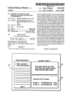
SSDA
SSDA/
9.6
AC'“
[22
XMTR 1
DIGITAL
,uP
_ CONTROL
LOGIC
26_
T/R
N
KBPS
7;
.
24 KBPS
PIA
34/
RCVR -~
361]
US. Patent Apr. 2, 1985
Sheet4 of 12
___
4,509,164
___J
m; .
v516\, 2:8
03
US. Patent Apr. 2,1985
/4
2Z5
/32
/84
-__.swITcH s \L
%
2-wIRE
DIFF.
LINE T 1/519 ' AMP
LP'F'
l- T/R
Sheet5of12
4,509,164
PEAK
/86 ,
DETECTOR
ALBO
/90
0'3"“
J
L92
TDZQEESC‘QSE’
] L96
EQUAUZER
L
FROM
TO
xMTR
_
I
/94J
I88]
BLOCK
RCVR
FIG. 5
208
§
VIOLATION
I“ DETECTOR
PIA RcvR
CONTROL
[200
‘
.
CO-ORDINAT
T/R FROM
ING
LOGIC
i__
y
>
/
XMTR
CLOCK
CLOCK
TO SSDA
REcovERY
202
206
f
F‘ M
R0
'
‘
E
UN
RCVR
—
GATING
-
2/0
I’ 5
SHIFT
REGISTER
INTERRuPT
-
PREAMBLE
i
0ETEcToR_"_’
TO CPU
J
oATA
To SSDA
2/2
ALTERNATE
INPuTs
FIG. 7
US. Patent Apr. 2, 1985
4,509,164
Sheet 8 of 12
INITlAUZE
PIA
INITIALIZE
PORTA
SSOA
“V302
V
INITIALIZE BOTH
Rx 8 Tx MEMORY
~304
BUFFER COUNTERS
if]
INITIALIZE TX‘
BY SETTING
START BIT
RECEIVER
M576‘
LATCH
V
308~
SET up ‘THE
GET Tx BUFFER
r
RESET
RECEIVER
COUNTER
'
~/3/6’
coumaas
V
r
GET THE
LOA D A BYTE
‘
RECEIVER MEMORY ~320
BUFFER COUNTER
r
SERVICE
CREATE C.W.
ROUTINE
.
324
7
WAIT FOR
IS THERE
CONTROL WORD
INTER RUPTf
INTERggPT
PRO
smeOF
BLOCK
RESTORE
MEMORY
BUFFE R
COUNTERS
FIG. 9
'NSTEQRV'TEJEPT
ROUTINE
US. Patent 'Apr.2,1985
‘
INITIALIZE PORT B
_,
OF PIA
I
Sheet90f12
332
_, 334
IIIIBSIIBSZTIIIITIII
AFTERBSSDA
4,509,164
-
I
HEX
MEMORY
“*CWHZO
I
XI
—> we = 04
x2
-—> em = 08
x3
—> CW4 = 2C
X4
CLOCK CYCLES
336
DETERMINE WHERE
THE CONTROL INTERRUPT
coMEs FROM
I
,
CW5 : IO
X5
———>' cwe = 34
X6
—> cw? = 38
x?
ALLOW FOR CONTROL
'
WORD SUBSTITUTION
IN SHIFT REGISTER
———> CW8 = Ic
\336’
I
DROP INTERRuRT REQ
RETURN
To
MAIN PROGRAM
“340
__
342
FIG. IO
X8
US. Patent Apr. 2, 1985
Sheet 10 ofl2l 4,509,164
GET THE Rx
350V BUFFER COUNTER
T
362* DECREMENT BY ONE
LOAD ACC. A
WITH CONTENTS
SPECTFIED BY
354“-
ABOVE COUNTER
i
.AND THE CONTENT OF
ACC. A WITH (IC)HEX
7
CHECK INDIVIDUAL
BlTS C2C3C4AND
358V TAKE APPROPRIATE
ACTION eg. DEFAULT
OR RETRANSMISSION
REQUEST ETC.
‘
350*‘
RETURN
TO THE
MAIN PROGRAM
- FIG. l||
U.S. Patent Apr. 2, 1985
INITIALIZE PIA
Sheet 11 of 12 4,509,164
#362
I
INITIALIZE ssDA
FOR RECEIVING
‘_364
V
I
s/w DELAY TO
__
SET'RX LATCH
366
FAKE 2 ssDA CLOCK
PULSES FOR SYNCH —--368
OF DATA AND CLOCK
I
LOAD RECEIVER
BUFFER STORAGE —370
COUNTER
‘
372
WAIT FOR
INTERRUPT
YES
K374
LOAD DATA
FROM SSDA TDR
II
NO
382 ‘
STORE DATA AT
376‘ LOCATION POINTED
BY BUFFER PT.
4""-I INTERRUPT?
ROUTINE
INCREMENT COLNTER
RESET THE RECEIVER
354‘- COUNTING MECHANISM
FIG. I2
INTERRUPT
> SERVICE
STORE THE COUNTER
US. Patent Apr. 2,1985
INITIALIZE PIA
PORT A ONLY
‘Sheet 12 0f12 4,509,164
_-385
II
INITIAuzE SSDA
——386’
V
LOAD SSDA FIFO -
wITII FIRsT 3 BYTES
390
II
INITIALIZE TRANSMISSION
BY SETTING sTART BIT
392
II
LOAD 4TH BYTE IN
SSDA FIFO
_394
Is TUF BIT
SET IN SSDA
sTATus
KEEP ON POLLING
THE SSDA STATUS
REGISTER
REGISTER?
SIMULATE
GUARD
TIME AND REPEAT
‘
"400
‘FIG. I3
1
4,509,164
_
2
plexing over a single pair of wires with a similar such
MICROPROCESSOR BASED DIGITAL TO
DIGITAL CONVERTING DATASET
set.
An additional object of the invention is the provision
of a microprocessor controlled dataset capable of gen
TECHNICAL FIELD
erating control words for communication with a re
This invention relates to data transmission sets, and
more particularly to such datasets operating as inter
motely located similar such dataset.
It is yet another object of the invention to provide a
digital-to-digital conversion data communication set
faces providing full duplex digital communication be
including a capability for generation and reception of
start and stop bits for synchronizing the receiving and
tween a data terminal and a communication network.
The network may be a public network or a private line,
in which a similar interface is provided for at least one
transmitting units and for maintaining a DC balance on
the transmission lines.
It is still a further object of the invention to provide a
other data terminal. The invention still more speci?
cally relates to microprocessor based interfaces for
transmitting and receiving data to and from the commu
data communication set in which bipolar violation sig
naling is used for transmitting control words from one
nication network in high speed, ?xed length data bursts
set to another, as well as for transmitting particular
sequences of message data.
representing communication with a data terminal at
slower rates.
Yet another object of the invention is the provision of
BACKGROUND ART
20
‘. Two wire full duplex transmission of data, as per
formed in prior art devices, typically relies on the use of
hybrids, or on frequency multiplexing.
apparatus for substitution of particular preambles to a
bipolar violation bit for sequences of consecutive zeros
or consecutive ones, in order to enable block recovery
even when consecutive zeros are transmitted and in
The use of hybrid circuits, however, is expensive and,
order to reduce the average signal energy when consec
additionally, may cause echos which must then be elimi
nated by the use of echo cancelling circuits. The use of
utive ones are transmitted.
frequency multiplexing for such transmission requires
sion of a DC balancing bit within a preamble to a viola
tion bit in order to maintain a DC balance on the line
'
Still another object of the invention is the transmis
the separation of the two directions of transmission by
the use of two different frequency bandsv Accordingly,
expensive ?lters are required. Both types of prior art
tion bits transmitted in a particular data block.
systems thus include de?ciencies with respect to trans
mission of digital signals, for example.
I
a microprocessor controlled dataset, including a trans
irrespective of the number and polarity of bipolar viola
Yet another object of the invention is the provision of
Various systems utilizing time division multiplexing
mitting portion and a receiving portion, a digital control
logic circuit, and a microprocessor for controlling the
are known.
For example, Evenchik U.S. Pat. No. 4,171,467, Eg
logic and the transmitting and receiving portions to
gimann et al US. Pat. No. 3,633,172 and Lutzet al US.
Pat. ,No. 3,974,339 all pertain to communication sys
provide ‘appropriately timed data transmission and re
ception.
tems. The Evenchik disclosure teaches the use of a
single pair of wires to interface a data and ya voice com
In accordance with these and other objects, the pres
ent invention provides a digital to digital converting '
communication interface in which a transmitter section
and a receiver section communicate with a high speed
data line through a transmit/receive controlled switch.
munication circuit using bipolar bit pair coding. The
Eggimann patent provides time compression in address
coded signaling in which discrete information packets
are time position modulated. Finally, the Lutz patent
further provides two-wire time division multiplexing in
a telecommunications network.
Digital control logic circuitry is provided for perform
ing various functions required for proper operation of
45 the device in accordance with the foregoing objects. A
None of the references, however, provide a micro
processor based communication system having the ad
microprocessor is provided, as is a ?rst serial synchro
vantages provided herein.
nous data adapter (SSDA) enabling communication
between the control logic and the microprocessor, and
In providing a functional data transmission set, it is
desirable to provide storage for the transmitted infor
mation both before its transmission and after its recep
a peripheral interface adapter (PIA) for transmitting
various signals between the microprocessor and the
control logic. A second SSDA is provided for enabling
tion. For example, information from a source terminal
communications between the microprocessor and exter
may be entering the dataset simultaneously with the
reception of information from the transmission line. The
nal data terminals.
-
BRIEF DESCRIPTION OF THE DRAWING
data to be transmitted must be stored until the dataset is 55
ready to transmit. Further, the dataset must have suf?
The foregoing and other objects, features and advan
cient intelligence to determine when to switch from the
tages of the present invention will be more readily ap
transmission to the receiving mode, and vice versa.
preciated upon reference to the following disclosure
Moreover, the desirable system should be able to gener
when taken in . conjunction with the accompanying
ate control words in order to, communicate with a sepa 60 drawing, in which:
rate similar system, and to provide error checking func
FIGS. 1a and 1b represent two environments applica
tions.
v
ble to the invention dataset interface;
None of the prior art provides these features.
FIG. 2 shows a block diagram representation of the
DISCLOSURE OF INVENTION
It is accordingly an object of the present invention to '
provide a microprocessor based dataset for communi
cating in a full duplex, burst mode time division multi
several components forming the inventive dataset;
65
FIG. 3 shows a block diagram representation of the
transmitter portion of the dataset of FIG. 2;
FIG. 4 shows the details of the block diagram of FIG.
3;
i
4,509,164
3
FIG. 5 shows a block diagram of a line receiver and
conditioner portion of the receiver block of FIG. 2;
FIG. 6 shows the details of the block diagram of FIG.
5;
.
4
THE INVENTIVE STRUCTURE
Referring now to FIG. 2, a base band modem incor
porating the present invention is generally shown at 20.
FIG. 7 shows a block diagram of a second portion of 5 The modem 20 may be used either as a slave modem18
the receiver block of FIG. 2;
FIG. 8 shows the details of the block diagram of‘FIG.
or as a master modem 16, as shown in FIGS. 1a and 1b.
The modi?cation necessary to operate the modem as a
7; and
-
master or as a slave are described in greater detail with
FIGS. 9-13 show flow charts of various programs
reference to the transmitter, shown in FIG. 4.
As is seen in FIG. 2, the inventive modem includes
and subroutines used in controlling the microprocessor
of FIG. 2.
transmitting and receiving portions, having a transmit
ter 22 and a receiver 24, connected by a transmit
receive (T/R) switch 26 to the high speed, two wire
BEST MODE FOR CARRYING OUT THE
data line 14. T/R switch 26 may be a type 4066 chip.
15 The unique features of the present modem are provided
Referring now to FIGS. 1a and 1b, a typical envirOn—
by use of a programmable micrprocessor 28, such as
ment for the inventive dataset is shown as including
model MC 6800 available from the Motorola Company,
either a private line, shown in FIG. 1a, or a public
for controlling the transmitting and receiving opera
network, shown in FIG. 1b. In FIG. 1a, a host com
tions in a manner to be described below.
'
puter 10 is shown as communicating with a user termi 20
Microprocessor 28 communicates with either the
nal 12 over, a private, two-wire line 14. A pair of base
host computer or a data terminal over a 9.6 KB/s inter
band modems 16 and 18, each embodying the inventive
face 29 through a ?rst serial synchronous data adapter
datasets, are shown connected to host computer 10 and
(SSDA) 30, such as is available from Motorola under
user terminal 12, respectively, by standard interfaces of
chip designation MC 6852, for example. In modems
25 designed for asynchronous communication with a host
the type RS232C.
or a data terminal, SSDA 30 may be replaced by an
Modern 16 is a master modem unit with timing con
'
INVENTION
trolled by host computer 10. Modem 16 transmits data
at predetermined times, and in that respect controls
response timing for the modem 18, which is represented
as a slave modem unit in the diagram. It is to be under
stood thata number of user terminals 12, not shown in
the ?gure, may be connected to modem 18 for multi
plexed communication with host computer 10.
In an alternative environment, the modems of the
present invention may be used in conjunction with a
asynchronous
communication
interface
adapter
(ACIA). The ACIA, as part of its function, adds and
removes start and stop bits for message characters at the
transmitting and receiving portions of the operating
sequence.
-
A second SSDA 32 is used to transfer data, clock
signals and other handshaking signals between micro
processor 28 and the transmitter portion 22 and the
receiver portion 24. A peripheral interface adapter
controlled by central clocks at the network offices, so
(PIA) 34, available from Motorola as chip MC 6821, for
example, communicates a number of control signals
between the microprocessor 28 and a digital control
that both the set of host computers 10a . . . 10b and the
logic circuit 36.
set of terminals 12a . . . 12b are provided with slaved
Digital control logic circuit 36 includes a number of
circuits for controlling the transmitter and the receiver,
public network 19. In this environment, system timing is
modems 1801 . . . 18171 and 18a2 . . . 18b2, respectively.
The slave units communicate with master units 1602 . .
. 16b2 and 1601 . . . 16111 over lines 14a2 . . . 14b2 and
as well as for enabling and clocking SSDA 32. Such
control of SSDA 32 permits SSDA 32 to communicate
1401 . . . 14b1. Timing and synchronization of data
with the microprocessor 28 at a ?rst, slow rate and in a
transmission on each line is controlled by the master 45 ?rst, parallel format, while communicating with the
unit associated therewith, the master unit timing being
transmitter 22 and receiver 24in a second, fast rate and
in a second, serial format.
controlled by the public network as previously de
scribed.
,
TRANSMITTER UNIT
By providing a single, centralized timing control, all
master units are caused to transmit simultaneously,
thereby avoiding near-end crosstalk. Speci?cally, inas
much as all master units transmit simultaneously, the
receiver portions of each of the masters are therefore
simultaneously disabled. Thus, any crosstalk from a
transmitting master on a ?rst line to a second line will
not affect the master modem associated with the second
' The individual components of the inventive modem
or dataset shown in FIG. 2 are shown in greater detail
in the remaining ?gures. Speci?cally, FIG. 3 shows, in
block diagram, the communication between the second
SSDA 32, the microprocessor 28, the transmitter por
tion and the appropriate digital control logic associated
therewith.
‘
_
One feature of the inventive structure is the use of
line, since the receiver portion of the second modem is
bipolar signaling. Such signaling is provided by a bipo
disabled.
lar converter 38, connected for receiving serial data
The use of microprocessor controlled datasets in 60
output from a substituting device 40 over a data line 42.
accordance with the present invention for the master
Bipolar encoded data is provided to a line driver 44, for
and slave units of FIGS. 1a and 1!) permits the desired
connection to T/R switch 26 and thereby to the two
full duplex communication over a high speed two wire
wire line 14.
line 14. Speci?cally, terminals communicating at data
In bipolar signaling a logic one consists of a positive
rates up to 9.6 kilobits per second (KB/s) may be fully 65 or negative pulse, whose width is one half the clock
duplexed over a two wire, 24 KB/s transmission line
period at the speci?ed data rate. Successive logic one
using a burst interleaved time compression technique of
bits alternate in polarity. A logic zero bit consists of a
data transmission as provided by the present invention.
zero signal on the line.
4,509,164
5
In the present apparatus, circuitry is provided for
substituting a particular sequence, or preamble of bits,
for predetermined sequences of data bits. Speci?cally, a
sequence of eight zeros is replaced by a preamble of ?ve
zero bits, a sixth bit whose value may be zero or one, a
seventh bit whose value is zero, and a one bit provided
in violation of the bipolar encoding rules described
above. That is, a one bit is transmitted whose polarity is
the same as the last previously transmitted one bit. Such
a bipolar violation is used to indicate that the seven
preceding bits form a speci?c preamble, signifying a
particular data bit sequence. As shown in the table be
low, three types of bipolar violation signaling are pro
vided herein.
TABLE I
MSB
LSB
6
control signal is transmitted by a substitution control
circuit 48 on a line 49 to the shift register 46 for accept
ing parallel input data on lines 50. The data provided on
lines 50 represents the preamble to be transmitted in lieu
of the sequence for which substitution is desired. Alter~
natively, where control signals are to be transmitted to
a receiving modem, a control signal is provided to sub
stitution circuit 48. In response, circuit 48 generates the
substitution control signal for causing shift register 46 to
accept a control preamble on lines 50.
The parallel input lines 50 provide the preamble di
rectly to the various cells of shift register 46, for output
on lines 52, including the least signi?cant bit output line
54. Output line 54 thus provides a serial data‘ output line
for shift register 46, outputting the various data bits as
the register is clocked.
The circuitry as described thus provides a serial out
put on line 54 representing either the serial input on
Control Signal
V 0
X
C4
C3
C2
C1
C9
input data line 56 or the information carried by lines 50.
20
Lines 50 are provided with data representing either the
The ?rst signal‘ sequence is transmitted, with a bipolar
zero substitution preamble, the one substitution pream
violation bit ‘V’ to indicate that the data contains a
ble, or the speci?c control signal by a multiplexer 58.
string of eight consecutive zeros. The second sequence
The input to multiplexer 58 is provided by a generator
is transmitted with a bipolar violation to indicate a
60 which generates the one and zero substitution pream
string of eight ones. The third sequence is used for
bles, and by a second set of lines, shown at 62, providing
communicating control signals to the receiver. While
control signals from PIA 34. The data output of shift
theoretically any of 32-control messages may be trans
register 46 on line 54 is also fed back to the input of
mitted by the ?ve bit preamble C0, C1, . . . , C4, the ?rst
multiplexer 58 so that the two least signi?cant bits of the
Zero Substitution
V
0 I
X
0
0
0
0
0
Ones Substitution
Y
0
X
0
0
0
l
1
two bits are provided a ?xed value, and act as a two-bit
preamble to identify a control signal. Preferably, C0: 1,
C1 =0, and any of eight control messages is indicated by
bits C2, C3 and C4. It should be understood that where
a larger number of control messages must be provided,
two bytes may be used. A ?rst byte, including a viola
zero or one substitution preambles, which are provided
to the input of the shift register by multiplexer 58 on line
56, duplicate the data represented in the string of eight
consecutive ones or zeros as provided in Table I above.
Multiplexer 58 is in turn controlled by a control signal
unit
64 which also provides controls for substitution
tion bit, may identify the second byte as a control mes 35
control
circuit 48, T/R switch 26, and a substitution
sage of up to eight bits in length.
r
inhibiting
circuit described in the sequel.
In the inventive structure, at least one one-bit is trans
In operation, ‘once substitution control circuit 48 ei
mitted upon the occurrence of a string of seven zero bits
ther detects the string of bits to be replaced,. or is trig
in the data stream, in order to permit clock recovery
gered by control signal unit 64, a signal is transmitted to
from the receive line. When at least seven logic ones are
shift'r'egister 46 to accept alternate inputs rather than
transmitted, average signal energy is reduced by trans
the serial data output of SSDA 32. Further, a violation
mission of the preamble followed by the violation bit as
generation control circuit 66 is caused by substitution
shown above. Finally, for transmission of particular
control circuit 48 to generate a violation bit by ‘appro
control messages, different preambles are provided,
priately disabling bipolar converter 38. The appropriate
characterized by various bits con?gurations of bits C2,
preamble for the violation bit is provided to shift regis
C3 and C4, as described in the sequel.
ter 46 by the output of multiplexer 58.
The “X” bit transmitted within the preamble is se
lected to be zero or one, as required, to assure that
successive bipolar violation bits alternate in polarity in
An X bit generator 68 inputs an appropriate bit to
shift register 46, in accordance with the condition of'a
counting circuit and a ?ip-?op therein responding to the
order to eliminate DC buildup on the line. Thus, if two 50
serial output stream on output line 54. A timing unit 70
successive zero substitution signals are transmitted, it is
conceivablethat, without special provision for alternat
is provided for controlling timing of the various compo
ing the X bit, three successive positive one-bits would
be transmitted. Speci?cally, the last one-bit preceding
nents of the transmitter and the digital logic control
circuitry therefor, as shown in the ?gure. In a master
the ?rst set of seven zeros, the ?rst violation bit, and the 55 unit, such as shown at 16 in FIGS. 1A and 1B, timing
unit 70 is included in or controlled by host processor 10
second violation bit. By providing the X bit in the pre
or public network 19, respectively. Such a modi?cation
amble, the second zero substitution preamble includes a
negative pulse representing the X-bit, and a second ' of the circuit permits the network or host processor to
negative pulse representing the violation bit, thereby
balancing out the DC levels on the line.
The substitution circuitry is speci?cally shown in
FIG. 3 to contain a shift register 46, receiving serial data
on line 56 from the SSDA 32. A substitution control
circuit 48 receives parallel output data from the shift
control synchronized transmission by plural master
60 units. In a slave unit, timing unit 70 is essentially inde
pendent of the network, and the unit functions in accor
dance with the timing of the received signals.
As will be appreciated, while all data transmissions
from the various masters in a network are simultaneous,
register, to detect the presence of a consecutive string 65 inerleaved responses in the duplex system from the
slave units arrive at the master units at varying times,
desirable to replace. Upon detection of a particular
depending upon the distance between the speci?c mas
sequence, such as eight ones, for example, a substitution
ter and slave units. The microprocessor control unit of
of eight zeros, ones, or other sequences which it may be
' 4,509,164
7
each master is programmed to await the reception of
data from its associated slave unit.
The furthest distance between any pair of modems on
a particular line is taken into account in a public net
work situation, so that controllers in the network of?ce
are programmed to provide a minimal guard band (time
.delay), even for the master'furthest removed from its
associated slave, prior to initiating the next universal
transmission by the master units.
8
Referring to the ?gure, it is seen that a number of
address signals are provided on lines 75 by the micro
processor to access the particular transmitter. Thus, a
pair of decoders 74 is provided for activating the second
SSDA 32 in response to the appropriate address by the
microprocessor 28. A byte of data is input on lines 76 to
the registers within the SSDA. In operation, upon a
reset signal or‘ on power up, all PIA port A lines are
provided with a high (+5 V) voltage level. The trans
In the presently preferred embodiment, ?xed length
mit receive switch 26 is reset to the receive mode on
data blocks are transmitted. Preferably, the blocks are
power up, and the third-byte substitution inhibitor 72 is
four bytes long. Since no byte separation bits are pro
vided, it will be understood that a string of eight l’s or
O’s may bridge a pair of bytes. It is also noted that the
data output on line 54 by shift register 46 represents the
least signi?cant bit of a byte of data appearing on output
lines 52. Thus, before data from line 54 is transmitted,
the seven following bits for transmission are available
on the rest of output lines '52. Substitution control 48
accordingly outputs a substitution control signal on line
49 to begin substitution before the bit stream has been
transmitted.
It is another feature of the invention that, while four
byte blocks are transmitted in a burst, the fourth byte of
a message is not transmitted until the following burst,
suppressed, or disabled, as are various counters in the
receiver. A receive mode latch is set. The receiver is
described in the sequel. All other ?ip-?ops, counters, '
switches, latches, and shift registers are considered to be
in a random state after power up.
In operation, the SSDA transmits and receives the
least signi?cant bit of each byte ?rst. Atransmit bit in a
control register C1 of SSDA 32 is reset by the initializa
tion routine executed by microprocessor 28, and the
SSD_Atransmit section is inhibited by a high input level
to CTS. The three bytes for later transmission (bytes A,
B, and C) are preloaded into a queue within the SSDA.
Finally, the ?ll) bit drops in response to a control mes
sage from the microprocessor. When the PA?) input to
remaining instead in the shift register 46. Accordingly,
AND gate 78 rises, the AND gate is enabled thus en
if an eight bit 0- or l-string begins anywhere in the next
to last byte, but not in the ?rst, or border, bit thereof,
abling the J input of a ?ip-flop 80 which generates start
and stop bits. On the next positive transition of the
' inverted clock output signal on line 83 output from
such a string must not be substituted for. If substitution
were to take place under such circumstances, the viola 30 timing unit 70, flip-?op 80 sets. A delay' is provided at
84, on the C input to flip-flop 80, in order to insure that
tion bit would not be transmitted, and the transmitted
l the positive transition of the inverted clock signal on
data would be inaccurate. That is, a one or zero pream
wire 83 arrives at C after the clock signal has dropped
ble must not be shared by separate bursts.
For example, where a four byte message ABCD is to
be transmitted, bytes ABC are transmitted during a ?rst
burst, byte D being stored for transmission as the ?rst
byte of the next burst. The next message, EFGH, is thus
transmitted as DEFG.
Examining bytes G and H as in Table II,
TABLE II
Bit Number
X
1 1000000
V
001 1001 1
12345678
12345678
G
H
at the R input of the ?ip-?op. The setting of ?ip-?op 80
sets a latch 86, and feeds a start bit to an OR gate 88.
Latch 86 is used to provide the CTS and W signals
and to control T/R switch 26.
The T/R switch 26, which preferably is a 4066 type
chip, responds to i5 v control signals. Accordingly, a
pair of transistors 87 and 89 are used in a level shifting
circuit to convert the O and + 5 v outputs of latch 86 to
+5 v and — 5 v, respectively. Thus, setting latch 86
provides the appropriate voltages for changing the T/R
switch to the transmit mode. Simultaneously, the output
45 of latch 86 enables the J input of a ?ip-?op 90, and,
through an inverter 92 and AND gate 78, disables flip
it is clear that if a zero substitution were permitted for
flop 80 thus terminating the start bit. Additionally, a
the string of zeros beginning at bit 3 of byte G, the
?ip-?op 94 in X-bit generator 68 is enable, and the C—TS
eighth bit of byte G would be replaced by an X bit
input for SSDA 32 drops, enabling the transmit section
which may be one, but the H byte, which contains the 50 of SSDA 32 for transferring the ?rst‘byte of information
V bit location at its second bit, would not be transmit
to shift register 46 as seen in FIGS. 4A and 4B, when
ted. G would thus be transmitted with an error at loca
the output of latch 86 is set, the R input to ?ip-?op 94 is
Byte
' tion 8.
Accordingly, a next-to-last byte substitution inhibitor
is provided, shown as N-l Byte Substitution Inhibit
lowered, thus enabling the ?ip-?op. The ?rst data bit
appears on output line 96 from the SSDA upon the
occurrence of a negative transition of the ?rst full posi
circuit 72, functioning to inhibit one or zero substitution
as soon as three bytes are clocked out of shift register 46
tile pulse on clock signal line 82 following release of
in a four byte burst system. For an N byte burst system,
zero and one substitution is inhibited for the (N—1)th
byte. The substitution‘ inhibitor circuit includes a
counter, and is responsive to control signal unit 64 such
that during continuous transmission, as in a test mode
82, ?ip-?op 80 is reset, thus having formed and ?nished
the start bit. In response to resetting ?ip-?op 80, the
clock input of a ?ip-?op 98 inthe substitution inhibiting
for example, inhibition is suppressed.
CTS.
On the next positive transition of the clock signal line
circuit 72 is enabled to suppress substitution inhibitions.
It is important that the P16 bit remain at a low level
Referring now to FIG. 4, a detailed circuit diagram is
for a time period suf?ciently long as to overlap the
shown for the block diagram in FIG. 3. Each of the 65 negative transition of the start bit. At this point, E0
enumerated components in FIG. 3 is shown in greater
must make a positive transition, and the last byte of the
detail in FIG. 4, including the various circuit chips and
preceeding message is transferred to a three byte trans
interconnections thereof.
mit ?rst-in-?rst-out register (FIFO) of SSDA 32. On the
4,509,164
next positive transition of the inverted clock line, ?ip
flop 90 is clocked up and the inverted Q signal thereof
transitions negatively, thus allowing shift register 46 to
begin receiving clock pulses. Similarly, the ?rst data bit
for transmission is formed by ANDing the signal on line
10
a multiplexer control signal on output line 114 from a
latch 116. This signal controls both multiplexing chips
111 and 113, the latter providing the two least signi?
cant bits of the preamble. As is seen from FIG. 4, when
control meassages are to be transmitted, the two least
signi?cant bits are provided with zero and one values
54 with the inverted clock signal of line 83 in AND gate
99, while the ?rst valid data bit appears on line 96 out
corresponding to C1 and CO. For transmission of zero
and one substitution preambles it is seen that the inputs
to the fourth, ?fth and sixth most signi?cant bits are
counter 100 is enabled to begin clocking on the next 0 zero while the inputs to the two least signi?cant bits are
positive transition of the inverted clock signal. Counter
provided as a feedback from the output data bit, so that
100 is used for driving the substitution inhibit circuit 72.
the preamble has a pair of ones or a pair of zeros to
When the signal on clock line 82 transitions posi
indicate one or zero substitution as shown in Table I.
tively, the second data bit is shifted out onto line 54, and
Accordingly, when a substitution control signal is
the least signi?cant bit of the ?rst byte of the new mes
provided on line 49, shift register 46 provides eight
put by SSDA 32.
As the inverted output 6 of ?ip-?op 90 drops, a
sage is shifted onto input data line 56 for shift register
speci?c bits for sequential transmission on output data
46.
‘ When the inverted clock signal on line 83 transitions
line 54. The register is thus seen to perform one type of
multiplexing, in which a selection is made between data
bits, provided serially by SSDA 32 on line 96 and enter
positively, counter 100 begins to count. Regular data
clocking now continues for the ?rst three bytes (A, B,
C) of the message. A secondcounter 102 is provided,
ing the register serially on line 56, or a parallel input of
the information on lines 50. The data on’lines 50 is, in
with an output for setting ?ip-flop 98 when the next to
last byte of a message is being transmitted. As is seen
from the diagram, a NOR gate 104 is disabled by the
turn, selected by multiplexing inputs either from port B
of the PIA or from ?xed preamble signals and a pair of
data replicating signals.
positive output transition of ?ip-?op 98, thus disabling
25
the substitution control signal provided on line 49.
Circuitry is provided within the violation generation
control circuit 66 for disabling further substitution dur
ing the time that the eight bits of the substituted byte
SUBSTITUTION CONTROL CIRCUIT
reside within shift register 46. With reference to the
During normal operation, however, with gate 104
circuit, the control signal output by NOR- gate 104 is
enabled, it is seen that eight consecutive output bits,
whether forming a byte or bridging two bytes, are pro
vided by shift register 46 to NAND gate 106 and NOR
also used to set a latch 120. The output of that latch,
after appropriate delay by a delay circuit 122, is re
turned to the input of NOR gate 104, thereby disabling
gate 108. The output of NAND gate 106 is connected to
any further substitution, once the signals on lines 50 are
the input of NOR gate 110 by an inverter 112. As will be
accepted by the register 46. This arrangement prevents
' appreciated, only if all eight inputs to NAND 106 are of 35 any possibility that the substitution code might itself be
the “one”, or high, level will the gate provide a high
level input to NOR 110. Similarly, only if all eight in
puts to NOR 108 'are at the “zero”, or low, level will
that gate provide a “one” or .high level input to NOR
110. Thus, in the event of a consecutive string of eight
ones or eight zeros, NOR gate 110 provides. a low input
substituted for.
BIPOLAR PULSE GENERATOR WITH
VIOLATION INJECTION _
40
to NOR gate 104, combined with a low input from
flip-?op 98' except in the next-to-last byte. If the third
input to NOR gate 104 is similarly low, the provision of
a negative low level input signal by gate 110 provides a
The data bits provided by OR_ gate 88 for transmis
sion on‘lines 14 are delayed by a delay circuit 124, buff
ered by a buffer element 126 and provided to bioplar
converter 38 including a buffer transistor 128 and a pair
45
high level, or “one” signal on line 49 which is fed back ,
of inverting transistors 130 and 132. Speci?cally, the
output signal from transistor 132 is opposite in polarity
to the output signal of transistor 128. The two bit
to shift register 46 to trigger a parallel substitution for
streams output by transistors 128 and 132 are input to a
the output data by data entering register 46 on lines 50.
multiplexer 134, having a control input generated by a
As is apparent from the connections of lines 50, the most
?ip~?0p 136 which is itself clocked by the data stream
signi?cant bit is connected to a positive ?ve volt level, 50 directly output by OR gate 88. Each l-bit output by OR
representing a “1” signal. The next most signi?cant bit
gate 88 clocks ?ip-?op 136 and thus causes multiplexer
is grounded, representing a zero input. The third most
134 to alternate the choice of input signal from transis
signi?cant bit is connected to receive the output of X bit
tor 128 or 132. Accordingly, consecutive 1 -bits are
generator 68, while the remaining 5 bits receive the
output by multiplexer 134 with opposite polarities, thus
outputs of multiplexer 58, which is comprised of a pair 55 providing the bipolar signaling desired in the present
of commonly controlled multiplexing chips 111 and
embodiment. Inasmuch as the switching of the multi
113.
it is noted that the fourth, ?fth, and sixth most signi?
cant bits receive signals through the multiplexer origi
nating either on lines PB2-PB4 of port B of PIA 34, or 60
as a ground signal. The bits from port B of the PIA
represent control bits C2-C4 shown in Table I, supra,
generated by the microprocessor in transmitting one of
eight possible control messages. The ground level, or
plexer must occur prior to the appearance of the data
bits output by transistors 128 or 132, delay circuit 124
assures that the data bits do not appear until substan
tially after the required polarity switching.
When a signal is being produced which requires a
violation bit, latch 120 is set by the output of NOR gate
104 as previously described. The latch output is used to
enable a counter 138 to begin counting on the next clock
zero bits are the three bits of the zero and one substitu 65 pulse after the one causing the substitution. In the pre
tion immediately preceeding the X bit in Table I. The
speci?c signals to be transferred to the ?ve least signi?
cant bits of the preamble are determined by the status of
ferred embodiment 8 bit bytes are transmitted. Thus, a
NAND gate 140 is used to detect a count of 7 by
counter 138. Upon detecting the count of 7, NAND
11
4,509,164
12
gate 140 provides a low-level output, used to prevent
includes no ones while the one substitution preamble
?ip-?op 136 from further changing state, thus providing
includes two ones.
a bipolar violation in the output of multiplexer 134 for
the V, or violation bit of the substitution byte. Upon
The functioning of the X-bit generator 68 is more
clearly understood with reference to the circuit dia
gram in FIG. 4. As is seen there, ?ip-?op 94, which is
\reset by the pulse output of an OR gate 142 enabling and
occurrence of the next clock pulse, counter 138 attains
a count of eight, thus resetting itself as well as latch 120
in preparation for the next substitution. This mechanism
disabling the transmission cycle of SSDA 32, is released
is operative for all substitutions, whether zero and one
substitutions controlled by gates 106 and 108 or control
at the start of a transmission block. Flip-flop 94 is con
signals similarly transmitted with a bipolar violation bit.
nected to be clocked by the data stream output by
buffer element 126. With its J and K inputs connected to
The signals output by multiplexer 134, whether in
logic one, ?ip-?op 94‘is thus clocked up by the start bit
cluding a violation or in proper bipolar code, are pro
vided to a line driver circuit 44 for input to the trans
mit/receive switch 26.
block. Accordingly, the present circuit causes the out
put of ?ip-?op 94 to be at the “one”, or high level only
THIRD BYTE SUBSTITUTION INHIBITOR
As previously described, messages are transmitted in
the present embodiment in blocks of four bytes, the last
and by each subsequent one-bit during that transmission
15 for previous transmission of an even number of one bits
in a particular transmission block. It is precisely under
such circumstances that the X-bit of the preamble must
itself be a one. The output of ?ip-?op 94 is accordingly
byte of a particular block being held over in register 46
input to the third most signi?cant bit of shift register 46
for transmission as the ?rst byte of the next succeeding 20 on lines 50 to provide the X-bit of a preamble transmit
block. This approach results from a serial transmission
of data from SSDA 32 to shift register 46.
Speci?cally, when a data byte is serially transmitted
from SSDA 32 to the shift register, the byte then resid
ted thereby.
.
For transmission of control signal preambles, how
ever, there 'is no guarantee that the number of one-bits
in the ?ve least signi?cant bits of the preamble is indeed
ing within the register is shifted out of register 46 for 25 even, as required to maintain the validity of the X-bit.
transmission. That is, the Kth byte of a ?xed length
Particularly, as previously described with respect to
block output by SSDA 32 causes transmission of the
Table I, the C0 and C1 bits are predetermined to be one
K-lst byte from register 46. Thus, after transmission of
and zero, respectively. The C2, C3 and C4 bits, repre
four bytes of a particular block by SSDA 32, three of
senting any of eight possible control messages, must
the bytes have been transmitted by register 46 through 30 thus have an odd number of l-bits in order to retain the
line driver_44, and the fourth remains within the register
validity of the X-bit. If all eight possible control mes
for transmission as the ?rst byte of the succeeding
sages are to be transmitted, however, it is seen that only
block. Accordingly, as soon as the last byte of a block
four permutations of the bits C2, C3 and C4 have an odd
begins to be transmitted from SSDA 32 to register 46,
number of l-bits. For control messages in which either
one or zero substitution must be disabled since the gat 35 none or two of the control bits C2, C3 and C4 are ones,
ing circuitry comprised of NAND gate 106 and NOR
gate 108,, detects any eight consecutive ones or zeros,
including a consecutive string bridging the last two
bytes of a block transmitted by SSDA 32. Since the next
the X-bit itself must be inverted prior to being provided
to the input of shift register 46.
Towards that end, an exclusive OR circuit is pro
vided at 144. The inputs of the exclusive OR circuits are
to last byte of a block output by SSDA 32 is, in reality, 40 provided by the output of flip-flop 94, on the one hand,
the last byte of the block to be output by register 46, any
and the output of an AND gate 146, on the other. AND
such string of consecutive ones or zeros overlaps two
gate 146 receives as its inputs a control signal PBS, from
separately transmitted data blocks. Such an overlap
port B of the PIA 34, and the multiplex control signal
leads to an error in transmission as shown above. Ac
provided on line 114. The signal on PBS is provided by
cordingly, counters 100 and 102 and ?ip-?op 98 form 45 microprocessor 28 in accordance with a determination
the substitution inhibiting circuit 72 for disabling substi
of the values of control bits C2, C3 and C4. In the pre
tution after 24 bits have been plucked out of register 46.
ferred embodiment, in which the multiplexer control
signal on line 114 is at a high level, multiplexer 58 trans
X-BIT GENERATOR ‘
mits the control bits provided by lines PB2, PB3 and
In order to provide complete DC cancellation of the 50. PB4 from port B of PIA 34 to the shift register. Under
effects of transmission of positive or negative one bits,
those circumstances, a software operation is used by
from the start bit through to the violation bit, an X-bit is
microprocessor 28 to determine whether the number of
generated in the violation preamble. As previously de
l-bits on lines PB2, PB3 and PB4 is odd. If the number '
scribed, the X-bit will be either a zero or a one, appro
is odd, PBS is left at a low level. If the number is even,
priately selected to maintain DC balance on lines.
The X-bit itself is determined at the time a substitu
however, the signal at PBS is provided with a high
tion, or control signal is required. The determination
occurs prior to the transmission of the least signi?cant
bit at Table I, supra. More speci?cally, the value of the
X-bit is determined prior to transmission of the ?rst ?ve
number of l-bits in the 5 bit preamble C0, C1, C2, C3,
bits of the preamble. Since an even number of ones
includes as many positive bits as negative bits, no DC
buildup is effected thereby. Accordingly, the number of
level. The PBS line is thus at a high level when the total
C4, is odd. ‘
The output of AND gate 146 is thus provided with a
high level only under conditions where a control signal
is to be transmitted to the shift register and the control
signal violates the requirement for an even number of
one bits in the ?ve bits preceeding the X-bit. As is
one-bits in the ?rst ?ve bits of the preamble must be
known in the art, a one input on one of two lines enter
even, in order not to disturb the DC cancellation pro 65 ing an exclusive OR leads to an output which is the
vided by the already determined X-bit. Forthis reason,
complement of the second entering line. Thus, under
both preambles for zero and one substitution include an
even number of ones. Speci?cally, the zero substitution
the above-identi?ed circumstances in which AND gate
146 provides a one output, the signal provided to shift
4,509,164
13
register 46 is the complement of the output of flip-flop
14
sion onto lines 14 and for balancing the DC level
thereon. After a delay by delay circuit 124, the stop bit
94. Under any other circumstance, the output of AND
gate.146 is a zero level, and accordingly the output of
clocks flip-flop 94, raising its 6 output to NAND gate
exclusive OR circuit 144 the same as that of flip-flop 94.
154. The Q output of ?ip-?op 80 passes through NAND
For transmission of either a bit string substitution, or for
transmission of control signals having an even number
gate 154 to reset ?ip-?op 152 as well as latch 86, thus
?nally terminating the block and switching latch 86 to
the receive mode.
the output of flip-?op 94 is provided by the circuitry of
If ?ip-?op 94 is in its reset state, however, no balance
FIG. 4 as the correct X-bit for the preamble. For situa
bit is required. In this situation, it is seen that all inputs
tions where a control signal includes an odd number of 0 to NAND gate 154 are high, thus resetting ?ip-?op 152
l-bits in the preamble, an inverted form of the output of
and latch 86, thus switching to the receive mode with
?ip-?op 94 provides the correct X-bit. The X-bit gener
out generation of the additional balancing bit.
ator 68 thus assures the desired DC cancellation.
It should be understood that the end of a transmission
Upon each occurrence of a violation bit, as indicated
block may be detected by software. Speci?cally, a TUF
by the occurrence of a “one” level or high pulse signal
signal, indicating that the three byte FIFO is empty, is
of l-bits in the least signi?cant ?ve bits of the preamble,
at the output of NAND gate 140, the X-bit ?ip-?op 94
generated by SSDA 32. In a private line, microproces
is set to one, indicating an even ‘number of previous
sor 28 may poll the associated SSDA to determine the
completion of the various transmissions. In a network
environment, a central computer in the network of?ce
l-bits in the block, thereby to start counting anew with
the occurrence of further l-bits in the remainder of the
transmission block.
‘
20 may poll the various SSDA units for the same purpose.
The present X-bit generator‘ thus provides a DC can
cellation bit assuring that an even number of bits are
transmitted right up through the transmission of a viola
tion bit. Moreover, the X-bit generator assures that
violation bits transmitted in the same block have oppo
The above described circuit, however, eliminates the
need for polling the status registers of the several SSDA
units, and avoids an attempt to disable the SSDA by
depending on a signal which was internally generated
by itself.
site polarities.
CONTROL SIGNAL GENERATION
A control pulse is provided in order to generate an
STOP BIT GENERATOR-END OF BLOCK DC
BALANCE
Upon termination of a tranmission of a block, a signal
is required to be generated and transmitted to micro
interrupt signal to enable loading of the control bits C2,
C3 and C4 into shift register 46. The control pulse is
provided by PIA 34 on its A port, on line A1, although
it is equally possible to provide such a signal on other
lines thereof.
processor 28, as well as to switch the SSDA 32 to a
receive mode. In the present embodiment, a counter 148
is provided to supply a signal indicative of the end of a
The control pulse is generated by microprocessor 28
transmission block. The counter- 148 is reset by the 35 using a software routine, and provided to a set terminal
signal provided for resetting counter 102, and is enabled
for a ?ip-?op 158. Flip-flop 158 which acts as a latch for
by the output' of that counter 102. In essence, counter
storing the control pulse, is left undisturbed until the
148 overrides clocking of the register 46 once the fourth
control word has been loaded into the shift register. At
byte of the transmission block is established therein.
the beginning of the shiftout sequence for shift register
Counter 148 is used to reset the transmitting section as 40 46, ?ip-?op 158 is reset by the output of a flip-?op 160.
well as to generate a stop bit to provide DC cancellation
The same signal is also used, after a delay, to disable
at the end of a block.
SSDA 32.
Counter 148, which is enabled by the output of
Flip-flop 160 is connected to be clocked by the output
counter 102 and clocked by the clock signal on line 82
of a counter 162, in turn clocked by the internal clock
by timing unit 70, is used to provide an output signal on
line, and to be reset by the output of a further counter
line 150 as soon as four full bytes have been processed.
164. Flip-?op 160 is used to time the period of the shift
Speci?cally, the output signal is generated upon deter;
register in order to permit the bits stored therein to be
mining that the fourth byte output by SSDA 32 is estab
lished in register 46. The output signal of counter 148 is
used to clock a ?ip-?op 152, in turn resetting ?ip-?op
90, thereby to stop supplying a clock signal to shift
register 46 and to disable the register from accepting
further data from SSDA 32 or from further data shifting
to the transmission lines.
At this time, ?ip-?op 94 is used to determine whether
a DC balance bit must be generated at the end of the
transmitted block in order to provide an average DC
voltage level of zero for the block.
If the ?ip-?op 94 is set, its 6 output signal is low,
transmitted. The timing of this period is achieved by
using the output of counter 162 to clock ?ip-flop 160.
50
Counter 162 speci?cally provides timing for disabling
SSDA 32. This counter is reset by the output ,of counter
100, which generates a pulse every eight data bits.
Counter 164 is used in conjunction with ?ip-?op 160 to
provide the duration for the SSDA disabling pulse. A 7.5 bit duration is required for the speci?c circuit com
ponents utilized in the presently preferred embodiment.
Counter 164 is clocked by the output of an OR gate 168,
having as one input a component of the a? signal and
- as the other input the inverted .clock signal. To assure
indicating the requirement for an additional balance bit. 60 that the shift register fetches the last output bit f2
A NAND gate 154 is disabled by this low signal. How
SSDA 32 prior to disabling of the SSDA by the CTS
ever, flip-?op 152, which was set by the output of
signal, a delay circuit 166 delays the application of the
counter 148, in turn sets ?ip-?op 80 through an OR- gate
disabling pulse to SSDA 32.
156. Flip-?op 80, which is the start and stop bit genera
A pair of flip-?ops 170 and 172 provide a control
tor, thus generates an additional bit upon occurrence of 65 signal on a line 174 to shift register 46 to enable loading
the next clock pulse, at the end of the transmission
of the control word. The loading pulse is provided if
block. The additional bit, the “stop bit”, is passed
through OR gate 88 after the 32nd data bit for transmis
and only if the shift register’s data has been emptied out.
As is seen in the circuit diagram, the disabling pulse for