1
NATIONAL RADIO ASTRONOMY OBSERVATORY
CHARLOTTESVILLE, VIRGINIA
ELECTRONICS DIVISION INTERNAL REPORT No. 271
225 GHz ATMOSPHERIC RECEIVER - USER'S MANUAL
ZHONG-YI Liu
AUGUST 1987
NUMBER OF COPIES: 150
225 GHZ ATMOSPHERIC RECEIVER - USER'S MANUAL
Zhong-yi Liu
TABLE OF CONTENTS
. 1
. .
.
Introduction ...
General Description ................ ........... ............. 1
. 3
Local Oscillator ...........................• • • .... • .
.
3.1 Temperature Coefficient of the Gunn Oscillator • •
3
. 3
3.2 Tripler ..
5
Quasi-Optical System ......................... • .... • • •
4.
4.1 Chopper Wheel ......................... ............ . . 5
4.2 Lens and Injection Cavity ............................. . 10
Mixer and IF Amplifiers
5.
Synchronous Controller, Chopper Wheel Driver, and
6.
0
Synchronous Detector .................... ..............
.........' . 112
6.1 Chopper Wheel Driver ................................. 12
6.2 The Synchronous Controller ......................... . . 12
6.3 Synchronous Detector ......... .... ............. .
- 16
. 18
Elevation Mirror Driver ........................... . .
7.
7.1 Mirror Scanning Direction Control .................. . . 18
. 20
. .
7.2 Go Zenith Control .
. . 20
Interface and Data Link ........... ........... .
8.
Calibration and Result .................................. ... 20
9.
10. Acknowledgements ........................................ . 22
. 22
. .
11. References .
1.
2.
3.
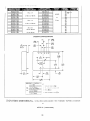
TABLES
Table 1. Tripler Bias and Perforamnce Data .
Table 2. Mixer and Receiver Parameters . .
FIGURES
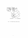
Fig. 1. Block Diagram of the 225 GHz Receiver ..................
Fig. 2. Comparison of the Temperature Coefficients Between
.
the Original and the Improved Gunn Oscillators
Fig. 3. Relationship of the Tripler Output Power and Bias
Voltage and Pump Power . . . ..
Fig. 4. The Photograph of the Quasi-Optical System ..............
Fig. 5. Outward Appearance of the Quasi-Optical System ...........
Fig. 6. The Projection of the Chopper Wheel in the Focal Plane
Fig. 7. The Mount Angle of the Chopper Blade ....................
2
4
4
6
6
7
7
Fig. 8. The Chopper Blade and Mount Block ......................
Fig. 9. Injection Cavity's Frequency Features with Different
Backshort Settings .................................
Fig. 10. Chopper Wheel Driver .................................
Fig. 11. Synchronous Controller ...............................
Fig. 12. Waveforms of Signals .................................
Fig. 13. The Motion of the Blade Switches the Beam from the Sky
to the Reference Load and the Square-Law Detector
Output Waveform ...................................
Fig. 14. The Angle of the Beam Cut-Section Opened to the Chopper
Wheel Shaft ......................................
Fig. 15. Synchronous Detector .................................
Fig. 16. Elevation Mirror Driver ...............................
Fig. 17. The Calibration Result ...............................
9
11
13
13
14
15
15
17
19
21
APPENDICES
Appendix
Appendix
Appendix
Appendix
Appendix
I
Photograph and Schematic of Square-Law Detector
23
Temperature Controller ........................... 24
II
III 12V Power Supply and DC/DC Converter .............. 26
IV
Connector Wirings ............................. ... 31
V
Layout and Wiring of Wire-Wrap Card .............. 37
225 GHZ ATMOSPHERIC RECEIVER - USER'S MANUAL
Zhong-yi Liu
.
INTRODUCTION
The 225 GHz atmospheric receiver is controlled by a desktop computer.
The system will automatically start when the 12V DC power supply is turned
on All of the sixteen analog monitor points (three of them are spare)
are scanned, scaled, and the values are displayed on the CRT screen. The
control commands and some special key functions are also shown at the
bottom of the CRT screen [1]. Operation of the receiver does not require
reading of this manual. The manual is mainly written for those who are
engaged in construction or maintenance of the receiver system.
In most cases, it is far more difficult to maintain a machine than to
operate it This is because there are concepts which are self-evident to
the builders and designers but may not be so to other persons. Some
important and useful information can only be obtained by experiencing the
process of designing, constructing and testing. So, a written description
may help to explain some critical points or give some information or clues
which are obscure in the schematics. With such an intention, this manual
will not cover every subject but will emphasize the important points.
However, an overall view of the system will be presented.
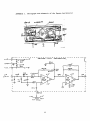
2.
GENERAL DESCRIPTION
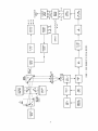
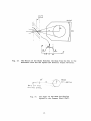
A block diagram of the 225 GHz atmospheric receiver system is shown
in Figure 1. The rotatable mirror M1 is a section of a parabola with a
focal length F — 1.2" and a beam width of 4 degrees. This beam can be
scanned from zenith to horizon with a step angle of 1.8 degrees under the
control of computer. The beam is chopped at the paraboloid focus by
chopper wheel C which switches the beam from the sky signal Ts, to referenceload signal Tr, and to hot-load signal Th sequentially. The chopped beam
is then reflected by a fixed mirror M2, passes lens L and finally enters
the feed horn H.
The local oscillator signal is generated by a commercial 75 GHz Gunn
oscillator G and is then frequency tripled to 225 GHz by the NRAO-made
tripler T. In the injection cavity I, the LO power is split into two
halves. One-half of the LO power is combined with the signal received by
the feed horn and injected into the mixer M, the other half is a spurious
signal emitted into the sky by the feed horn. The 1.5 GHz IF signal is
amplified by amplifiers AMP1 and AMP2 and is filtered by a bandpass filter
F. The chopped 1.5 GHz IF signal drives the square-law detector and DC
amplifier with output proportional to the power (or temperature) of the
total signal entering the mixer.
The output of the square-law detector is synchronously detected by the
synchronous detectors to give outputs proportional to (Ts - Tr), (Th - Tr)
and (Tr + Tsys), where Tsys is the system effective noise temperature. The
output (Th - Tr) is used for absolute gain calibration of the system. The
ELEVATION
MOTOR
GUNN OSC.
REGULATOR
GUNN
OSC.
ROTATING
CHOPPER C
BLADES
Ts
SKY
BEAM
L
'Ior
BIAS
SUPPLY
TRIPLER
J
REFERENCE
LOAD 45°C
SHAFT TO
BLADES
n
FEED
IF
AMP 1
CHOPPER
MOTOR
1--2 GHz
FILTER
CHOP.MOTOR
DRIVER
DC POWER
12 V
FIGURE 1. BLOCK DIAGRAM OF THE 225 GHz RECEIVER.
MIXER
CAVITY '
T
/ HORN
INJ.
\
)k---11-4."4C
_
LENS
FIXED
MIRROR
COMPUTER
REFERENCE
GENERAT.
CONVERTER
DC/DC
IF
AMP 2
RS232
SYNC. DET.
TO SYNC.
7;
- al
GZ
MONITOR
CONTROL
CW
CCW
Ts—Tr
SQ.—LAW
DET./DC AMP.
SYNCH.
DETECTOR
TH—Tr Tr
SIP
ELEVATION
MOTOR
DRIVER
TO ELEVATION
MOTOR
temperatures of Th and Tr are exactly controlled at 65°C and 45°C,
respectively, by the temperature controllers.
The monitor and control board links the receiver with the computer.
The computer controls the elevation angle and monitors the receiver's
working status and measurement results. A reference generator at a frequency
of 4 KHz, after frequency dividing, drives the chopper's motor driver (IC
SAA 1027) and the synchronous detector and the elevation motor driver (IC
SAA 1027) is driven by the computer's control signals.
3.
LOCAL OSCILLATOR
Local oscillator power is generated by a commercial 75 GHz Gunn
oscillator (Millitech Model GDM-12T). Some important parameters of the
Gunn oscillator which have been carefully examined before being used in
the receiver are the frequency stability, output power, and the effects of
load impedance.
3.1 TEMPERATURE COEFFICIENT OF THE GUNN OSCILLATOR
In order to insure that the receiver will work in summer and in
winter, the Gunn oscillator must have a good stability with respect to the
variation of its physical temperature. The component plate of the receiver
is temperature controlled by a proportionally-controlled heater, but there
may be as much as 15°C variation inside the receiver box for a -20°C to
+50°C outside temperature variation. Because of the narrow bandwidth,
about 0.3 GHZ, of the injection cavity, the frequency shift of the Gunn
oscillator must be less than 0.1 GHz, i.e., the temperature coefficient of
the Gunn oscillator must be less than 7 * 10-6/°C.
The initial Millitech Gunn oscillators exhibited large temperature
coefficients and step changes in frequency as shown in Figure 2. Those
were returned to Millitech and much improved units were received. The
improved Gunn oscillators have a temperature coefficient of about
-5 * 10 -6 /°C and no frequency step changes were observed.
The original Gunn oscillators also have large step changes in frequency
(about 0.5 GHZ) when the load impedance was varied but this also was
corrected in the new units.
The output power of the Gunn oscillator should be more than 40 mW in
order to provide a sufficient pump power to the tripler.
3.2 TRIPLER
The tripler is designed at NRAO. The theory and constriction
were described in papers [2] and [3].
The adjustment of the tripler must be performed carefully in
order to achieve the best conversion efficiency. Because of the highly
nonlinear capacitance versus bias voltage law of the Schottky diode,
adjustment of the DC bias voltage is necessary (while tuning the backshorts)
to find the best bias point. Figure 3 gives the relationship of the
tripler output power to its bias voltage and pumping power. For each bias
3
r
TT r
.
r
r
ir 1
i
,1
,4- r
, IL
.
.L4
i
_:1
t-
1111
I 11111161 '
AI
;J
1: 4
.-4
I
'.. ...
4
u., 1
..
_
11:
1!..i
r
L -
.
*au 011.IWI
I ill
o p,.,
L4
1
,,
ill.
l
i
lGili gl
Iit
..
ii Ill '
'
I
-,
1
. fi i
7.
' 41 7I
I
T
i
i I1I
! '}
I'1
Il k
1
1 ,
, ,
L
74 0
I
1
I
/,
i
'
1.1_1
1
I I rt
I
1
1
1
i
Ir
1
ii
I
1
1
+4 i-
'
f - rrt
41t
i i.
;
I
1
-
"-- - r
tri t 17 1
1,1
'IAli
- **
i
7.
I
--i .
'
1)"
_t 1 .4 , .1-
,
" 1-
I
I, • I
1
111I
I
I
1
i
--1 !
rii,
'
t,
I
ii
,1
.. I'll
.
I I
__L.
1
i i.1' •
1_.• ., i d .:.._ '
.
1
1
t
1
, •
I
,
,
.
.,.4
Iti
! I
';
II I
1
1:
I
4
lir
1
°T i ll
7
I +.
rt- T Hip
• •
t- .
10
1 I1
-
i
4
h
I 1!
li
i. ti.i . i.
.
Fig. 2. Comparison of the
Temperature Coefficients Between
the Original and the Improved Gunn Oscillators.
--_,..-_-- - .
-- --i---=
--.:--'
- - -----:-..---..---_-=-..--_-= --: • -----:.::-..:-...--4.
- ------::-_-.----------:=----......-.---..---=.::=.7.1.1-........... ...
-.
._1_
-:-7--:-77
-8-7
_
-.-- -........•
..1 • 4 .711C1r....; - -....._.
____
_..,......_
_____._____
._ ____ _. __ . ___ . _ -..--• .---.......- - ----= --===-.......•
...5., .3
m
_22--""-:=::-7 :"--- - _:::_ii:EF-1-7.:-:.--:-.:- _i_ ' LTEIF- - ,:.::--..:::-.7-2:-._"-:: '.i.iii-E-:1-:•=
-414....0:12*"4:3Eg.
_,--- - ..:-_-::--:_-:-.
r---:
"
:
:--_____ __ ___ _
11:
1
. . " . . " . ''''- • :7 ". i i .:D ti , i
- -.
-=
- --- - - ____=.---=-
----.7.----.
----
-
-----.7.,
gaffilatElt,A1=.."-..'..".‘-'...."..----
-_-r---t-..
.
• c.
r -,r.--,. -:.,..-: 'L..
- --=-- ,-, --, - - - -- "iidialg
- - ,----,--,
.... - :. ._ ":"-- _-_:
...++.
• :::::=""•"" =-.=- - —
.7-------.
..,
iginghMik
a..
'`•
..--,...........
._—__.----------::::—
-151A;:-'----"--- .-Nk„
- ,,,EMI
. --=- _.....- -----1-_--:-.--_
. --?.....:
- : ===---,---„TaggiAtilgth,
--=:7---#-::--:-:-:7-----"=”___
'"E‘s
Nk.
::—. 4?-4
--77.7"."="
a t r■ -_-..._ =.. --:_-,e : .-....
- - • - —7710,......e===r---z r iiii
---......-- --,
'---1
.....
..
.....
.44........
"'"'
.c
....
. .!A . l'
_.
-
'
,. . . . ,. - ,....-...... ,
--
=ite."
--
-
iTigairt....====,....
......... 4, ..,,'..-....111
-4/
—=7—...-......--..—•
___:__:_-°...:
----___
.
-..
..._
4:::, Vih&.—.
"C.,==....4
-1-,ia
.
:-.7=
. . . . 4.,..5__
ih,,,...........,............,..,„...,..,■„...„,,.„.„..
_,,.. ..
.. ........%
.;IiL
_,......,..-11
S.
_ - ,,„
__-......
,
liE etil4,. .
--7.7--se====.1...
__
-.. ,
...._,
-,
...........
__-_e DltKQ5z---------.-----'-:-------_ ...-.
.
.
^
.--,.
-1:
:6,.,
_
•===ii...-.............--___- - --- -_-= - - -'.1===m7.6....-..............- ---- . 7:77,
- ---------=-..
--=E-=:.„-=;.
. _= -7-.:-._.- ___=.:.-_-.7=7.=.-_ ____
...- - •-•
_.--.= -_-_--._-.___.= 7_=:: _ _-T-..----,
.
- - -...- -
_
--4 1
-.
-..--.
-----•
----7,--=-----......-.. - --• - - - ----
4
li t
a S)
" ' .---- ' - "-.-=... -=.:--"'"
..-...-.....="'""
-' ---- ...........-..............-....
Fig. 3. Relationship of the Tripler Output
and Bias Voltage and Pump Power.
4
Power
voltage and pumping power the backshorts are tuned. As shown in Figure 3,
when the DC bias and the tuning backshorts are optimized, the peak conversion
efficiency is 5.3 percent.
Table 1 gives the four triplers' optimum bias voltages, output
powers, and the Gunn oscillator pump powers.
TABLE 1. Tripler Bias and Performance Data
Tripler
Number
.
Used in
Receiver
Optimum
Voltage
Pump
Power
Output
Power
A
4
B
2
567V
52.1 mW
1.87 mW
C
3
5.50 V
51.0 mW
2.20 mW
D
1
556V
48.5 mW
2.30 mW
QUASI-OPTICAL SYSTEM
The quasi-optical system consists of the elevation mirror Ml, fixed
mirror M2, chopper wheel C, and lens L. As mentioned previously the
chopper wheel plays a very important role in the system. It switches the
incident beam sequentially from0 the sky signal to the reference load
(45°C), and to the hot load (65 C) under the control of the chopper motor
driver and the reference generator.
4.1
CHOPPER WHEEL
The chopper wheel consists of four blades which are mounted on
the surfaces of a cubic block (see Figure 8). It rotates around its axis
as driven by the stepper motor. When the chopper blades pass through the
beam, they block off the path of sky signal coming from elevation mirror
and reflect the thermal emission of the reference load (mounted over the
chopper wheel) or the hot load emission (mounted beneath the chopper
wheel) on alternate blades. Between two adjacent blades is a window for
transmission of sky signal. The width of the window should be equal to
the width of the blade's projection in the focal plane in order to have
equal time periods for the three paths (sky, reference load and hot load).
Figure 4 is a photograph of the quasi-optical system and Figure
5 is its outline drawing. Figure 6 shows the projection of the chopper
wheel in the focal plane. The distance R, shown in Figure 6, from the
focus of the mirror to the axis of the copper wheel, is 1.61 inches. So,
the projection width of the copper blades can be calculated as
5
Fig. 4. The Photograph of the Quasi-Optical System.
Reference Load
Chopper
Wheel
Mirror
(
Lens
Injection
Cavity
Fig. 5. Outward Appearance of the Quasi-Optical System.
6
ABSORBER
EFFECTIVE
REFLECTION
AREA
ABSORBER
Fig. 6. The Projection of the Chopper Wheel in the Focal Plane.
3 "
3
,/
ti? /25'1
FC CUS
ti4
RRCR
FCCAL
pLANE
Fig. 7. The Mount Angle of the Chopper Blade.
7
B = 2 * R * Sin 22.5° = 1.232"
The angle between the axis of the beam and the normal-line N of the blades
is not 45 degrees' but an angle A which directs the beam to the center of
the absorber when the blade is at the focal position (see Figure 7). The
distance from the focal point to the absorber is 2.125 inches, and is 1.30
inches from the center of the absorber to the focal plane. The angle A is
then given by
A = 0.5 * [90° - tg - (1.30/2.125)] = 29.27°
We can now calculate the blade's width W as
W B/Cos A — 1.412"
The area of the effective reflection area on the fixed mirror
surface equals the projection area of the lens on the mirror. The radius
of the lens is one inch and the focal length F is 2.562 inches. When the
blade passes the beam, the width of the cut section will be
d — 2 * (R/F * 1/2 W * Sin 29.27°) — 0.269"
Now the height of the blade can be determined as
h
R + d/2 -a/2 — 1.35"
(see Fig.6 and Fig.8)
An optical-interruption wheel (OIW) is located on the same shaft
as the chopper wheel. There is a narrow slot in the edge of the OIW,
through which an infrared emitting diode is coupled to a photo-transistor.
When the shaft turns, the photo-transistor will send out a pulse each
turn. This pulse is used to synchronize the chopper driver and the
synchronous detector. The relative position between the chopper wheel and
the OIW is carefully adjusted. Unless necessary, do not readjust. Any
'If the absorber was a perfect load, it would be possible to make the
angle of the blades 45 degrees. The spurious LO signal emitted from the
feed horn would reflect off the blades, arrive at the absorber and be
absorbed entirely. The absorber is not perfect, though. A somewhat
attenuated signal, which is still strong enough to affect the bias point
of the mixer, is reflected off the absorber. With a 45 degree blade
angle, this returned signal travels back to the feed horn and from there
to the mixer. Choosing some other angle causes the reflected signal to
miss the feed horn entirely.
8
Fig. 8. The Chopper Blade and Mount Block:.
9
movement of the relative position will cause a synchronous error and
reduce the measurement precision.
4.2 LENS AND INJECTION CAVITY
The teflon lens is
inches. Its focal length is
is planar and the other side
formulas [4], [5]. The lens
to reduce reflection losses.
circularly symmetric and has a diameter of 2
1.2 inches. The surface toward the feed horn
is curved as determined by a set of parametric
surfaces are concentrically grooved in Order
The RF signal received by the feed horn is fed to the injection
cavity where the RF and the LO signals are combined together. The cavity
is a resonant device. It performs as a bandpass filter for the LO signal.
The central frequency and the bandwidth are closely dependent upon the
tuning of the backshorts (see Figure 9). The criteria for optimum tuning
are as low an insertion loss as possible at the LO frequency and as high a
rejection as possible at the sidebands. Since a frequency sweeper that
works in the range of 220 GHz to 230 GHz was not available, the process of
tuning the injection cavity was laborious.
Figure 9 was obtained by using a klystron and a frequency tripler
as the signal source. The klystron drove the tripler via a variable
attenuator and the tripler drove the cavity. The klystron output frequency
was tuned from 74.5 GHz to 75.5 GHz with steps of 0.1 GHz. The tripler
was retuned and the attenuator was adjusted to maintain a constant output
power to the cavity in the frequency range from 223.5 GHz to 226.5 GHz.
The listed input and output powers of the injection cavity in Figure 9
were measured at 225 GHz with the different backshort settings.
5.
MIXER AND IF AMPLIFIERS
The mixer is a single-end device [6], [7]. RF and LO signals are fed
into one port of the mixer. A GaAs Schottky-barrier diode chip is mounted
in the reduced height waveguide and is contacted with a gold whisker. The
mixer tuning is achieved by employing a fixed backshort which is implemented
as a section of short circuited waveguide electroformed into a backing
plate. There are various backshort plates with a range of diode-to-short
spacings available for optimization. In order to achieve the desired
performance, the LO power and the DC bi4s levels should be carefully
adjusted when trying backshort plates. With each adjustment we can find
the changes of the system noise temperature directly from the CRT monitor
display. The system noise temperature of the receiver #1 is less than
1500 K with mixer #23. The LO power, measured at the output port of the
injection cavity, is 0.85 mW. DC bias is -0.8 volts. Diode current is
1.45 mA. The mixer bias data, as well as the resulting system noise
temperatures of the four receivers, are listed in Table 2.
The mixer IF output is fed to the preamplifier which has an 1 to 2 GHz
bandwidth, 38 dB of gain, and 1.1 dB noise figure (Miteq Model AFD3-01002013). The amplified IF signal, through a filter and a 20 dB attenuator, is
fed to the post-amplifier which has a gain of 40 dB .
The square-law detector has a square error of 0.2 % at an IF bandwidth
of 1 GHz [8].
10
..
-
.... ,
..
.
.. . .
•
. . . ..
•. 1,..
-F..,77,, 7
--
- - -
.-- ..
ritak
:..:::-.:.....: :..":-.E...::-...: . ,.... -- : .: .
.
... _,__ *......
.. _ _ _ A
._
1-::
•-'-'.:::_i,:i
.-.:"-_
. .::::::::::--_-_::-.7.----::-..1_
._ ........-.......--.
---
.-
, -. :7..
,
-
- - .._
7,.7 7.7 - .7
-
:
. --.. .-------•
-T. , . :7-,-,
. ..-... ....... . ..._ .....--- - • .... ..1
-
=.
"--
-
. _ . .... _________
- _ .
_-_-_-:._=_---_-.:-. .
- . ._:-- ___-_....:—..:.....
... _ ....._-_---::-.
,..--.:. • --_-_-_-_. ---
:-.....-7-".".--t- i:.-:-
.
.. 7.'..7.'7.: '
:,,,, . . . • , . . - .. . . ........ ..............-.
--- --:
--..'' ' ..
' ...-
- :: :-:.--
-- • :-........,-.T.7:.7 : - -7 -
Mr
.
_ ___._____ .
.-4 -
-
--.
-.---4
.=
.
-
.
,:-.=
.IMILIk
.._.■.....-....,.. _ .
:-. . .7. ,-............-:.-=',....=.-.......=!.
/j
-- ... _
.
-
,
..... __._____•__.
_
.
:77.-- . -7.-,-,,... ...._..... .
....- .F:.,:-..----:-.--- ,. ,:-:;.:;:•:_•-_-..:,•_...-..E...-: . _
--,.-:_:-.-i-_-:.•.::---._ H:-..:
-.....,:-...,
•-. ..
-_-__----.._....-_ -_-_-_-7--:
. ______
_._-_-_-.:._
_ -•
_
....
---=------- -:-.
_
- --
,• • • • •
------,,
-
__. .____
- *---i-
-. . .
i.
' • ..: .. ..:_: J.T.: ...
- -------L1
- .1 . -- -- --:--'
_ . -- *-- • _.-- -- :--- - .-----i.,--7_ _---i-7.
_:
----:-E
..
.._ .
_ .._. _ _ .
-,epu
4CKSMOir
:-."..... .-• . . . : ...- eur
-Peva
t,,,, ) • - .
cbt-rmwea
. i . _ . . .... ,. _ _
...424 . i•-:
.„, 7„
:..... .......1.-,.-_.-,e,
..
.
_ .._-_,
. ..
o'
• 7 --.'-•.:il"..C.-r!./.1?e,4t.t . C 2 .es.)",Nr:
..
- _..- .. ,;-_---_,_-_-:-__-_-..-. _-:_.--_._
i -x--1.(--,g7.: ::..R7-2.-;Croug : . : . .1.•$* ,,,,,.., . , -. ...2 ....':--::.--..t-i-_-_
-T.
.
". :-/Z-7.-..654, ....4 :( Z.Ze "OW ) ---- ---- - • • -- --- • -- -/
.-L-E
-- .-..:
-7. -- -=_:_-_- T.:.:-..:1 .*: . . 1-_•.----:• :- .-. .--...:77.-_,-,--...--•-:----- ..-:.: - - --- - - — -- ----- -----• -- -- -- • :- --_.--1::-.V1/
.
__-_-L_/
.:1:_-_-_-,
-_-:::----,_:::_,_-.
-•—o—o-,..-:-.A.
2_ 1 _.. __.. - .
: - - - .,,:b.4 a ..N .- " ...:::
. ... . n..;■:frriv
-
:
"
-
.;:__
--
---._.. _
.....fia... —
_
7
i
.
-"
- - i.-•; :tir -
•
. - .:::
. :• - •
1 a .4- :
.
,
.
•
• -
- . - -, :__ __ _ _
.
- -----.-- - - - - - -:
1
..,'
.....
.
411.,..
. . ..."
- -
--- -1 ,r-.,-,-.-- -- -
-
•- :
_ :
. —
-
-
- - ----------,---,---.-
11
.
:
Fig. 9. Injection Cavity's Frequency Features
with Different Backshort Settings.
11
TABLE 2. Mixer and Receiver Parameters
Receiver
Number
6.
Mixer
Number
DC Bias
Voltage
Diode
Current
System Noise
Temperature
1
21
-0.8
1.45 mA
1500 K
2
24
-0.71
0.85 mA
2700 K
3
2A
-0.71
0.65 mA
1700 K
4
20
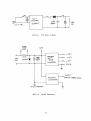
SYNCHRONOUS CONTROLLER. CHOPPER WHEEL DRIVER. AND SYNCHRONOUS DETECTOR
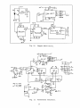
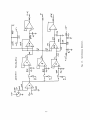
6.1 CHOPPER WHEEL DRIVER
The chopper wheel is driven by a stepper motor, 1.8 degree per
step. The stepper motor driver is an integrated 16 pin dual-in-line IC, type
SAA 1027, (Figure 10). A 500 Hz pulse train is fed to the motor driver to
drive the chopper wheel at 2.5 turns per second. The sync pulse sent by
the phototransistor is shaped by a 74LS221 IC chip and is used to synchronize
the synchronous controller and the reference generator 74LS629.
6.2. THE SYNCHRONOUS CONTROLLER
The synchronous controller as shown in Figure 11 generates the
control signals S, R, and H which switch on and off the synchronous
detector's S channel, R channel, and H channel, respectively. The three
channels extract the sky signal, reference signal , and the hot load
signal from the output of the square-law detector. So the control signal
S, R, and H must keep in synchronism with the chopper wheel.
In one revolution the chopper wheel switches the beam two times
to reference load Tr, two times to hot load Th, and four times to sky Ts;
thus each time lasts 25 steps (45 degrees). The waveforms are shown in
Figure 12.
The waveform of the square-law detector's output shows that
there is a duration of the beam switching, i.e., the beam is not switched
instantly. The reason is that the beam has a non-zero width in the region
that the chopper blade cuts as shown in Figure 14. When the blade is at a
position between a and a', for example, it begins to block off the path of
the sky signal Ts and to reflect the radiation of the reference load Tr.
During this period both the Ts and Tr partially come into the mixer. The
process is similar between the positions b and b' but an opposite process.
Only between the positions a'and b' does the receiver record the radiation
of the reference load Tr. Thus, the intervals aa' and bb' must be cut off
during synchronous detection. That is the purpose of the blanking pulse
(waveform d in Fig. 12). It is necessary to find the width of the
12
+5•
/co
no
130
/3
4.1
is
/4
4
5AA
06
1027
+12v
a;
NoroR
3 ,o S 12
K
H2141
+5"V
(i-8)
Svo
,yz
10i
12
CLIC
74LS
2
> r74LS2Z1
74 L S
1 41A
/1
qv
CL/?
629
IF
—31—nerir
H 7
• 01 pF
Fig. 10. Chopper Wheel Driver.
tO0
•
22o
4
/4
TiV6
SAA
/o2.7
?
ECW
{ . ./..5
3or /Sr 3..taif
3.3K
1.44
+14-*
4
/0
EMr talot
416
8
If
•
A
41 44 C-Zii
+8-
es
8
2.0 ms
"2I
4
4
CZ0eR
Ph
2 '
4 00
rt/
~3 ph
Iraq
0
Fig. 11. Synchronous Controller.
13
//
'K
15
el 11
' '.
,
i i iliv, ,'I 't 11
'
HT
i in'
I II
i
,
1
\ i
1
i ii
'
1 I
i
ii
'I
,
i
—II
)
iiiiiii iii '
11 1 I I
.1
1 \
1
I
1
11 11„11 II
. ,,
q
i.)
it
.
I
1 1
1
I
I
.
i ll
'
v
. I ! '
1
I
t
1
I
I
1
I I
, I
I
1 1
1
I
. 1
I
II
1
1
25"
5.0
(00
75'
125—
/50
175-
200
The waveform of the incident signal chopped by
chopper wheel.
b)
The waveform of the square-law detector output.
c)
Synchronous pulse, generated by phototransistor.
d)
The blanking pulse waveform.
e), f), g) Synchronous detector switching signals.
h)
The driving pulse for the chopper wheel.
Fig. 12. Waveforms of Signals.
14
i
'
Fig. 13. The Motion of the Blade Switches the Beam from the Sky to the
Reference Load and the Square-Law Detector Output Waveform.
BE.4111
Cur —
1
SEC rieN
—
AXi5
ciz
C•
r-2
7-1-1
t-i
Fig. 14. The Angle of the Beam Cut-Section
Opened to the Chopper Wheel Shaft.
15
blanking pulse for the design of synchronous controller. In order to
determine the pulse width of the blanking pulse, it is necessary to determine
the time required for the blade edge to pass entirely through the beam
(Fig. 13). The maximum width or the cut-section of the beam can be found
as
L R1 * W * Sin A * 1/F - 0.269"
, equals to the lens' radius
Where R1 - 1.0"
W = 1.412" , the width of the blade
F - 2.562" , the focal length of the mirror
A = 29.27° , the angle between the normal line of the blade and the
beam axis
Referring to Figure 14, we can find how many steps (or times) it will take
for the blade to pass through such a width. It is equal to the duty Bl of
the blanking pulse.
B1 = A l /1.8°
2 * Sin-(r/R) - 5 steps (- 10 mS)
6.3. SYNCHRONOUS DETECTOR
Figure 15 is a schematic of the synchronous detector. The
output of the square-law detectors fed to the positive input of the OP AMP
A. The inverting input of the OP AMP A is connected to +10 volt DC through
a 100 K ohm resistor. So its output voltage is -10 volts when the input
voltage is zero. When the input voltage is Ei, its output can be given as
2 * Ei -10,000 mV
The output of OP AMP A is fed to three analog switches which are controlled
by three synchronous switching signals S, R, and H, respectively. So that
the sky signal Ts, reference signal Tr, and hot load signal Th are separately
extracted out by those three switches each followed by an integrator. The
integrators' outputs Es, Er, and Eh are fed to two subtractors to obtain
the outputs of R, (S - R) and (H - R) that
R = Er
S - R - 10 * (Es - Er)
H - R - 100 * (Eh - Er)
and Es - 2 * Grcv * (Ts + Tsys) - 10,000 mV
Eh - 2 * Grcv * (Th + Tsys) - 10,000 mV
Er - 2 * Grcv * (Tr + Tsys) - 10,000 mV
16
Fig. 15. Synchronous Detector.
Where Gre y ...............
Ts
Th
.........
.........
Tr
Tsys .........
the gain of the receiver in millivolts/Kelvin
the observed object's temperature in Kelvin
the hot load temperature in Kelvin
the reference load temperature in Kelvin
the effective noise temperature of the receiver
Then we have
S - R — 20 * Grcv * (Ts - Tr)
H - R — 200 * Grcv * (Th - Tr)
R — 2 * Grcv * (Tr + Tsys) -10,000
The temperatures of Th and Tr are exactly controlled at 65°C and
45°C, respectively. So if we adjust the gain Grcv to make the output of
the (H - R) AMP as
H - R — 200 Grcv * (Th - Tr) — 200 Grcv * 65 - 45) — 4000 Grcv — 4000 mV
then the gain of the receiver Grcv = 1 mV/per Kelvin. The output of the
synchronous detector can then be given as
S - R — 20 (Ts - 318) mV
H R — 4000 mV
R = 2 (Tsys + 318) - 10,000 mV
Here we see that the output of (H - R) is a constant of 4000 mV
if the receiver is properly adjusted. The reading of (H - R) can also be
used to check the system synchronization. That is, by changing the Ts
from room temperature to liquid nitrogen temperature, the readings of the
(H - R) should remain constant. If it changes too much (should be less
than 20 mV or 0.1 degree), the system is out of synchronization.
7.
ELEVATION MIRROR DRIVER
The elevation mirror can be either computer controlled or manually
controlled. Figure 16 is the schematic of elevation mirror driver.
7.1.
MIRROR SCANNING DIRECTION CONTROL
The direction of the elevation mirror scanning is controlled by
the potential level of the IC chip SAA 1027 's DIRECTION PIN 3. When it
is high, the mirror will scan in a clockwise (CW) direction. The level is
determined by the state of CW (controlled by computer) and the state of
the J-K flip- flop 74LS109 (controlled by manual). The direction is given
as
Dir CW * Q2 + Q2 * CW
18
r
ISA
!.0
12
pRotn
cpu
6o zavt*
46-
ez
10
"T
/0 0
sr
MM.
100
Zit tit
q
Ti' 114
//- S 2Z
1
t
Cy/.
Plotn CO(',
I
lb
0
/114AP
D/4 .
/.0
/60K 4-3•V
4 fRp
4 SH -fe444/4)
Alo-gat
..44
pe it Wm) 0•144
Fig. 16. Elevation Mirror Driver.
ST11P
plem CPU
IV"
."-A41—
-r.
rAFL, a
47K
3.
a
4441027
Qi
Ts
2d)
4.4!)-
Acvia. 267 171
s Wee Nitre.
ELEVArtaA/ merwi z•nlve.
De
K
§1 COL
4
leV4002
When in manual control mode, no matter whether CW is HIGH or LOW,
each push of the MAN DIR switch will toggle the flip-flop Q2; therefore,
the direction changes. When in the CPU MODE, if Q2 is low (Q2 — 0), the
direction DIR CW. The direction coincides with the computer's command.
If Q2 is high (Q2 — 1), DIR CW. The direction is opposite to the
computer's command. So it is necessary to reset the flip-flop Q2 to zero
when the computer begins to control the direction. This is realized by
the NOT OR gate 74LSO2 . Its inputs are connected to the computer controlled
GZ (go to zenith) and ST (step) and its output is connected to the CLR2 of
flip-flop Q2. Then
CLR2
GZ + ST
Normally, if there is no CPU control command, GZ and ST are both zero.
Then the CLR2 — 1 . When the CPU wants to control the elevation mirror,
go to zenith or step; either CZ or ST gives a positive pulse which will
cause a negative pulse at CLR2
and reset Q2 to zero.
7.2. GO ZENITH CONTROL
The oscillator 74LS629 supplies 50 Hz clock pulses to gate A.
When a positive pulse occurs, either on the computer controlled CPU GZ
line or the manual controlled MAN GZ line, it will set the flip-flop Ql to
HIGH (Ql — 1) which allows the clock pulses pass through gate A and via
the Exclusive OR 74LS86 to the motor driver SAA 1027. When the mirror
arrives at the zenith position, the phototransistor H21A1 sends out a
negative pulse. This pulse is shaped by the monostable mutivibrator
74145221 and be used to reset the flip-flop Ql via the AND gate B, therefore
closing the gate A and stopping the mirror. The other pin of gate B is
connected to manual control STEP switch. When the MAN ST switch is closed,
a negative pulse occurs at the output of gate B and resets Ql. So, if the
mirror is turning on the way to zenith and you push the MAN ST switch, the
mirror will stop. Then each push on the MAN ST switch makes the mirror
move one step (1.8 degree).
8.
INTERFACE AND DATA LINK
The data acquisition and monitor/control interface are realized by
employing a VLBA standard interface card. For details please refer to the
VLBA specification A55001N002-A.
9.
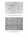
CALIBRATION AND RESULT
When power supply to the system is turned on and the working program
disc is in the computer disc drive, the system will setup automatically.
Normal operation will not occur until the reference load and the hot load
are heated up and stabilized. Check the readings on CRT screen and make
sure the REF TEM is 45 C and the HOT TEM is 65°C and the H - R is 20 K.
The system is then ready to operate. Normally, it will take approximately
20 minutes to warm up depending upon the initial equipment temperature.
20
••
Figure 17 is a chart record of the synchronous detector's analog
outputs S-R and R for different temperature absorbers placed in front of
the elevation mirror.
• •
•
•
.
-
_
•
•
.
—75#1 P-e
qtria-ifiti
(hi
5
-
.
• -
:
•-•;;*
.
.
0
K
-
•••• • •••••••••,••••••••••• ••••• •■••••••
•
.
•
••••••••
-
-
-
:
5b-C, -445-A
_
• ••■••••
:
.
.
-21 k-
••••••••••••••••••••••••••
•
"
"
_
_..:_-77-•-:
•
•
.."
•
••
••
•
•••••• •••• • • • ••••• • • •
••• ••
•
I. •
••• •••••• ••• ••
_. •• •. .
• •• • • • •
••• • ••• ••••• •••• •
••
•••••
•
••
• •••• • •
.7
_
••••••••
-
'.*
*
7
•••• •••
•
.
.
•
••
4f
•
,-
-
•
•••
•
•
'
• •
••.....•.••• • • •
•
••.•
•... •
.:
•_
-77=
•
-.
-
.
-
•
-.-t
_
...__.-
•_
_
_ ._
-- -
- "
_
_
••••••• _
•_ ^ •
--•--
--7.••••
• 77.7
------ • ---
7-7--,.
'"7""
Ito
•..
'.."
•-•-•
-
c AebeKePx
•
_
"
• • •••••••••••••••••••
• ••• • ••• •••••••••••• •••••• • ••••••• • • -
• . •••••••••••••• •
5 IC ----
•
•
-
_ -•
• 777.•._. •
404
c
•• • • -•
•
•
_77
7
•
.7: : •
•- • -
••••••• •• • • ••••••.•••••••••••.••••• •••••• •••••••••••••• •••• •••••• •••••••••• ••••• ••• •
_
_ _ .
..
•••••• • ••
•
:
.
.
•
• .
.
_
•
•
•••
.
•
•
••••••
•••••••• •
•
• • ••• • •
••••• •••••• • ••• •••• • •
•
____.
.
•••••••••• ••••■••••••••••••••••••••••••••••••••••
•
--
•
•
•••• •••••
•••••••• • ••• •• •••••••••• •••••••, • •••
. ••
•
•
- - - — - — -
•
•••• ••••
• •
1-0N.
•
•
•
-•
•-
'
"1.
.7 77
•.
7.-. .
(4. 51Z—Z+6
•••••••••••••.•••••• •
•••••••••••••••••••••••
.
• •
•
•
••••
-
•
4
630itibek
- .-
-77:777:
..
•
••••••••• • .•
-• ' "71
.
. _•
'
:
.._
_
..
•
_ •_.
...=
.___ _
_
°' /%4
••••••••••
-
•
S
.•
:. .: • - -•
_
•----
- •
•-
Fig. 17. The Calibration Result.
21
--- •
••.
,- •
• •- N._ • - •
•
_ • _
'77. 72.77 - -7777_77:-."7:."-.."7"
. '7
•-
10. ACKNOWLEDGEMENTS
The 225 GHz atmospheric receiver system described here was designed
by Dr. S. Weinreb. All the construction and test works were done under his
direction and help from beginning to end. I am grateful to N. Horner for
his assembly of the mixers and triplers. Thanks also go to W. Luckado,
G. Taylor and D. Dillon for their help with fabricating the many components
of the receiver and the measurement systems.
11. REFERENCES
[1] S. Weinreb, "225 GHZ Receiver Test Program," NRAO Internal Memorandum,
April 22, 1986.
[2] J. W. Archer, "Millimeter Wavelengh Frequency Multipliers," IEEE Trans.
Microwave Theory & Tech., vol. MTT-29, no. 6, pp. 552-557, June
1981.
[3] J. W. Archer, "All Solid-State Low-Noise Receivers for 210-240 GHZ,"
IEEE Trans. Microwave Theory & Tech., vol. MTT-30, no 8.,
pp. 1247-1252, August 1982.
[4] J. Silver, "Microwave Antenna Theory and Design," M.I.T. Rad. Lab.
Series, vol. 12, ch. 11, New York: McGraw-Hill, 1984.
[5] Paul F. Goldsmith and Ellen L. Moore, "Gaussian Optics Lens Antennas,"
Microwave Journal, pp. 153-156, July 1984.
[6] A. R. Kerr, R. J. Mattaudh and J.A.Grange "A New Mixer Design for
140-220 GHZ," IEEE Trans. Microwave Theory & Tech., no. 5,
vol. MTT-25, pp. 399-401, May 1977.
[7] M. T. Faber and J. W. Archer, "A Very Low-Noise, Fixed-Tuned Mixer
for 240-270 GHZ," IEEE MTT-S Int. Microwave Symp. Dig.,
pp. 311-314, June 1985.
[8] S. Weinreb, "Square-Law Detector Tests," NRAO Electronics Division
Internal Report No. 214, May 1981.
22
APPENDIX I. Photograph and Schematic of the Square-Law Detector
ewe
/NW .11. caw
4=0
alb
—
Sal.,3
a
)
f••=
34:1./k
G
-4.
. oct2.
Fok..) T"'
1,4EAR
s
ocesas,
lb
/(34c
T-
1■14
•
SI
Sk.c.
/0 0
4.00s-=BIND MINIM
darr
4111111111P
4111111111
_
own.
. .11M•
‘a.a*
e
A.......11\PArri•■■•
C 7
i
A
oc
r-
2E0
23
.411•■
emia
gm.
sogi.
dB.
MIN.
MIND
NNW
ERIN.
...a
.10
4111111,
APPENDIX II.
The Temperature Controller
The temperature controllers are used to heat and control the
0
temperatures of the reference load (45 C) and the hot load (65°C). The
reference load and the hot load are made from a sort of liquid microwave
absorbant. One pound of this absorbant is mixed with 20 milliliters
hardener. Plaster the mixture onto a 9.0-10.5 cm 2 aluminum plate with a
mold to dry. The surface of the absorber is grooved and coated with a
layer of foam which is transparent to the microwave emission. The plate
is heated by a power resistor controlled by the temperature controller.
Figure APII-A is a schematic of the temperature controller.
24
#
/1‹
'
t<
r%
9.09K
/A
200
fati-J2-
/d.co/C
/A,
/0
nionf
ie 0 w•Vit
/A(4 737
C->
-4(
to n4F
APAP it
OUT
{ IN e
tP4 -
VCC
IN •
IN —
OUT
O. J. OR N DUAL IN.UNUPACKAGE
(TOP VIEW)
ALL oP 444P S
y
4 "7/...c 274
/0
/OM •
/044
"012V
B
C
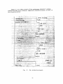
APPENDIX III. 12V Power Supply and DC/DC Converter
1)
Schematic of the 12V Power Supply ........................ APIII-A
2)
Schematic of the DC/DC Converter ........................ APIII-B
2) 12V Power Supply Photograph and Manufacturer Data Sheets
3)
DC/DC Converter Photograph and Manufacturer Data Sheets .
26
APIII-C
APIII-D
APIII-A. 12V Power Supply
CURA
SEA'S
c T
. 0 1 12
2.V
C
int3319
'vi
p 0 we
/000
duF
esv
GEA".
•
q a
rA/v4R rAtK
41.1•11mb
41(W)mist
/ ve ti•rEl?
+12V RETURN
APIII-B. DC/DC Converter
27
FoR erg AfriPS
50 TO 384 WATT - SINGLE OUTPUT
J
witching Regulated Power Supply
• Recognized under IEC 380 safety
standards
II Meets VDE 0806 safety design standards
III Complies with UL 478 and CSA C22.2 154
II Input filter conforms to VDE 0871/6.78
and FCC 20780 Part 15, Subpart J
The EVS family of single output switchers incorporates the latest in switching technology to offer low
Cost, high-performance solutions to your power supply. These efficient, light weight units are available in
5. 12. 15 and 24 VDC versions. Units are designed
and qualified to meet all of the latest required regulatory specifications used throughout the world.
si •
II AC transient suppression
1111 Logic inhibit on many models
R Remote or local sensing on most models
II Cover included with all models
III User selectable 115/230 VAC dual input
111 Overvoltage protection
III Overload protection
III Short circuit protection
Parameter
Conditions
AC Input
47-63 Hz
(consult factory for 400 Hz)
Limits
Parameter
90-132180-250 VAC Oversnoot
(user selectable)
Input Surge Current
See Ordering Information Chart
DC Output
DC Out p ut Adjustment
Within specified AC limits
Load Regulation
No load to full load
Noise and Ripple
DC - 50 MHz
75 mV peak-to-peak
maximum
Hoid-a# Time
Based upon nominal input
voltage and full load
20 ms
Transient Response
50 to 100 0 load change
2°, in 1 0 ms
Efficiency
According to output voltage
70 - 600.
0
-
0 5°.
Peak (cola start)
20A (115 VAC)
40A (220 VAC1
Logic Inhibit Function
(Series EVS-F. G. H. J)
Referenced to ( — I negative
sense terminal
4 5 to 5 5V
Polarity
Either positive. negative
floating
Up to 300 VDC
Soft SI31
Provides input current
limiting at turn-on
Parallel O p eration
Consult factory
• •■••••• •••■••
Provision included for
improved overall regulation
Overload Protection
Long Term Stability
Automatic electronic circuit
Ambient Operating
Temperature
Preset Value
For 8 firs atter 20 min
0 I'.
WUM-0
Built-in fold back
li miting
Short Circuit Protection
-.^ -• - •
. • Limits
.
No voltage spikes on turn-on.
turn-off or power failure
7. 10°.
Line Regulation
mote 'Local Sensing
eries EVS-F. G. H. J1
Conditions
Continuous Duty
Full rating
Derate linearly to 50°o of
full rating at —71 C
Storage Temperature
0 C to 71 C
C
- 50 C
_
20 C to 85 C
••••
OveNoltage Protection
fixed
Quality Control
According to MIL-I-45208
APIII-C. 12V Power Supply Photograph/Manufacturer Data Sheets
28
10 WATTS OF REGULATED 5V, -.±15V;
5V, ±121i; 5V, +12V/-5V
ISOLATED ANALOG & DIGITAL GROUNDS
GENERAL SPECIFICATION
ELECTRICAL
I NPUT
Voltage range .......................... See ordering information
Current
.............................. See ordering information
Filter ......................................... r type
Switching frequency ................. 20 KHZ
POWER
GENERAL
OUTPUT
Voltage, output El & E2 ........... -4- 1°/0 Max. (— 5VDC, 2%
Max.)
output E3 ................... 5VDC, 1% Max.
Voltage Balance. El to E2 ........ ± 0.2% Max. (Tracking. ± 15V
and ±..12V only)
Current ...................................... See ordering information
Voltage limiting (o.v.p). E3 ........ 6.8V
Load Regulation (NL-FL),
El & E2 . . . 0.02%. ± 0.1% Max.
E3 .
0.1%, ± 0.2% Max.
Line Regulation (LL-HL),
-4- 0 02% :•_- 0.1% Max.
El & E2 ...................
E3 . . 0.1%, ± 0.2% Max.
0.02°/0/°C Max.
Temperature Coefficient... .
Initial Warm-up Voltage Drift,
El & E2 . . . 20mV, ± 90mV Max.
E3 . . . 10mV, ± 40mV Max.
Current Limit ......... ................. All outputs constant
current limit protected.
Nair
NOISE
Output Noise Voltage
(All outputs) ........... ................. 1 mV True RMS Max.
15mV p-p. 40mV p-p Max.
Reflected Input Ripple Current . .15mA p-p, 40mA p-p Max.
Common Mode Noise Current . .500/.4 A P-P.
TRANSFER
KOCK MAIRAN SRO 131
.1E ,, ATOR
E.
C,Iipt,
ImpIt Output
0C—OC Convtrter
IRS
AN,OG
SP,
s .L,ERS
C OmM.
Efficiency ............. ............................ >50%
Breakdown Voltage. .. . . .. 500VDC Min.
Isolation (Input to output
& E. .. E2 to E3)
.
Capacitance ................. 50 pf
1099 Min.
Resistance.
:0,RC,LLE
CC
INPw.
ENVIRONMENTAL
,A17
c;LTE
vER,E
ANALo ,
.—
\\D
£2
Operating Temperature Range. .
Storage Temperature Range . . .
25°C to + 71°C
40°C to + 125°C
pcs,TtvE
MECHANICAL
REGu,...vroci
a
E
FIRS
Ahr.
tiT
6401,
s'
DIGITAL
Case Material ............................ Metal
Module size .................................. 2 56" x 3.00" x .75"
COMMO,
GENERAL DESCRIPTION
This new series of 10 Watts Triple Output DC/DC Converter
features isolation between the 'Analog outputs and the
Digital output as recommended by many A-D/D-A Converter manufacturers for the purpose of inhibiting Digital
interference in the Analog section and eliminating system
ground-loop problems.
All models feature internal r input filters to minimize reflected input ripple voltage, output current limiting with
automatic restart when the short circuit is removed and
input protection against accidental application of reverse
voltage polarity. Ferrite pot-core transformer and 6 sided
electrostatic shielding after inherent shielding against radiated EMI/RFI.
The Analog outputs (I- 15VDC, 12VDC) are Dual Tracking and balanced within 0.2%.
APIII - D. DC/DC Converter Photograph/Manufacturer Data Sheets
29
vilEDC INPUT VOLTAGE .-.
AMOMINAL /RANGE
5V/4.5V to 5.5V
_I
= OUTPUT l'AVOLTAGE S CURRENT
5V 41 1
12V/10V to 14V
24V120V to 28V
28V/24V to 32V
48V/42V to 56V
5V/45V to 5.5V
12V/10V to 14V
it: 15V
0
,
. -130N PUT CURRENT
--410 LOAD/FULL LOAD
± 165 mA
it 12V az it 200 mA
932
933
934
6.8 VDC
on
935
936
937
938
5V out
- 5V at 100 mA
,
939
940
50 mA/0.66 A
60 mA/0.39 A
400 mA/3.5 A
140 mA/1.4 A
55 mA/0.70 A
50 mA/0.62 A
60 mA/0.37 A
5V @, 1A
+ 12V i 300 mA
*PRICE , .
"j11.24)
14110A0DEL.
? UMBER
931
400 mA13.7 A
140 mA/1.5 A
55 mA/0.75 A
50 mA/0.66 A
50 mA/0.39 A
400 mAt3.7 A
140 mA/1.5 A
55 mA/0.75 A
A
5V @ 1 A
24V/20V to 28V
28V/24V to 32V
48V/42V to 56V
5V14.5V to 5.5V
12V/10V to 14V
24V120V to 28V
28V124V to 32V
48V/42V to 56V
fiCOUTPUT .'.'---v-...1:1.V.P. '
941
942
943
944
945
CASE/PIN CONFIGURATIONS
.800
20.32
.700
17.78 1
.25
MiN
6. 3
NOTE 3
.300
7.62
65-
.500
42.70
.200
5.08
--21-
-0-0- -o o o
15 1 4 13
17 16
2.50
63.5
NOTE 4
I A/
L1.000
25.40
1.25
3.00
76.2
31.7
12
-0-
A00
7.6
41 0.16
1.50
38.1 ---41
2 .56
65.0
FUNCTION
mODELI PIN
I
4 iNPUT
•
:,14 ENSION.5 SM.-J.4N IN
2
-INPUT
931
3
+ E i OUTPUT
Tofftu
4
I:
945
5
- Ez OUTPUT
6
+ E 3 OUTPUT
2
x XX
COMMON
040
IN
MY
,
z 0 C 2,X xx%
DiA
3
PINS
4
MOUNTING INSERTS • 4 -40x.
02
.
FE
DP
(3 COMMON
152 WILL DRIVE. CANTON. MA 02021 TWX: 710-348-0200 TELEPHONE (617) 828-6216
27
APIII-D (continued)
30
APPENDIX IV. The Connector Wirings
1)
Parallel I/O Connector
APIV-A
2)
Serial I/O Connector ..................................
APIV-B
3)
Connector on the Receiver Component Plate
APIV-C
4)
Connector on the Receiver Cover .
APIV-D
5)
Power Supply and Data Link Connector Jl .............. ... . APIV-E
6)
Receiver to Elevation Mirror Connector J2
7)
Monitor Connector J3 ................................. . APIV-G
31
. APIV-F
r
H
14e.
(,)
MUM
e opo(Dc)coge
sc:) c)c)(-D 6®©o@egcom
0®
oggighooe
>
\ Pi o
ci e l e
o o
TiOi
cet 2
APIV-A. Parallel I/O Connector
e
Z
\00
0 0 ® 0 00() OC)
St )
°
® C)0
C) r
Pg)
To Socket 3
APIV-B. Serial I/O Connector
32
+12V -4
RE rtlIZA/
1,
FoR rF A M P. "s
LED
6-1
‘
6A1D
0 g
0 ©
0(410
4)
5"v S Tii H rev R Iran
v
IGuNA/ 5Y-tvc,
®000
0 al.A0
tiO
OCR
ciloPPE& 5Q-4414,
v
0 ur
APIV-C. Connector on the Receiver Component Plate
7;ur Ti
.
5-1?
mixl?
co @®@)ooto,00300
c)c ec@coe@ep@_)@oc)&eyeat
p
6 to1N VSup isup Z4II6L SPARE
1
APIV-D. Connector on the Receiver Cover
33
31-/
R
R _
DA7:4
tact', YE"?
FROY:
coritiECTOR
100Wff&
TO:
jfi
st)
CONNECTOR
TYPE
CABLE IDENTIFICATION
ASSEMBLER
DATE
FROM
_COMB.
TO
PIN
COLOR
PIN
4
PURPOSE
DA 7;1
IN/ r
4 t 2v
1
1
it
c
I
o
pArA
ic‘i
gAID
F
l2v
c
G ArD
I?
I
/2
RE rim/N./
•
w
°Ann> -
.
C Al 13 1
71
Atilliabl.
0 sal"
1
•
46 Gs 411
141111111OF
1
1
I
41
ill
I
•
Ala. T. LINCOLN LABOI:AT01:1*
APIV-E. Power Supply and Data
34
Link
Connector JI
Ci 7; E AL
RECE(1,*
33/06
CONN ECTOR
—.2 (5
TO:
CONN ECTOR
CABLE IDENTIFICATION
TYPE
ASSEMBLER
FROM
PIN
DATE
COND.
COLOR
TO
PIN
PURPOSE
A
*12"
&IOWA/
Aiorm Or
Rg.D
otV,IVE
Yi44oto
43
gREEA/
141147o
Amoft
LEI>
povve ifs-v
LED 6A/D
131ve
pvapLE
T. Litvrni LAttoi:Aronv
APIV-F. Receiver to Elevation Mirror Connector J2
35
^
golv Irso
FRO:
CONN ECTOR
CORD
DooA--rop
ECE/VE1
GLEhAL LeLAI!;‘7,
ts, E
CoArAt ec
R
S a to —
20-235
TO:
CONN ECTOR
TYPE
CABLE IDENTIFICATION
ASSEMBLER
DATE
FROM
PIN
COND.
COLOR
TO
PIN
PURPOSE
Alt1l2o X
.,d
3 AEC
CtioppeR Srivc
C
Al 4ArtiA 4 sT p Aro
o&
e I
L.
.
-if
0
a
H— A
itioAfirM
j.
Alo At eirio
1-.
Ai tikk CU AREN 7-
I
(9'
/40194V, re9t
CHASSIS TER ef AI a ri1RE
.4111114111bk,
11d
6 — ii
7
i=g=
Ok .
le__
I
•
*
Os
6"tp
H AAtu AZ Co ZiAlt7V c7p4 ---02
0 f• 01,
-mmoupw-
piAvu AL 45 7-5P Arai, enh
X
/14A/sit/ d14 D f le e orIDA/ C rn4 --*
il
gf
"'
—rap
i
L. Pt:PA/EA
64/7—`
0
ro A TA 0 Ur LE D Af 0 Ae,Ter
..9"
coisirRo4 a TR 4 E R Co #4 AfoN
_
M.I.T. LINCOLN LApOhA TORY
APIV-G. Monitor Connector J3
36
APPENDIX V. The Layout and Wiring of the Wire-Wrap Card
1)
The Layout and Wiring of Wire-Wrap Card ............ ..... . APV-A
2)
The Socket Wiring . .
3)
The RS-485 To/From RS-232 Link
APV-B
(includes chips 2, 3, 6, 7 and 8)
APV-C
The Control and Monitor Data Link
(includes chips 4 and 9, and the VLBA M/C card)
APV-D
The Elevation Mirror Driver
(includes chips 12-14, 16-19 and 26 .
6)
The Chopper Wheel Driver
(includes chips 22, 23, 24 and 27)
7)
Fig. 16
. Fig. 10
The Synchronous Controller
(includes chips 23-25 and 27-30)
37
Fig. 11
1311
5
N
+15v
109
S0CKET?
6 ISM 1 3 a
a 345 7
4 SN74LIMI
/6
.+5.1
V
•■•■■••••••
5'
7
log
SOCKT
4
2 3 4 56 7 A.
4 3
4,ai, nil
itNik
•••••■•••■■■
I 8r-
4 $ 312 ii so $7
3 744 S 86
i 2 34 5 T
1
I__
1
16 1 5' 1 41 0 u Wq
L
2 74 S 00.9
/ 2 34 5G 78
•••■••■
1-4
47oc
1
S
o p 4{2,V
1
14 13 12 / 0 98
74L- 08
I 2 3 4 5' 67
1
/00
*A al-AA- 0-3
IS- 4 ,a 2 ,/
C Sii#4102 7 sb
5-12
•Ip
u
:34 54 6 10.90
*AP
74ise2I
6
# -
1T
15'ot
log
-
L1Ir
I
/s-,4 1 3 a/.
z
7 74L.5 G29
toK
100
+5"
2 3 5-‘7..
/2 II /, CI
V
+5"'
._
J
1.7,
4
,
3
a
25 7445
[610 2 /
24 74L5 !I
11/2 8
45. 1,
ST0P
4 1/ 0. 3 12•39
22 74 1.5 221
427 63-18
IOC
APV-A. The Layout and Wiring of Wire-Wrap Card
g
LLL,a is /69
01. Soc c r3
t_4_21 .ty. a
9 S/v7445378
4 IF I
6 2
38
2
8 SN7St74
4 cl
6
74LS 74_
/ 2 5' 3 74 6
2
ts-v•
1
ittli
to 1615'14 /3 u 9
V
ts-v
4.1_
•
,
3
7
1
4 13/2 ' (0 9 A
3 0 74% 02
2 4 5 6.
-
/ 2 /4 /3
I
•411$
S' 4, 7
29L 74Ls/6!.1
47,"
1.---'
MK
4
74 L5C2`1
ii /
27
In
FIT
/6 / 5- ,0
31
i
cw
a
CI4P LED
1 GE.-tv,
r
SyAtH
7
> , 74 01)7'-
d
AiDA,,r0F\
/1
ZrE
kcw
3
STR ieERIcieftv
Gc zedvirri
Vcc
1 3
C.A 7
CIVI)
ii
0
, Ai S
7_1LS:1f
I/
i'otir
n
,
Pi(Igoi,/
xivri(-)
"'P
12
1.4
4
/4 J
cae•
16
X
filr(4-)
Ct/C-
.3
im•MNIVI
I AR--
iIc
.11
' 1APV-B. The Socket Wiring
39
C
3
c-,01
7
•
WD
XAttr
7
Ii
-I 5-v
(10
ao
3
3
tr)
tr;
1,.
i'-
81
8
/00
11.
1 -
X ARr
MSG
DATA our
v
1CV(1-)
GA/ D
keir (÷)
s
i -
4
-44
—
24 4 - °sr
/2
IC
/0
20
25
-<12
-‹
1
P
-<21
S
p2
APV-C. The RS-485 To/From RS-232 Link
To / rofil 8 5 2 32 LIA/K
v66Esr,r) q.5 - 485-
DO-25P—comv.
RS 232
-
7
A
Xrre
/./ 4 Z
.7)
4 I
..5
4 3
H
A
C4)
)
RCV
41 EA/6
37
c—)
20
(.+ )
K
35
gA 6
,
'""
'
4 ; 7
k iz,
I
El
1
c1
3
1....
1
1'0
5
,
1
- -2 A4 1,
5
D z: V.
(9
-j
. ; 1r
1- t2
vLem
/1
t
3
rn
CAAD
Dtal.
Jib
DEV ACK,vow-e-E
•
3
33
ccevrtRol
•3Z
7
•
z
31
061000,
A io
AAtz,
Drn v
oo *lb tc
..e nnv/K --
cH4Ae.
cnroo
cm env tte
••
••
7
••
7H
oL
1 L
2L
jL
/8
ig
20
B
221
23
24
.2 5
39
I
S'
(t, L
V /rn A
ar—
—
TC
/CV 1;
VSup.
o.S V /v
.2 5
Z
1
.
\rt
A
Pviv/DEC
7L
so i
I
I
/
I
s-v s-•
CC lvArSbCrDAt viz-E.
I
APV-D. The Control and Monitor Data Link
41
.
01
/C
C4P,D