1
Student Papers in
Computer Architecture, 2006
Aron Andersson and
Ola Ågren (editors)
Technical report, 2006
UMINF 06.32
ISSN 0348-0542
D EPARTMENT OF C OMPUTING S CIENCE
U MEÅ U NIVERSITY
SE-901 87 U MEÅ
S WEDEN
ii
C OPYRIGHT C 2006
UMINF 06.32
ISSN 0348-0542
iii
Umeå’s Tenth Student
Workshop in Computer
Architecture
This book is the proceeding from Umeå’s Tenth Student Workshop in Computer Architecture. It contains a collection of short technical articles about past and present
processors, medias, busses and protocols. The articles have been written by the students of the autumn 2006 offering of the course in Computer Architecture.
Introduction
This is the proceeding of the ten year anniversary Student Workshop in Computer Architecture. The first year it was web based only, but the following nine years we have
been blessed (some might say cursed) with oral presentations as well. In the year 2000
we gave up on the web based proceedings and printed a book instead. The combination of both oral presentations and a printed proceeding has been such a success that
we have continued in that manner ever since.
The structure of the book has changed only slightly since last year, mainly because
of fewer non-processor submissions. This proceeding is thinner than ever before —
due to a declining student enrolment — but the material is as good as ever and well
worth reading. With this note we leave you to it.
September 2006
Program committee: Andersson and Ågren
A Note on Trademarks and Registered Trademarks
All brand names or product names referred to in this work are the property of their
respective holders, and their use here should not be seen as a violation of current trademark laws. The program committee takes no responsibility for uses of such names
without further references.
Student Papers in Computer Architecture, 2006
iv
September 29, 2006
Andersson and Ågren (editors)
CONTENTS
v
Contents
I Processors
1
1 ARM7TDMI
Anders Rånes
3
2 DEC Alpha 21164
Michael Knutsson and Thomas Knutsson
7
3 Intel 386 DX
Henric Granberg and Henrik Nyberg
11
4 Intel Itanium
Jonas Eriksson
17
5 MOS Technology 6502
Tomas Sjödin and Johan Jonsson
21
6 Motorola 68000
Daniel Ekström
25
7 PIC 16F84
Omas Jakobsson and Martin Nilsson
29
8 PowerPC 750
Kjell Winblad and Anders Hansson
33
9 PowerPC G5
Niclas Hellberg and Johan Svedberg
39
10 Sun UltraSPARC IV
Mikael Jonsén and Lenny Nilsson
43
11 Transmeta Crusoe
Robert Thelin
47
12 ZiLOG Z80
Richard Nordenskjöld and Håkan Fors Nilsson
53
Student Papers in Computer Architecture, 2006
vi
CONTENTS
II Media, Busses and Systems
57
13 CD, CD-R & CD-RW
Anders Berggren
59
14 DVD
Lovisa Pettersson and Sara Johansson
63
15 FireWire
Magnus Larsson and John Talling
67
16 Nintendo DS
David Grundberg and Tommy Jonsson
71
17 USB - Universal Serial Bus
Marcus Granström, Petter Olofsson
75
List of Authors
79
September 29, 2006
Andersson and Ågren (editors)
1
Part I
Processors
Student Papers in Computer Architecture, 2006
2
September 29, 2006
Andersson and Ågren (editors)
A NDERS R ÅNES
3
1. ARM7TDMI
1.1 Introduction
The ARM7TDMI is a general purpose 32-bit microprocessor. It’s based on the RISC
architecture but not as heavily as for example the MIPS processor. To support the needs
of the many systems that use the ARM7TDMI and the ARM family in general, some
ideas from the CISC architecture have been implemented to reduce code size, which
is of great importance to small battery driven systems. It was released in 1995 and its
core is very similar to its predecessor ARM6’s core, however it has many extentions
which, until its release, no other ARM processor had [1, 3]:
•
•
•
•
The ’Thumb’ 16-bit instruction set.
JTAG Debug Module which controls the scan chains.
The EmbeddedICE debugging hardware support.
64-bit results in multiplication.
These four features stand for, in order, the letters T, D, M and I in the processor name.
It also incorporates all the key traits general to all ARM processors which have evolved
since the ARM1 in 1985 [3]:
• Fixed length 32-bit ARM instructions.
• Load-Store architecture which only allows load, store and swap operations to
access data from the memory.
• Conditional execution of all instructions.
• The combining of an ALU operation with a shift operation in a single clockcycle.
1.1.1 ARM family history
The company that developed the first ARM was Acorn Computers Ltd. It had previously developed a highly regarded and very popular microcomputer for the BBC1 .
When designing its successor several commercial microprocessors were considered but
the CISC processors in 1983 were even slower than the contemporary standard memory parts. They were lacking in so many areas where the BBC micro had excelled,
so they came to the conclusion that they had to build their own microprocessor. Such
endeavours had cost the CISC producers several houndreds of man-years to engineer
a design, something Acorn simply could not afford. They had to manufacture a better
processor with a fraction of the design effort and with no previous experience in custom
chip design.
It seemed impossible until they found a paper from Berkeley University about a
RISC processor which had been designed by a few post-gratuate students in under a
year and still was competitive with the leading commercial microprocessors. Many
aspects of this microprocessor were adopted and the Acorn RISC Machine 1 was born.
It was the first commercial RISC processor. In 1990 the company Advanced RISC
1 British
Broadcasting Corp.
Student Papers in Computer Architecture, 2006
4
CHAPTER 1. ARM7TDMI
Machine was founded to expand the use of ARM processors outside of Acorn’s own
products. From then on the acronym ARM stood for Advanced RISC Machine, just
like the new company which was developing and marketing it [3].
1.2 Overview
Here follows an overview of some of the most important system traits of the ARM7TDMI;
some implementations are also covered.
1.2.1 Instruction formats
The ARM7TDMI features two operating states: the ARM 32-bit instruction state and
the Thumb 16-bit instruction state. Switching between them is done with the BX instruction which branches and sets the T-bit in the CPSR2 indicating Thumb-mode.
Switching between modes does not alter the content of the registers, r0-r7 in Thumbmode are the same registers as r0-r7 in ARM-mode. The Thumb instruction set is a
subset of the most commonly used 32-bit ARM-instructions [3].
In ARM-mode data processing instructions use three adresses, two source adresses
and one result register whereas in Thumb-mode one of the source registers is also the
result register. All instructions in ARM-mode can be set as conditional; this feature
does not exist in Thumb-mode where only branches can be conditional. As the instructions in Thumb-mode are only 16-bits, a branch and link has very limited range. This
is solved by combining two operations giving it a 22-bit PC-relative offset. This isn’t a
problem in ARM-mode where the standard branch and link PC-relative offset is 24 bits.
Another feature not available in Thumb-mode is the 64-bit result multiplication which
in ARM-mode use two 32-bit result registers whos concatination is the 64-bit result.
When the processor is in Thumb-mode the Thumb instructions get translated to their
corresponding 32-bit ARM instruction without performance loss [1, 3].
1.2.2 Registers
The ARM7TDMI has 37 registers, these consist of 31 general-purpose 32-bit registers
and 6 status registers. However in normal execution mode only 16 general-purpose and
one or two status registers are available. Interrupts, for example, take the processor into
another operating mode where other registers are also available and, in the example, reserved for interrupt handling. In Thumb-state however, only 11 32-bit registers and one
status register are available. Access to the other registers is restricted, however special
versions of the MOV, CMP and ADD operations can access them in some ways [1].
2 CPSR
stands for “Current Program Status Register” and is the main status register.
September 29, 2006
Andersson and Ågren (editors)
A NDERS R ÅNES
5
1.2.3 Implementations
The ARM family can be found in all sorts of products from small embedded solutions
such as smartcards with flash memory to large products like spaceship avionics.3 But
the biggest category is mobile systems such as smartphones, PDAs, personal media
players, personal GPSs, portable gaming devices and normal mobile phones. Over
75 % of all devices in the mobile systems market are ARM powered. The ARM7TDMI
can be found mainly in mobile systems for which it has been designed, with low power
consumption and high code density, but also printers and networking hardware. Some
of the more famous include:
• Members of the Apple iPod family.
• CCTV network cameras.
• Nintendo Gameboy Advance SP.
Most mobile systems and low power devices today however are based on newer versions of the ARM core such as the ARM9, ARM11 and Intel XScale [2].
1.3 Memory
Memory in the ARM7TDMI is viewed as a linear array of bytes. Data is stored in 32-bit
words, 16-bit halfwords and 8-bit bytes. Words are aligned on 4 byte boundaries and
halfwords on even byte boundaries. The ARM7TDMI can be configured to use ’bigendian’ memory organization but ’little-endian’ is the default setting. The standard
ARM7TDMI core carries no on-chip cache. There are however CPU chips, aimed at
higher performance applications, where the core shares the silicon area with cache such
as the ARM700 with an 8 KB cache holding both instructions and data [3].
1.3.1 Bus
For accessing the memory, be it a cache or the main memory, ARM7TDMI uses a
von Neumann type 32-bit unified bus for both instructions and data. As previously
noted, only load, store and swap operations can access data from the memory through
the bus [1].
1.4 Pipeline
A 3-stage pipeline is used in the ARM7TDMI. All instructions are executed in the
following steps:
1. Fetch
2. Decode
3. Execute
3 SpaceShipOne, winner of the Ansari X-prize in 2004, carries avionics powered by an ARM729T Processor [2, 4].
Student Papers in Computer Architecture, 2006
6
CHAPTER 1. ARM7TDMI
In the fetch step the instruction is fetched from the memory either as a 32-bit ARM
instruction or as a 16-bit Thumb instruction. In the decode step the first action is to
decompress the instruction if it’s in the Thumb format. The second action is decoding
the registers used in the instruction. In the execute step registers are read from the
register bank, ALU and shift operations are performed and lastly registers are written
back to the register bank [1].
1.5 Performance
The ARM7TDMI core consists of 74209 transistors on a 5 mm2 silicon chip. It has
a variable clock frequency of up to 40 MHz. When running standard ARM 32-bit
instructions the execution speed is 36 MIPS. It draws at most 80 mW which concludes
an instruction to power ratio of 450 MIPS/W.
Thumb code is normally only 65 % the size of the same code in 32-bit ARM instructions and runs 160 % faster than ARM instructions running from a 16-bit memory
system. This makes it ideal for running on systems low on memory, which can be
viewed as a performance edge on certain systems [3].
1.6 References
[1] ARM LTD. ARM7TDMI Technical Reference Manual, r4p1 ed., Nov. 1, 2004.
Also available at http://www.arm.com/pdfs/DDI0210C_7tdmi_r4p1_trm.pdf.
[2] ARM LTD. ARM. Web site, Sept. 27, 2006. http://www.arm.com, date visited
given.
[3] F URBER , S. ARM System Architecture. Addison-Wesley, 1996.
[4] X P RIZE F OUNDATION.
Ansari X Prize.
Web page, Sept. 27, 2006.
http://www.xprize.org/xprizes/ansari_x_prize.html, date visited given.
September 29, 2006
Andersson and Ågren (editors)
M ICHAEL K NUTSSON AND T HOMAS K NUTSSON
7
2. DEC Alpha 21164
2.1 Introduction
The DEC Alpha 21164 was released on the 19th of September 1994 and is also known
as the EV5. Its predecessors were the EV45 (DEC Alpha 21064A) which the EV5
based its core on. The model name 21164 stands for that it was thought to be a processor of the 21st century, the 1 for it being the second generation processor of its type
(where 21064 was the first) and the last two digits implied that it was a 64-bit CPU [1].
One specific feature of the EV5 was considered revolutionary; it was the first microprocessor to have a large secondary cache on chip [7].
As for operating systems the processor supports [2]:
• Microsoft Windows NT
• OSF/1
• OpenVMS
2.2 Processor overview
Here a thorough overview of the processor will be given. This includes the different
parts and how they work together.
The DEC Alpha 21164 is a 64-bit processor based on the RISC architecture [3].
RISC is an acronym for Reduced Instruction Set Computer, an instruction set that has
more or less been a standard since 1982 [4].
In the processor, registers are of 64-bit length and all the instructions of 32-bit
length. Since the DEC Alpha 21164 is of a load and store architecture all data manipulation is done between registers. It’s able to issue four instructions or less each clock
cycle [3].
2.2.1 Components of the processor
The processor can be broken down into the following major components. These components will be described further in the upcoming sections, note that these abbreviations will be used while mentioning the components [3].
•
•
•
•
•
•
•
•
•
The IBox, which is the instruction fetch/decode unit and branch unit.
The Ebox, which is the integer execution unit.
The Fbox, which is the floating-point execution unit.
The Mbox, which is the memory address translation unit.
The Cbox, which is the cache control and bus interface unit.
The Dcache, which is the data cache.
The Icache, which is the instruction cache.
The Scache, which is the second-level cache.
The Bcache, which is the optional external cache.
Student Papers in Computer Architecture, 2006
8
CHAPTER 2. DEC ALPHA 21164
2.2.2 Ibox
Simply said the Ibox manages all the instructions that are sent to the Ebox, Fbox and
Mbox. More precisely it handles the execution order and makes sure that only an
instruction with available resources is being executed [3].
To manage the execution order described above, the Ibox forms groups of four
instructions. It checks the available resources for the first four instructions, if all has
the required resources then they’re all executed. If not it only issues instructions up to
the one that doesn’t have the required resources. The Ibox doesn’t continue to the next
group until all of the four instructions in the current group have been issued. This is to
keep the instruction issue order [3].
To predict the outcome of a branch instruction the Ibox has a prediction logic unit.
If a branch instruction is issued the Ibox looks in the Icache, which for every branch
instruction has a 2-bit history value. This value represents the outcome state of that
instruction [2].
2.2.3 Ebox
This unit is used by the processor for handling integers. Important integer operations
that are supported by the Ebox include but are not limited to [3]:
•
•
•
•
Addition
Multiplication
Bit manipulation
Barrel shifting, a process to shift the order of bits in a cyclic manner [5].
The Ebox has two integer pipelines, which allows it to perform two separate integer
operations in one cycle [3].
Furthermore the Ebox includes a 64-bit integer register file, also knows as the IRF
with 40 entries. It contains the 32 integer registers which is used within the Alpha
architecture [3].
2.2.4 Fbox
To calculate with floating-point values the processor utilizes the Fbox. It can handle
the following formats [3]:
•
•
•
•
Longword integer format in floating-point unit
Quadword integer format in floating-point unit
Two IEEE floating-point formats
Three VAX floating-point formats
Like the Ebox the Fbox has a register file called the floating-point register file
(FRF) [3].
September 29, 2006
Andersson and Ågren (editors)
M ICHAEL K NUTSSON AND T HOMAS K NUTSSON
9
2.2.5 Mbox
The main feature of the Mbox is to translate virtual memory addresses into physical
memory addresses. It contains the following components [3]:
• Data translation buffer
• Miss address file
• Write buffer address file
Two or fewer virtual memory addresses are received every cycle from the Ebox. As
a response the Mbox uses the data translation buffer in order to find the corresponding
physical memory address [3].
2.3 Cbox
The Cbox is the unit in the 21164 that handles the caches that hold information about
data, i.e. the caches other than the Icache (which is handled by the Ibox). In the
following sections the purposes of the different data caches, which the Cbox handles,
will be described [3].
2.3.1 Dcache
The Dcache, which is 8 kilobytes large, is the primary data cache with a block size of
32 bytes [3].
2.3.2 Scache
The Scache, which has a size of 96 kilobytes, holds information about both instructions and data. That is due to it being the secondary cache for both the Icache and
the Dcache. It’s 3-way set associative, which means that it can store entries in three
different places [6]. Block size is either 32 bytes or 64 bytes depending on what block
mode it operates in [3].
2.3.3 Bcache
The Bcache is an optional external cache, which can handle cache sizes of 1, 2, 4, 8,
16, 32 and 64 megabytes [3].
2.4 Pipelining
The DEC Alpha 21164 is a pipelined processor. It has 7 stages of pipelining for memory and integer operations. Where the floating-point operations have 9 stages. The
Ibox always handles the first four stages. As for the last stages it ranges between the
Ebox, the Fbox, the Mbox and the Cbox [3].
Student Papers in Computer Architecture, 2006
10
CHAPTER 2. DEC ALPHA 21164
2.5 Performance
Depending on the clock speed the EV5 has the performance according to Table 2.1.
Table 2.1: Performance specification
Speed
SPECint95 SPECfp95 BIPS
600 MHz
18.0
27.0
2.4
500 MHz
15.4
21.1
2.0
433 MHZ
13.3
18.3
1.7
366 MHz
11.3
15.4
1.5
2.6 References
[1] B OLOTOFF , P. V. Alpha: The history in facts and comments. Web page, Mar. 19,
2006. http://www.alasir.com/alpha/alpha_history.html.
[2] D IGITAL E QUIPMENT C ORPORATION.
Alpha 21164 Microprocessor Data Sheet, July 1996.
Also available at ftp://ftp.compaq.com/pub/products/software/alpha-tools/documentation/archive/21164/ec-qaepd-te_21164_data_sheet.pdf.
[3] D IGITAL E QUIPMENT C ORPORATION. Alpha 21164 Microprocessor Hardware
Reference Manual, July 1996.
Also available at ftp://ftp.compaq.com/pub/products/software/alpha-tools/documentation/archive/21164/ec-qaeqd-te_21164_hrm.pdf.
[4] PATTERSON , D. A., AND H ENNESSY, J. L. Computer Organization & Design:
the Hardware/Software Interface, third ed. Morgan Kaufmann Publishers, Inc.,
San Francisco, California, 2005.
[5] W IKIPEDIA.
Barrel
shifter.
Web
page,
Sept.
17,
2006.
17,
2006.
17,
2006.
http://en.wikipedia.org/wiki/Barrel_shifter, date visited given.
[6] W IKIPEDIA.
CPU
Cache.
Web
page,
Sept.
http://en.wikipedia.org/wiki/CPU_cache, date visited given.
[7] W IKIPEDIA.
DEC
Alpha.
Web
page,
Sept.
http://en.wikipedia.org/wiki/DEC_Alpha, date visited given.
September 29, 2006
Andersson and Ågren (editors)
H ENRIC G RANBERG AND H ENRIK N YBERG
11
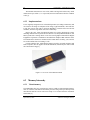
3. Intel 386 DX
3.1 Introduction
Figure 3.1: Front and back of an Intel 386 DX processor
IA-32 Intel Architecture has been at the forefront of the computer revolution and is today the preferred computer architecture, as measured by
computers in use and the total computing power available in the world.
– Intel Corp
The Intel 386 DX was first released in 1985 and had a core frequency of 20 MHz,
followed by models with up to 33 MHz. The new features introduced by the Intel 386 DX were: 32-bit registers and addressing, segmented and flat memory models,
paging and support for parallel stages. These features will be covered more thoroughly
in the following sections [3].
Later, a budget version, with a limited 24-bit address bus, was released under the
name Intel 386 SX [1]. However, this paper only concerns the DX variant . Hereafter
the Intel 386 DX will be referred to as the processor.
3.2 Parallel stages
As stated in [2] the processor has six parallel pipeline stages which are summarized
below:
Bus interface unit — communicates with memory and I/O
Code prefetch unit — fetches object code from the bus interface unit
Instruction decode unit — translates object code into microcode
Execution unit — executes the microcode instructions
Segment unit — translates logical addresses to linear addresses.
Paging unit — translates linear addresses to physical addresses
Student Papers in Computer Architecture, 2006
12
CHAPTER 3. INTEL 386 DX
3.3 Operating modes
The processor can operate in two modes. These are the Protected Mode and the Realaddress mode. The protected mode is the main mode of the processor providing the
best performance and capability. In this mode programs for the 8086 processor can
be executed by using the virtual 8086-mode which however is not a real mode of
operation. The real-address mode is basically a mode providing an environment, of
that of the 8086 processor, with some extensions [3, 2].
3.4 Registers
The processor has eight general-purpose data registers, six segment registers, five
control registers, the EFLAGS register and the EIP register. The ones mentioned are
the basic registers, and there are also other registers but their purpose is not explained
in this paper [3, 4].
3.4.1 General-purpose data registers
The eight general-purpose data registers are all 32-bit registers and are used for holding
operands in calculations and memory pointers, see [3]. The general-purpose data registers inspite of the name have some special tasks, and many instructions use specific
registers for their operands [3]. A summary of the normal usage of these registers is
shown below:
EAX — Accumulator. Used for storing operands and results
EBX — Pointer to data in the DS segment
ECX — Loop and string counter
EDX — I/O pointer
ESI — Source pointer for string operations
EDI — Destination pointer for string operations
EBP — Pointer to data on the stack
ESP — Pointer to the top of the stack
For compatibility the lower 16 bits of the general-purpose data registers can be used
exactly as the registers on the 8086 processor [3].
3.4.2 Segment registers
The six 16-bit segment registers, named CS, DS, SS, ES, FS, GS hold pointers to
memory segments [3]. How the memory is structured and accessed is covered in Section 3.5.
September 29, 2006
Andersson and Ågren (editors)
H ENRIC G RANBERG AND H ENRIK N YBERG
13
3.4.3 Control registers
The five control registers, CR0 through CR4 are used to control the operating mode of
the processor [4].
3.4.4 EFLAGS register
The EFLAGS register is a 32-bit register where 14 bits are reserved and are not to be
used by programs. The other bits can be divided into three groups: status flags, system
flags and a control flag [3].
The status flags show information about the results from arithmetic operations. For
example there is one flag indicating that the operation has overflowed and another
flag indicating whether the result of an operation is positive or negative. The system
flags control some of the behaviours of the processor, for instance I/O, debugging and
interrupts. The virtual 8086 mode can be toggled with one of the system flags [3].
The remaining flag is the DF flag which controls how strings are processed. If this
flag is set, instructions processing strings will work from the highest address to the
lowest [3].
3.4.5 EIP register
The EIP register holds an offset to the next instruction in the current code segment.
Software cannot write to or read from the EIP register explicitly, it has to use the
instructions that modify program flow like the instructions CALL, RET or the various
jump instructions [3].
3.5 Protected mode memory organization
In Protected mode, the full 32-bit addressing capability of the processor is available,
providing a 32-bit address space. In this mode two separate facilities are available for
the operating system to use: segmentation and paging.
3.5.1 Segmentation
The segmentation mechanism is used to divide the linear address space into separate
segments, with different levels of protection, holding the stack, code and data for the
running tasks. They can also contain different system data structures, although they are
not within the scope of this paper. The processor will enforce the boundaries of these
segments, allowing the tasks running on the processor to run without interference from
other tasks. Other restrictions can also be put on the segments, such as making them
read only [4].
To address memory within a segment, a logical address is required, which consists
of both a segment selector and an offset into the segment. A segment selector consists
of an offset into a table of descriptors (such as the GDT or LDT1 ), as well as some
1 Global
Descriptor Table or Local Descriptor Table
Student Papers in Computer Architecture, 2006
14
CHAPTER 3. INTEL 386 DX
other information. These descriptors contain information about the segment, such as
the segments base address in the linear address space, the size of it and its access rights.
To locate a byte within a segment, the offset part of the logical address is added to the
base address of the segment [4].
The 16-bit segment selectors contained within the segment registers determine
which segment should be addressed when the processor performs an operation. For
example, when the processor needs to fetch a new instruction for execution, it looks
for the instruction at the logical address provided by the segment register CS, with the
offset in the EIP register. Other instructions query other segment registers instead, or
the segment register is specified explicitly in the program code [4].
The use of segmentation is not optional, and cannot be disabled. Segmentation can
still be hidden from the user by setting up two segments, covering the entire linear
address space. One for code, and the other for data. This provides flat access to the
entire linear address space, without protection [4].
Many modern multi-tasking operating systems use this facility sparingly, by only
setting up four segments2, all covering the entire linear address space, and instead
relying on the paging mechanism for protecting the memory between tasks [4].
3.5.2 Paging
After a linear address has been obtained from the segmentation mechanism, it can
either be used directly as a physical address to the memory bus, or it can be translated
by another layer, the paging mechanism. When paging is enabled, the linear address
space is divided into 4 KB pages, which can be arbitrarily mapped into the physical
address space. By using different mappings for separate tasks, this lends the possibility
for tasks to run in separate virtual address spaces, all encompassing the entire 32-bit
range of the address bus. Even though the physical memory is limited, each process
can address a full 4 GB address space, since all pages do not have to be available in
the physical memory at the same moment in time. When the memory in a system runs
low, the operating system can move pages from the physical memory into a secondary
storage media, such as a hard drive. When such a page is accessed by the processor,
a page fault exception will be generated, allowing the operating system to move the
requested page into memory, and resuming execution at the instruction which requested
the page [4].
The virtual mapping is contained in two data structures:
Page directory — An array of 1024 32-bit page directory entries (PDE).
Page table — An array of 1024 32-bit page table entries (PTE).
Each entry in the page directory contains the physical address to the beginning of
a page table. Respectively, the page table entries contain addresses to the physical
pages [4].
When the processor needs to fetch data from the memory, a linear address is first
provided by the segmentation subsystem, then it looks in the CR3 register, which contains the location of the current page directory. Then the first 10 bytes of the address
2 Code
and data segment for user and supervisor privilege levels
September 29, 2006
Andersson and Ågren (editors)
H ENRIC G RANBERG AND H ENRIK N YBERG
15
Figure 3.2: Segmentation and paging
are used as an index to a certain entry in the page directory. After this the base address
of the page table is also known, and the next 10 bytes of the virtual address indexes the
specific page table entry containing the physical address of the requested page. Lastly,
the remaining 12 bits of the virtual address is an offset into this page [4]. This mapping
is more easily understood graphically, as shown in Figure 3.2.
Each task can have its own page directory, describing its own mapping from the
linear into the physical address space. Parts of the mappings can also be shared, by
letting tasks share some page tables [4].
Since only 220 pages can be addressed by this scheme, only the 20 most significant
bits of the page directory entries and page table entries are used for this address. The
remaining 12 bits contain access rights for the mapped pages, as well as other flags
used when managing the mappings [4].
This mechanism allows for full isolation of separate tasks, since they can be made
to run in totally separate address spaces [4].
3.6 Real mode memory organization
The real mode simulates the 8086 processor’s addressing, and only supports a 1 MB
physical address space, which is divided into segments which can be up to 64 KB in
Student Papers in Computer Architecture, 2006
16
CHAPTER 3. INTEL 386 DX
size. In this mode, the segment base is specified with a 16-bit segment selector. The
selector is zero-extended to 20 bits and added together with a 16-bit segment offset to
provide the final physical address [4].
Note that it is possible to specify addresses beyond 1 MB. Since the 8086 processor
only can form 20 bit addresses, the high bit is truncated, wrapping the address space
back into itself. The real mode in the Intel 386 acts in a slightly different way, by not
truncating this bit and using it as a physical address. This can be disabled by masking
the last address line, thus effectively emulating the 8086’s addressing [4].
3.7 References
TM
[1] I NTEL C ORP. Intel386 SX Microprocessor. Intel Corporation, P.O. Box 5937
Denver, CO 80217-9808, Jan 1994.
TM
[2] I NTEL C ORP. Intel386 DX Microprocessor 32-Bit CHMOS Microprocessor with
Integrated Memory Management. Intel Corporation, P.O. Box 5937 Denver, CO
80217-9808, Dec 1995.
R
[3] I NTEL C ORP. IA-32 Intel
Architecture Software Developer’s Manual, Volume 1:
Basic Architecture. Intel Corporation, P.O. Box 5937 Denver, CO 80217-9808, Jun
2005.
R
[4] I NTEL C ORP. IA-32 Intel
Architecture Software Developer’s Manual, Volume
3: System Programming Guide. Intel Corporation, P.O. Box 5937 Denver, CO
80217-9808, Jun 2005.
September 29, 2006
Andersson and Ågren (editors)
J ONAS E RIKSSON
17
4. Intel Itanium
4.1 Introduction
R
R
R
)
(HP
Processor began as a secret Hewlett-Packard
The history of the Itanium
research project in December 1988. The goal was to create the next-generation replacement to the PA-RISC series of processors that HP currently used in many of their
servers and workstations. Intel was approached with the idea in 1993, since the chip
would be produced in such a small scale that it would not be economic for HP to produce it themselves. In 1994 the partnership between Intel and HP was announced, and
since the initial research at HP, the goal has widened to emulate both x86 and PA-RISC
applications, instead of just PA-RISC applications. In June 2001 the first-generation of
the Itanium was shipped, codenamed “Merced” [5, 8].
4.2 ILP, VLIW and EPIC
Instruction Level Parallelism (ILP) is simply the idea that a CPU can execute more
than one instruction at a time. This is a very basic idea that is for example used in the
concept of pipelining, where several atomic parts of instructions use different parts of
the CPU at the same time. The Itanium approach to this is somewhat different [7].
The goal with the Itanium was to be able to execute multiple instructions at the
same time without letting the processor decide when to do this, since this adds to the
complexity of the hardware. For example, the processor has to decide whether or not
the two next instructions have some kind of dependency on each other.
The Very Long Instruction Word (VLIW) is built on the idea that each instruction
to the CPU can instead be multiple instructions. This moves the complexity strain away
from the CPU, and relies almost solely on the compiler to sort out what instruction has
a dependency to what other instruction, and so on [9].
HP and Intel jointly developed the Explicitly Parallel Instruction Computing-technique (EPIC) to be used in the Itanium processor. This is an implementation of the
VLIW concept [6].
4.3 Compilers
Since the Itanium is one of the first commercially available processors to use not only
EPIC, but also the concept of VLIW, the market had a hard time adapting at the start,
much because of the strain the chip architecture put on compilers. It takes time for the
market to adjust to new processors, but with the Itanium’s issues (some of which you
can read about in Section 4.4 on the next page) and the slightly complicated compilertechniques that are required with the EPIC scheme, it has taken quite a while for compiler manufacturers to make a compiler that at an acceptable level takes advantage of
the possibilities that EPIC brings.
Student Papers in Computer Architecture, 2006
18
CHAPTER 4. INTEL ITANIUM
4.4 Issues
Besides the obvious compiler-related issues, the first generation of Itanium processors
have had several performance issues related to mostly integer-based problems, and x86
emulation. Since the internal clock is running at a somewhat low speed, the performance of traditional operations, like integer-operations, was not too impressive. This
in combination with the not-fulfilled dependency on larger caches (since a VLIW can
store up to 3 operations, memory for 3 times as many VLIW-operations was needed),
and low-latency caches (about 3 times the data to retrieve from the instruction cache)
the first-generation Itanium just was not as fast as one would hope. In fact, even HP
called the first Itanium processor (Merced) a “development environment”.
4.5 Itanium 2
Many of the problems with the first-generation Itanium processors are addressed in this
new generation. The caches are larger, the x86-compability is more efficient, and with
the release of the dual-core Itanium 2 codenamed “Montecito”, the Itanium processor
is finally heading in the right direction.
The main advantage with the Itanium 2 is its low power consumption due to its
low internal clock frequency. Figure 4.1, in terms of power consumption, compares
the most and least powerful “Montecito” processors to the most powerful of Intel’s line
of Xeon-processor, the 7140M, and the processor that the Itanium-line was meant to
compete with, the Power 5 from IBM.
200
TDP [W]
150
100
50
0
Itanium 2 9050
Dual Core
Itanium 2 9010
Single Core
Xeon 7140M
Dual Core
Power 5+
Dual Core
Figure 4.1: Thermal Design Power (TDP) for different processors [1, 2, 3, 4].
September 29, 2006
Andersson and Ågren (editors)
J ONAS E RIKSSON
19
4.6 Areas of application
In order to determine the best field of use for the Itanium, the first thing to do is to determine what the processor does well, and thereby establish what fields it could compete
in. This section will show the areas of application for the Itanium.
4.6.1 Power consumption
Since the Itanium’s design allows for a low internal clock frequency, as discussed in
Section 4.5 on the preceding page and seen in Figure 4.1 on the facing page, it is well
suited for small form factor computers, such as blade systems, 1U nodes in clusters and
so on.
4.6.2 Floating point operations
The major demand for fast floating point operations come from researchers and companies that do simulations, and other HPC-jobs. If the development continues in the
same fashion with good floating point performance at a lower price and at lower power
consumption level than the Power5, the Itanium will have a future market there.
4.6.3 Conclusion
The Itanium has not yet reached the computing power of the Power5, but with the
increasing floating point performance it could challenge the Power5 in all kinds of
floating point operation intense systems. It has over the last years achieved much atR
, a long-time giant in the graphics market who
tention because of Silicon Graphics
has put a lot of money into developing Itanium systems.
4.7 Benchmarks
The now familiar competitor with the Itanium-family, the Power-family from IBM
literally crushed the first-generation Itaniums. In the present, the Power5 is not as far
ahead from the Itanium, because of what the engineers have learned, smarter compilers
and larger as well as faster caches. As indicated in Figure 4.2 on the next page, the
Itanium 2 is closing in on the Power-line in terms of SPEC2000 for both integer and
floating point operations.
The SPEC2000 numbers are limited to somewhat aged versions of the processors,
since manufacturers often like to publish papers with their own benchmarking methods
The Itanium has been extra difficult to find updated numbers on, probably because of
its somewhat embarrassing history (again, see Figure 4.2 on the following page) in
SPEC2000 tests [1].
Student Papers in Computer Architecture, 2006
20
CHAPTER 4. INTEL ITANIUM
SPECfp2000
SPECint2000
3000
2500
2000
1500
1000
500
0
Itanium
800MHz
Itanium 2
1600MHz
Xeon 51xx
3800MHz
Power 5+
2300MHz
Power 5
1900MHz
SPARC64V
2160MHz
Figure 4.2: SPECint2000 and SPECfp2000 for different processors [1].
4.8 References
[1] ACE ’ S H ARDWARE.
SPEC CPU Dataminer.
Web page, Sept. 19, 2006.
http://www.aceshardware.com/SPECmine, date visited given.
[2] D E G ELAS , J. Itanium - is there light at the end of the tunnel? Web page, Nov. 9,
2005. http://www.anandtech.com/cpuchipsets/showdoc.aspx?i=2598.
R
R
2 processor 9000 seItanium
[3] I NTEL C ORPORATION. Dual-Core Intel
ries. Product brief, 2006. Also available at http://www.intel.com/products/processor/itanium2/dc_prod_brief.htm.
R
R processor 7100 series. Product
Xeoni [4] I NTEL C ORPORATION. Dual-Core Intel
brief, 2006. Also available at http://www.intel.com/products/processor/xeon/7100_prodbrief.htm.
[5] S HANKLAND , S.
Itanium: A cautionary tale.
Web page, Dec. 7, 2005.
http://news.zdnet.com/2100-9584_22-5984747.html.
[6] W IKIPEDIA. Explicitly parallel instruction computing. Web page, Sept. 10, 2006.
http://en.wikipedia.org/wiki/Explicitly_Parallel_Instruction_Computing.
[7] W IKIPEDIA.
Instruction level parallelism.
Web page, Aug. 27, 2006.
http://en.wikipedia.org/wiki/Instruction_level_parallelism.
[8] W IKIPEDIA. Itanium. Web page, Sept. 17, 2006. http://en.wikipedia.org/wiki/Itanium, date visited given.
[9] W IKIPEDIA.
Very long instrucion word.
Web page, Sept. 17, 2006.
date visited
http://en.wikipedia.org/wiki/Very_long_instruction_word,
given.
September 29, 2006
Andersson and Ågren (editors)
T OMAS S JÖDIN AND J OHAN J ONSSON
21
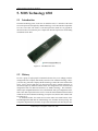
5. MOS Technology 6502
5.1 Introduction
The MOS Technology 6502, from now on called the 6502, is a member of the 6500
series microprocessors designed by MOS Technology. It was introduced in September
1975 at a cost of $25. The 6502 is a 8-bit microprocessor which was very popular at
the time because of its attractive price compared to other microprocessors from leading
manufacturers like Intel.
Figure 5.1: The MOS 6502 CPU
5.2 History
In 1974 a group of eight people left Motorola because they were unhappy with the
management at the company. Instead they started to work at MOS Technology. Only a
year after they joined the company, MOS Technology released the 6501 and the 6502
CPUs. Due to the fact that these two microprocessors had a similar architecture to
the 6800 designed by Motorola and that those who designed the 6501 and 6502 had
designed the 6800 too, Motorola decided to sue MOS Technology. The 6502 had a
different pin configuration than the 6501, which had the same pin configuration as the
6800. This made it possible for the 6501 to fit into the 6800 motherboard and resulted
in that the lawsuit forced MOS Technology to stop the 6501, but the 6502 could be still
be produced [3].
As mentioned earlier, the 6502s success on the market was much because of the
breakthroughs MOS had made in manufacturing costs, and thus end-user pricing. The
competitor chip from Intel, the 8080, was priced at about $150 at the time. By the time
Student Papers in Computer Architecture, 2006
22
CHAPTER 5. MOS TECHNOLOGY 6502
Intel and other manufacturers dropped their prices to better match the 6502, the new
chip had already gained a considerable market share and was already selling by the
hundreds [2].
5.3 Implementations
The 6502, in its many forms, has been used in many systems and is still widely used.
The most familiar implementations where you can find the 6502 is in early computers like the Apple I, the Commodore 64, the Atari 400 and probably one of the most
world wide known system, by Nintendo, the NES1 . The processor was also running
Commodores first personal computer, the Commodore PET (also known as the first
full-featured personal computer).
Figure 5.2: The Apple I, in wood casing
5.4 Technical data
•
•
•
•
•
•
8-bit bidirectional data bus
16-bit address bus (64 KB of addressable memory)
Operating frequencies ranging from 1 MHz to 4 MHz
56 instructions
13 addressing modes
Programmable stack pointer
5.4.1 Registers
The 6502 contains one 8-bit accumulator (A), two 8-bit index registers (X,Y), one 8-bit
stack pointer (S), one 8-bit processor status register and one 16-bit program counter.
The small number of registers would, however, not prove to be a limitation thanks to
the indirect addressing modes (mode 10 on the next page) which supplied an extra 1282
registers to use [1].
1 Nintendo
2 The
Entertainment System
16-bit pointers are stored on the zero page, which results in 128 usable indirect registers.
September 29, 2006
Andersson and Ågren (editors)
T OMAS S JÖDIN AND J OHAN J ONSSON
23
5.4.2 Addressing modes
The 6502 has eleven different addressing modes. However, since both the X and Y
register can be used for indexed zero page addressing and index absolute addressing
these are sometimes considered to be four different modes3 , and thus resulting in a total
of thirteen different addressing modes.
1. Accumulator addressing uses one byte instructions, which means the operation
will be performed on the accumulator.
2. Immediate addressing uses the second byte of the instruction as the operand for
the operation.
3. Absolute addressing uses the two subsequent bytes of the instruction for the
eight low order bits and high order bits of the address respectively. This makes
all of the 64K bytes of memory addressable.
4. Zero page addressing is a simpler variant of Absolute addressing, using only
the first byte after the instruction and assuming zero for the high order bits. By
saving the cycle it takes to fetch the second byte, this allows faster execution
and shorter code and can, if used carefully, result in a significant performance
increase.
5. Indexed zero page addressing adds the first byte after the instruction and one
of the index registers to address a location in page zero4 . Only the zero page can
be addressed since no carry is added to the high order bits.
6. Index absolute addressing adds the X and Y registers to the 16-bit address
supplied in the two subsequent bytes of the instruction. This addressing mode
makes it possible to use the index registers as a counter and the supplied address
as a base address to any location for modification of multiple fields.
7. Implied addressing is when the source and destination is implicitly specified
in the operation code of the instruction. These instructions need no further
operands. Instructions like CLV (Clear Overflow flag) and RTS (Return From
Subroutine) are implicit.
8. Relative addressing is used for conditional branch (jump) instructions. The byte
subsequent to the instruction becomes the offset which is added to the lower eight
bits of the program counter.
9. Indexed indirect addressing adds the supplied operand with the contents of the
X register. The contents of the resulting address at page zero (carry is discarded)
becomes the low order eight bits of the resulting address. The next location on
page zero becomes the high order eight bits of the resulting address.
10. Indirect indexed addressing adds the supplied zero page address with the contents of the Y register resulting in the eight low order bits of the target address.
The carry is then added to the address on the location next on page zero to produce the eight high order bits of the target.
11. Absolute indirect addressing uses a 16-bit address operand which points to
another 16-bit address, which is the real target of the instruction.
3 These
modes are often referred to as Zero Page.X, Zero Page.Y, Absolute.X and Absolute.Y, where the X
or Y specifies the register used.
4 “Page zero” or “the zero page” are the first 256 memory locations (the amount addressable by an 8-bit
pointer)
Student Papers in Computer Architecture, 2006
24
CHAPTER 5. MOS TECHNOLOGY 6502
5.4.3 Pipelining
By fetching the next instruction during the execution of another, the 6502 accomplishes
a form of pipelining and thus manages to save one cycle per instruction. This can
only be done if no data is stored in the memory when executing the last cycle, and
the processor can then get the opcode for the next instruction at the same time as it
performs the operation given by the instruction.
5.4.4 Instructions
The 6502 is using a multi-cycle approach when executing instructions, which mean
that an instruction is executed during several clock cycles. The 6502 has no MUL or DIV
instructions and neither does it support floating point operations [1].
5.5 Performance
When the 6502 was introduced in 1975 it ran at a 1 MHz clock frequency, which was
the same as the Motorola 6800, but was about four times faster (thanks to pipelining) [2]. This was also the case when comparing the 6502 to Intel processors of the
time, which could run at a clock frequency four times higher to perform at the same
level as a 6502 [4].
5.6 References
[1] B UTTERFIELD , J. The new 6500 chips. Compute! (Feb. 1983), 196. Reproduced
at http://www.commodore.ca/history/company/6502/6500cpus.htm.
[2] M ATTHEWS , I. The Rise of MOS Technology & The 6502. Web page, June 26,
2006. http://www.commodore.ca/history/company/mos/mos_technology.htm.
[3] S LATER , M. The 6502’s Long Path to The Western Design Center. Microprocessor
Report (July 11, 1994). Published by Micro Design Resources, reproduced at
http://apple2history.org/museum/articles/microreport/microreport.html.
[4] W EYHRICH ,
S.
Apple II history.
Web page,
May 31,
2006.
http://apple2history.org/history/ah12.html.
September 29, 2006
Andersson and Ågren (editors)
DANIEL E KSTRÖM
25
6. Motorola 68000
6.1 Introduction
6.1.1 History
The Motorola 68000 grew out of the MACSS (Motorola Advanced Computer System
on Silicon) project, begun in 1976. It is also known as simply 68k. One of the early
goals was to design a new architecture that wouldn’t suffer from backward compatibility problems. This meant that users of the new chip would have to learn everything
from scratch, which was a gamble. The MACSS team was heavily influenced by the
mainframe processor design, like the PDP-11 and VAX. The idea behind developing
the 68000 processor was that developers around the world that were familiar with these
older systems would be comfortable programming this new microprocessor.
The first versions of the 68000 processor was first released in 1979, which was
during the time when the competition was advancing from 8-bit processors to 16-bit
processors. The 68000 had a more complete design than the competition, like the Intel
80386, and had more than twice the amount of transistor cells. The 68000 was actually
named after the number of transistor cells, even though it in reality had around 70,000
cells [6].
6.1.2 Predecessors
Some might say that the name 68000 refers to that it’s an upgrade from the Motorola
6800 CPU. Although there isn’t much resemblance between the two architectures, we
could still call the 6800 a predecessor to the 68000 [9].
6.2 Overview of the processor
6.2.1 Registers
The CPU has eight general purpose data registers (D0-D7) and another eight address
registers (A0-A7), with the last address register known as the standard stack pointer,
called A7 or SP. The number of registers was big enough to make most calculations fast,
but yet small enough to allow it to answer quickly to interrupts. Integer representation
in the 68000 family was big-endian [8].
6.2.2 Instructions
The different instructions in the 68000 were divided into operations and address modes,
where almost all addresses were available for every instruction. At the bit level, the
programmer could clearly see that these instructions easily could become any of these
different op-codes. Some programmers liked this while some didn’t.
Student Papers in Computer Architecture, 2006
26
CHAPTER 6. MOTOROLA 68000
The minimal instruction size was 16 bits, which was huge back in those days. Each
instruction accepts either 0, 1 or 2 operands, and most instructions alter the condition
codes [1].
6.2.3 Implementations
It was originally designed for use in household products (according to Motorola), and
was used for the design of computers from Amiga, Apple Macintosh, Atari and Sun.
It was also used as main CPU in the Sega MegaDrive, NeoGeo and several Arcade
machines, while the Sega Saturn used it as a sound chip.
Back in the early 1980s, the Motorola 68000 were used in high-priced systems
including multiuser microsystems like the WICAT 150, Tandy TRS-80 Model 16, Sun
Microsystems Sun-1 among others. It was also used in graphics terminals like Digital
Equipment Corporation’s VAXstation 100 and Silicon Graphics IRIS 1000 and 1200.
The 68000 and its derivatives continued in the UNIX market for many years and was
an excellent architecture for running C code.
It wasn’t until the later 1980s that the 68000 was used in personal computers and
home computers, like the Apple Lisa and the Macintosh, followed by the Atari ST and
the Commodore Amiga [5].
Figure 6.1: Overview of the Motorola 68000
6.3 Memory hierarchy
6.3.1 Virtual memory
The 68000 didn’t have any virtual memory since it couldn’t restart interrupted instructions. In 1982 this was added to the 68010 processor along with a special loop mode
that allowed small decrement-and-branch loops to be executed from the instruction
fetch buffer [2].
September 29, 2006
Andersson and Ågren (editors)
DANIEL E KSTRÖM
27
6.4 Execution
6.4.1 Interrupts
The 68000 recognized seven interrupt levels. The higher the number, the higher priority. This meant that a higher number interrupt could always step in before a lower
number interrupt. Hardware interrupts are signalled to the CPU using three inputs that
encode the highest pending interrupt priority. For systems requiring more than three
hardware interrupts, a separate interrupt controller was required to encode them [8].
6.4.2 Performance
As mentioned before the instructions accept 0, 1 and 2 operands. One consequence
of the 2-operand format is that the instruction might have to use the same part of the
hardware several times during a single instruction. For example, the instruction
add \#7, D1
reads the contents of register D1, adds 7 to that value and puts the result back in D1.
The command then sets the appropriate condition codes in the status register. Such
heavy dependencies on a small number of resources means that every instruction has to
complete before the next can begin, which effectively prevents the use of pipelining [1].
Some performance numbers [4]:
• Operating frequency: 8 - 20 MHz
• CPU performance: 2 MIPS max at 20 MHz
• Bus interface: 16-bit, 8-bit or 16-bit
• L1 cache instructional: 0 KB
• L1 cache data: 0 KB
6.4.3 Pipelining
As previously mentioned, the 68000 couldn’t really handle any pipelining. As a side
note, the Motorola 68060 was a fully pipelined superscalar processor which allows
simultaneous execution of 2 integer instructions (or one integer and one floating point
instruction) and one branch during each clock cycle [7].
6.4.4 Exceptions
Exception processing results from interrupts, a bus, trap exceptions or address error
or a reset. This action simplifies development by detecting errors and keeps “runaway” conditions from happening. The exception vector table is often made of 255 32bit vectors using 1024 KB of memory starting at location zero. The CPU loads the
appropriate vector, containing the 32-bit address of the routine to service the exception,
Student Papers in Computer Architecture, 2006
28
CHAPTER 6. MOTOROLA 68000
from this table at the occurrence of an exception such as reset, bus or address error,
word access to odd memory location, trap and others.
This table is usually constructed by the operating system in RAM during the start
up period. There is a total of 192 reserved user interrupts. The initial SSP (Supervisor
Stack Pointer) and initial PC takes up memory location $0 and $4 which usually maps
out to ROM. The only way for the CPU to switch from user mode to supervisor mode
is via exception processing.
Most programs are meant to execute in user mode. The supervisor mode is often used for the operating system and software accessing system resources. At reset,
the processor is in the supervisor mode and a system can operate continuously in this
mode [3].
6.5 References
[1] A PPLE C OMPUTER , I NC. Two representative CISC designs. Web page, Mar. 12,
1995. http://physinfo.ulb.ac.be/divers_html/PowerPC_Programming_Info/intro_to_risc/irt4_cisc3.html.
[2] BAYKO , J.
The great CPU list, section three.
Web page, Mar. 30, 2003.
http://www.sasktelwebsite.net/jbayko/cpu3.html.
[3] B OYS ,
R.
M68K
FAQ
9.
Web
page,
Oct.
19,
1994.
http://archive.comlab.ox.ac.uk/cards/m68kfaq.html.
[4] F REESCALE S EMICONDUCTOR , I NC.
MC68000 product summary page.
Web page, Sept. 27, 2006.
http://www.freescale.com/webapp/sps/site/prod_summary.jsp?code=MC68000, date visited given.
[5] H EXA F IND.
The Motorola 68000.
Web page,
Sept. 27,
2006.
http://www.hexafind.com/encyclopedia/M68000, date visited given.
[6]
T S CHOLARS . COM.
The Motorola 68000.
Web page, Feb. 23, 2006.
http://www.tscholars.com/encyclopedia/Motorola_68000.
[7] W ESLEY, T.
Pipelining:
Motorola 68060.
Web page, Sept. 7, 2002.
http://www.wideopenwest.com/~awesley5155/p_5_1.html.
[8] W IKIPEDIA.
The Motorola 68000.
Web page,
Sept. 27,
2006.
http://en.wikipedia.org/wiki/Motorola_68000, date visited given.
[9] W IKIPEDIA.
Talk:
Motorola 68000.
Web board, Sept. 20, 2006.
http://en.wikipedia.org/wiki/Talk:Motorola_68000#Motorola_6800.
September 29, 2006
Andersson and Ågren (editors)
O MAS JAKOBSSON AND M ARTIN N ILSSON
29
7. PIC 16F84
7.1 Introduction
The PIC16F84 is a microcontroller developed and produced by Microchip Technology
Inc [2]. It belongs to the the PIC16CXX family of CMOS microcontrollers and is used
for applications like remote sensors, security devices and smart cards [4].
The PIC16F84 is a successor of PIC16C84, which was released in March 1993 [2].
Important improvements from PIC16C84 include a Flash program memory instead
of EEPROM and an increased amount of RAM from 36 to 68 bytes [4, 3]. Other
variations of the PIC16CXX family include PIC16F83, PIC16CR83 and PIC16CR84.
The PIC16CXX family is developed from the PIC15C5X family [4].
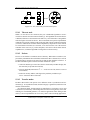
7.2 Overview
The PIC18F8X devices are all RISC-based microcontrollers with a set of advanced core
features, such as its memory architecture, multiple interrupts and its high performance.
Figure 7.1 on the following page shows a simplified overview of the PIC16F8X.
7.2.1 Specifications
The PIC16F84 features an 8-bit data bus and ALU, but has a 14-bit program bus, which
serves the purpose of allowing a 5-bit direct addressing towards the file register as seen
in figure 7.1 on the next page.
In addition to this, the PIC16F84 also has an 8-level deep 13-bit callstack, where
program calls can be stacked. The stack is connected to the program memory through
a 13-bit wide bus.
The PIC16F84 has 15 8-bit SPRs (special purpose registers) in addition to the 68
8-bit GPRs (general purpose registers) [4]. These special registers are used for more
specialized tasks, such as accessing the EEPROM. The GPRs and SPRs are both part
of a common structure that is divided into two banks, in order to allow a larger number
of registers to be accessed. Each bank contains 12 positions reserved for SPRs and the
rest are GPRs. Most of the SPRs in the two banks are mapped to the same location and
all of the GPRs in the second bank are mapped to the first.
Access to the different banks is done by manipulating bits in a status register that
also contains different status information from the ALU.
7.2.2 Implementations
The low cost, low power and low space requirements of the PIC16F84 make it suitable
for smartcard applications such as access control to buildings since the microcontroller
can be embedded in a wallet size card.
Other applications may be for example controlling motor speed or displaying sensor information on an LCD display.
Student Papers in Computer Architecture, 2006
30
CHAPTER 7. PIC 16F84
Figure 7.1: PIC16F8X Block Diagram [4]
7.3 Memory architecture
The PIC16CXX and PIC16FXX use a Harvard architecture, where data and program
memory are held separate, which also means that they have separate busses for accessing these types of memory.
This design allows for instructions to be sized differently than if the device has
to consider how data memory is addressed, which in turn increases the performance
of execution since the the different kinds of memory can be addressed in the same
cycle. Figure 7.2 on the facing page shows the layout of the program memory and
the callstack. As seen, the implemented program memory is only 1 K×14 bits and
accessing memory above this memory space will cause the address to wrap around.
In addition to program memory, there is also 64×8 bits of EEPROM Data Memory (Electrically Erasable Programmable Read-Only Memory). EEPROM retains data
even if power is lost, which makes it ideal for storing more or less permanent information.
Reading and writing to the EEPROM memory is however a bit tricky, since access to it is done through four special registers: EECON1, EECON2, EEDATA and
EEADR. To read a single byte, the RD bit (bit 0) IN EECON1 is set, followed by a
write to EEADR, where the address to the memory that is to be read is placed and
finally reading can occur from the EEDATA register, which holds the requested byte.
Writing to EEPROM memory follows a similar pattern.
September 29, 2006
Andersson and Ågren (editors)
O MAS JAKOBSSON AND M ARTIN N ILSSON
31
Figure 7.2: PIC16F84/PICCR84 Program memory [4]
7.4 Execution and Performance
The PIC16F84 has an external clock which controls the speed of the CPU. Clock cycles
from the clock input are divided into groups of four. This group is called an “Instruction
Cycle”, and the individual clock cycles are called Q cycles, where Q1 is the first clock
cycle in an instruction cycle, Q2 the second and so on up to Q4 [4, page 10]. Every
instruction needs two instruction cycles to complete, the first to fetch the instruction
from program memory and the second to decode and execute the instruction. Since the
maximum speed of the clock is 10 MHz, the minimum cycle time of a Q cycle is 100
ns and thus one instruction cycle is 400 ns [4, page 1].
In the beginning of the fetch cycle, in Q1, the program counter is incremented and
the next instruction is moved from the program memory to the instruction register. In
Q1 of the next instruction cycle the instruction is decoded and in Q2 data is read from
memory, if necessary. When everything needed for the execution of the instruction has
been acquired the instruction is executed during Q3 and the result written to memory
in Q4 [4, page 10].
Because of the Harvard memory architecture the program memory and data memory have separate busses, which makes it possible to read from both memories simultaneously [1]. This gives an opportunity for effective pipelining by reading the next instruction while executing the current one, resulting in that instructions being effectively
executed in one clock cycle. As noted above one instruction cycle is 400 ns, which
gives that 2.5 million instructions can be executed per second. A few instructions,
however, cannot be pipelined in this manner. These instructions are those that cause
the program counter to change, e.g. branching. This is because the fetch instruction is
Student Papers in Computer Architecture, 2006
32
CHAPTER 7. PIC 16F84
flushed from the pipeline while the new instruction is being fetched [4, page 10].
The PIC16F84 can also handle four types of interrupts [4, page 48]. All four have
set bits in the interrupt control register (INTCON) which decide if an interrupt event
should trigger an interrupt or not. There is also a global bit to set if interrupts should
be disabled completely. If listening for an interrupt is enabled and the interrupt occurs
the global bit is cleared to disable any further interrupts. Then the value of the program
counter is stored in the callstack and the counter is set to a predefined value, 0004h,
where the interrupt handler routine is located. The four interrupts available in the
PIC16F84 are
• External interrupt RB0/INT — The RB0/INT pin can be set to trigger an interrupt
on either the rising or falling edge.
• TMR0 overflow interrupt — TMR0 is an 8-bit clock counter which eventually
will overflow. When that occurs this interrupt will be triggered.
• PORTB change interrupt — Just as the RB0/INT pin, the PORTB pins can be set
to trigger interrupts on input change.
• Data EEPROM write complete interrupt — A completed write to the EEPROM
will trigger this interrupt.
7.5 Special features
The PIC16F84 includes some special features to set it apart from other microcontrollers. One of these features is the watchdog timer. This timer is a free running
on-chip timer independent of the clock on the CLKIN pin. Another feature is the sleep
mode. Sleep mode is used to conserve energy while the controller is unused. While
sleeping the watchdog timer can be used as an alarm to wake the device up after a
specified period of time [4].
7.6 References
[1] I OVINE , J. PIC Microcontroller Project Book. McGraw-Hill Professional, 2000.
Also available at http://site.ebrary.com/lib/umeaub/Doc?id=5004057&ppg=5.
[2] M ICROCHIP TECHNOLOGY INC . MICROCHIP UNVEILS PIC 16C84, A REPROGRAMMABLE EEPROM-BASED 8-BIT MICROCONTROLLER, AND
PICMASTER-16C, A NEW SUPPORTING DEVELOPMENT TOOL. Web
page, Sept. 20 1993.
Available at http://www.microchip.com/stellent/idcplg?IdcService=SS_GET_PAGE&nodeId=2018&mcparam=en013082.
[3] M ICROCHIP
TECHNOLOGY
EEPROM
Microcontroller,
8-bit
CMOS
available
at
http://ww1.microchip.com/downloads/en/DeviceDoc/30445c.pdf.
[4] M ICROCHIP TECHNOLOGY
8-bit
Microcontrollers,
INC .
1997/1999.
PIC16C84
Also
PIC16F8X 18-pin Flash/EEPROM
1998/2002.
Also
available
at
http://ww1.microchip.com/downloads/en/DeviceDoc/30430c.pdf.
September 29, 2006
INC .
Andersson and Ågren (editors)
K JELL W INBLAD AND A NDERS H ANSSON
33
8. PowerPC 750
8.1 Introduction
The PowerPC 750 is a 32-bit implementation of the PowerPC Reduced Instruction
Set Computer architecture (RISC). PowerPC 750 is a member of the PowerPC family.
The PowerPC line started with the PowerPC 601 in March 14, 1994. The 601 had an
initial speed of 66 MHz. It provided a bridge between the PowerPC and the POWER
architecture. POWER stands for Performance Optimisation With Enhanced RISC and
is IBM’s RISC architecture developed for servers. Before the PowerPC 601 Apple
used Motorola’s 68000 processor for it’s desktop computers. Apple needed a CPU that
was backward compatible with the 68000, IBM wanted to reach a wider range with the
POWER architecture and Motorola needed a high-end RISC processor to compete in
the RISC market. The alliance AIM (Apple, IBM, Motorola) was born and soon after
that the PowerPC architecture derived from the POWER architecture. The PowerPC
750 version distributed by Motorola is called MPC750 and the version distributed by
IBM is called PPC750 [6].
The PowerPC 750 was introduced on the market at the 10th of November 1997. At
that time it had a clockspeed of 233-266 MHz. It first appeared, with the name G3, in
Apple’s Power Macintosh G3/233. G3 is the predecessor of PowerPC 7400, by Apple
called G4 [7].
8.2 Overview of the processor
The Power PC 750 has a RISC architecture. The processor has 32 GPRs (General
Purpose Register), 32 FPRs (Floating Point Register), some SPRs (Special Purpose
Register) and miscellaneous registers. The GPRs are used for all integer arithmetics.
Most of the arithmetics instructions take three registers as parameters. One to save
the result and two for operands. The FPRs are 64bits and can be used too hold both
single (32 bits) and double (64 bits) floating point numbers. The floating point system
is IEEE 754-1985-compliant but a special non-IEEE mode can be used for special time
critical operation [3].
8.2.1 Registers
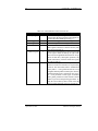
The processor can operate in two modes: user mode and supervisor mode. The registers
that can be used in user mode is a subset of those that can be used in supervisor mode.
See table 8.1 for an example of registers that’s in user mode and supervisor mode.
The purpose of having modes with different access levels is to make it more easy
and effective to implement a secure operating system. The operating system can run
in supervisor mode and the user program can run in user mode which makes it much
more easy to control what user programs can do [3].
Student Papers in Computer Architecture, 2006
34
CHAPTER 8. POWERPC 750
Register name
CR
Level
User
CTR
User
LR
User
FPRs
User
TB
U:R S:RW
MSR
Supervisor
SRs
Supervisor
SPRs
Supervisor
Purpose
(Condition Register) Is used in comparison instructions and branching etc.
(Count Register) Is used by branch-and-count instruction.
(Link Register) Link address that is used to hold
the branch target address and the return address in
branch and link instruction.
(Floating Point Register) 32 registers that are used
in floating-point arithmetics.
(Time Base Register) Read-only register for user
that contains the system time. Can be written to,
in supervisor mode.
(Machine State Register) When an exception occurs the exception number is saved to the register
and when the exception handling is finished, it’s
cleared.
(Segment Register) Is used to access memory segments. The memory is divided into 16 segments
where each can contain 256 MB of data. The first
register is used to access the first segment and so
on.
(Special Purpose Register) Operating system specific registers like registers that hold instruction
address for restoring after an exception etc.
Table 8.1: The table shows some important registers and if they are available in user
mode
8.2.2 Implementations
The most famous computer that uses the PowerPC 750 is probably the first versions of
iMac which was built by Apple. But it had been used in many other types of computers [5].
RAD750 is a PowerPC 750 implementation for use in spaceship and other systems that are exposed to radiation. It’s developed by the company BAE Systems. The
processor was first sold in 2001 [1].
Many operating systems have been ported to the PowerPC 750 architectures. Some
examples are Mac OS, Linux, Solaris, FreeBSD and MorphOS [2].
September 29, 2006
Andersson and Ågren (editors)
K JELL W INBLAD AND A NDERS H ANSSON
35
8.3 Memory hierarchy
8.3.1 Memory management units (MMU)
The PowerPC 750 has two MMUs, one for the instruction cache and one for the data
cache. The main task of the MMUs is to translate effective addresses into physical
addresses used in the memory access. The effective address is calculated by the loadstore unit (LSU). For instructions and data the MMUs support up to 4 Petabytes of
virtual memory and 4 Gigabytes of physical memory. The MMUs also control access
privileges for these spaces [3].
8.3.2 Instruction and data caches
The PowerPC 750 has two 32 KB, on-chip, eight-way set associative caches. One for
instructions and one for data. This means that we have 128 sets; each set consists of
eight blocks and each block has place for eight words in each cache. The eight words
in one block are adjacent words from the memory that are loaded from an eight-word
boundary. The caches are nonblocking, write-back caches. The caches are physically
indexed [3].
The data cache can provide double-word access to the load-store unit within one
cycle and the instruction cache can provide up to four instructions to the instruction
queue within one cycle [3].
The PowerPC 750 also has a 64-entry branch target instruction cache (BTIC). The
cache has 16 sets and are four-way set associative. The BTIC cache contains instructions that have been encountered in a loop sequence [3].
8.3.3 L2 cache
The L2 cache is implemented with an on-chip, two-way set-associative tag memory,
and an external, synchronous SRAM for data storage. To access the external SRAM
there is a dedicated L2 cache port that supports a single bank of up to 1 MB of synchronous SRAM. Normally the L2 cache operates in write-back mode and it also supports system cache coherency through snooping. The L2 cache receives memory requests from the two L1 caches (data and instruction cache). The memory request from
the L1 caches often are results of instruction misses, data load and store misses, write
through operations or cache management instructions. The request from the L1 caches
are looked up in the tags of the L2 cache, if the requests miss they are forwarded to the
bus interface [3].
The L2 cache can handle several request at the same time. The L1 instruction cache
can request one instruction while the L1 data cache at the same time can request one
load and two store operations. The L2 cache supports snoop requests from the bus.
If there are several pending requests to the L2 cache, the one with highest priority
goes first. Snoop requests have the highest priority, then comes load and store instructions from the L1 data cache and then instruction fetch request from the L1 instruction
cache [3].
Student Papers in Computer Architecture, 2006
36
CHAPTER 8. POWERPC 750
8.4 Execution
The PowerPC 750 processor uses a more advanced and performance optimised execution if you compare it to its predecessor. The most important units and parts of the
execution is described in the sections below.
8.4.1 The Instruction Queue
Instructions are loaded into an instruction queue (IQ) from the instruction cache before
execution. The IQ can hold a maximum of six instructions. A maximum of four
instructions can be loaded per clock-cycle by the instruction fetcher. The instruction
fetcher tries to load as many instruction as there are empty places in the queue [3].
8.4.2 Branch Processing Unit
The PowerPC 750 processor has a Branch Processing Unit (BPU) that is used for optimising branching. The BPU calculates branch addresses on fetched branches if possible. It’s important for the performance to calculate branches early, because then new
instructions can be fetched from the instruction cache. The PowerPC 750 can use
both dynamic and static branch prediction if it isn’t possible to calculate a branch directly. When a prediction is done the fetcher can fetch instructions from the predicted
branch but instructions could not be completed before the BPU has determined that
the branch was correctly predicted. When the branch has been determined the results
from predicted branch is either saved to registers or deleted. The BPU can predict two
branches but instructions from the second branch could not be executed before the first
is ready [3].
The dynamic branch prediction uses a 512-entries branch history table to predict
branches. Each element in the table contains two bits that indicate the level of prediction. The number is set depending on previous branches. There also exists a table
with 64 entries (BTIC) that contains the first instruction in branches that are recently
taken. The table makes it faster to start execution of new branches. An instruction can
be fetched one clock cycle faster from BTIC than from the instruction cache [3].
8.4.3 Dispatch Unit, Completion Queue and Pipelining
The dispatch unit can take maximum two instructions from the instruction queue per
clock cycle. The instructions are passed to its corresponding execution unit. There are
two integer units (IUs), one floating point unit (FPU), one load/store unit (LSU) and
one system register unit (SRU) that can handle instructions. The dispatch unit checks
for dependences in source and destination registers. Thus the processor is a superscalar
processor [3].
Like all modern processors the Power PC 750 uses pipelining. To make it easy
to recover when branches have been wrongly predicted and when exception occurs,
the processor has a Completion Unit (CU). The CU has a Completion Queue (CQ)
with six entries. An entry is created in the instruction queue when the instruction is
dispatched. If the CU is full the dispatch unit has to wait until there are empty places.
September 29, 2006
Andersson and Ågren (editors)
K JELL W INBLAD AND A NDERS H ANSSON
37
When instructions in the queue are completed their results are written to registers by
the completion unit [3].
8.4.4 Execution Units
The PowerPC has several independent Execution Units (EU) that perform the execution
of instructions. See table 8.2 for a short description of each.
Unit Name
Integer Unit 1 (IU1)
Integer Unit 2 (IU2)
Floating-Point Unit (FPU)
Load/Store Unit (LSU)
System Register Unit (SRU)
Purpose
Performs integer arithmetics instruction like division,
addition and logic operations etc.
The same as IU1, but can’t perform division and multiplication.
Is used for floating-point number instructions. It is
pipelined in such way that one single and one doubleprecision instruction can be passed to it per clock cycle. The latency for instructions is three cycles.
Used to store and load data from the cache and memory system. Data that is returned from the cache and
memory system is saved in a register until the Competion Unit commits it to its destination.
The SRU performs system level instruction and instructions to move data from and to Special Purpose
Registers.
Table 8.2: The table gives a short description of every execution unit.
8.5 Performance
The information below is taken from the MPC750 fact sheet [4].
CPU Speeds Internal
Bus Interface
Instructions per Clock
L1 Cache
L2 Cache
Die Size
SPECfp95 (estimated)
SPECint95 (estimated)
Other Performance
MPC750 200-266 MHz
200, 233 and 266 MHz
64-bit
3 (2 + Branch)
32 KB instruction
32 KB data
256, 512 KB 1 MB
67 mm2
7.4 @ 266 MHz
12.0 @ 266 MHz
488 MIPS @ 266 MHz
MPC750 300-400 MHz
300, 333, 366 and 400 MHz
64-bit
3 (2 + Branch)
32 KB instruction
32 KB data
256, 512 KB 1 MB
67 mm2
12.2 @ 400 MHz
18.8 @ 400 MHz
733 MIPS @ 400 MHz
Table 8.3: Performance specifikation for MPC750.
Student Papers in Computer Architecture, 2006
38
CHAPTER 8. POWERPC 750
8.6 References
[1] BAE S YSTEMS.
RAD750TM Space Computers, 2004.
Also available at
http://www.eis.na.baesystems.com/sse/rad750.htm.
[2] G ENESI USA, I NC .
PegasosPPC software.
Web page, Sept. 20, 2006.
http://www.pegasosppc.com/software.php, date visited given.
[3] M OTOROLA I NC ., AND IBM C ORP. PowerPC 750 RISC Microprocessor Technical Summary, Aug. 1997. Also available at http://www-3.ibm.com/chips/techlib/techlib.nsf/techdocs/852569B20050FF778525699300470399/.
[4] M OTOROLA I NC . FACT SHEET: MPC750 AND MPC740 MICROPROCESSORS, 2002. Also available at http://www.freescale.com/files/32bit/doc/fact_sheet/MPC750FACT.pdf.
[5] S ANFORD , G.
www.apple-history.com.
Web page, Sept. 20, 2006.
http://www.apple-history.com/?model=imac, date visited given.
[6] S TOKES , J. PowerPC on Apple: An Architectural History, Part I. Ars Technica (Aug. 3, 2004). Available at http://arstechnica.com/articles/paedia/cpu/ppc-1.ars/1.
[7] S TOKES , J. PowerPC on Apple: An Architectural History, Part II. Ars Technica
(Oct. 18, 2004). Available at http://arstechnica.com/articles/paedia/cpu/ppc-2.ars/1.
September 29, 2006
Andersson and Ågren (editors)
N ICLAS H ELLBERG AND J OHAN S VEDBERG
39
9. PowerPC G5
9.1 Introduction
The PowerPC G5 is a processor used in Apple’s desktop and server computers. It was
introduced in June 2003 as the product of a partnership between Apple and IBM [1].
The manufacturer, IBM, called it PowerPC 970. It is based on IBM’s POWER4 processor and is built with 64-bit technology [1]. The term G5 in this context stands for
the fifth generation of PowerPC processors and the predecessor for it was the G4 [5].
Further development was made on the PowerPC 970: 970FX and 970MP.
The G5 series consist of the following models [4]:
• 970 (2003), 130 nm, 512 KB L2 cache, 1.4 - 2 GHz
• 970FX (2004), 90 nm, 512 KB L2 cache, 1.8 - 2.7 GHz
• 970MP (2005), 90 nm, dual core, 1 MB L2 cache/core, 1.6 - 2.5 GHz
9.2 Overview of the processor
IBM uses a 90-nanometer process with more than 58 million transistors and eight layers of copper interconnects. The PowerPC G5 uses copper interconnects to transmit
electrical signals faster and more reliably than aluminum can. It has three register files,
each holding 32 architected values and 48 rename registers. One file with 64-bit registers for integer calculations, one file with 64-bit registers for floating-point calculations
and one vector register file to contain 128-bit registers for vector calculations [1]. It
has a Double Data Rate (DDR) frontside bus that has two 32-bit point-to-point links
(64 bits total): One link travels into the processor and another travels from the processor, which means no wait time while the processor and the system controller negotiate
which will use the bus or while the bus switches direction. On a 2 GHz PowerPC G5,
the frontside bus operates at 1GHz for a total theoretical bandwidth of up to 8 GB/s [1].
The PowerPC G5 processor is implemented in the consumer version iMac G5 and
in the professional models PowerMac G5 and Xserve G5 [6].
It is a supercalar execution core with 12 execution units working in parallel [3]. In
Figure 9.1 on the next page there is an overview of the parts in the processor.
Student Papers in Computer Architecture, 2006
40
CHAPTER 9. POWERPC G5
Figure 9.1: PowerPC G5
9.3 Memory hierarchy
The memory in the G5 consists of 42-bit physical and 64-bit virtual address ranges.
This means that theoretically there is support for 4 terabytes of RAM and 18 million
terabytes of virtual memory [2].
9.3.1 Cache
Cache memory is divided into two levels, L1 and L2. L1 is split up in two parts, a 64
KB direct-mapped instruction cache (I-cache) and a 32 KB 2-way associtive data cache
(D-cache) [3]. The L2 cache is 512 KB and can receive data at rates up to 64 GB/s, see
Table 9.1 on the facing page [1].
The G5 can predict the need for data and instructions and prefetch them into the
L1 and L2 caches before they are demanded by the processor, which makes optimal
utilization of each clock cycle. At work, instructions are fetched from the L2 cache
into the I-cache. Simultaneously the D-cache can fetch up to eight active data streams
in parallel with 32 KB write-through [1].
September 29, 2006
Andersson and Ågren (editors)
N ICLAS H ELLBERG AND J OHAN S VEDBERG
41
Table 9.1: Cache memory layout [3]
L1 cache
L2 cache
I-cache
D-cache
64 KB
32 KB
512 KB
direct-mapped 2-way assoc. 8-way assoc.
9.4 Execution
Up to eight instructions per clock cycle can be retrieved from the L1 instruction cache
for decoding. Decoding splits each instruction into smaller sub-operations which gives
the processor freedom to make optimizations like parallel code execution. The G5
dispatches instructions into groups of five to issue queues in the execution core, where
they are processed out-of-order as individual instructions. By managing instructions in
groups the G5 is able work more efficiently, peaking at 215 in-flight instructions [1].
The G5 has a superscalar processor which concists of 12 functional units that execute different types of instructions simultaneously. See Table 9.2 on the next page for
descriptions of the different parts.
After execution the instructions are grouped back into their earlier groups.
9.5 References
[1] A PPLE C OMPUTER , I NC . PowerPC G5. White Paper, Jan. 2004. Available at
http://images.apple.com/server/pdfs/L301298A_PowerPCG5_WP.pdf.
[2] G REVSTAD , E. The New Apple Core: IBM’s PowerPC 970/G5. Web page, July 9,
2003. http://www.cpuplanet.com/features/article.php/2233261.
[3] S TOKES , J. H.
Inside the IBM PowerPC 970.
Web page, Oct. 28, 2002.
http://arstechnica.com/cpu/02q2/ppc970/ppc970-1.html.
[4] W IKIPEDIA.
PowerPC.
Web
page,
Sept.
20,
2006.
http://en.wikipedia.org/wiki/PowerPC, date visited given.
[5] W IKIPEDIA.
PowerPC
970.
Web
page,
Sept.
20,
2006.
Sept. 20,
2006.
http://en.wikipedia.org/wiki/PowerPC_970, date visited given.
[6] W IKIPEDIA.
PowerPC Mac G5.
Web page,
http://en.wikipedia.org/wiki/Power_Mac_G5, date visited given.
Student Papers in Computer Architecture, 2006
42
CHAPTER 9. POWERPC G5
Table 9.2: Functional units in the execution core.
Unit
# of units Description
Velocity Engine
4
A 128-bit vector processing unit used to simultaneously apply the same instruction to multiple sets
of data, also called SIMD processing [1].
Floating-point
2
Performs floating-point calculations [1].
Integer
2
Performs integer calculations [1].
Load/Store
1
Loads data from the L1 cache into the functional
units registers and stores it back to memory after
it has been processed [1].
Condition register
1
Instructions can optionally save their results in this
32-bit register which can hold up to eight condition codes from eight different instructions. To optimize the data flow, subsequent operations, like
branch instructions, can then consult the register
for earlier results [1].
Branch prediction
1
Performs branch prediction and speculative instruction execution to maximize use of processing
resources. The unit consists of three 16 KB branch
history tables — local, global and selector. Local
and global branch predictions takes place when individual instructions are fetched into the processor. Local prediction records types of branches
while global prediction records branch contexts
relative to previous and upcoming operations. Finally the selector history table records wether the
local or global prediction was more accurate [1].
September 29, 2006
Andersson and Ågren (editors)
M IKAEL J ONSÉN AND L ENNY N ILSSON
43
10. Sun UltraSPARC IV
10.1 Introduction
The UltraSPARC IV processor is one of Sun’s first Chip Multithreading (CMT) processors which was introduced the 10th of October 2004. The design goal was to improve
the throughput performance in applications such as databases, web servers and high
performance technical computing [3]. Some of these improvements were the introduction of dual-thread processing, 16MB of external L2 (Level 2) cache and an enhanced
Floating Point Unit (FPU) [3]. The future UltraSPARC processors will further enhance
the performance through features such as single-thread performance, 90 nm process
technology, increments in clock frequency, bandwidths and a larger level 3 cache [3].
10.2 History
The first computers Sun produced were Sun-1, Sun-2, Sun-3 and Sun-3x. They all used
the Motorola 68000 CPU family. By the year 1987 Sun released the computer Sun-4. It
was the first SPARC-based workstation. It would later become the IEEE 1754 standard
for microprocessors. Later the UltraSPARC Version 8 was updated to SPARC Version
9 architecture. When introducing the rest of the SPARC series Sun had a difficult time
keeping up with its competitors performance-wise. In the late 1990s Sun’s workstations
were lagging in performance. By acquiring technology from Silicon Graphics and
Cray Research, Sun managed to produce a server called Sun Enterprise 10000. By
doing this Sun transformed itself to a vendor of large-scale Symmetric multiprocessing
servers [1].
10.3 Application
Due to an increased use of global networks, information processing and more demanding applications such as databases and web servers the primary design goal of the
UltraSPARC IV was set [4]. The result was a processor used for high performance
computing, most beneficial for multithreaded workloads, which can be found in the
Sun Fire V and E server series. These servers use the Sun Fireplane Interconnect bus,
which enables a high bandwidth connection for more than one processor on the same
server.
The UltraSPARC IV is supported by the Solaris operating system developed by
Sun and provides access to over eight thousand applications. Among the vast variety
of applications some of them include engineering, manufacturing, telecommunications,
financial services, health etc. Besides Solaris, Linux is available as an operating system
to the UltraSPARC and there’s also a set of development tools available from both
Solaris and other companies.
Student Papers in Computer Architecture, 2006
44
CHAPTER 10. SUN ULTRASPARC IV
Figure 10.1: A simplified view of the UltraSPARC IV processor
10.4 Architecture
The UltraSPARC IV is a 4-way superscalar processor built with 130 nm technology
and has a transistor count of 66 million transistors. The processor operates on a clock
frequency that spans from 1.05 to 1.35 GHz. It is capable of dual-thread processing
through the implementation of two UltraSPARC III pipelines on a single piece of silicon, with each pipeline capable of running a single independent thread [6]. By using
these two cores the UltraSparc IV can, under optimal conditions, achieve the double
performance of an UltraSPARC III. The UltraSPARC IV has support for over 1000
processors per system and, if two or more processors are used, it is also possible to
share memory through the external bus. Due to the many built-in features like memory controller, PCI controller, and integrated L2 cache there is no need for an external
“Northbridge” chip.
The internal architecture of the UltraSparc IV is simplified and described in Figure
1.1, showing the flow of data between specific units throughout the processor.
10.4.1 Dual-thread processor
The UltraSPARC IV processor is among the first CMT (Chip MultiThreading) processors that follow Sun’s Throughput Computing strategy and continues the tradition
of binary code compatibility by complying with the 64-bit SPARC International Version 9 Instruction Set Architecture (ISA) [3]. By implementing dual-thread processing
the compute densities almost doubled and overall heat dissipation was reduced.
September 29, 2006
Andersson and Ågren (editors)
M IKAEL J ONSÉN AND L ENNY N ILSSON
45
10.4.2 Level 2 cache
The UltraSPARC IV processor supports up to 16 MB of external L2 cache, logically
divided into two 8 MB caches per core. The line sizes changed from 512 bytes to
128 bytes to reduce data contention associated with sub-blocked caches [4]. This
change balances cache efficiencies over a wide range of data sets, enhancing performance throughput over an even broader range of general applications. An LRU (Leastrecently-used) eviction strategy is applied to the L2 cache which results in better cache
hit rates leading to faster execution and better system throughput [3]. The L2 cache
in the UltraSPARC IV also controls a wide range of interface clocking. This allows a
larger range of L2 cache SRAM clock speeds.
10.5 Predecessors and successors
The UltraSPARC IV is one in a series of compatible chips spanning from the first
UltraSPARC to the newly released UltraSPARC T1. Next in line is the UltraSPARC
T2 which is expected to be released in the second half of 2007 [5]. The UltraSPARC
IV successors sports the 90 nm process technology which increases the amount of
transistors that can fit on the same chip.
10.6 Performance
Figure 10.2 on the following page shows how the performance has staggered from
the UltraSparc III to UltraSparc IV. The diagram is based on compiled data from the
SPEC2000 BENCHMARK archive [2]. We can see that a significant performance gain
is made with every generation.
10.7 References
[1] B EZROUKOV,
N.
Solaris history.
Web page,
Feb. 24,
2006.
http://www.softpanorama.org/Solaris/solaris_history.shtml.
[2] S TANDARD P ERFORMANCE E VALUATION C ORPORATION.
All
SPEC CPU2000 results published by SPEC, Sept. 17,
2006.
http://www.spec.org/cpu2000/results/cpu2000.html, date visited given.
[3] S UN M ICROSYSTEMS. UltraSPARC IV Processor Architecture Overview, Feb.
2004. http://www.sun.com/processors/whitepapers/us4_whitepaper.pdf.
[4] S UN M ICROSYSTEMS. UltraSPARC IV Processor User’s Manual Supplement,
Apr. 2004. http://www.sun.com/processors/manuals/USIV_v1.0.pdf.
[5] S UN M ICROSYSTEMS. Sun Microsystems completes design tape-out for nextgeneration, breakthrough UltraSPARC T2 CoolThreads processor, Sept. 17, 2006.
http://www.sun.com/smi/Press/sunflash/2006-04/sunflash.20060412.2.xml,
date visited given.
Student Papers in Computer Architecture, 2006
46
CHAPTER 10. SUN ULTRASPARC IV
[6] S UN M ICROSYSTEMS. UltraSPARC processors. Web page, Sept. 17, 2006.
http://www.sun.com/processors/, date visited given.
Figure 10.2: Graphs showing the SPEC2000 performance of UltraSPARC III and IV
September 29, 2006
Andersson and Ågren (editors)
ROBERT T HELIN
47
11. Transmeta Crusoe
11.1 Introduction
The idea for the Crusoe processor came in 1995 when Transmeta Corporation decided
to expand the reach of microprocessors into new markets. Crusoe was set to be x86compatible with low power consumption, but without losing too much performance
compared to other processors in the same segment.
The first processor was introduced to the market in January 2000. With this processor they had reached their own goals and invented a new technology to design and
implement microprocessors. The biggest change they made was to have software doing
many of the calculations that usually is done in the processor hardware. This made it
possible to create a smaller processor that didn’t need as many transistors and therefore
got lower power consumption. This report will explain Crusoe processors in general,
but Crusoe 5900 in particular which was introduced in 2004.
11.2 Overview of the processor
The processor is primarly aimed at being used in portable solutions which require a
low power consumption, such as lightweight portable computers and Internet access
devices such as handhelds and web pads. But the Crusoe processor could also work in
a more stationary device. At the moment Crusoe is used by a variety of different companies, mostly in lightweight implementations. For more information of what products,
check their partner site.1
The hardware in the processor is built as a VLIW (Very Long Instruction Word)
which will be explained in Section 11.3.1 on the next page. It is around this hardware
that the software, mentioned earlier, is working. An overview of this setup can be seen
in Figure 11.1. The software is called Code Morphing Software (CMS). It takes the
x86-instructions from the operating system and translates them into instructions for the
VLIW hardware. This will be further explained in Section 11.3.2 on page 49. All this
gives the processor the abilities of an x86-processor when it really is a microprocessor.
So from the user’s point of view it seems like a normal x86-processor with the same
register sizes and instruction formats.
Another feature on the chip is the LongRun Power Management function. This regulates the power and clock frequency for the processor and will be reviewed briefly in
Section 11.3.3 on page 51. The northbridge is also integrated on the chip to save space.
It features a DDR SDRAM memory controller with 83-133 MHz, 2.5 V interface and
a PCI bus controller (PCI 2.1 compliant) with 33 MHz, 3.3 V interface [3].
The 5900 model has an L2 cache of 512 KB and a max core frequency of 1000
MHz. There are 6 different models of the 5900 to choose from, what differs between
them is the core voltage and the TDP (Thermal Design Power) which is a value for the
1 http://www.transmeta.com/success/
Student Papers in Computer Architecture, 2006
48
CHAPTER 11. TRANSMETA CRUSOE
amount of heat it generates. The TDP on these models differ between 6.5-9.5 W [3].
This is good considering the TDP for the northbridge is also counted in the value.
Figure 11.1: Overview of how the processor works.
11.3 Execution
So how does the hardware and software work together then? We already know that the
CMS takes instructions and translate them for the VLIW. All steps of the process will
be explained here. To do this it might be best to start with the VLIW and work our way
out all the way to the x86-operating system.
11.3.1 VLIW
The VLIW consists of two integer units, a floating point unit, a memory (load/store)
unit, and a branch unit. The VLIW processor takes a 128-bit instruction word every
time it executes, this word is called a molecule. This molecule contains four RISC-like
instructions, called atoms. All atoms in the same molecule are executed at the same
time, parallel to each other [2]. Figure 11.2 shows an overview of what this looks like.
All molecules are executed in-order. Some of the x86-instructions might be moved
in a different order than they came in, but there is no need for rearrangement of the
molecules by the hardware once they are filled, which would have required a lot of
logic circuits. The goal with this implementation is to have as many of the atoms as
possible filled with data when executed. This is accomplished by the CMS and will be
explained in the next sub-chapter.
Processors such as the PII and PIII also contain multiple functional units that can
execute RISC-like operations in parallel. The difference is that they use a dispatch unit
in the hardware to distribute the operations to the different units. The effect of this is
that the operations are executed in a different order than they came in, so an in-order
retire unit is needed to arrange everything to the right order again. Figure 11.3 shows
an example of such a processor. The dispatch unit and the retire unit both require
large amounts of logic transistors. This make them more power demanding, thereby
producing more heat.
September 29, 2006
Andersson and Ågren (editors)
ROBERT T HELIN
49
Figure 11.2: Overview of the VLIW execution of a molecule
Figure 11.3: Execution order in a regular super-scalar processor
11.3.2 Code Morphing Software
The Code Morphing Software is like a program that always is running on the processor.
The first thing that happens when the processor boots up is that CMS is loaded from
a ROM-memory onto the DRAM. Then the OS and BIOS are loaded onto the CMS
which then works as a translator between the x86-systems and the VLIW processor.
The setup of the CMS-code can be optimized for different computer setups, which already has been proved with the earlier processor models TM3120 and TM5400, where
TM3120 was made for ultralight mobile PCs and TM5400 made for high-performance
mobile PCs. Most of the changes can be done in software which keeps the operations
from the x86 side intact. Another positive effect with the hardware-software setup is
that an old processor could just be upgraded with new software to become more optimized.
There is a downside with this setup though. All operations and coding done by
the software needs to be calculated by the hardware, hence taking processor-time that
could be spent calculating x86-operations. Transmeta has a few tricks to deal with this
problem.
Student Papers in Computer Architecture, 2006
50
CHAPTER 11. TRANSMETA CRUSOE
Caching
A super-scalar x86-processor such as the PIII would load each instruction from the
memory and then decode them into micro-operations and after that reorder them with
the dispatch unit and send them to the functional units for parallel execution. This is
done for every instruction and every time the instruction is used. CMS takes a chunk of
instructions at a time from the memory and decodes them all at the same time. It then
saves all the decoded instructions in a translation cache. Then it can skip the decoding
the next time the same instruction is executed. The CMS will also optimize some of
the frequently used instruction set, which potentially can give fewer operations for the
same instruction set the next time its executed [2]. This will make the processor save
both time and power on the upcoming instructions. Not many benchmarks can see the
benefits of this, they aren’t meant to test a processor that gets faster with time.
There is always a risk that the decoded instructions, that are saved in the translation
cache, can be overwritten by the operating system. The CMS needs to know when this
happens so it can avoid executing a piece of code that is incomplete. The solution for
this problem is that a dedicated bit is set for every piece of translated code that is saved
in the memory. CMS will then invalidate the affected translations if a program or the
operating system writes over it [2].
Optimization
The optimization requires the hardware to do the calculations for it. So the time spent
on optimization needs to be spent wisely so there is some time gained from it. The goal
is to optimize all the frequently used code and skip all the code that executes rarely.
What the CMS does is collect dynamic information about the code while it executes. It
then decides with a sophisticated set of heuristics how much optimization that should
be done on the code-segment. This information can for example say how often a branch
is used. If it is used often, then the code following it will be highly optimized. But if
a branch is skipped as often as it’s taken, then the CMS could speculatively execute
code from both paths and select the correct result later. It will then know which path to
optimize more [2].
This implementation would be very hard to implement on an all hardware processor, where the hardware’s registers wouldn’t be able to keep track of all the information
or be able to calculate the optimization.
Hardware support
All of the techniques above help the processor with achieving good performance. However, there are some problems that couldn’t be done in the software without slowing it
down too much. The Transmeta team has therefore added special hardware that will
help with these operations. Two of these problems will be explained in this subchapter.
The first problem is dealing with exceptions, which can occur when the x86-code
gets executed in the wrong order. This is something that can happen in regular outof-order processors as well. They usually have a complex hardware mechanism to
delay the operation that has been done too soon. Crusoe on the other hand uses part
September 29, 2006
Andersson and Ågren (editors)
ROBERT T HELIN
51
of the software to help with this. A copy of every x86-register is created before a code
segment is executed. This gives a working and a shadowed set of instructions. The
atoms then do the calculations on the working set. If all the code execute as it should,
then all working registers get copied into the shadow registers, to finish the execution.
If any exception is triggered during the execution then the shadow registers get copied
into the working registers instead. Then the working registers get executed again, but
now in the order they came in the x86 code. Data that will be stored during execution
will be held in a temporary register until the execution is done without exceptions. Any
data held in the temporary register when an exception occurs will just be dropped from
the register [2].
Another similar problem that can occur is that a load function is moved before a
store function. A problem will occur if the load and store use the same register. The
solution is that the processor has an alias hardware that converts the load into a loadand-protect and the store into a store-under-alias-mask. If a store is done on a loaded
register, then an exception is called and the run-time system takes corrective reaction.
The alias hardware can also be used to remove redundant load/store operations. For
example if a register is loaded two times to different registers. Then the software can
skip the second load and just reuse the first register’s value [2].
11.3.3 LongRun Power Management
Another big feature on this processor is the LongRun Power Management. This feature
makes sure that the processor doesn’t use more power than needed and can therefore
last longer. What it does is to monitor the demands on the processor and dynamically
change the clock-speed. It can change clock-speed up to 200 times per minute, which
should go so fast that the user won’t notice anything [1]. Regular processors have a
power saving function as well, but what that does is to simply turn off the processor
when it’s not needed, running at full speed the rest of the time. This can show up as a
glitch, for the user, if the processor turns itself off at the wrong time. Another option
on the Crusoe processor is to lower the voltage. If a processor just needs to run at 90
% of its capacity, then a regular processor would save 10% by lowering the processor
speed by 10 %, where a Crusoe processor would save 30 % by lowering both clock
speed and voltage.
11.4 Conclusion
The information in this report is a general introduction to the processor and the solutions for it. More technical detail is available on their homepage.2
The Crusoe isn’t competing with AMD and Intel’s processors for the home desktop
segment. But they can certainly put up a fight on the mobile market if the progress goes
the right way. They have already made products with HP for example. Their idea to cut
down on hardware to save both space and power is a major advantage when designing
portable products that need long battery time. The use of software also makes the
2 http://www.transmeta.com/
Student Papers in Computer Architecture, 2006
52
CHAPTER 11. TRANSMETA CRUSOE
Figure 11.4: Example of the LongRun Power Management in action
processor fairly easy to modify to suit different tasks better than others. The software
could also be implemented to support other CPU types than x86, though that would
certainly require some work on the hardware part of the processor as well.
Transmeta already has a new processor out on the market. It is called Efficeon with
a current frequency between 1 GHz and 1.7 GHz and 1 MB cache.
11.5 References
[1] F LEICHMANN , M. LongRun power management. White paper, Jan. 17, 2001.
Available at http://www.transmeta.com/pdfs/paper_mfleischmann_17jan01.pdf.
[2] K LAIBER , A. The technology behind Crusoe processors. White paper, Transmeta Corporation, Jan. 19, 2000. Available at http://www.transmeta.com/pdfs/paper_aklaiber_19jan00.pdf.
[3] T RANSMETA C ORPORATION. TM5700/TM5900 Data book, Feb. 4, 2004. Available at http://www.transmeta.com/crusoe_docs/tm5900_databook_040204.pdf.
September 29, 2006
Andersson and Ågren (editors)
R ICHARD N ORDENSKJÖLD AND H ÅKAN F ORS N ILSSON
53
12. ZiLOG Z80
12.1 Introduction
In 1976 the ZiLOG company released a new product. That was the Z80 microprocessor. The Z80 was based on the Intel 8080 processor, and was completely backwards
compatible with the 8080 [4, 5].
The Z80 had all the registers and the 78 instructions the 8080 had, as well as 80
more instructions and more registers [7, 3]. It has been made in three different models
that are simply called A, B and C. The only difference between the models are their
maximum clock speed [5].
The Z80 is an 8-bit CISC (complex instruction set computer) microprocessor [3].
This means that a single instruction can execute several other instructions in order to
simplify the machine code programming. The first version of the Z80 was clocked at
2.5 MHz [1].
12.2 Registers in the Z80
The Z80 has 20 8-bit and 4 16-bit registers as shown in Figure 12.1 on the following
page [3].
The 16-bit registers ([3] and [8, pages 2–5]):
• The PC (program counter) register contains the 16-bit address of the instruction
being fetched from the memory. Once the data has been fetched from the address,
the value of the PC is increased. When a jump instruction is being executed the
PC is overwritten with the new address instead of being increased.
• The SP (stack pointer) also contains a 16-bit address but it points to the top of
the external stack (located in the RAM). This stack enables the Z80 to handle
recursion and nested subroutines.
• The IX and IY (index) registers are useful for addressing arbitrary sections of
memory when using blocks of data.
The 8-bit registers ([3] and [8, pages 2–5]):
• The A and A’ registers are the accumulators which are used for all the calculations. F and F’ are the flag registers which store whether the result from the ALU
is negative, positive or zero.
• The I and R registers are used internally by the CPU. I is for interrupts and R is
for refreshing dynamic RAM.
• The rest of the 8-bit registers are multipurpose registers that are divided into two
groups of six. In each group there are 3 pairs of registers that may be used as
two 8-bit registers or one 16-bit register.
Student Papers in Computer Architecture, 2006
54
CHAPTER 12. ZILOG Z80
Figure 12.1: Diagram of the Z80 registers.
12.3 Instructions
The processor can handle instructions of different lengths. Most of the instructions are
one byte long because the CPU can process those faster, and the rest are 2 to 4 bytes
in length [3]. An instruction is made up by various parts. At most an instruction can
consist of three parts. First in every instruction there is an opcode. The code can be
either one or two bytes long. This part tells the CPU what operation to execute. The
second part is optional data or an address, and the third part is an optional address.
For example, where A is the accumulator and n is a value represented by one byte,
the instruction ADD A,n would consist of two parts and two bytes. The opcode is 0xC6
and tells the CPU that it should add a value to the accumulator [2]. Then the second
part, which is n, tells the CPU that n should be added to the accumulator.
Another example, where A is the accumulator and nn is a 2-byte address, the instruction LD A,(nn) is a three part instruction with a size of three bytes. The first part
is an opcode that is 0x3A [2], which tells the CPU to load the accumulator with the
value stored at the address nn.
There are instructions that consist only of an opcode. One of those instructions is
INC A. This instruction increases the value of A with one [7].
12.4 Execution
The Z80 doesn’t implement the pipelining technique, which works on different parts
of an instruction at the same time, but it implements something similar. To process
instructions the Z80 uses a technique called “fetch/execute overlapping” [3, 7]. This
technique makes it possible to fetch the next instruction from the memory as soon as
the current instruction is being executed. Figure 12.2 on the next page illustrates how
this works.
September 29, 2006
Andersson and Ågren (editors)
R ICHARD N ORDENSKJÖLD AND H ÅKAN F ORS N ILSSON
55
Figure 12.2: The process of the fetch/execute method
When a instruction is executed in the Z80 the time is measured in both clock (T) cycles and machine cycles (M) [3]. Reading the next instruction is for example considered
to be one machine cycle but is in fact several clock cycles. The first step in executing an
instruction is to fetch the instruction which the PC is pointing at. This operation takes
four clock cycles to complete. When the opcode has been decoded, the read/write operations can be performed; these operations usually take three clock cycles to complete
as long as the memory does not need extra time to complete its tasks [8, pages 11–14].
12.5 Memory
The Z80, being a microprocessor, has neither cache nor virtual memory support. But
the Z80 supports both static and dynamic RAM, although its 16-bit address space cannot handle more than 64 KB of RAM since ranges of that memory space will be unreachable [8, pages 2–5].
12.6 Uses of the Z80 microprocessor
The Z80 has been and is being used by many devices, and a few of those are [6]:
• Commodore 128 had the Z80 together with the MOS Technology 8502 processor.
• Home computers such as the MicroBee, Sharp MZ and Amstrad CPC all used
the Z80 microprocessor.
• Matrix printers, fax- and answering machines are known to use the Z80.
• Nintendo’s Gameboy and Gameboy Color both use a slightly modified Z80.
Student Papers in Computer Architecture, 2006
56
CHAPTER 12. ZILOG Z80
• In arcade games it was commonly used as either the main CPU or the sound
processor. A few examples are Pacman and Frogger.
• Various Texas Instrument graphing calculators, such as the TI83.
• MIDI sequencers and drum machines.
• Sega Mega Drive uses the Z80 as an audio coprocessor.
12.7 References
[1] C HAUDRY, G. Home of the Z80 CPU: Z80 CPU introduction. Web page, Oct. 26,
2001. http://www.z80.info/z80brief.htm.
[2] C HAUDRY, G. Z80 instruction set, OpCode # sorted (Hex). Web page, Oct. 23,
2001. http://www.z80.info/opcodes.txt, visited date given.
[3] C HAUDRY, G. Home of the Z80 CPU: Z80 CPU architecture. Web page, Oct. 26,
2006. http://www.z80.info/z80arki.htm.
[4] S HVETS , G. CPU World: Microprocessor/CPU families. Web page, Aug. 15,
2006. http://www.cpu-world.com/CPUs/CPU.html.
[5] W ENZLAFF , R. Zilog Z80 8-Bit Microprocessor. Web page, Sept. 19, 2006.
http://www.ee.washington.edu/circuit_archive/micro/z80.html, date visited
given.
[6] W IKIPEDIA.
Z80:
Notable uses.
Web page,
Sept. 19,
2006.
http://en.wikipedia.org/Z80#Notable_uses, date visited given.
[7] Z AKS , R. Programming the Z80 third revisited edition. eBook, Nov. 20,
1982. http://www.msxarchive.nl/pub/msx/mirrors/msx2.com/zaks/index.htm,
eBook version by Rene van Belzen.
[8] Z I LOG I NC . Z80 Family CPU User Manual. San Jose, CA, Feb. 2005.
September 29, 2006
Andersson and Ågren (editors)
57
Part II
Media, Busses and Systems
Student Papers in Computer Architecture, 2006
58
September 29, 2006
Andersson and Ågren (editors)
A NDERS B ERGGREN
59
13. CD, CD-R & CD-RW
The CD (Compact Disc) format was introduced on August 31st 1982 by Sony and
Philips. Its physical standards are specified in the “Red Book”. It had slightly longer
playing time than its predecessor, the LP, and was also smaller and more durable.
Audio-CDs can contain up to 74 minutes of audio. There are many suggestions as
to why the number 74 was chosen, most of them involving the requirement of being
able to fit the entire 9th Symphony of Beethoven on one disc, although the sources
differ in who made the requirement. The wife of Sony chairman Akio Morita, Sony
president Norio Ohga, and famous conductor Herbert von Karajan are all popular suspects. Karajan’s recording of Beethoven’s 9th Symphony with the Berlin Philharmonic
is by many considered the reference recording, but it is several minutes shorter than
74 minutes. The same goes for most modern-day recordings [4].
Before Philips and Sony decided on a standard for the CD, Philips had created their
own 11.5 cm prototype disc, capable of holding 60 minutes of audio. Extending the
disc with 5 mm to 12 cm, while keeping all the other parameters, enabled the CD to
contain up to 74 minutes of audio. Was it just that 12 cm was a nice round number, or
did Sony want to stop Philips, who already had a factory capable of producing 11.5 cm
CDs, from getting a head start in the production, thus using the Beethoven reason as an
excuse to change the standard?
The CD grew in popularity, and in 1989, seven years after its introduction, the
annual sales of CDs exceeded the LPs, and in the early 90s the CD dominated the
market.
13.1 CD
A CD is made from a 1.2 mm thick disc of polycarbonate plastic (the clear plastic
part), a reflective layer, and a protective top layer. The CDs data is represented by a
spiral of raised and lowered areas, called “pits” and “lands”, moulded onto the top of
the polycarbonate plastic. Each pit is approximately 100 nm deep and 500 nm wide,
ranging from 850 nm to 3500 nm in length. The spacing between the tracks (the pitch)
is 1.6 microns1. On a 74 minute CD, the spiral track makes 22,188 revolutions around
the disc. If you unwound it, it would be over 5 km long [7, 3].
To read the CD, a 780 nm wavelength semiconductor laser is focused through the
bottom of the polycarbonate layer. The height difference between the pits and the lands
results in a phase difference between the light reflected from the pit and its surrounding
land. The intensity is then measured using a photodiode, and the data is thus read from
the disc.
The ones and zeros of the binary data are not represented directly by the pits and
lands themselves. Instead, “Non-Return-To-Zero, inverted” (NRZI) encoding is used.
In NRZI, the two-level NRZI signal is read in synchronization with a clock. If there
is a transition at the clock boundary (in the case of a CD, a pit-to-land/land-to-pit
1 micron
= micrometre
Student Papers in Computer Architecture, 2006
60
CHAPTER 13. CD, CD-R & CD-RW
transition), the bit being transmitted is a logical one. If there is no transition at the
clock boundary, the bit being transmitted is a logical zero [8]. On a pressed CD, the
data segments contain timing data, to enable the reading device to read the disc at the
appropriate speed.
The pits are much closer to the label side of a CD, to put defects like dirt on the
clear side out of focus. CDs are more sensitive to defects, especially scratches, to the
label side of the CD, whereas the clear side can be restored by cleaning it, or (in a case
of bad scratches) filling the scratches with plastic of similar index of refraction.
13.2 CD-R
The specifications for the CD-R was first published in 1988. It has a storage capacity
of 74 minutes of audio, or 650 MiB of data. A non-standard CD-R, with a capacity
of 79 minutes, 59 seconds and 74 frames (marked as 80 minutes), or 702 MiB, is also
available and is the most common today. The increased storage capacity is achieved by
slightly exceeding the tolerances specified in the “Orange Book”, the CD-R/CD-RW
standards [3]. There also exist 90 and 99 minute CD-Rs.
Figure 13.1: The layers of a CD-R
A CD-R disc is constructed much like a normal CD. It does not have the physical
pits and lands of the pressed CD, but has an additional layer: An organic polymer dye
between the reflective layer and the polycarbonate plastic. A CD-R has a pre-grooved
spiral track to guide the recording laser. This simplifies recording hardware design as
well as ensures disc compatibility. The groove contains a wobble, the ATIP (Absolute
Time In Pregroove). The ATIP is a sinusoidal wave with an amplitude of 30 microns,
helping the recording laser write data at a constant rate [2]. The data is written with
Constant Linear Velocity (CLV), meaning the laser head traverses the disc surface at
a constant linear rate. To accomplish this, the disc must spin faster as the laser head
moves towards the rim of the disc, and slower as the laser head moves towards the
center. This is different from the Constant Angular Velocity (CAV) used by the LP,
where the disc is spinning at a constant number of revolutions per minute.
September 29, 2006
Andersson and Ågren (editors)
A NDERS B ERGGREN
61
When the recorder records data on a CD-R, the organic polymer dye is melted on
selected parts along the disc track. When the dye is melted, it becomes opaque or
refractive, no longer reflecting the reading laser beam back to the readers sensor. The
CD-R now has the reflective properties of the corresponding pressed CD [1, 5].
13.3 CD-RW
The predecessor of the CD-RW technology was the magneto-optical recordable and
erasable CD-MO, introduced in 1988. The major flaw of the CD-MO was that it was
physically unreadable in non magneto-optical devices. It never got a commercial breakthrough. During its development, the CD-RW was called CD-Eraseable, because the
data could be erased and rewritten. The marketing people later changed it to RW, wanting to emphasize the rewritability, rather than the more negative sounding “erasable”.
The CD-RW is quite similar the CD-R, but instead of the CD-Rs organic polymer
dye layer, the CD-RW disc employs a phase-change alloy recording layer composed
of a phase change material, one of the most common being AgInSbTe (silver, indium,
antimony, tellurium). The alloy can have one of two different states:
• A crystalline state which reflects the light of a reading laser back at its sensor.
• An amorphous state. Amorphous materials are often (as in this case) prepared
by rapidly cooling melted material. The cooling reduces the mobility of the
molecules of the material, before they can pack into a more thermodynamically
favorable crystalline state (e.g. window glass).
When erasing/recording, the CD-RW device selectively accomplishes state-changes
in the phase-change alloy:
• Crystalline -> Amorphous: The alloy is heated to a high temperature and then
rapidly cooled, giving it an amorphous state.
• Amorphous -> Crystalline: The alloy is heated at a lower temperature for a
longer time back to its crystalline state.
Just like CD-R, CD-RW has hardcoded speed specifications which limits how fast
a disc can be written, but unlike CD-R, CD-RW also has a minimum writing speed,
which depends on the phase-change material’s heating and cooling time. Since the disc
has to be blanked before writing data, recording too slow or with too low energy at a
high speed will cause the phase-change layer to cool off before it is blanked, rendering
reliable data recording impossible. On the contrary, using too much energy could cause
the phase-change layer to overheat, thus becoming insensitive to the actual data.
For this reason, older, lower speed CD-RW devices can’t handle high-speed CDRW discs. Newer, high speed CD-RW devices are however mostly able to handle
slower CD-RW, by reducing speed and lowering the laser energy.
The speed at which a CD-RW can be read is not connected to its writing speed, but
rather on the reading device, just like a CD-R. The alloy’s crystalline and amorphous
state corresponds to the lands and pits of the pressed CD, and has similar reflective
properties. The written CD-RW discs do not meet the standards of the “Red Book”
(physical format for audio CDs) or “Orange Book Part II” because of reduced signal
Student Papers in Computer Architecture, 2006
62
CHAPTER 13. CD, CD-R & CD-RW
levels (reflectiveness is only about 15 % when it should be 70 %). Thus, CD-ROM
drives built before 1997 can’t read CD-RW discs.
Before reusing a CD-RW, the disc must be blanked. This can be done in two different ways:
• Full blank: The entire surface of the disc is cleared.
• Fast blank: Only meta-data areas are blanked (table of contents etc). These
constitute a few percent of the disc.
Fast blanking is much quicker, and sufficient for rewriting the disc. Full blanking physically removes old data, which is desirable from a confidentiality viewpoint.
There’s available software to recover data from fast-blanked CD-RW discs [6].
In general, CD-R is a better technology than CD-RW for archiving data, because
data cannot be modified and lifetime is longer.
13.4 References
[1] CD-I NFO C OMPANY. Compact Disc terminology. Web page, Feb. 20, 2006.
http://www.cd-info.com/refs/terms.html.
[2] C HAPIN , C. Chip’s CD media resource center: CD-R (recordable) page 3. Web
page, Oct. 15, 2001. http://www.chipchapin.com/CDMedia/cdr3.php3.
[3] M C FADDEN ,
A.
CD
FAQ.
Web
page,
Apr.
15,
2004.
http://www.newsville.com/cgi-bin/getfaq?file=comp.publish.cdrom.software/[comp.publish.cdrom]_CD-Recordable_FAQ,_Part_1_4.
[4] M IKKELSON , B., AND M IKKELSON , D. P.
Urban legends reference pages: Music (roll over, beethoven).
Web page, Apr. 19, 2004.
http://www.snopes.com/music/media/cdlength.htm.
[5] W IKIPEDIA.
CD-R.
Web
page,
Sept.
20
2006.
Sept.
20
2006.
http://en.wikipedia.org/wiki/CD-R, date visited given.
[6] W IKIPEDIA.
CD-RW.
Web
page,
http://en.wikipedia.org/wiki/CD-RW, date visited given.
[7] W IKIPEDIA.
Compact
Disc.
Web
page,
Sept.
20
2006.
http://en.wikipedia.org/wiki/CD, date visited given.
[8] W IKIPEDIA.
Non-return-to-zero, inverted.
Web page, Sept. 20 2006.
http://en.wikipedia.org/wiki/NRZI, date visited given.
September 29, 2006
Andersson and Ågren (editors)
L OVISA P ETTERSSON AND S ARA J OHANSSON
63
14. DVD
14.1 Introduction
Originally, DVD was an acronym for Digital Video Disc. It was however decided that
DVD was much more flexible than for just video usage, and it was therefore proposed
to change the acronym to Digital Versatile Disc. The proposal was unfortunately never
accepted, and in 1999 the DVD Forum decided that DVD was just three letters [7].
DVD was developed from earlier technologies like CD-ROM. In the beginning,
two different alliances of companies worked on creating a new standard for media
storage. Sony, Philips and other corporations developed the MMCD format, and the
other alliance consisting of among others Toshiba, Matsushita and Time Warner created
the SD format. A group of other companies, lead by IMB, wanted to avoid the earlier
problem with the VHS and Betamax standards, and therefore tried to convince the two
alliances to work together. They succeeded and in 1995 the DVD was born [7].
DVD Forum is an international cooperation between companies that has an interest
in research, development or just use of the DVD. It was grounded in 1995 under the
name DVD Consortium by Hitachi, Matusushita, Mitsubishi, Pioneer, Philips, Sony,
Thomson, Time Warner, Toshiba and Victor Company of Japan. In 1997 they changed
the name to DVD Forum. The purpose of DVD Forum is to administer the official DVD
format. They are also taking care of licencing of the DVD format and logotype [3].
14.2 Physical attributes of a DVD
What is the difference between a CD and a DVD? Since they share the same physical
size of a 120 mm diameter and a thickness of 1.2 mm, and are both created mainly
by polycarbonate, they do look similar [8]. But these two technologies have some
major differences in physical attributes. One is the pitch track size, where a CD has
a pitch track size of 1.6 · 10−6 m, the DVD track is only 0.47 · 10−6 m [3]. This finer
track allows more data to be stored on a DVD compared to a CD. From 4.38 GB1 to
15.84 GB. Information about the different capacities can be seen in Table 14.1.
Table 14.1: DVD capacity
Type
Capacity
Single layer single-sided
Dual layer single-sided
Single layer double-sided
Dual layer double-sided
4.38 GB
7.92 GB
8.76 GB
15.84 GB
There is a problem with these finer tracks though. A laser must be much more
1 In
this article, we will refer to gigabyte as 230 Bytes, as opposed to 109 Bytes.
Student Papers in Computer Architecture, 2006
64
CHAPTER 14. DVD
precise to read the thin pitch tracks, and to achieve the focus needed, the disk must
be in a horizontal angle towards the laser. This can be achieved by making the disk
thinner, only 0.6 mm. To make the disk stronger, and to achieve the same width as a
CD, the DVD consists of two layers bonded together [8]. This solution gives a great
opportunity. Namely the possibility to store data on both layers.
In cases where only one layer is used for data storage, the plastic surface is covered
with aluminium, silver or some other reflective metal. If the DVD makes use of two
layers, a semi-reflective coating is required to allow the laser to read the underlying
layer. Gold is often used for this purpose. The first layer is 20 percent reflective and
the second layer about 70 percent reflective [6].
14.3 Data storage
The digital bits are stored as reflective lands and nonreflective pits in the pitch track
which spirals around the disk [3]. The wide range of storage amount comes from how
the two layers of the DVD is used. In a single sided disc, data written on both the semitransparent film and the fully reflective film can be read from a single side. This is
possible due to the semi-transparent coat previously mentioned. In a dual layer double
sided disc, two of the dual layer single-sided discs are bonded together, giving the disc
a total of four layers as seen in Figure 14.1 [8]. A normal single layer single-sided
DVD can be seen in Figure 14.2 on the facing page.
Substrate
11111111111111111
00000000000000000
00000000000000000
11111111111111111
00000000000000000
11111111111111111
00000000000000000
11111111111111111
00000000000000000
11111111111111111
00000000000000000
11111111111111111
00000000000000000
11111111111111111
00000000000000000
11111111111111111
00000000000000000
11111111111111111
00000000000000000
11111111111111111
00000000000000000
11111111111111111
00000000000000000
11111111111111111
00000000000000000
11111111111111111
00000000000000000
11111111111111111
00000000000000000
11111111111111111
00000000000000000
11111111111111111
00000000000000000
11111111111111111
00000000000000000
11111111111111111
00000000000000000
11111111111111111
00000000000000000
11111111111111111
00000000000000000
11111111111111111
00000000000000000
11111111111111111
00000000000000000
11111111111111111
00000000000000000
11111111111111111
Signal bit + semi−transparent film
Spacing
Signal bit + non−transparent film
Signal bit + non−transparent film
Spacing
Signal bit + semi−transparent film
Substrate
Figure 14.1: Dual layer double-sided disc.
14.4 Writable DVD
There are five different kind of writable DVDs: DVD-R, DVD+R, DVD-RW, DVD+RW
and DVD-RAM. DVD+RW is not approved by DVD-Forum, but instead developed by
an alliance of different corporations called the DVD+RW Alliance [4].
September 29, 2006
Andersson and Ågren (editors)
L OVISA P ETTERSSON AND S ARA J OHANSSON
11111111111111111
00000000000000000
00000000000000000
11111111111111111
00000000000000000
11111111111111111
00000000000000000
11111111111111111
00000000000000000
11111111111111111
65
Substrate
Signal bit + semi−transparent film
Non−transparent film
Substrate
Figure 14.2: Single layer single-sided disc.
14.4.1 DVD-R/+R
DVD-R and DVD+R are record-once versions of the DVD-ROM. As previously mentioned, DVD-R is a product of DVD Forum, while DVD+R is created by the DVD+RW
Alliance. There are some physical differences between the dash and plus versions, most
important tracking- and speed-control and error management [5].
14.4.2 DVD-RW/+RW
DVD-RW and DVD+RW are rewritable DVDs which, similar to CD-RW, can be changed
up to 1000 times [2]. Similar to DVD+/-R, the dash version is made by DVD Forum,
and the plus version by the DVD+RW Alliance.
14.4.3 DVD-RAM
DVD-RAM stores data in a zoned Constant Linear Velocity layout, similar to hard
disks and floppies. It is considered more stable than a normal writable DVD, and can
be written up to 100,000 times. DVD-RAM discs usually comes in cartridges to protect
the disc, and can be removed from the cartridge once the data is written. A flag on the
disc lets the writer know if data can be written on the DVD without the cartridge [6].
14.5 The future of DVD
Two strong candidates for the future of the DVD are HD DVD and Blu-ray Disc. Both
require a blue laser instead of red, like a normal DVD reader. This makes it possible
to store data in even smaller track pitches since the wave length of the blue laser is
shorter than for red. A Blu-ray Disc can store 23.3 GB on a single layer, and 46.6 GB
of data on a dual layer disc. Blu-ray supports both standard and High Definition (HD)
video [1].
HD DVD is developed by DVD Forum. An HD DVD has the capacity of 13.98 GB
single layered and 27.96 GB double layered. The double sided versions can hold
27.96 GB and 55.91 GB of data [3].
Student Papers in Computer Architecture, 2006
66
CHAPTER 14. DVD
14.6 Non-writable DVD
DVD-Video and DVD-Audio are two applications for DVD discs. It defines how the
video and audio should be played on the DVD-player or computer.
14.6.1 DVD-Video
DVD-Video is the application for DVD used to store the encoded image and audio of
movies. Images are normally encoded with MPEG-2, which is a lossy data compression codec. This causes the risk of visual flaws and artifacts. Unfortunately, encoding is
necessary since a movie would be too large otherwise. Compressed with the MPEG-2
encoding, the average data stream ranges from 3.5 to 6 Mbps in bitrate [7].
14.7 References
[1] B ENNETT, H. The authoritative Blu-ray Disc (bd) FAQ. Web site, June 6, 2006.
http://www.emedialive.com/Articles/ReadArticle.aspx?ArticleID=11392.
[2] B ENNETT,
H.
Understanding DVD.
Web site,
May 23,
2006.
http://www.osta.org/technology/dvdqa/index.htm.
[3] DVD F ORUM. DVD forum. Web site, Sept. 19, 2006. http://www.dvdforum.org/,
date visited given.
[4] DVD+RW A LLIANCE.
DVD+RW alliance.
http://www.dvdrw.com/, date visited given.
Web site, Mar. 17, 2005.
[5] S PATH , M. Why DVD+R(W) is superior to DVD-R(W). Web page, June 2003.
http://www.cdfreaks.com/article/113.
[6] TAYLOR , J. DVD Demystified, 2nd ed. McGraw-Hill Professional, Blacklick, OH,
USA, 2000.
[7] TAYLOR ,
J.
DVD
FAQ.
Web
site,
Sept.
12,
2006.
http://www.dvddemystified.com/dvdfaq.html.
[8] T OSHIBA C ORPORATION.
What’s DVD?
Web site, Oct. 28, 2002.
http://www3.toshiba.co.jp/e/whats/index.htm.
September 29, 2006
Andersson and Ågren (editors)
M AGNUS L ARSSON AND J OHN TALLING
67
15. FireWire
15.1 Introduction
IEEE1394, also known as FireWire, is a standard for high-speed data transfer between
devices, such as digital video cameras. The idea was born at Apple and was accepted
as an IEEE standard in December 1995 [1]. FireWire is supported in most of today’s
modern computers, although it isn’t as widely used as its competitor USB.
15.2 History
In 1986, Apple started the development of FireWire because they needed a fast bus
for internally connecting harddrives [1]. The first specification was released in 1987
and from then on it evolved to be used in peripheral accessories. In 1995 when it was
accepted as a standard by IEEE, it was one of the fastest external buses for regular PCs.
The 1394 standard was updated in year 2000 with some fixes and is from then on
known as 1394a [7]. After that there has been an additional update to the specification
that increases the transfer speed and the maximum length of cables to be used and it
has the name 1394b.
15.3 Specification
FireWire is a serial bus and can operate at speeds of 100 Mbps, 200 Mbps and 400
Mbps for 1394a, and the range is approximately 4.5 m for every unit. For the newest
standard, 1394b, the speed is 800 Mbps (and more) and the range is up to 100 m [8].
1394b is also backward-compatible with the older version of FireWire .
FireWire works in a peer-to-peer manner, which implies that every unit in the
FireWire network is both a server and a client, and doesn’t need a static server or
hub to work. That means for example that two cameras can cooperate without the use
of any computer, compared to USB that must have a dedicated hub to function.
FireWire units are plug-and-play and hot pluggable, which is that you just plug it
in, whenever you want, and the device will configure itself to be a part of the FireWire
network. Up to 63 FireWire units can be connected to each other simultaneously, but
only 16 devices can be in a “daisy chain” [4]. With 1394a, such a chain can be up to
4.5 · 16 = 72 m long.
15.3.1 Cables
Three types of cables are used for FireWire; they have 4, 6 or 9 pins. The 4- and 6pin versions are for 1394a, and the 9-pin connector is for 1394b. Figure 15.1 on the
next page shows a 6-pin cable connected to a 4-pin. The 6-pin connector has a power
pair (pin 1 and 2) and two signal pairs: pin 3 and 4 (as pair B) and pin 5 and 6 (as
pair A). The signal pairs are both shielded and it is those that transfer the data to the
Student Papers in Computer Architecture, 2006
68
CHAPTER 15. FIREWIRE
4-pin connectors signal pairs A (pin 1 and 2) and B (pin 3 and 4). They work with so
called differential data transmission which means that in each pair, one of the cables
has positive voltage and one has negative [2]. That implies that the cable is much more
resistant against electrical disturbances. The power pair provides power to the devices,
and can give up to 40 V and 1.5 A. The 4-pin connector has no power pair, implying
that the device needs to get its power supply either from a 6-pin connector (as in the
figure) or from an external power source if two 4-pin cables are connected.
Figure 15.1: A 6-pin cable connected to a cable with only 4 pins [4].
The cable for 1394b has, as mentioned above, 9 pins, where 6 of them are the same
as for 1394a. Of the new pins, 2 of them is used to ground an extra shield for the
communication pairs, reducing disturbances even more. The last pin has as of yet no
function and is reserved for future use [6].
15.3.2 Bus implementations
FireWire works on a serial bus beacuse of some issues: first of all it’s very hard to
implement a parallel system and merge the data when it arrives at the receiver; secondly
it’s difficult and expensive to produce cables that are good enough for parallel data,
because these kind of cables have more disturbances. Parallel cables also have the
drawback that they can’t have the same range (length) as serial cables.
1394a supports only half-duplex even though it has two communication channels.
This is because one pair is for the data transmission and one is for handling clock
cycles and internal states. The new standard 1394b on the other hand can work in full
duplex (send and receive at the same time) and that is one of the reasons for its higher
efficiency [6, 9].
15.4 Network
FireWire devices exchange data in the form of packets, analogous to IP networking.
Devices can be linked together in the form of a chain or a tree. Cyclical connections
are, however, not allowed, and will trigger the shutdown of the communications when
detected.
September 29, 2006
Andersson and Ågren (editors)
M AGNUS L ARSSON AND J OHN TALLING
69
Figure 15.2: Tree, chain and cyclical network layouts
15.4.1 The root node
When 3 or more devices are connected, they use a distributed algorithm to create a
virtual tree structure from the connected nodes [3]. The algorithm ensures that when it
is finished, all nodes see the network in the same way. One of the nodes is assigned the
task of being the root node for the tree. The root node has some special responsibilities
within the network, like sending out the clock pulse that controls isochronous transfers
(see below). Different devices have different capabilities; simpler devices like cameras
are often unable to function as a root node, so in most cases the root is the Firewire
controller in the user’s PC [2]. In the start phase, each device tells the other what its
capabilities are, so that the algorithm can assign the root node correctly.
15.4.2 Packets
Devices see each other as continuous areas of memory. When data is transferred, it is
preceded by information about which bus and node the data is destined for, as well as
to which memory location on the target device that the data should be written to. A
FireWire information packet consists of 64 bits divided into 3 parts:
• 10 bits for Bus ID (up to 1023 buses kan be connected by FireWire bridges, bus
ID 1023 always represents the local bus)
• 6 bits for Node ID (maximum of 26 − 1 = 63 devices on a bus, ID 63 is reserved
for broadcast)
• 48 bits for memory address, which gives the possibility to address up to
248 B = 256 TB of data in each node
15.4.3 Transfer modes
FireWire data transfers can operate in two different modes: asynchronous and isochronous [5]. In asynchronous mode, the data integrity is guaranteed, much like TCP
transfers in IP networks.
In isochronous mode, the data transfer is controlled by a clock pulse (125 µs) and
is streamed out, without any acknowledgement from the receiving node(s). Since this
method gives a bandwidth guarantee, it is useful for applications where timing of data
delivery is more important than 100 % accuracy, such as video streaming applications.
Student Papers in Computer Architecture, 2006
70
CHAPTER 15. FIREWIRE
15.4.4 Abstraction Layers
Sending data over a FireWire connection involves three different layers: the physical,
link, and transaction layer [5].
The physical layer consists of the actual connections as well as the electrical signals
that travel through the wires. It also supplies bus management to make sure that access
to the bus is given to all devices that need it.
The link layer reads the signals from the physical layer and converts them to packets. All isochronous communication is carried out from within this layer.
The final layer, the transaction layer, is used to further abstract the workings of
the link layer, and provides functions for asynchronous communication such as read
and write, which can then be used by application software in the FireWire nodes. The
transaction layer is also used when a FireWire network communicates with some other
bus, like PCI.
15.5 References
[1] 1394 T RADE A SSOCIATION.
Technology.
Web page, May 3, 2005.
http://www.1394ta.org/Technology.
[2] B IRK ,
A.
FireWire.
Web
page,
Oct.
13,
2003.
http://www.faculty.iu-bremen.de/birk/lectures/PC101-2003/13firewire/history.htm.
[3] C ANOSA ,
J.
Fundamentals of FireWire.
Web page, June 1999.
http://www.embedded.com/1999/9906/9906feat2.htm.
[4] DAVIS ,
L.
FireWire
bus.
Web
page,
July
2,
2006.
http://www.interfacebus.com/Design_Connector_Firewire.html.
[5] H OFFMAN , G., AND M OORE , D. IEEE 1394: A ubiquitous bus. Web page,
Mar. 5, 1995. http://www.skipstone.com/compcon.html.
[6] JACOBI , J. L. More wires, more fire: FireWire 800. Web page, May 2, 2005.
http://reviews.cnet.com/4520-3185_7-6215130-1.html?tag=more.
[7] KOPP,
C.
IEEE 1394 - Firewire.
Web page, Aug. 14, 2006.
http://www.ausairpower.net/OSR-0201.html.
[8] T EXAS I NSTRUMENTS.
What is 1394 (firewire)?
Web page,
Sept. 14, 2006.
http://www-k.ext.ti.com/srvs/cgi-bin/webcgi.exe?Company=5761bcd8-11f5-4e08-84e0-8167176a4ed9,kb=analog,case=24892,new,
date visited given.
[9] T HOMPSON ,
D.
generation electronic
1394b technology into
Web page,
July 25
http://www.edn.com/index.asp?layout=article&articleid=CA233719.
September 29, 2006
Designing
systems.
next2002.
Andersson and Ågren (editors)
DAVID G RUNDBERG AND T OMMY J ONSSON
71
16. Nintendo DS
16.1 Introduction
Nintendo DS is Nintendo’s latest handheld game console with the first version released
in 2004 [11]. An improved version named Nintendo DS Lite was released in 2006
with modifications to be more ergonomic. Games are supposed to run identically on
both versions and the “Lite” features are a super set of the original Nintendo DS features [12]. Henceforth the console platform will be referred to simply as Nintendo DS,
meaning the intersection of both versions.
Figure 16.1: Nintendo DS Lite
The following are some of the Nintendo DS features [13]:
• Two 3 inch screens, each with a resolution of 256×192 pixels, capable of displaying 260,000 colors.
• The lower screen is touch sensitive.
• Wireless communication over IEEE 802.11 and a proprietary format for wireless
multiplayer games.
• Controls: 8 buttons (A, B, X, Y, L, R, Start, Select) and a four-directional joypad.
• Headphone and microphone jacks.
• Built-in stereo speaker.
• Real-time clock.
• Battery time: Game play 6-10 hours (Original DS) or 7-19 hours (DS Lite),
recharges in 4 hours.
• AC adapter.
• Power-saving mode dubbed “Sleep mode”.
• Capable of playing both Gameboy Advance cartridges and Nintendo DS cards.
• Processors: One ARM9 and one ARM7.
Student Papers in Computer Architecture, 2006
72
CHAPTER 16. NINTENDO DS
16.1.1 Homebrew community
Nintendo’s official documentation for the Nintendo DS is only available under strict
control to licensed developers. However, since the hardware is made up of parts which
are well-documented, hobbyists make efforts to develop their own applications for the
console. A toolkit tailored to make Nintendo DS applications has been made out of the
GNU compiler software, making it possible to cross-compile from a PC environment
to the both ARM processors with sensible memory mappings. A tool to build ROM
images as found on the Nintendo DS game cards is also part of the kit [6]. The name
of the toolkit is devkitPro and is actively maintained as a SourceForge project.1
16.2 ARM architecture
ARM is a 32-bit Reduced Instruction Set Computer (RISC) architecture designed to
allow implementing processors to be small, energy-efficient and powerful. Due to this
design, ARM processors are widely used in embedded systems, where ARM has a
market share of approximately 75 % [3].
Examples of products using ARM processors are Gameboy Advance, Sony PSP,
iPod and Sony Ericsson k750i [4, 5].
Besides using the 32-bit ARM instruction set, newer ARM processors can use the
Thumb instruction set, allowing implementing systems to use a 16-bit or narrower data
bus. The Thumb instruction set contains some of the most used 32-bit instructions
encoded as 16-bit instructions [3]. These instructions can still operate on 32-bit values,
as well as 32-bit addresses and are executed as 32-bit instructions with no performance
loss [1].
16.2.1 ARM7TDMI and ARM946E-S
The Nintendo DS features two processors, one ARM7TDMI and one ARM946E-S [7].
The ARM7 is clocked at 33 MHz and has no internal cache. Due to its compact design
the chip only occupies 0.53 mm2 and power consumption is about 0.25 mW/MHz [3].
The ARM946E-S processor is clocked at 67 MHz and, as opposed to the ARM7, contains two caches of 16 KB each for fast access to instructions and data [8]. This allows
the ARM9 to simultaneously fetch an instruction and write or read data [2].
The main differences between the ARM7 and the ARM9 are that the ARM9 is
capable of higher clock frequencies as well as being able to execute some instructions
in fewer clock cycles than the ARM7.
The higher clock frequency comes of the fact that the ARM9 features a 5-stage
pipeline as compared to the 3-stage pipeline of the ARM7. The stages Fetch, Decode
and Execute have been extended in the ARM9 with the two extra stages Memory Access and Write. The increased number of stages makes it possible to work on five
instructions during a clock cycle, as opposed to three on the ARM7. Another benefit is
reduced logic that must be evaluated within a single clock period.
1 http://www.devkitpro.org/
September 29, 2006
Andersson and Ågren (editors)
DAVID G RUNDBERG AND T OMMY J ONSSON
73
The ARM9’s longer pipeline in combination with the data- and instruction-caches
allow all store instructions to complete in one cycle less than on the ARM7. Load
instructions generally take two cycles less on the ARM9, if there are no interlocks. An
interlock occurs when an instruction must be stalled because the data required depends
on an earlier instruction which hasn’t been fully executed [2].
16.3 Hardware access
No official information is available regarding the memory layout but there is unofficial
documentation written by enthusiasts reverse-engineering the Nintendo DS.
16.3.1 Main memory
The main memory consists of 4 MB RAM with a 16-bit bus and is shared between the
ARM7 and ARM9 [6]. Access to the memory is synchronous, only one processor can
access it at a time - the other has to wait until the memory isn’t busy. The ARM9 has a
register to control which processor should take priority [10].
16.3.2 Interprocessor communication
There are at least two ways for the ARM7 and ARM9 processors to communicate with
each other, beside the slow main RAM. First, there are two 16-bit FIFO channels,
one in each direction. Second, there are two shared 16 KB IWRAM whose access is
controlled by the ARM9. The ARM9 can organize access for each 16 KB IWRAM to
any of the processors using a special register. The shared IWRAM memories can be
used to transfer audio data or other data-intensive information back and forth between
the processors. Synchronization could be achieved by using the FIFO pipes, which can
be set up to interrupt whenever anything arrives on the queue [10]. The shared IWRAM
has a 32-bit bus [6].
16.3.3 Video memory
The ARM9 has control over 9 VRAM banks of various sizes and properties. Each bank
can be enabled and mapped to different memory spaces by using the bank’s control
register [10].
The graphics engines expect background and sprite data to be at a certain position
in memory. You specify data by mapping VRAM banks to the 2D engine memory
space [6]. The VRAM banks can also be mapped to other memory spaces, for use as
texture images or for use in the ARM7.
16.3.4 SPI
The ARM7 has a Serial Peripheral Interface bus with the power management, firmware
and touch screen attached [9]. The power management controls the both screens’ backlight, the microphone amplifier, main power and more [10].
Student Papers in Computer Architecture, 2006
74
CHAPTER 16. NINTENDO DS
Since the microphone is attached to the touch screen, sound samples are read
through the SPI too [10].
16.4 References
[1] ARM LTD. ARM Architecture Reference Manual, E ed., June 2000. Also available at http://www.arm.com/community/academy/eulaarmarm.html.
[2] ARM LTD. Product Comparison. PDF document, Sept. 2, 2000. Available at
http://www.arm.com/comparison-arm7-arm9-v1.pdf.
[3] ARM LTD. Product Backgrounder. PDF document, Jan. 2005. Available at
http://www.arm.com/miscPDFs/3823.pdf.
[4] ARM LTD.
ARM Powered Products.
Web page, Sept. 20, 2006.
http://www.arm.com/markets/mobile_solutions/app.html, date visited given.
[5] ARM LTD.
ARM Powered Products.
Web page, Sept. 20, 2006.
http://www.arm.com/markets/home_solutions/app.html, date visited given.
[6] D EV-S CENE. NDS Tutorials Day 2 - Dev-Scene. Web page, Sept. 5, 2006.
http://dev-scene.com/NDS_Tutorials_Day_2.
[7] DSL INUX. Nintedo DS. Web page, May 30, 2006. http://www.dslinux.org/wiki/index.php?title=Nintendo_DS.
[8] NDST ECH.
Wiki
:
Layout.
Web
page,
Nov. 13,
2005.
http://www.bottledlight.com/ds/index.php/Memory/Layout.
[9] NDST ECH.
Wiki :
Touch screen.
Web page, Oct. 16, 2005.
http://www.bottledlight.com/ds/index.php/TouchScreen.
[10]
NEIMOD ,
KORTH , M.
AND
DSTek.
Web page, June 24, 2005.
http://neimod.com/dstek.
[11] N INTENDO
OF
A MERICA I NC . Company history. Web page, Sept. 20, 2006.
http://www.nintendo.com/corp/history.jsp, date visited given.
[12] N INTENDO
for Mario.
A MERICA I NC .
New Nintendo DS Lites the way
Web page, May 4, 2006.
http://www.nintendo.com/newsarticle?articleid=Og1MrMU-BTmhVNcRMku_yhCWtXhjFheh&page=newsmain.
[13] N INTENDO
OF
OF
A MERICA I NC . Technical Specs. Web page, Sept. 17, 2006.
http://www.nintendo.com/techspecds, date visited given.
September 29, 2006
Andersson and Ågren (editors)
M ARCUS G RANSTRÖM , P ETTER O LOFSSON
75
17. USB - Universal Serial Bus
17.1 Introduction
Universal Serial Bus or USB which most people know it by is a serial bus standard
for interface devices. Developed for personal computers at first it has now made its
way into almost all computer based electronics like PDAs, video game consoles and
cellphones. The design of USB is standardized by the USB Implementer’s Forum,
which consists of leading computer and electronics companies. USB memory sticks
is what USB is most commonly used for. Other devices include transfer cables, lamps
and even coffee makers.
17.1.1 History of USB
The Universal Serial Bus version 1.0 was released in January of 1996. It was replaced
by a newer and faster version in September of 1998 when USB 1.1 hit the shelves. The
current USB version is the 2.0 version that was first released in April 2000. A revised
version of USB 2.0 was released in December 2002 and still stands as of today [4].
17.2 Technical overview
In order to use your newly purchased USB device you need a PC or some other computer with support for USB. A computer with support for USB has a USB host controller and a hub that is connected to it. The hub that is connected directly to the
controller is called a root hub. To the root hub other hubs and peripherals can be connected.
It is the root hub and the host controller in combination that detects new devices
and detects when a device is removed. The root hub is the one that carries out the
requests from the host controller [2].
The host controller is responsible for formatting the data so that the operatingsystem components can understand it.
The host controller has pipes to communicate with the devices connected, also
called endpoints. The pipes are byte streams like the pipelines in Unix [4].
17.3 USB data transfers
When a USB device is connected to the host it is given a 7-digit unique bit adress. The
host then checks for incoming traffic by polling the port in a round robin manner. This
so that no data can be sent to the host without specific permission from the host. The
endpoints have a complex configuration, the device connected to the bus has one and
only one device descriptor which in turn has one or more configuration descriptors.
The configuration descriptors often imply some kind of different states. For instance
Student Papers in Computer Architecture, 2006
76
CHAPTER 17. USB - UNIVERSAL SERIAL BUS
different power modes Active, low power. Those in their turn have interface descriptors
connected to them [2].
Different device classes have different bit numbers assigned to them so that the
computer can identify it easier. See Table 17.2 on page 78 for different device codes [4].
The transfer between the descriptor and the host is defined differently depending on
which programming language is used on the host.
17.3.1 The hardware
Looking into a standard USB plug, (see Figure 17.1) one can see 4 chips protected by
a shield. The chips from left to right are; Vbus, D+, D- and the ground [4].
Figure 17.1: A USB plug seen from the front.
The Vbus is the power supplier and it gives a voltage between 4.75 and 5.25 V. A
device is only allowed to draw 100 mA but it can request for up to 500 mA. The D+
and the D- give the signals. If D is between 0.0 and 0.3 V the signal is low, and if it is
between 2.8 and 3.6 V it is high [4].
17.3.2 Device drivers
The device driver is what enables the application to access a hardware device. The
device can be a video monitor, a wireless network card, a mouse, a memory of some
kind, etc.
What makes the USB work with different operating systems and computer architectures is a number of defined classes. The organization that makes the standards is
the USB Implementer’s Forum (USB-IF). Some of the members of USB-IF are Apple
computers, Hewlett-Packard, NEC, Microsoft and Intel.
If you are going to implement a device driver there are some classes that have
approved specifications. In order to use the already implemented support you only
need to implement according to the specification.
September 29, 2006
Andersson and Ågren (editors)
M ARCUS G RANSTRÖM , P ETTER O LOFSSON
77
Table 17.1: Some of the classes with approved standards from the USB-IF
Classes
Audio
Chip/Smart card interface
Communication
Content Security
Device Firmware Upgrade
Human Interface (HID)
Printer
Still Image capture
Video
17.4 USB vs other techniques
USB is one alternative to connect physical devices to the computer. Some of the other
options are using the FireWire, PS/2, Ethernet, etc. Here we will compare USB with
the most common alternatives.
17.4.1 FireWire
The Institute of Electrical and Electronics Engineers (IEEE) developed a standard
called IEEE 1394 High Speed Serial Bus. Apple was the major contributer of the
IEEE 1394 working group and Apple’s name for the standard was Firewire. The system was completed in 1995 and intended to replace the parallel SCSI.
FireWire supports higher transfer speeds than USB. According to Apple Computers, IEEE 1394b supports transfer speeds up to 800 megabit per second [1].
Why FireWire is not the defacto standard in every computer is because Apple and
other patent holders demand a royalty for every end-system and hardware-system. In
the mass-market the cost is a major constraint so FireWire is too expensive to be installed on every computer manufactured.
17.4.2 Ethernet
This is the most common way to connect a physical device to the computer. It has
hardware support in every modern computer and has a range of 300 m with a normal
TP cable with 5 mm in diameter. The cables with diameter of 10 mm give a range up
to 1000 m [3].
Student Papers in Computer Architecture, 2006
78
CHAPTER 17. USB - UNIVERSAL SERIAL BUS
ID
Table 17.2: The most common classes with their assigned ID
Function
0x00
Reserved value - used in the device descriptor to signify that the interface descriptor holds the device class identifier for each interface.
0x01 USB audio device class, sound card-like devices.
0x03 USB human interface device class ("HID"), keyboards, mice, etc.
0x06 Still image capture device class, identical to the Picture Transfer Protocol as used across USB
0x07 USB printer device class, printer-like devices.
0x08 USB mass storage device class used for flash drives, portable hard
drives, memory card readers, digital cameras, digital audio players etc.
This device class presents the device as a block device (almost always
used to store a file system).
0x09 USB hubs.
0x0A USB communications device class used for modems, network cards,
ISDN connections, Fax.
0x0E USB video device class, webcam-like devices, motion image capture
devices.
0xe0 Wireless controllers, for example Bluetooth dongles.
0xFF Custom device class - used to establish that a device or interface does
not support any standard device class and requires custom drivers.
17.5 References
[1] A PPLE C OMPUTER
INC .
Hardware and drivers. Web page, Sept. 20 2006.
http://developer.apple.com/hardwaredrivers/firewire/index.html, date vis-
ited given.
[2] A XELSSON , J. USB complete: everything you need to develop custom USB peripherals, third ed. Lakeview Research, 2005.
[3] W IKIPEDIA.
Ethernet.
Web
page,
Sept.
19
2006.
http://sv.wikipedia.org/wiki/Ethernet, date visited given.
[4] W IKIPEDIA.
Universial serial bus.
Web page,
Sept. 20 2006.
http://en.wikipedia.org/wiki/Usb, date visited given.
September 29, 2006
Andersson and Ågren (editors)
L IST OF AUTHORS
79
List of Authors
Berggren, Anders, 59
Ekström, Daniel, 25
Eriksson, Jonas, 17
Fors Nilsson, Håkan, 53
Granberg, Henric, 11
Granström, Marcus, 75
Grundberg, David, 71
Hansson, Anders, 33
Hellberg, Niclas, 39
Jakobsson, Omas, 29
Johansson, Sara, 63
Jonsson, Johan, 21
Jonsson, Tommy, 71
Jonsén, Mikael, 43
Knutsson, Michael, 7
Knutsson, Thomas, 7
Larsson, Magnus, 67
Nilsson, Lenny, 43
Nilsson, Martin, 29
Nordenskjöld, Richard, 53
Nyberg, Henrik, 11
Olofsson, Petter, 75
Pettersson, Lovisa, 63
Rånes, Anders, 3
Sjödin, Tomas, 21
Svedberg, Johan, 39
Talling, John, 67
Thelin, Robert, 47
Winblad, Kjell, 33
Student Papers in Computer Architecture, 2006