1
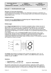
LAB 2 Design and Simulation of Sequential Logic Circuits - Synchronous Counters - 1. Purpose: This lab will enable students gain practice in the conversion of functional requirements into logic circuits and their implementation using on the Altera DE2-115 board. The purpose of this lab is to introduce students to the design of sequential circuits based on Altera’s Quartus development environment and their implementation and testing with an FPGA. Enter the design of synchronous counters using Quartus II graphics editor Assign the input-output pins and prepare the design for downloading and testing on the Altera DE2-115 board Test the counter: - Display the counter outputs as binary values on LEDs - Using an oscilloscope, trace and record the waveforms at various flip-flops. 2. Requirements of the Lab: The following results need to be submitted in your report. * The log of what you did * The screen shots of all schematics and all waveform diagrams * Compilation, simulation and downloading messages (if any) * Your test results 3. Equipment and Supplies: * Quartus II (web edition) * Altera DE2-115 board with - USB-Blaster cable - Power supply 12V/2A *Probe *Coaxial cable *Wires *Ribbon cable 4. References: i. Chapter1 and 2 of the Text book: Computer Systems Architecture, Morris Mano, 3rd Ed ii. DE2-115 User Manual posted in the Documentation section under the Laboratories tab of CEG2136 Virtual Campus. 5. PreLab For each of the following counters (a. and b.): Draw the state diagram and derive the excitation table for all the flip-flops involved in the counter (the excitation table for counter a. is already given below), Derive and simplify the Boolean expression of every flip-flop input using Karnaugh maps. CEG 2136 Lab 2 a. Page 2 of 10 3 bit synchronous modulo 6 counter Block diagram in Fig. 1.(a), has to observe the following counting sequence: 000 --> 010 --> 110 --> 011 --> 101 --> 100 --> 000. This counter is to be implemented with JK flip flops which have active-low asynchronous Reset inputs (CLRN); the flip-flops’ clock inputs (CLK) are connected all together to CCLK (counter clock). Present Next Synchronous State State Inputs msb lsb msb lsb msb lsb Q2 Q1 Q0 Reset Q Q Q Q Q Q J K J K J 2 1 0 2 1 0 2 2 1 1 0K0 CCLK 000 010 0x 1x 0x 001 xxx xx xx xx 010 110 1 x x 0 0x 010 110 011 101 1x x1 x0 000 100 000 x 1 0 x 0x 011 101 100 x0 0x x1 100 101 110 011 x1 x0 1x 111 xxx xx xx xx Figure 1: (a) Block diagram and (b) State Diagram of a Modulo 6 counter Table 1: The Excitation Table for the JK flip-flops Modulo 6 counter b. 4-bit synchronous BCD counter 0000 --> 0001 --> 0010 --> 0011 --> 0100 --> 0101 --> 0110 --> 0111 --> 1000 --> 1001 --> 0000 --> … PART I (Design and simulation) To capture your design in the Altera’s development environment you can use Quartus’ “New Project Wizard” or you can proceed manually with the following design flow. For each circuit designed above (3 bit modulo 6 and 4-bit BCD synchronous counters): 1. Draw the circuit diagrams using the graphics editor of Quartus in a schematic file and save the corresponding .bdf file. Use the counter’s signal names suggested in the block diagram (Figure 1. a) when editing the names of the pins of your circuit. In the Project Navigator pane select the Files tab; rightclick on your schematic file (.bdf) and select Set as Top Level Entity Also save the schematics as a jpeg file or print it for inclusion in your report. 2. To assign EP4CE115F29C7 to your project go to Assignments in the main menu, select Device and in the window Settings chose Cyclone IV E for the Device Family and then from the list of Available Devices choose EP4CE115F29C7. EECS Fall 2015 2 Page 3 of 10 CEG 2136 Lab 2 In the main menu select Processing Start compilation or click on the toolbar icon ► or press Ctrl+L. 3. To visualize the input and output signals of your counter (clock, reset, flipflops’ outputs) you have to create a University VWF file where you will catch the time diagram of these signals. 4. To define the set of pins of your test circuit, while in the .vwf tab, do select in the main menu Edit >> Insert >> Insert Node or Bus… and click on Node Finder. 5. In the option Filter of the popped-up Node Finder window choose ‘Pins: All’, then click on the button List and move all found nodes (from the left list) to the right pane by clicking , then press OK to return to your .vwf files. 6. To set time characteristics of the simulation clock click on the clock signal (CCLK) to select it, then do Edit >> Value>> Clock and in the Clock window put a Period of 20 ns (a close approximation of the DE2-115 board clock)… and click OK. Make sure you assign logic 1 to Reset by Forcing High (1), to allow your counter operates under the CCLK control. At this point you can run a functional simulation. The binary representation of the counter’s states can be displayed by grouping Q2 – Q0 in a bus. 7. To choose a grid of 20 ns do: Edit >> Grid Size, then put 20 ns for Period. Run your simulation (Processing Start simulation or click on the toolbar icon ) and inspect the time diagram of your Simulation Report – Simulation Waveforms window and verify if your synchronous counter follows the given counting sequence; if it doesn’t, verify your equations and/or debug your circuit. NOTE: Make sure that under the simulator is the Quartus II simulator. Under Simulation menu, go to Options and select Quartus II Simulator as the simulator. Show the simulation to your instructor and capture it in a graphic format for your lab report (copy to clipboard all the waveforms and paste them into a .doc file); to get a better visualization of your waveforms, you may want to change the time base in your .vwf file by choosing in Edit/End Time a Time EECS Fall 2015 3 Page 4 of 10 CEG 2136 Lab 2 = 0.5 μs). Show the design and demonstrate the simulations to your TA. PART II (Testing experiment) Two (different speed) approaches can be considered to experimentally test the counters designed above: II-1. Automatic, free running (highest speed) - by connecting CCLK to the DE2115 board general clock (GCLK1 - generated on board) and visualizing the flip-flops’ outputs with an oscilloscope. II-2. Manual control - by deriving CCLK from a push-button and displaying the flip-flops’ outputs on LEDs as shown below (block diagram of Figure 2). II-1. Automatic free running counter In this mode you can visualize the signals of your real circuit by employing an oscilloscope. The real signals should be similar to the waveforms you obtained by simulating your circuit in PART I. 1. Return to your .bdf file and from File >> Create/ Update >> Create Symbol Files For Current File you can create a symbol (.bsf file) for your synchronous counter. 2. Now you can create a test circuit for the counter with the Quartus graphic editor (test1.bdf). Save the file and set the project to the current file with Set as Top Level Entity. The counter Symbol created above can be inserted into your schematics by going Edit >> Insert Symbol and looking for it in the Project directory of the Symbol Libraries. The clock input of the counter (clk) has to be connected to the system clock (GCLK1 - from the on-board oscillator of 50MHz) that is directly connected to the FPGA PIN Y2. Remember to compile your file before assigning the pins! 3. Assign the EP4CE115F29C7 device number to your design (Assign/Device) and then assign pin numbers as shown in Table 2. EECS Fall 2015 4 Page 5 of 10 CEG 2136 Lab 2 Table 2: Free-running Pin Assignment Value GCLK Q3 Pin assignment PIN_Y2 PIN_Y17** Component 50MHz oscillator Oscilloscope output*** Q2 PIN_AB21** Oscilloscope output*** Q1 Q0 PIN_AC15** PIN_AB22** Oscilloscope output*** Oscilloscope output*** RESET CLKOUT* PIN_AB28 PIN_AE23 SW0 SMA_CLKOUT *In order to have the 50MHz clock as output create a CLKOUT signal and assign its value to GCLK. **You can select a different output pin but following the GPIO pin assignment below. ***When viewing the oscilloscope output, you will need to connect a ground to your probe (to close the loop). Select pin right 15 (from top) as your ground. Figure 2: GPIO 40-pin assignments a. Select Assignments Assignment Editor; under Category select ALL. b. Double-click on the entry <<new>> in the column labeled To. Press the binoculars to open the Node finder window, then select i. Filter Pins: all, then click on List. ii. Select (highlight) GCLK1, Q3, Q2, Q1, Q0 and RESET from the left column of Nodes Found and then click on “>” to have all GCLK1, Q3, Q2, Q1, Q0 and RESET in the right Selected Nodes column. The EECS Fall 2015 5 Page 6 of 10 CEG 2136 Lab 2 content of the left column is entirely copied to the right (without having to select them) by simply hitting “>>”. Click OK to close the Node Finder window. c. Compile your project with the assigned pins. 4. Make sure the RUN/PROG switch (SW19; leftmost toggle switch) is set to RUN. 5. Select Tools Programmer in the Quartus II window. From Hardware Settings, in the Currently Selected Hardware box, select USB-Blaster and click Close. NOTE: if the USB-Blaster doesn’t show-up in the list of Currently Selected Hardware, close the window and open it again. You might have to repeat this process a few times. 6. In the Programmer window, check that the *.sof file is listed. If it is not then click the Add File button on the left panel and look for the *.sof file under the …/output_files directory in the current working directory. 7. Make sure Program/Configure is checked-in. Click Start and verify your circuit. Remember that a LED illuminates when its control input is 1. NOTE: Once done you do not need to save the *.cdf file. 8. Use an oscilloscope to visualize the clock and the flip-flops’ outputs. Connect the probe of oscilloscope channel 1 to one of your ribbon cable pins that maps to your counter pin assignments (one-by-one) and use the coaxial cable to output the clock signal. Draw these time diagrams. Measure the rising and falling times of your signals. Hint: Under Measure menu on the oscilloscope, select the Meas push-button. Make sure channel 2 is selected. Select the Type on-screen menu and search for Snapshot all option. When select the Add measurement option it will display all the necessary values you will need. NOTE: How to use the oscilloscope: When turning on the oscilloscope, wait a few minutes (it takes time to boot-up). Once the oscilloscope is powered-on, select channel 2 (channel on which the probe is on) and select the Probe menu on screen (use the push-buttons below to select the Probe menu). Once Probe menu is selected, change the probe Ratio to 10:1V (use the control knob under the green arrow named Push to select). EECS Fall 2015 6 Page 7 of 10 CEG 2136 Lab 2 II-2. Manual control For this mode you have to derive the counter’s clock CCLK from a push-button (KEY0) and displaying the flip-flops’ outputs on LEDs as shown below (block diagram of Figure 3). Figure 3: COUNTER test circuit The DE2-115 board provides four push-button switches as shown in Figure 3. Each of these switches is debounced using a Schmitt Trigger circuit, as indicated in Figure 4. The four outputs called KEY0, KEY1, KEY2, and KEY3 of the Schmitt Trigger devices are connected directly to the Cyclone IV E FPGA. Each push-button switch provides a high logic level when it is not pressed, and provides a low logic level when depressed. Since the push-button switches are debounced, they are appropriate for using as clock or reset inputs in a circuit. [1] In the past, student were provided with FPGA boards where the push-buttons where mechanical switches. Therefore, they had to add a debouncer in order to correct the oscillation encountered while pushing on the mechanical switches. For more information, see Appendix A. Figure 4: Block diagram of 4 push-button on DE2-115 boards EECS Fall 2015 7 Page 8 of 10 CEG 2136 Lab 2 Figure 5: Debouncing mechanism (Schmitt Trigger) 1. Return to your .bdf file and from File >> Create/ Update >> Create Symbol Files For Current File you can create a symbol (.bsf file) for your synchronous counter. Table 3: Manual Control Pin Assignment Value CCLK Q3 Pin assignment PIN_M23 PIN_E24 Component KEY0 LEDG3 Q2 PIN_E25 LEDG2 Q1 Q0 PIN_E22 PIN_E21 LEDG1 LEDG0 RESET PIN_AB28 SW0 2. Assign the EPM7128SLC84-7 device number to your design (Assign/Device) and then assign pin numbers as shown in Table 3. Select Assignments Assignment Editor; under Category select ALL. 3. Double-click on the entry <<new>> in the column labeled To. Press the binoculars to open the Node finder window, then select a. Filter Pins: all, then click on List. b. Select (highlight) CCLK, Q3, Q2, Q1, Q0 and RESET from the left column of Nodes Found and then click on “>” to have all CCLK, Q3, Q2, Q1, Q0 and RESET in the right Selected Nodes column. The content of the left column is entirely copied to the right (without having to select them) by simply hitting “>>”. Click OK to close the Node Finder window. 4. Compile your project with the assigned pins. EECS Fall 2015 8 Page 9 of 10 CEG 2136 Lab 2 5. Make sure the RUN/PROG switch (SW19; leftmost toggle switch) is set to RUN 6. Select Tools Programmer in the Quartus II window. From Hardware Settings, in the Currently Selected Hardware box, select USB-Blaster and click Close. NOTE: if the USB-Blaster doesn’t show-up in the list of Currently Selected Hardware, close the window and open it again. You might have to repeat this process a few times. 7. In the Programmer window, check that the *.sof file is listed. If it is not then click the Add File button on the left panel and look for the *.sof file under the …/output_files directory in the current working directory. 8. Make sure Program/Configure is checked-in. Click Start and verify your circuit. Remember that a LED illuminates when its control input is 1. NOTE: Once done you do not need to save the *.cdf file. 9. Find experimentally the count table of your synchronous counter by pressing the KEY0 pushbutton until you rollover a full counting sequence. Verify that the output of your synchronous counter matches the corresponding state diagram you were initially given. 10. Demonstrate the operation of your circuit to your instructor. References 1. “DE2-115 User Manual,” Terasic Technologies Inc., http://www.terasic.com.tw/cgibin/page/archive.pl?Language=English&CategoryNo=165&No=502&PartNo=4 , 2013 EECS Fall 2015 9 Page 10 of 10 CEG 2136 Lab 2 APPENDIX A: Switch debouncing In the past, students were given an Altera UP2 board. On those boards, two push-buttons (MAX_PB1 and MAX_PB2) provide active-low signals and are pulled-up through 10-KΩ resistors, as shown in Figure 1. When the contacts of any mechanical switch bang together, they rebound a bit before settling, causing bounce and generating an uncontrolled number of oscillations before coming to a still, as shown in the time diagram of Figure 2. MAX_PB1 Figure 2: High-to-low switch transitory oscillations Debouncing is the process of removing those bounces and generating a single pulse (preferably synchronous with the system’s clock), as soon as a steady stable contact is made. Figure 1: Pull-up resistors To correct such issue, they used the debounce.tdf module that describes a debouncing circuit in a Hardware Description Language. While implementing it on the CPLD, it will generate a single pulse after a delay which is triggered by the rising-edge of any oscillation of the switch MAX_PB1 (i.e., at the end of pressing MAX_PB1); where the delay duration has to be greater than the time between two parasitic pulses (Figure 3). MAX_PB1 t pulse t Figure 3: Time diagram of single pulse generator debounce module. You will learn more about switch debouncing in CEG3136 (Computer Architecture II). EECS Fall 2015 10