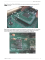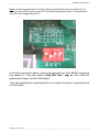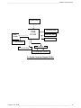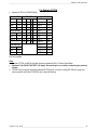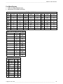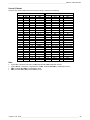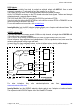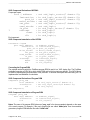
1
MATrix-II VLSI Protoboard User’s Manual Rev : 3 ni logic Pvt. Ltd. (ni2designs) 201/202, C-2, Saudamani Commercial Complex, Bhusari Colony, Paud Road, Kothrud, Pune-411 038 Telefax : +91-20-25286947/8 [email protected] www.ni2designs.com ___________________________________________________________________________________ MATrix-II VLSI Protoboard Preface: This manual is for the users of MATrix-II with in-depth details of product including reference designs and examples. Copyrights: We acknowledge that the following organizations claim trademark rights in their respective products or services mentioned in this document, specifically: Altera, Quartus-II, ACEX, ByteBlaster, etc Xilinx, ISE, iMPACT, Spartan-II, etc. For further details and queries contact: ni logic Pvt. Ltd. (ni2designs) 201/202, C-2, Saudamani Commercial Complex, Bhusari Colony, Paud Road, Kothrud, Pune-411 038 Telefax : +91-20-25286947/8 [email protected] www.ni2designs.com ni logic Pvt. Ltd., Pune___________________________________________________________________________________ 2 ___________________________________________________________________________________ MATrix-II VLSI Protoboard MATrix-II VLSI Protoboard User Manual Rev : 3 Table of Contents 1. Introduction a. Introduction to Programmable logic and PLDs b. Product Introduction 2. Features and Specifications 3. Getting Started 4. Diagrams a. I/O Connections for Xilinx FPGA b. I/O Connections for Altera FPGA c. I/O Connections for CPLDs d. Baseboard legend diagram 5. Precautions 6. Design Flow a. PLD design flow b. Microcontroller design flow c. Xilinx webpack design flow d. Altera Quartus-II design flow e. Keil design flow 7. Configuration/Downloading a. Types of Modes b. Jumper setting for mode selection c. Using Variable frequency generator d. Programming Atmel Microcontroller 8. Pin Assignments 9. Jumper settings 10. Using External Adaptors 11. How to use Pico-blaze 12. Sample codes 13. Glossary 14. Global Design Hints 15. Troubleshooting 16. Device Features ni logic Pvt. Ltd., Pune___________________________________________________________________________________ 3 ___________________________________________________________________________________ MATrix-II VLSI Protoboard Chapter 1: Introduction 1.a What is Programmable Logic? In the world of digital electronic systems, there are three basic kinds of devices: memory, microprocessors, and logic. Memory devices store random information such as the contents of a spreadsheet or database. Microprocessors execute software instructions to perform a wide variety of tasks such as running a word processing program or video game. Logic devices provide specific functions, including device-to-device interfacing, data communication, signal processing, data display, timing and control operations, and almost every other function a system must perform. Fixed Logic versus Programmable Logic Logic devices can be classified into two broad categories - fixed and programmable. As the name suggests, the circuits in a fixed logic device are permanent, they perform one function or set of functions - once manufactured, they cannot be changed. On the other hand, programmable logic devices (PLDs) are standard, off-the-shelf parts that offer customers a wide range of logic capacity, features, speed, and voltage characteristics - and these devices can be changed at any time to perform any number of functions. With fixed logic devices, the time required to go from design, to prototypes, to a final manufacturing run can take from several months to more than a year, depending on the complexity of the device. And, if the device does not work properly, or if the requirements change, a new design must be developed. The up-front work of designing and verifying fixed logic devices involves substantial "non-recurring engineering" costs, or NRE. These NRE costs can run from a few hundred thousand to several million dollars. With programmable logic devices, designers use inexpensive software tools to quickly develop, simulate, and test their designs. Then, a design can be quickly programmed into a device, and immediately tested in a live circuit. There are no NRE costs and the final design is completed much faster than that of a custom, fixed logic device. Another key benefit of using PLDs is that during the design phase customers can change the circuitry as often as they want until the design operates to their satisfaction. That's because PLDs are based on re-writable memory technology - to change the design, the device is simply reprogrammed. Once the design is final, customers can go into immediate production by simply programming as many PLDs as they need with the final software design file. CPLDs and FPGAs The two major types of programmable logic devices are field programmable gate arrays (FPGAs) and complex programmable logic devices (CPLDs). Of the two, FPGAs offer the highest amount of logic density, the most features, and the highest performance. The largest FPGA provides millions of “system gates" (the relative density of logic). These advanced devices also offer features such as built-in hardwired IP cores (such as the IBM Power PC, PCI cores, microcontrollers, peripherals, etc), substantial amounts of memory, clock management systems, and support for many of the latest, very fast device-to-device signaling technologies. FPGAs are used in a wide variety of applications ranging from data processing and storage, to instrumentation, telecommunications, and digital signal processing. CPLDs, by contrast, offer much smaller amounts of logic - up to about 10,000 gates. But CPLDs offer very predictable timing characteristics and are therefore ideal for critical control applications. Low power CPLDs are also available and are very inexpensive, making them ideal for cost-sensitive, battery-operated, portable applications such as mobile phones and digital handheld assistants. The PLD Advantage Fixed logic devices and PLDs both have their advantages. Fixed logic devices, for example, are often more appropriate for large volume applications because they can be mass-produced more economically. For certain applications where the very highest performance is required, fixed logic devices may also be the best choice. ni logic Pvt. Ltd., Pune___________________________________________________________________________________ 4 ___________________________________________________________________________________ MATrix-II VLSI Protoboard However, programmable logic devices offer a number of important advantages over fixed logic devices, including: PLDs offer customers much more flexibility during the design cycle because design iterations are simply a matter of changing the programming file, and the results of design changes can be seen immediately in working parts. PLDs do not require long lead times for prototypes or production parts - the PLDs are already on a distributor's shelf and ready for shipment. PLDs do not require customers to pay for large NRE costs and purchase expensive mask sets - PLD suppliers incur those costs when they design their programmable devices and are able to amortize those costs over the multi-year lifespan of a given line of PLDs. PLDs can be reprogrammed even after a piece of equipment is shipped to a customer. In fact, thanks to programmable logic devices, a number of equipment manufacturers now have the ability to add new features or upgrade products that already are in the field. To do this, they simply upload a new programming file to the PLD, via the Internet, creating new hardware logic in the system. Conclusion The value of programmable logic has always been its ability to shorten development cycles for electronic equipment manufacturers and help them get their product to market faster. As PLD suppliers continue to integrate more functions inside their devices, reduce costs, and increase the availability of time-saving IP cores, programmable logic is certain to expand its popularity with digital designers. 1.b Product Information The MATrix-II ( Multiple Application Tricks) is a low cost universal platform for testing and verifying designs based on the Xilinx and Altera PLDs. The purpose of MATrix-II is to teach the basic concepts of VLSI designing along with various electronics circuits. The MATrix-II has been revised and also extended to some basic electronic circuits for application development and their realization. Using this protoboard the user can verify his PLD designs with complete applications and also it gives a complete set of modules for project development for final year students. MATrix-II supports multiple vendor devices from Xilinx and Altera, who are world leader in PLD manufacturing. The MATrix-II supports Spartan-2 and XC9500 series of devices from Xilinx; and ACEX 1K and MAX7000s series of devices from Altera. The basic version of MATrix-II comes with 50,000 gate XC2S50-PQ208 FPGA, XC9572 or MAX7128S CPLD and EP1k50TQ144 FPGA from Altera along with supporting circuitry to ease prototype efforts (optional PLD modules available). MATrix-II comes along with various adaptors, which are optional to user. Every adaptor is pluggable with baseboard with the help of connectors. 1. 2. 3. 4. 5. 6. Keypad adaptor LCD adaptor Dot matrix rolling display card Relay card 89C51 adaptor ADC/DAC adaptor With these adaptors user expands his choice and features to prototype and solve his design needs and requirements. Above modules are optional to the baseboard and can be used by plugging into it. ni logic Pvt. Ltd., Pune___________________________________________________________________________________ 5 ___________________________________________________________________________________ MATrix-II VLSI Protoboard Chapter 2: Features & Specifications 2.a Features and Specifications Multi-vendor device support for Xilinx and Altera PLDs. Packages supported PLCC84, TQ144 and PQ208. Upto 140 user I/Os. Voltage support to +1.2V, +2.5V, +3.3V & +5V devices, All FPGA I/Os accessible through headers. Four Multiplexed 7-Segment displays (with segment map). Interface to RS232 with 9-pin D-type connector. User selectable configuration modes, using FLASH PROM / JTAG / Slave Serial. Byte-blaster cable interface for configuration of Altera FPGAs. On board 8-MHz Clock oscillator (user selectable). Variable frequency generator (from 100 Hz to 10 KHz range). Higher frequency board support. Configurable 24 switches as I/P or O/P. 16 digital LED indicated outputs. Power on Reset and configuration reset key. Support for different I/O Standards. 4x4 Keyboard matrix card. Interface to Atmel AT89s8252 microcontroller. Facility for I2C interface. 8-bit ADC/DAC add-on card. Four 5x7 Dot Matrix displays. Optically isolated relay card. 16x2 character LCD display with contrast control. Short circuit protection circuit. ni logic Pvt. Ltd., Pune___________________________________________________________________________________ 6 ___________________________________________________________________________________ MATrix-II VLSI Protoboard 2.b Individual Module Specification * Keyboard adaptor o 4x4 membrane keypad Liquid Crystal Display (LCD) adapter o 16 x 2 characters LCD display with Contrast control Relay Card o 2 Optically isolated relays o NC, NO, COMM I/Os on power header o Relay ON indication Dot Matrix rolling display panel o Matrix of four 5x7 LED display o Total 140 LED matrix on board. Pluggable Micro controller Card o Atmel AT89S8252 ISP microcontroller o 8KB ISP Flash & 2KB of EEPROM. o Coupled with FPGA for embedded application development. o All 32 I/O lines accessible to FPGA. o On board reset circuit o Timer, interrupt and ISP ports. ADC/DAC Card o 8 channel ADC 0809 with sampling speed of 20KHz on single channel. o Single channel DAC0800 with 150ns settling time. o Facility for onboard gain and reference voltage adjustment. Xilinx CPLD Module o XC9572 PC84-15C containing 72 macrocells with 1,600 usable gates. Xilinx FPGA Module o 50,000 gate density XC2S50 PQ208-5 FPGA from Xilinx. Altera CPLD Module o EPM7128SLC84-15C device containing 128 macrocells with 2,500 usable gates. Altera FPGA Module o 50,000 gate density EP1K50 TQ144-3C FPGA from Altera. *Note: Above module are optional with the product. ni logic Pvt. Ltd., Pune___________________________________________________________________________________ 7 ___________________________________________________________________________________ MATrix-II VLSI Protoboard Power supply Required voltages are generated onboard through regulators; other supply voltages are applied from external power supply. Here is the list of voltages on board used. +12V +5V -5V +3.3V +2.5V +1.2V * Note: The above specifications and features of product are subject to change with new versions of product. Connectors Header Name Relay Header Digital I/Os and Rolling display 8051 Header LCD Header ADC/DAC & Keypad PLD Header Power supply Ident JP5 JP3 JP2 JP4 JP1 JH1, JH2, JH3, JH4 JP6 Jumpers Jumpers are provided on baseboard for selection of 1. Configuration mode pins 2. Bypassing the PROM 3. Selecting configurable Input or Output 4. Selecting the O/P LEDs. o J8-J11 Mode selection headers o J6, J7 PROM bypass o S0-S7 SW1 o S8-S15 SW2 o S16-S23 SW3 Downloading cable For Xilinx PLDs For configuration of Xilinx FPGA and CPLD from PC, a 9 pins D Type connector is provided on baseboard. The MATrix can be connected to PC's parallel port with cable provided having 25 pins D Type connector on other end. For Altera PLDs Altera PLD adaptors have onboard JTAG header. User has to connect the programming JTAG cable provided on this header and other end to PCs parallel port to configure the PLDs. *Note: Kindly remove the cables by its headers only. Removing the cables by handling its wire may cause damage to its joints. ni logic Pvt. Ltd., Pune___________________________________________________________________________________ 8 ___________________________________________________________________________________ MATrix-II VLSI Protoboard Chapter 3: Getting Started After going through this chapter user will be able to start using board with ease. A user has to see this chapter as introduction to steps involved in using the board, its handling and programming of the devices. Step 1:. Connect the power cable to the Universal board as shown in figure. Applying Power to the Board To power-up the Universal board place switch in the ON position. When power is supplied to the Universal board, LED D1 turns on, indicating the board has power. Step 2:- Connect the programming cable on programming port as shown in figure.. Programming Port Connect the JTAG cable DB 9 pin male plug to DB 9 pin Female connector on programming port P2 and connect the other end to the parallel port on your PC This allows you to directly configure the Xillinx PLD . ni logic Pvt. Ltd., Pune___________________________________________________________________________________ 9 ___________________________________________________________________________________ MATrix-II VLSI Protoboard Step 3:- Plug the Xilinx FPGA (XC2S50 PQ208) card on base board (white dot should be match both PLD card and baseboard). Step 4:- Make the jumper settings for programming mode as shown in figure below (short 2-3). These jumper block settings control the FPGA’s configuration mode or PROM Configuration mode. As per the settings below, the Xilinx FPGA or CPLD would be programmed in Boundary scan or JTAG mode. ni logic Pvt. Ltd., Pune___________________________________________________________________________________ 10 ___________________________________________________________________________________ MATrix-II VLSI Protoboard Step 5:- Set the programming mode to JTAG by setting the mode selection switch into position shown as below. This switch (SW6) is used to put the FPGA in the different programming mode. It is recommended to use JTAG mode for programming from PC. At this point your board is ready to accept programming file from Xilinx iMPACT programmer from desktop PC. Now refer chapter “Using EDA Tools”, page no. 19 to follow the implementation steps of the Xilinx ISE software. There after generating the programming file from it, program the device on board and check your functionality. ni logic Pvt. Ltd., Pune___________________________________________________________________________________ 11 ___________________________________________________________________________________ MATrix-II VLSI Protoboard Chapter 4: Diagrams 8051 Header LCD Header ADC/DAC Keypad Header Config. Reset Dot Matrix Display and I/Os Functional Reset Spartan-II FPGA PQ208 Relay Header Clock Osc. (8 MHz) Var. Clock (in KHz) 7 Seg. Displays 16 O/P LEDs RS-232 Jumpers 24 configurable switches 4.a System Connection Diagram (Xilinx FPGA) ni logic Pvt. Ltd., Pune___________________________________________________________________________________ 12 ___________________________________________________________________________________ MATrix-II VLSI Protoboard ADC/DAC Keypad Header Dot Matrix Display and I/Os Functional Reset ACEX1K FPGA TQ144 Relay Header Clock Osc. (8 MHz) Var. Clock (in KHz) 7 Seg. Displays RS-232 16 O/P LEDs Jumpers 24 configurable switches 4.b System Connection Diagram (Altera FPGA) ni logic Pvt. Ltd., Pune___________________________________________________________________________________ 13 ___________________________________________________________________________________ MATrix-II VLSI Protoboard Keypad Header Functional Reset CPLD PLCC84 Relay Header Clock Osc. (8 MHz) Var. Clock (in KHz) 7 Seg. Displays 16 O/P LEDs Jumpers 24 configurable switches 4.c System Connection Diagram (CPLDs) ni logic Pvt. Ltd., Pune___________________________________________________________________________________ 14 ___________________________________________________________________________________ MATrix-II VLSI Protoboard 4d MATrix board component legend diagram RS-232 Port Prog. Port Configurable I/Os Configuration Mode Selection Rolling Display Regulators Relay Header 7 segment Displays ni logic Pvt. Ltd., Pune___________________________________________________________________________________ 15 ___________________________________________________________________________________ MATrix-II VLSI Protoboard Chapter 5: Precautions Verify the power on LED status after applying power to the trainer. Connect the 9 pin D connector of the cable to the trainer only after confirming the above During downloading make sure that the jumper selections are proper. Select the proper configuration mode during programming, else programming can fail. Take care for adaptor position before plugging on the board; this may cause damage to PLD device on power ON if plugged incorrectly. Insert the PLD adaptor by looking at the circle marks given on the baseboard and adaptor card. Do not touch the FPGA, as your body static charge may damage FPGA. Before implementation, it is necessary to lock the pins in user constraint file (UCF) as per the design and I/Os used. For downloading the bit stream, the downloading circuit requires a stable supply; hence it is recommended to use power supply given along with the trainer board. PLD devices are sensitive to surge currents and voltages. The devices supported on MATrix works 5V logic family, user can read device datasheets before applying external signals to device. Kindly remove the cables from holding its headers only. Removing the cables from holding its wires may cause damage to cable joints. ni logic Pvt. Ltd., Pune___________________________________________________________________________________ 16 ___________________________________________________________________________________ MATrix-II VLSI Protoboard Chapter 6: Design Flow Design Entry HDL (Verilog, VHDL) Hardware Description Language. Very High speed Integrated circuit HDL. Verilog having ‘C’ based constructs. Simulation Functional Verification Functional simulation of the design. No timings are considered. Synthesis Process for converting design specifications into gate level netlist. Needs synthesis library containing target technology information. Implementation Combined name for processes like for translation, floorplanning, mapping, place & route, bit file generation. For locking input and output signal to the particular pins of the device user must write UCF (User Constraint File) before implementation. Output of implementation is .BIT for FPGA and .JED file for CPLD, which can be directly program into the target device. Programming This is the process by which user can physically download the design programming files from PC to target device using programming cable. To program CPLD, select Boundary scan (JTAG) mode. To program FPGA, select Boundary scan, slave serial mode or Master serial Mode. ni logic Pvt. Ltd., Pune___________________________________________________________________________________ 17 ___________________________________________________________________________________ MATrix-II VLSI Protoboard Microcontroller Design Flow Source Code Entry Compile High-level language program description. Using assembly or ‘C’ language. Converters the object code to low-level language. Build Builds the programming hex file. Debug Step-by-step execution of program. Program Program the controller, using ISP/external programmer. ni logic Pvt. Ltd., Pune___________________________________________________________________________________ 18 ___________________________________________________________________________________ MATrix-II VLSI Protoboard Using EDA Tools In this chapter we will see how a project can be created in Xilinx and Altera EDA tools, and how we can proceed to use MATrix to perform our experiments. We take the example of half adder and implement on both vendor devices. Design flow for Xilinx ISE series softwares Step 1: Open ISE webpack software. Step 2: Create new project Step 3: Go to project menu and select new source ni logic Pvt. Ltd., Pune___________________________________________________________________________________ 19 ___________________________________________________________________________________ MATrix-II VLSI Protoboard Step 4: Select VHDL source file, name it adder, click next, and enter entity I/Os as A, B, Sum & Carry. Step 5: Write VHDL code for half adder. ni logic Pvt. Ltd., Pune___________________________________________________________________________________ 20 ___________________________________________________________________________________ MATrix-II VLSI Protoboard Step 6: Create new source file for implementation constraint file. Name it adder_UCF, and associate with the corresponding design file. Step 7: To assign the pin location of the design, open the UCF file, to run the constraint editor where we have to lock the I/Os of design to a particular pin number. ni logic Pvt. Ltd., Pune___________________________________________________________________________________ 21 ___________________________________________________________________________________ MATrix-II VLSI Protoboard Step 8: Once the constraint editor is open, goto ports tab, and assign the pins by referring the Pin assignment chapter. Eg: net A loc =p82; Step 9: Save the UCF file and come back to project navigator. Now selecting the adder design file, run the synthesis process, there after Implementation and finally run generate programming file option. ni logic Pvt. Ltd., Pune___________________________________________________________________________________ 22 ___________________________________________________________________________________ MATrix-II VLSI Protoboard Step 10: After the all the three processes are successfully over, run the configure device (impact) option to open the impact programmer. After opening impact add Xilinx device design file, for CPLD it is *.jed file, and for FPGA it is *.bit file. Step 11: Go to operations option and select program option. ni logic Pvt. Ltd., Pune___________________________________________________________________________________ 23 ___________________________________________________________________________________ MATrix-II VLSI Protoboard Step 12: Keep the erase option enabled and click OK. Step 13: After erasing the CPLD, the programming would start and will configure the particular device. Now check the functionality on the board and verify it by applying different inputs to FPGA from switches on board. ni logic Pvt. Ltd., Pune___________________________________________________________________________________ 24 ___________________________________________________________________________________ MATrix-II VLSI Protoboard Design Flow for Quartus-II series of software of Altera. Install Quartus-II (version 3.0 & above) software on your machine, the supported platforms are windows NT/XP/2000. We take the same half adder example for implementing on the Altera MAX7000s CPLD. Step 1: Start Quartus-II (version 3.0 & above) software. Step 2: For new project creation, go to File option and select new project wizard. In the opened window, specify project location and design and entity name. For eg. Entity name adder, and top design name also adder. Click “next”. ni logic Pvt. Ltd., Pune___________________________________________________________________________________ 25 ___________________________________________________________________________________ MATrix-II VLSI Protoboard Step 3: Click “next” button till you reach EDA tool settings window, there keep all options as none, which in default will select the inbuilt design tools and softwares for the design processing. Click “next”. Step 3: Select MAX700S device family in the next window. Click “next”. ni logic Pvt. Ltd., Pune___________________________________________________________________________________ 26 ___________________________________________________________________________________ MATrix-II VLSI Protoboard Step 4: In the next window, select the device as EPM7128SLC84-15. Click “next”. Step 5: Click “Finish”. And the new project would be created. Now we need to make and add new design file in the project. So goto “File” menu, and click “New“, and select VHDL File, in the “device design files” tab. Click “OK”. ni logic Pvt. Ltd., Pune___________________________________________________________________________________ 27 ___________________________________________________________________________________ MATrix-II VLSI Protoboard Step 6: Write the VHDL code for half adder design, and save the file as “adder.vhd” Step 7: Now goto processing menu- then – start -, click start analysis and synthesis. ni logic Pvt. Ltd., Pune___________________________________________________________________________________ 28 ___________________________________________________________________________________ MATrix-II VLSI Protoboard Step 8: Read the synthesis reports Step 9: For performing simulation, we need to create stimuli file from where we can apply input signals and watch the o/p waveforms. Goto file menu, and click new file, goto other files tab, and select “vector waveform file” option. ni logic Pvt. Ltd., Pune___________________________________________________________________________________ 29 ___________________________________________________________________________________ MATrix-II VLSI Protoboard Step 10: Add the entity signals in the waveform window, and apply different sets of value to check the functionality. Save the file as the same name of entity, adder.vwf Step 11: In Altera Quartus-II software you can perform Functional and Timing simulation. For simulation mode settings, for to assignments menu, and click settings. ni logic Pvt. Ltd., Pune___________________________________________________________________________________ 30 ___________________________________________________________________________________ MATrix-II VLSI Protoboard Step 12: Now goto simulator setting, then to mode, and in the right-hand side window, select the simulation mode to Functional. Step 13: After clicking OK, come back to main window, and goto processing window, and click start simulation, the Quartus-II will start the simulation the result would appear in couple of minutes. Observe the results, if found bugs, then change VHDL code and start simulation again. ni logic Pvt. Ltd., Pune___________________________________________________________________________________ 31 ___________________________________________________________________________________ MATrix-II VLSI Protoboard Step 14: Once the simulation results found correct, then we need to implement the design in the target device. For this we need to lock our design I/Os with the Kit I/O pin details. Goto assignment menu, click “assign pin” option. Step 15: Looking at the pin assignment chapter, lock the MAX7000s CPLD I/O with the particular pin no., for this select the I/O number on the LHS, name the design I/O in the bottom pin name option, and then click add, the particular signal will be locked to that pin number ni logic Pvt. Ltd., Pune___________________________________________________________________________________ 32 ___________________________________________________________________________________ MATrix-II VLSI Protoboard Step 16: Once the pin assignment is over, come back to main window. Now we need to implement the design on the particular device. So goto processing menu, and click start compilation process. Which will fit the design in CPLD and generate the programming file. Step 17: Once the compilation process is over, user can check the reports and see the floorplan window. ni logic Pvt. Ltd., Pune___________________________________________________________________________________ 33 ___________________________________________________________________________________ MATrix-II VLSI Protoboard Step 18: Now we need to program CPLD, for this goto tools menu, and click programmer. Which will open the programmer; the software will automatically add the programming file (adder.pof). In the opened window select the program/configure option. Now we need to select the programming hardware, for which click the hardware tab on the LHS of programming window. Step 19: In the opened window Click add hardware tab, and select the hardware type as ByteBlasterMV or ByteBlaster II and port as LPT1. ni logic Pvt. Ltd., Pune___________________________________________________________________________________ 34 ___________________________________________________________________________________ MATrix-II VLSI Protoboard Step 20: Come back to hardware setup window, and click the select hardware tab and close the window. Step 21: Now click the start-programming button (play symbol) on the top LHS of the programming window (keep the program/configure option selected). ni logic Pvt. Ltd., Pune___________________________________________________________________________________ 35 ___________________________________________________________________________________ MATrix-II VLSI Protoboard Step 22: The programmer will start programming and in couple of seconds the device would be configured. Check the DONE indication in the bottom console window. Step 23: Check the design functionality on the board, by applying signal from switches or other points. ni logic Pvt. Ltd., Pune___________________________________________________________________________________ 36 ___________________________________________________________________________________ MATrix-II VLSI Protoboard Using Keil Compiler Designers can use compiler from Keil, one of the compilers available in market. Keil is a cross compiler supporting the 8051 based architecture controllers from various vendors. Compiler support the source codes written in ‘C’ and assembly languages. For starting up with MATrix, we have made a design flow guide for using the keil compiler, but for more information users can surf the help index of keil compiler, Install the Keil compiler from provided CD-ROM; you can use the evaluation version at start up, which supports the program code upto 2KB, which is sufficient for small development purposes. Step 1: Run the keil compiler EXE, which in turn will open the compiler. ni logic Pvt. Ltd., Pune___________________________________________________________________________________ 37 ___________________________________________________________________________________ MATrix-II VLSI Protoboard Step 2: Go to project menu and left click the new project option. Step 3: In the opened window user has to give project name and select the folder for the project creation, for example, name it keil demo. Click OK, and in the next window, you have to select the device to work on, the vendor name is Atmel, and the device number is 89S8252. The window will look like as below. ni logic Pvt. Ltd., Pune___________________________________________________________________________________ 38 ___________________________________________________________________________________ MATrix-II VLSI Protoboard Step 4: Click ok on the above window, and the project would be created. Now the user has to add or create the source code for the controller. For example for now designer can use the source code provided along with the code examples. So right click on source group and click add files to group. Step 5: Browse for the demo source code toggle.c and click add to insert it in the project. ni logic Pvt. Ltd., Pune___________________________________________________________________________________ 39 ___________________________________________________________________________________ MATrix-II VLSI Protoboard Step 6: User can have a look on the demo source code, which toggle Port 0, Port 1, and Port 2 after every 10ms. The source code is in ‘C’ language; users can also use assembly code for designing. Step 7: For building the program code or HEX code, we need to set some parameters in the compiler. Go to project options, and click option for target. ni logic Pvt. Ltd., Pune___________________________________________________________________________________ 40 ___________________________________________________________________________________ MATrix-II VLSI Protoboard Step 8: In the opened window, go to target tab, and in the window, set the Xtal frequency as 11.0592 MHz. Step 9: Now goto output tab and set the name of executable file as toggle; set the option create executable; and set create HEX file option. Finally click OK on the bottom side and come out of the window. ni logic Pvt. Ltd., Pune___________________________________________________________________________________ 41 ___________________________________________________________________________________ MATrix-II VLSI Protoboard Step 10: Now to build the HEX file, goto project menu, and click the build target option. This will generate the HEX file in the project folder, which you can use to program the controller using the provided Atmel ISP programming software. Source code for toggle program. 89c51 Source code: toggle.c HEX file : toggle.hex ni logic Pvt. Ltd., Pune___________________________________________________________________________________ 42 ___________________________________________________________________________________ MATrix-II VLSI Protoboard Chapter 7: Configuration/Downloading For Xilinx devices. Mode Selection Header J8 – J11 Slave Serial Short 1-2 JTAG Short 2-3 DIN TDI CCLK TCK PROG TMS DONE TDO Mode Selection Switch M0 M1 M2 JTAG 1 0 1 Slave Serial 1 1 1 Master Serial 0 0 0 The FLASH PROM is connected with FPGA through jumpers. While configuring the PLD from PC, the PROM has to be bypassed (JTAG & Slave serial modes). Jumper selection for PROM Bypass PROM Use PROM J6 Short 1-2 Short 2-3 J7 Short 1-2 Short 2-3 D0 EEPROM 3 2 1 Din TDO 3 2 TDI Din_FPGA FPGA J6 TDI_FPGA 1 J7 Note: Altera device adaptors can be programmed only in JTAG mode. For more programming details, refer the respective device datasheet. Using Variable Frequency Generator MATrix-II comes along with Variable Frequency Generator which users can use for low frequency applications, thus saving area and power. Also this Frequency Generator can be used for applying low frequency signals for time based applications. To use this signal as clock to PLD, do the following Short 1-2 pins of jumpers J4 & J5. Rotating the pot R50 in clockwise direction will decrease the frequency and vice-versa. To use it as signal, connect pin no. 1 of J4 header to any of the user I/O, then pin lock that I/O to the PLD and use in your application design. ni logic Pvt. Ltd., Pune___________________________________________________________________________________ 43 ___________________________________________________________________________________ MATrix-II VLSI Protoboard Programming Atmel Microcontroller Using the ISP programmer, designers can program the AT89S8252 controller. After building the HEX file from compiler, designers can refer the below shown steps to program the controller. Insert the controller module on MATrix baseboard; connect the cable provided to module and PC’s parallel port. Turn ON the power supply; now run the EXE of ISP programmer on your PC. Note: For win98 OS run ISP-Pgm3v0.exe, and for win NT/2000/XP OS run ISP-XP.bat batch file. The below shown window will open up. Features of Programmer: Supports AVR & 89s series of controllers. Security bit locking facility. Write & Read facility. Verification included during programming. Easy to use Step 1: Select the controller as AT89S8252 on the RHS of opened window. ni logic Pvt. Ltd., Pune___________________________________________________________________________________ 44 ___________________________________________________________________________________ MATrix-II VLSI Protoboard Step 2: Now Click the Open file button and browse to your project folder to open the currently created HEX in the programmer. Step 3: Now Click the Write button to program the device. User can also Write couple of times to ensure the write process. As this microcontroller module is connected directly with FPGA, so user has have to program the FPGA for feed through net program to get the signals from microcontroller and display on LEDs or some where else. For using this controller module on MATrix kit, users have to use FPGA as switch in between. Source code for toggle program. FPGA Source code: toggle_feed.vhdl Pin Lock file : toggle_feed_UCF.ucf Header Pin Details: J4 (Timer/Interrupts) Pin No. Signal 1 Int 0 2 Int 1 3 T0 4 T1 5 Ground J5 (ISP Header) Pin No. Signal 1 SCK 2 MISO 3 MOSI 4 RST 5 Ground ni logic Pvt. Ltd., Pune___________________________________________________________________________________ 45 ___________________________________________________________________________________ MATrix-II VLSI Protoboard Chapter 8: Pin Assignment For Xilinx Devices Spartan-II FPGA (XC2S30PQ208 or XC2S50PQ208 or XC2S200PQ208) XC9500 CPLD (XC95xx PC84) Clock and Reset FPGA CPLD Reset 206 74 L 15 Clock 80 10 L 14 L 13 Relay Header L 12 FPGA CPLD L 11 Relay 1 23 13 L 10 Relay 2 24 11 L 9 L8 RS-232 Port FPGA CPLD RXD 193 NA TXD 192 NA FPGA 45 46 47 48 49 57 58 59 O/P LEDs CPLD FPGA 35 L 7 61 36 L 6 62 37 L 5 63 39 L 4 67 40 L 3 68 41 L 2 69 43 L 1 70 44 L 0 71 7 segment Display CPLD FPGA CPLD 45 Seg A 27 34 46 Seg B 29 33 47 Seg C 30 32 48 Seg D 31 31 50 Seg E 33 26 51 Seg F 34 25 52 Seg G 35 24 53 Seg DP 36 23 DISP En 1 37 19 DISP En 2 41 17 DISP En 3 42 15 DISP En 4 43 14 NA: Not Available Note: The RS-232 port signals are being shared with FPGAs also, so if user is using RS-232 port along with microcontroller then those FPGA I/Os has to been left floating. ni logic Pvt. Ltd., Pune___________________________________________________________________________________ 46 ___________________________________________________________________________________ MATrix-II VLSI Protoboard For Xilinx Devices Spartan-II FPGA (XC2S30PQ208 or XC2S50PQ208 or XC2S200PQ208) XC9500 CPLD (XC95xx PC84) I/O S23 S22 S21 S20 S19 S18 S17 S16 FPGA 73 74 75 81 82 83 84 86 CPLD 54 55 56 57 58 61 62 63 Configurable Switches I/O FPGA CPLD S15 87 65 S14 88 66 S13 89 67 S12 90 68 S11 94 69 S10 95 70 S9 96 71 S8 98 72 I/O S7 S6 S5 S4 S3 S2 S1 S0 FPGA 99 100 101 102 108 109 110 111 CPLD 75 76 77 79 80 81 82 83 ni logic Pvt. Ltd., Pune___________________________________________________________________________________ 47 ___________________________________________________________________________________ MATrix-II VLSI Protoboard For Xilinx Devices Spartan-II FPGA (XC2S30PQ208 or XC2S50PQ208 or XC2S200PQ208) XC9500 CPLD (XC95xx PC84) Digital I/O & Dot Matrix Rolling display LCD Header Digital I/Os Dot Matrix FPGA CPLD FPGA B7_0 R1 3 NA LCD En 148 B7_1 C1 4 NA LCD RS 150 B7_2 R2 5 NA LCD7 151 B7_3 C2 8 NA LCD6 152 B7_4 R3 10 NA LCD5 153 B7_5 C3 14 NA LCD4 154 B7_6 R4 15 NA LCD3 160 B7_7 C4 16 NA LCD2 161 B7_8 R5 17 NA LCD1 162 B7_9 C5 18 NA LCD0 163 B7_10 R6 21 NA B7_11 R7 22 NA Vref_B7_1 6 NA Vref_B7_2 20 Note: The digital I/Os are Bank 7 of FPGA. Refer datasheet before using them. P1_7 (Port 1) P1_6 (Port 1) P1_5 (Port 1) P1_4 (Port 1) P1_3 (Port 1) P1_2 (Port 1) P1_1 (Port 1) P1_0 (Port 1) P2_7 (Port 2) P2_6 (Port 2) P2_5 (Port 2) P2_4 (Port 2) P2_3 (Port 2) P2_2 (Port 2) P2_1 (Port 2) P2_0 (Port 2) P0_7 (Port 0) P0_6 (Port 0) 8051 Header FPGA 164 166 167 168 172 173 174 175 176 178 179 180 181 187 188 189 194 195 CPLD NA NA NA NA NA NA NA NA NA NA NA NA NA NA NA NA NA NA SL0 SL1 SL2 SL3 RL0 Rl1 RL2 RL3 D0 D1 D2 D3 D4 D5 D6 D7 AD0 AD1 CPLD NA NA NA NA NA NA NA NA NA NA ADC/DAC & Keypad Header Shared FPGA CPLD ADC_OE 120 4 ADC_CLK 121 5 SOC 122 6 EOC 123 7 ADC_ALE 113 3 SEL0 114 2 SEL1 115 1 SEL2 119 84 135 NA DAC Data bus 134 NA DAC Data bus 133 NA DAC Data bus 132 NA DAC Data bus 129 NA DAC Data bus 127 NA DAC Data bus 126 NA DAC Data bus 125 NA DAC Data bus 147 NA ADC Data bus 146 NA ADC Data bus ni logic Pvt. Ltd., Pune___________________________________________________________________________________ 48 ___________________________________________________________________________________ MATrix-II VLSI Protoboard P0_5 (Port 0) 199 NA AD2 142 NA ADC Data bus P0_4 (Port 0) 200 NA AD3 141 NA ADC Data bus P0_3 (Port 0) 201 NA AD4 140 NA ADC Data bus P0_2 (Port 0) 203 NA AD5 139 NA ADC Data bus P0_1 (Port 0) 204 NA AD6 138 NA ADC Data bus P0_0 (Port 0) 205 NA AD7 136 NA ADC Data bus ALE 185 NA WR 182 NA RD 191 NA NA: Not Available Shared: Some ADC/DAC I/Os are shared with Keypad I/Os, so only one interface can be done at a time. Note: Lock the listed I/Os of entity in User Constraints File (UCF) with the above pin numbers before going for implementation process. ni logic Pvt. Ltd., Pune___________________________________________________________________________________ 49 ___________________________________________________________________________________ MATrix-II VLSI Protoboard For Spartan-3 FPGA Spartan-III FPGA (XC3S50PQ208) Clock and Reset O/P LEDs 7 segment Display FPGA FPGA FPGA FPGA Reset 7 L 15 51 L 7 65 Seg A 34 Clock 80 L 14 52 L 6 67 Seg B 35 L 13 57 L 5 68 Seg C 36 Relay Header L 12 58 L 4 71 Seg D 37 FPGA L 11 61 L 3 72 Seg E 39 Relay 1 29 L 10 62 L 2 74 Seg F 40 Relay 2 28 L 9 63 L 1 76 Seg G 42 L 8 64 L 0 77 Seg DP 43 RS-232 Port DISP En 1 44 FPGA DISP En 2 45 RXD DISP En 3 46 181 TXD 180 DISP En 4 48 NA: Not Available Note: Spartan-3 FPGA on MATrix-II board can be programmed ONLY in Slave-Serial Mode. Spartan-3 I/Os DO NOT ACCEPT +5V inputs. So consult prior to us before connecting any external signals. The RS-232 port signals are being shared with FPGAs also, so if user is using RS-232 port along with microcontroller then those FPGA I/Os has to been left floating. ni logic Pvt. Ltd., Pune___________________________________________________________________________________ 50 ___________________________________________________________________________________ MATrix-II VLSI Protoboard For Xilinx Devices Spartan-III FPGA (XC3S50PQ208) I/O S23 S22 S21 S20 S19 S18 S17 S16 Digital I/Os B7_0 B7_1 B7_2 B7_3 B7_4 B7_5 B7_6 B7_7 B7_8 B7_9 B7_10 B7_11 Vref_B7_1 FPGA 78 79 81 85 86 87 90 93 Configurable Switches I/O FPGA S15 94 S14 95 S13 100 S12 101 S11 102 S10 106 S9 107 S8 111 Digital I/O & Dot Matrix Rolling display Dot Matrix R1 C1 R2 C2 R3 C3 R4 C4 R5 C5 R6 R7 I/O S7 S6 S5 S4 S3 S2 S1 S0 FPGA 113 114 115 116 117 119 122 120 LCD Header FPGA FPGA 2 LCD En 166 3 LCD RS 167 11 LCD7 168 12 LCD6 92 13 LCD5 169 15 LCD4 171 16 LCD3 172 18 LCD2 175 19 LCD1 176 20 LCD0 178 21 26 9 Vref_B7_2 27 ni logic Pvt. Ltd., Pune___________________________________________________________________________________ 51 ___________________________________________________________________________________ MATrix-II VLSI Protoboard Spartan-III FPGA (XC3S50PQ208) 8051 Header P1_7 (Port 1) P1_6 (Port 1) P1_5 (Port 1) P1_4 (Port 1) P1_3 (Port 1) P1_2 (Port 1) P1_1 (Port 1) P1_0 (Port 1) P2_7 (Port 2) P2_6 (Port 2) P2_5 (Port 2) P2_4 (Port 2) P2_3 (Port 2) P2_2 (Port 2) P2_1 (Port 2) P2_0 (Port 2) P0_7 (Port 0) P0_6 (Port 0) P0_5 (Port 0) P0_4 (Port 0) P0_3 (Port 0) P0_2 (Port 0) P0_1 (Port 0) P0_0 (Port 0) FPGA NA NA NA NA NA NA NA NA 182 183 184 185 187 189 190 191 194 196 197 198 199 203 204 205 SL0 SL1 SL2 SL3 RL0 Rl1 RL2 RL3 D0 D1 D2 D3 D4 D5 D6 D7 AD0 AD1 AD2 AD3 AD4 AD5 AD6 AD7 ADC/DAC & Keypad Header Shared FPGA ADC_OE 131 ADC_CLK 133 SOC 132 EOC 138 ADC_ALE 123 SEL0 124 SEL1 125 SEL2 130 148 DAC Data bus 147 DAC Data bus 146 DAC Data bus 144 DAC Data bus 143 DAC Data bus 141 DAC Data bus 140 DAC Data bus 139 DAC Data bus 165 ADC Data bus 162 ADC Data bus 161 ADC Data bus 156 ADC Data bus 155 ADC Data bus 152 ADC Data bus 150 ADC Data bus 149 ADC Data bus NA: Not Available Shared: Some ADC/DAC I/Os are shared with Keypad I/Os, so only one interface can be done at a time. Note: The Microcontroller and ADC should not be connected to Spartan-3; as they work on +5V. Although DAC can be connected with Spartan-3 Taking care that ADC’s data bus is tri-stated. Spartan-3 I/Os DO NOT ACCEPT +5V inputs. So consult prior to us before connecting any external signals. Lock the listed I/Os of entity in User Constraints File (UCF) with the above pin numbers before going for implementation process. ni logic Pvt. Ltd., Pune___________________________________________________________________________________ 52 ___________________________________________________________________________________ MATrix-II VLSI Protoboard For Altera Devices ACEX 1K FPGA (EP1k50 Q144) MAX7000S CPLD (EPM7125SLC84) Clock and Reset FPGA CPLD Reset 122 1 L 15 Clock 55 83 L 14 L 13 Relay Header L 12 FPGA CPLD L 11 Relay 1 12 22 L 10 Relay 2 13 24 L 9 L8 RS-232 Port FPGA CPLD RXD 124 NA TXD 140 NA FPGA 31 32 33 36 37 38 39 41 O/P LEDs CPLD FPGA 35 L 7 43 36 L 6 44 37 L 5 46 39 L 4 47 40 L 3 48 41 L 2 49 44 L 1 51 45 L 0 59 7 segment Display CPLD FPGA CPLD 46 Seg A 17 25 48 Seg B 18 27 49 Seg C 19 28 50 Seg D 20 29 51 Seg E 21 30 52 Seg F 22 31 54 Seg G 23 33 55 Seg DP 26 34 DISP En 1 27 20 DISP En 2 28 21 DISP En 3 29 4 DISP En 4 30 5 NA: Not Available Note: The RS-232 port signals are being shared with FPGAs also, so if user is using RS-232 port along with microcontroller then those FPGA I/Os has to been left floating. ni logic Pvt. Ltd., Pune___________________________________________________________________________________ 53 ___________________________________________________________________________________ MATrix-II VLSI Protoboard For Altera Devices ACEX 1K FPGA (EP1k50 Q144) MAX7000S CPLD (EPM7125SLC84) I/O S23 S22 S21 S20 S19 S18 S17 S16 FPGA 60 62 63 64 65 67 68 69 CPLD 56 57 58 60 61 63 64 65 Configurable Switches I/O FPGA CPLD S15 70 67 S14 72 68 S13 73 69 S12 78 70 S11 79 73 S10 80 74 S9 81 75 S8 82 76 I/O S7 S6 S5 S4 S3 S2 S1 S0 FPGA 83 86 87 88 89 90 91 92 CPLD 77 79 80 81 18 17 16 15 Digital I/O & Dot Matrix Rolling display Dot Matrix FPGA CPLD R1 132 NA C1 133 NA R2 135 NA C2 136 NA R3 137 NA C3 138 NA R4 143 NA C4 144 NA R5 8 NA C5 9 NA R6 10 NA R7 11 NA ADC/DAC & Keypad Header Shared FPGA CPLD SL0 ADC_OE 99 9 SL1 ADC_CLK 100 10 SL2 SOC 101 11 SL3 EOC 102 12 RL0 ADC_ALE 95 84 Rl1 SEL0 96 2 RL2 SEL1 97 6 RL3 SEL2 98 8 D0 DAC Data bus 117 NA ni logic Pvt. Ltd., Pune___________________________________________________________________________________ 54 ___________________________________________________________________________________ MATrix-II VLSI Protoboard D1 DAC Data bus D2 DAC Data bus D3 DAC Data bus D4 DAC Data bus D5 DAC Data bus D6 DAC Data bus D7 DAC Data bus AD0 ADC Data bus AD1 ADC Data bus AD2 ADC Data bus AD3 ADC Data bus AD4 ADC Data bus AD5 ADC Data bus AD6 ADC Data bus AD7 ADC Data bus 116 114 113 112 111 110 109 131 130 128 126 121 120 119 118 NA NA NA NA NA NA NA NA NA NA NA NA NA NA NA NA: Not Available Shared: Some ADC/DAC I/Os are shared with Keypad I/Os, so only one adaptor can be done at a time. Note: Lock the listed I/Os of entity in Quartus-II assignment organizer before downloading the configuration file in the respective PLD. ni logic Pvt. Ltd., Pune___________________________________________________________________________________ 55 ___________________________________________________________________________________ MATrix-II VLSI Protoboard Chapter 9: Header and Jumper settings Clock Selecting Clock type J4 Jumper Setting Clock 1-2 Variable Clock (in KHz) 2-3 Oscillator (8 MHz) Selecting Clock J5 Jumper Setting Clock 1-2 Clock Selected 2-3 GND V. Clk 1 Clock Osc 2 3 Clock 1 GCK0 2 3 Gnd J4 J5 Note: The GCK0 pin of FPGA is used for applying clock. Mode Selection Header J8 – J11 Slave Serial Short 1-2 JTAG Short 2-3 DIN TDI CCLK TCK PROG TMS DONE TDO Mode Selection Switch M0 JTAG 1 Slave Serial 1 Master Serial 0 M1 0 1 0 M2 1 1 0 Jumper selection for PROM Bypass PROM Use PROM J6 Short 1-2 Short 2-3 J7 Short 1-2 Short 2-3 Configurable I/Os (J1 – J3) I/O number For Input For Output S23-S0 Short 1-2 Keep open Header Name Relay Header Digital I/Os and Rolling display 8051 Header LCD Header ADC/DAC & Keypad PLD Header Power supply Ident JP5 JP3 JP2 JP4 JP1 JH1, JH2, JH3, JH4 JP6 ni logic Pvt. Ltd., Pune___________________________________________________________________________________ 56 ___________________________________________________________________________________ MATrix-II VLSI Protoboard Relay Header Connections (JP5) 1 Relay 1 2 Relay 2 3 +12V 4 +5V 5 GND Digital I/Os and Rolling display Header Connections (JP3) 1 C1 2 R1 3 C2 4 R2 5 C3 6 R3 7 C4 8 R4 9 C5 10 R5 11 R 12 R6 13 NC 14 +5V 15 VREF_B7_1 16 +12V 17 VREF_B7_2 18 GND 19 NC 20 GND 8051 Module Header Connections (JP2) 2 +5V 1 +5V 4 P0_1 3 P0_0 20 P2_2 19 P2_4 6 P0_3 5 P0_2 22 RD 21 P2_7 8 P0_5 7 P0_4 24 P2_3 23 P1_1 10 P0_7 9 P0_6 26 P2_5 25 P1_3 12 Rst 11 RXD 28 P2_6 27 P1_4 14 TXD 13 NC 30 P1_0 29 P1_6 16 ALE 15 P2_1 32 P1_2 31 GND 34 P1_5 33 GND 18 P2_0 17 WR 36 P1_7 35 GND LCD Header Connections (JP4) 2 +3.3V 1 GND 4 LCDRS 3 NC 6 LCDEN 5 NC 8 LCD1 7 LCD0 10 LCD3 9 LCD2 12 LCD6 11 LCD4 14 LCD7 13 LCD5 16 NC 15 NC ADC/DAC &Keypad Header Connections (JP9) 1 +3.3V 2 AD0 3 SL3/EOC 4 AD1 5 SL2/SOC 6 AD2 17 RL0/ADC_ALE 18 D7 19 GND 20 D6 33 GND 34 NC 35 GND 36 +12V 7 SL1/CLK_ADC 8 AD3 21 GND 22 D5 37 -5V 38 -5V 9 SL0/OE 10 AD4 23 GND 24 D4 11 RL3/SEL2 12 AD5 25 GND 26 D3 27 GND 28 D2 13 RL2/SEL1 14 AD6 15 RL1/SEL0 16 AD7 29 GND 30 D1 31 GND 32 D0 39 +5V 40 +5V ni logic Pvt. Ltd., Pune___________________________________________________________________________________ 57 ___________________________________________________________________________________ MATrix-II VLSI Protoboard General I/O Header These are copy of PLD headers which can be used for probing or external circuit interfacing. Pin No. 1 3 5 7 9 11 13 15 17 19 21 23 25 27 29 31 33 35 37 39 41 43 45 47 49 51 JH6 (Left) Signal Pin No. GND 2 B7_0 4 B7_2 6 +1.2V 8 +1.2V 10 GND 12 +2.5V 14 B7_6 16 B7_8 18 GND 20 B7_10 22 RELAY1 24 GND 26 SEGA 28 SEGB 30 SEGD 32 SEGE 34 SEGG 36 EN1 38 +3.3V 40 EN2 42 EN4 44 OP15 46 OP13 48 OP11 50 GND 52 Signal TMS B7_1 VREF_B7_1 B7_3 B7_4 +3.3V B7_5 B7_7 B7_9 VREF_B7_2 B7_11 RELAY +3.3V +2.5V SEGC GND SEGF SEGDP +2.5V GND EN3 NC OP14 OP12 M1 M0 Pin No. 1 3 5 7 9 11 13 15 17 19 21 23 25 27 29 31 33 35 37 39 41 43 45 47 49 51 JH5 (Right) Signal No. Signal +3.3V 2 CCLK LCD4 4 LCD5 LCD6_DIN 6 LCD7 LCDRS 8 NC LCDEN 10 AD0 AD1 12 GND +3.3V 14 +2.5V AD2 16 AD3 AD4 18 AD5 AD6 20 GND AD7 22 D0 D1 24 D2 D3 26 GND +3.3V 28 D4 +2.5V 30 D5 D6 32 D7 GND 34 SL3_EOC SL2_SOC 36 SL1_CLK_ADC SL0_OE 38 RL3_SEL2 +2.5V 40 +3.3V GND 42 RL2_SEL1 RL1_SEL0 44 RL0_ADC_ALE NC 46 SW1_0 SW1_1 48 SW1_2 SW1_3 50 INIT PROG 52 +3.3V Note: Signal “OP” is denoted for O/P LEDs. So OP15 indicates L15 & OP0 indicates L0 on board. Signal “SW1_0” is denoted for configurable I/Os. So SW1_0 indicates S0 & SW1_7 indicates S7 on board. SW2_0 indicates S8 & SW2_7 indicates S15 on board. SW3_0 indicates S16 & SW3_7 indicates S23 on board. ni logic Pvt. Ltd., Pune___________________________________________________________________________________ 58 ___________________________________________________________________________________ MATrix-II VLSI Protoboard General I/O Header Pin No. 1 3 5 7 9 11 13 15 17 19 21 23 25 27 29 31 33 35 37 39 41 43 45 47 49 51 JH7 (Bottom) Signal Pin No. +3.3V 2 +5V 4 OP10 6 OP8 8 OP7 10 OP5 12 +3.3V 14 OP4 16 OP2 18 OP0 20 SW3_7 22 SW3_5 24 NC 26 GND 28 SW3_4 30 SW3_2 32 GND 34 SW2_7 36 SW2_5 38 +2.5V 40 GND 42 SW2_2 44 NC 46 SW1_7 48 SW1_5 50 GND 52 Signal M2 +5V OP9 OP6 GND +2.5V OP3 OP1 GND SW3_6 +2.5V +3.3V GCK0 SW3_3 SW3_1 SW3_0 SW2_6 SW2_4 +3.3V SW2_3 SW2_1 SW2_0 SW1_6 SW1_4 DONE Pin No. 1 3 5 7 9 11 13 15 17 19 21 23 25 27 29 31 33 35 37 39 41 43 45 47 49 51 JH8 (Top) Signal Pin No. +3.3V 2 RST 4 P0_1 6 +1.2V 8 P0_4 10 GND 12 +2.5V 14 P0_7 16 TXD 18 GND 20 P2_1 22 +2.5V 24 +3.3V 26 WR 28 P2_4 30 P2_6 32 P2_7 34 P1_1 36 P1_3 38 +3.3V 40 P1_4 42 P1_6 44 P1_7 46 LCD1 48 LCD3 50 GND 52 Signal TCK P0_0 P0_2 P0_3 P0_5 +3.3V P0_6 RXD RD P2_0 P2_2 ALE GND P2_3 P2_5 GND P1_0 P1_2 +2.5V GND P1_5 NC LCD0 LCD2 TDI_FP TDO Power Header (JP6) Pin No. Signal 1. Gnd 2. +5V 3. -5V 4. +12V ni logic Pvt. Ltd., Pune___________________________________________________________________________________ 59 ___________________________________________________________________________________ MATrix-II VLSI Protoboard Chapter 10: Using External Adaptors MATrix comes along with the following optional adaptors/modules 1. 2. 3. 4. 5. 6. Keypad adaptor LCD adaptor Dot matrix rolling display card module Relay card module 89C51 adaptor ADC/DAC adaptor Users can use these adaptors for their solving their design problems and needs. Here is the ways and methods to use these adaptors/modules. Keypad adaptor The structure of keypad is shown as below. VCC SLO SL1 SL2 SL3 RL3 RL RL1 RLO 2 User has to scan the “scan lines” (SL0 to SL3) by placing logic ‘0’ one by one on every line and if a key is pressed during scanning particular SL is enabled then the return value will be ‘0’ for that return line too (RL0 to RL3). With the combination of scan line and return lines, user can come to know about the key hit. Please refer samples codes in VHDL provided in CD-ROM for further details. Inserting Module: Insert the keypad adaptor by aligning first pin nos. of adaptor and baseboard header. Also insertion indication is marked on board. LCD module A 16x2 character LCD display is been provided (optional) with MATrix kit, which can use for message display. Here is the list of signals used for LCD (can be used only in write mode). LCD En --- LCD enable LCD RS LCD7 - LCD0 --- 8-bit LCD data bus As there is dedicated routine and protocol to use LCD displays, hence kindly refer the data sheet of oriole 16x2 LCD displays before using it. It is recommend to use microcontroller for controlling LCD display as it is more easy to use and implement. In either case ni logic provides sample codes for microcontroller and FPGA to control LCD display. Note: The sample codes are provided along with the kit. ni logic Pvt. Ltd., Pune___________________________________________________________________________________ 60 ___________________________________________________________________________________ MATrix-II VLSI Protoboard Dot matrix rolling display card Four 5x7 dot matrix displays have been provided on the external module to design and develop to display rolling messages. The vertical lines are called columns and horizontal as rows. There are 7 rows and 20 columns in total, giving 140 LED indications in pixels. The users have to put character values on rows and select the particular line of a column to display the character line. User has to put encoded value of columns in binary on the column data bus, as all the columns are decoded onboard of module. For col= ”00000”, C1 would be enabled and for col=”10011”, C20 would be enabled. In the figure 9.1 below shown is complete matrix of LEDs, to use complete display user has to send 20 character set for every columns. Figure 9.1 Lets take an example for displaying a character/symbol on one matrix shown as below in figure 9.2 Now to display this arrow symbol, user has to send following row values for 5 column lines. 10h, 20h, 7Fh, 20h, 10h in HEX “0010000”, “0100000”, “1111111”, “0100000”, “0010000” in Binary For generating set of characters, user can use demo software given along with the kit. Note: The sample codes are provided along with the kit. Also character generator software is provided in CD-ROM. Relay card A separate module is been provided for interfacing optically isolated relays. Two relays are been provided onboard with its three I/Os on separate header, known as Normally Closed (NC), Normally Open (NO) and Pole. Relays are energized at +12v and are of 7amps rating. To energize the relays user can apply logic ‘1’ on their respective pin nos., which will turn on the relay and would be indicated by LEDs on board. ni logic Pvt. Ltd., Pune___________________________________________________________________________________ 61 ___________________________________________________________________________________ MATrix-II VLSI Protoboard 89C51 Adaptor AT89s8252 microcontroller from Atmel is provided as additional adaptor with MATrix-II. User can write programs in assembly or ‘C’ and compile in any of the compliers, for eg. Keil, etc. The program file in Intel ‘HEX’ format can be downloaded with the programmer provided. All ports of AT89s8252 are brought on the FPGA header with some control signals. The timer and interrupts signals are brought on separate jumper of adaptor. The RS-232 lines (RXD & TXD) are connected with RS-232 port and also with FPGA. User has to take care while using RXD &TXD lines; only one of the controller (FPGA or AT89s8252) can use these lines as they are shorted to each other. For more information on microcontroller, visit www.atmel.com Inserting Module: Insert the 89C51 adaptor by aligning first pin nos. of adaptor and baseboard header. The component side of 89C51 adaptor should face towards PLD headers. ADC/DAC adaptor (JP9) 8 channels ADC 0809 with sampling speed of 20KHz on single channel, and single channel DAC0800 with 150ns settling time are provided on adaptor. The I/Os of ADC & DAC directly connected with FPGA, user can control the ADC/DAC from FPGA. Onboard reference voltage adjustment and gain adjustment in DAC are provided on board, user can set the values for setting desired voltage ranges and values. In case of other o/p voltage ranges and values, user has to interface external circuitry with the adaptor. To use the ADC and DAC, use the following logic shown in the below block diagram. Data DAC Data Signal processing Latch DAC Sample Clock Signal processing DAC O/P 8 CH0 Data Latch 8 ADC INT Add Control Logic CS FPGA Clock Reset CH7 3 ADC/DAC Module System diagram for using ADC/DAC For further information kindly www.semiconductor.philips.com refer datasheets/application notes from, www.national.com, Inserting Module: Insert the ADC/DAC adaptor by aligning first pin nos. of adaptor and baseboard header. The component side of ADC/DAC adaptor should face towards PLD headers. ni logic Pvt. Ltd., Pune___________________________________________________________________________________ 62 ___________________________________________________________________________________ MATrix-II VLSI Protoboard Chapter 11: How to Use Pico Blaze Microprocessor PicoBlaze™ 8-bit Microcontroller There are literally dozens of 8-bit microcontroller architectures and instruction sets. Modern FPGAs can efficiently implement practically any 8-bit microcontroller, and available FPGA soft cores support popular instruction sets such as the PIC, 8051, AVR, 6502, 8080, and Z80 microcontrollers. The Xilinx PicoBlaze microcontroller is specifically designed and optimized for the Virtex and Spartan series of FPGAs and CoolRunner-II CPLDs. The PicoBlaze solution consumes considerably less resources than comparable 8-bit microcontroller architectures. It is provided as a free, source-level VHDL file with royalty-free re-use within Xilinx FPGAs. Because it is delivered as VHDL source, the PicoBlaze microcontroller is immune to product obsolescence as the microcontroller can be retargeted to future generations of Xilinx FPGAs, exploiting future cost reductions and feature enhancements. Reference Design for FPGAs The Solution for Simple Processing PicoBlaze is a compact, capable, and cost-effective fully embedded 8-bit RISC microcontroller core optimized for the Spartan™-3, Virtex™-II, Virtex-II Pro™ and Virtex-4 FPGAs and CoolRunner™-II CPLDs. The PicoBlaze solution delivers: Free PicoBlaze Macro — The PicoBlaze microcontroller is delivered as synthesizable VHDL source code. As a result, the core is future-proof and can be migrated to future FPGA and CPLD architectures. Easy-to-Use Assembler — The PicoBlaze assembler is provided as a simple DOS executable. The assembler will compile your program in less than 3 seconds and generate VHDL, Verilog and an M-file (for Xilinx System Generator) for defining the program within a block memory. Other development tools include a graphical integrated development environment (IDE), a graphical instruction set simulator (ISS) and VHDL source code and simulation models. ni logic Pvt. Ltd., Pune___________________________________________________________________________________ 63 ___________________________________________________________________________________ MATrix-II VLSI Protoboard Powerful Performance — PicoBlaze delivers 44 to 100 million instructions per second (MIPS) depending on the target FPGA family and speed grade – many times faster than commercially available microcontroller devices. Minimal Logic Size — PicoBlaze occupies 192 logic cells, which represents just 5% of a Spartan-3 XC3S200 device. Because the core only consumes a small fraction of the FPGA and CPLD resources, many engineers can use multiple PicoBlaze devices for tackling larger tasks or simply keeping tasks isolated and predictable. 100% Embedded Capability — The PicoBlaze microcontroller core is totally embedded within the target FPGA or CPLD and requires no external resources. Its basic functionality is easily extended and enhanced by connecting additional logic to the microcontroller’s input and output ports. Key Feature Set* • 16 byte-wide general-purpose data registers • 1K instructions of programmable on-chip program store, automatically loaded during FPGA configuration • Byte-wide Arithmetic Logic Unit (ALU) with CARRY and ZERO indicator flags • 64-byte internal scratchpad RAM • 256 input and 256 output ports for easy expansion and enhancement • Automatic 31-location CALL/RETURN stack • Predictable performance, always two clock cycles per instruction, up to 200 MHz or 100 MIPS in a Virtex-4™ FPGA and 88 MHz or 44 MIPS in a Spartan-3 FPGA • Fast interrupt response; worst-case 5 clock cycles • Assembler, instruction-set simulator support PicoBlaze Instruction Set* ni logic Pvt. Ltd., Pune___________________________________________________________________________________ 64 ___________________________________________________________________________________ MATrix-II VLSI Protoboard PicoBlaze Block Diagram* Take the Next Step Visit www.xilinx.com/picoblaze to download the free PicoBlaze microcontroller reference design, which includes the PicoBlaze VHDL source code, assembler, and related documentation. Using the PicoBlaze Macro The PicoBlaze macro is used principally in a VHDL design flow. It is provided as source VHDL (kcpsm.vhd), which has been written for optimum and predictable implementation in a Spartan-II device. The code is suitable for implementation and simulation of the macro and has been developed and tested using XST for implementation and ModelSim™ for simulation. The code should not be modified in any way. ni logic Pvt. Ltd., Pune___________________________________________________________________________________ 65 ___________________________________________________________________________________ MATrix-II VLSI Protoboard VHDL Component Declaration of KCPSM:Component kcpsm Port ( address Instruction port_id write_strobe out_port read_strobe in_port I nterrupt reset : ;reset clk : : : : : : : : : : out std_logic_vector(7 downto 0); in std_logic_vector(15 downto 0); out std_logic_vector(7 downto 0); out std_logic; out std_logic_vector(7 downto 0); out std_logic; in std_logic_vector(7 downto 0); in std_logic; in std_logic; in std_logic); End component; VHDL Component Instantiation of the KCPSM Processor: kcpsm port map( address Instruction port_id write_strobe out_port read_strobe in_port Interrupt Reset Clk => => => => => => => => => => address_signal, instruction_signal, port_id_signal, write_strobe_signal, out_port_signal, read_strobe_signal, in_port_signal, interrupt_signal, reset_signal, clk_signal); Connecting the Program ROM The principal method by which the PicoBlaze program ROM is used is in a VHDL design flow. The PicoBlaze assembler generates a VHDL file in which a block RAM and its initial contents are defined . This VHDL file can be used for implementation and simulation of the processor. It has been developed and tested using XST for implementation and ModelSim for simulation. VHDL Component Declaration of Program ROM Component prog_rom Port (address : in std_logic_vector(7 downto 0); Instruction : out std_logic_vector(15 downto 0); clk : in std_logic); End component; VHDL Component Instantiation of Program ROM Program: prog_rom Port map( address => address_signal, Instruction => instruction_signal, Clk => clk_signal); Notes: The name of the program ROM (shown as "prog_rom" in the above examples) depends on the name of the user’s program. For example, if the user’s program file was called “Adder.psm,” then the assembler generates a program ROM definition file called “Adder.vhd.” ni logic Pvt. Ltd., Pune___________________________________________________________________________________ 66 ___________________________________________________________________________________ MATrix-II VLSI Protoboard PicoBlaze Assembler The PicoBlaze Assembler is provided as a simple DOS executable file together with two template files. The files KCPSM.EXE, ROM_form.vhd, and ROM_form.coe should be copied into the user’s working directory. Programs are best written with either the standard Notepad or Wordpad tools. The file is saved with a .psm file extension (8-character name limit). Open a DOS box and navigate to the working directory. Then run the assembler kcpsm <filename>[.psm] to assemble the program. It all happens very fast Assembler Errors The assembler stops as soon as an error is detected A short message is displayed to help determine the reason for the error. The assembler also displays the line it was analyzing when the problem was detected. The user should fix each reported problem in turn and execute the assembler. Since the execution of the assembler is very fast, the display appears to be immediate. The user can review everything that the assembler has written to the screen, by redirecting the DOS output to a text file using: kcpsm <filename>[.psm]. Figure_- Assembler Error Display ni logic Pvt. Ltd., Pune___________________________________________________________________________________ 67 ___________________________________________________________________________________ MATrix-II VLSI Protoboard Assembler files:adder.vhd File This file provides the template for the VHDL file generated by the assembler and suitable for synthesis and simulation. This file is provided with the assembler and must be placed in the working directory. The supplied adder.vhd template file defines a single-port block RAM for Spartan-II devices configured as a ROM. The user can adjust this template to define the type of memory desired. The template supplied includes additional notes on how the template works. The assembler reads the adder.vhd template and simply copies the information into the output file <filename>.vhd. There is no checking of syntax, so any alterations are the responsibility of the user. ni logic Pvt. Ltd., Pune___________________________________________________________________________________ 68 ___________________________________________________________________________________ MATrix-II VLSI Protoboard Chapter 12: Sample Code User can use sample codes to work on MATrix trainer board, provided along with the kit. The list of sample codes provided is mentioned below, for more information and getting new examples and code, user can visit our website www.ni2designs.com Digital logic code o Combination circuits Basic logic gates Binary to gray converter 7 segment decoder 3:8 decoder Demultiplexer Multiplexer Parity generator Full adder – behavioral model Full adder- structural model Half adder 4 bit ALU Model of IC 74xx245 Model of IC 74181 (4 bit ALU) o Sequential Logic 4 bit binary counter 4 bit universal binary counter D F/F with asynchronous reset D F/F with synchronous reset SRAM model (16 bytes) 4 bit shift register with enable, load and parallel o/ps Add on modules codes o ADC/DAC controller o 89c51 multiplier controller o Dot matrix display module o Keypad controller o Running LEDs o LCD o And many more…. All these sample codes and pin assignment (UCF) files are provided in the MATrix user CD, in case of any doubts or queries, visit www.ni2designs.com ni logic Pvt. Ltd., Pune___________________________________________________________________________________ 69 ___________________________________________________________________________________ MATrix-II VLSI Protoboard Chapter 13: Glossary of Terms ASIC (Application Specific Integrated Circuit) A custom integrated circuit designed specifically for one end product or a closely related family of end products. Concurrency The ability of an electronic circuit to do several (or at least two) different things at the same time. Contrast with computer programs, which usually execute only one instruction at a time unless the program is running on a processor with multiple, concurrent execution units. CPLD (Complex Programmable Logic Device) A programmable IC which is more complex than the original Programmable Logic Devices such as AMD's (originally MMI's) PALs but somewhat less complex than Field Programmable Logic Arrays. EDIF (Electronic Design Interchange Format) A standard representation format for describing electronic circuits, used to allow the interchange of circuit design information between EDA tools. FPGA (Field Programmable Gate Array) An integrated circuit containing a large number of logic cells or gates that can be programmably configured after the IC has been manufactured. Some FPGAs use fuses for this programming and others store the configuration in an on chip EEPROM or RAM memory. Fuse programmed parts cannot be reprogrammed so they can only be configured once. EEPROM based FPGAs can be erased and reprogrammed so they can be configured many times. RAM based FPGAs can be reconfigured quickly, even while the circuit is in operation. HDL (Hardware Description Language) A synthetic computer based language used for the formal description of electronic circuits. An HDL can describe a circuit's operation, its design, and a set of tests to verify circuit operation through simulation. The two most popular digital HDLs are VHDL and Verilog. An analog HDL called AHDL is under development by many vendors. HDLs make it easier to develop very large designs through formal software engineering methods that define ways to divide a large team project into smaller pieces that can be implemented by individual team members. Moore's Law An empirical law developed and later revised by Intel's Gordon Moore which predicts that the IC industry is capable of doubling the number of transistors on a silicon chip every 18 months (originally every year) resulting in declining IC prices and increasing performance. Most design cycles in the electronics industry including embedded system development firmly rely on Moore's law. Net List (or Netlist) A computer file (sometimes a printed listing) containing a list of the signals in an electronic design and all of the circuit elements (transistors, resistors, capacitors, ICs, etc.) connected to that signal in the design. PLCC (Plastic Leaded Chip Carrier) A low cost IC package (usually square). PLCCs have interconnection leads on either two (usually only for memory chips) or all four sides (for logic and ASIC chips). PLD (Programmable Logic Device) The generic term for all programmable logic ICs including PLAs (programmable logic arrays), PALs, CPLDs (complex PLDs), and FPGAs (field programmable gate arrays). PROM (Programmable Read Only Memory) An integrated circuit that stores programs and data in many embedded systems. PROM stores retains information even when the power is off but it can only be programmed or initialized once. RTL (Register Transfer Level or Register Transfer Logic) A register level description of a digital electronic circuit. Registers store intermediate information between clock cycles in a digital circuit, so an RTL description describes what intermediate information is stored, where it is stored within t he design, and how that information moves through the design as it operates. Simulation Modeling of an electronic circuit (or any other physical system) using computer based algorithms and programming. Simulations can model designs at many levels of abstraction (system, gate, transistor, etc.). ni logic Pvt. Ltd., Pune___________________________________________________________________________________ 70 ___________________________________________________________________________________ MATrix-II VLSI Protoboard Simulation allows engineers to test designs without actually building them and thus can help speed the development of complex electronic systems. However, the simulations are only as good as the mathematical models used to describe the systems; inaccurate models lead to inaccurate simulations. Therefore, accurate component models are essential for accurate simulations. Synthesis (also Logic Synthesis) A computer process that transforms a circuit description from one level of abstraction to a lower level, usually towards some physical implementation. Synthesis is to hardware design what compilation is to software development. In fact, logic synthesis was originally called hardware compilation. User Constraints File (UCF) A user created ASCII file for storing timing constraints and location constraints for a design implementation. Verilog A hardware description language developed by Gateway Design Automation (now part of Cadence) in the 1980s which became very popular with ASIC and IC designers. VHDL (VHSIC Hardware Description Language) A hardware description language developed in the 1980s by IBM, Texas Instruments, and Intermetrics under US government contract for the Department of Defense's VHSIC (Very High Speed Integrated Circuit ) program. VHDL enjoys a growing popularity with ASIC designers as VHDL development tools mature. ni logic Pvt. Ltd., Pune___________________________________________________________________________________ 71 ___________________________________________________________________________________ MATrix-II VLSI Protoboard Chapter 14: Global Design Hints Although this document is not an introduction to FPGA design techniques there are a few pitfalls that are awful enough to stress you for days. Don’t use asynchronous logic Here is one example how asynchronous logic can make your design fail: If you use the output of an comparator as the clock signal of a FlipFlop, every short needle that comes out of the comparator will clock the FlipFlop. You cannot put an capacitor on the output of the comparator as you would try in “real life” hardware. And most probably the design will work as long as you test it, but will fail if you send it out to the customer. The solution is to convert the design to synchronous logic. Source all FlipFlops with a global clock and use the output of the comparator as “clock enable” of the target-FlipFlop. This way signals inside the FPGA will change state only on (rising) clock edges of the global clock. The time between two consecutive clock edges will allow the signals to travel from the Q outputs of the FlipFlops through combinatorial logic to the D inputs of the target FlipFlops. In practice, there are almost no reasons to use asynchronous logic. Synchronize external signals If you use external signals that may change levels at any time, it is necessary to synchronize them first. State machines, for example, that jump to different states depending on unsynchronized external signals may jump to undefined states or loose their one-hot bit. The easiest way to synchronize external signals is to use an INFF and clock it with the global system clock. A more detailed analysis of the problem shows that sometimes more than one FlipFlop is needed to synchronize external signals due to metastability issues that become relevant at high clock frequencies. In most cases one single FlipFlop will do the job. Always drive input pins Input pins that are left floating may cause trouble - even if their state (high or low) is not relevant to the design. This is especially a problem with external buses that have more than one driver. If no driver is active, the signal is undefined and may float to an voltage between high and low. It is a good idea to use pullup, pulldown or weakkeeper in this situation. Double-check the pinout If you use an FPGA I/O Pin as an output and it is also driven from another source, a lot of current may flow and destroy the pins output driver. Pins without any location constraints are placed by the FPGA design tool at arbitrary locations. ni logic Pvt. Ltd., Pune___________________________________________________________________________________ 72 ___________________________________________________________________________________ MATrix-II VLSI Protoboard Chapter 15 : Troubleshooting Errors while programming FPGA There may be errors while programming FPGA, this may be due to many reasons, kindly check the following steps to recover the error. FPGA modules should be properly inserted. Check the jumper settings of FPGA module. Check the programming mode selection settings. See that the programming cable is properly inserted. Ground the clock (GCK0) I/P during programming; re-connect it after programming the FPGA. The parallel port of PC should be in ECP/EPP mode; else there would be connection errors. Errors while programming 89c51 There may be errors while programming 89c51, kindly check the following steps to rectify the error. Module should be properly inserted. The programming cable should be properly inserted. Turn off the power supply and re-start the operation. Check the Atmel ISP programmer settings (refer chapter configuration). Check the buffer of Atmel ISP programmer’s buffer memory is properly filled. ADC/DAC Module not working properly Insert the module properly. Check the analog signal connections. Check the channel is properly selected. Check the ADC & DAC logic. For ADC debugging, connect its o/p to LEDs to check that’s its is working or not. For DAC, connect switch I/Ps to DAC data I/P. Now vary switch values and check DC voltage at DAC o/p header. ni logic Pvt. Ltd., Pune___________________________________________________________________________________ 73 ___________________________________________________________________________________ MATrix-II VLSI Protoboard Chapter 16 : Device Features Xilinx’s Spartan-II FPGA Features: Second generation ASIC replacement technology o Densities as high as 5,292 logic cells with up to 200,000 system gates o Streamlined features based on Virtex architecture o Unlimited reprogrammability o Very low cost System level features o SelectRAM+™ hierarchical memory o Fully PCI compliant o Low-power segmented routing architecture o Full readback ability for verification/observability o Dedicated carry logic for high-speed arithmetic o Dedicated multiplier support o Cascade chain for wide-input functions o Abundant registers/latches with enable, set, reset o Four dedicated DLLs for advanced clock control o Four primary low-skew global clock distribution nets o IEEE 1149.1 compatible boundary scan logic Versatile I/O and packaging o Low cost packages available in all densities o Family footprint compatibility in common packages o 16 high-performance interface standards o Hot swap Compact PCI friendly o Zero hold time simplifies system timing Fully supported by powerful Xilinx development system o Foundation ISE Series: Fully integrated software Device Logic Cells System Gates XC2S50 1,728 50,000 Total CLBs 384 Total Distributed RAM Bits 24,576 Total Block RAM Bits 32K Altera ACEX1K FPGA ACEX1K Device Features Feature Typical gates Maximum system gates Logic elements (LEs) EABs Total RAM bits Maximum user I/O pins EP1K50 50,000 199,000 2,880 10 40,960 249 ni logic Pvt. Ltd., Pune___________________________________________________________________________________ 74 ___________________________________________________________________________________ MATrix-II VLSI Protoboard Xilinx’s XC9572 CPLD Features XC9572 System Gates Macrocells Product Terms per Macrocell 1,600 72 90 Output Voltage Compatible 5 Min. Pinto-pin Logic Delay (ns) Global Clocks Product Term Clocks per Function Block Altera’s MAX 7128S CPLD Features Feature Usable gates Macrocells EPM7128S 2,500 128 8 Logic array blocks Maximum user I/O pins tPD(ns) tSU (ns) tFSU(ns) tCO1 (ns) fCNT (MHz) 100 6 3.4 2.5 4 147.1 Atmel AT89S8252 Microcontroller Compatible with MCS®51 Products 8K Bytes of In-System Reprogrammable Downloadable Flash Memory SPI Serial Interface for Program Downloading Endurance: 1,000 Write/Erase Cycles 2K Bytes EEPROM Endurance: 100,000 Write/Erase Cycles 4V to 6V Operating Range Fully Static Operation: 0 Hz to 24 MHz Three-level Program Memory Lock 256 x 8-bit Internal RAM 32 Programmable I/O Lines Three 16-bit Timer/Counters Nine Interrupt Sources Programmable UART Serial Channel SPI Serial Interface Low-power Idle and Power-down Modes Interrupt Recovery from Power-down Programmable Watchdog Timer Dual Data Pointer Power-off Flag ni logic Pvt. Ltd., Pune___________________________________________________________________________________ 75 ___________________________________________________________________________________ MATrix-II VLSI Protoboard Disclaimer Limited Warranty ni2designs warrants that the Product, in the course of its normal use, will be free from defects in material and workmanship for a period of one (1) year and will conform to ni2designs specification therefor. This limited warranty shall commence on the date appearing on your purchase receipt. ni2designs shall have no liability for any Product returned if ni2designs determines that the asserted defect a) is not present, b) cannot reasonably be rectified because of damage occurring before ni2designs receives the Product, or c) is attributable to misuse, improper installation, alteration, accident or mishandling while in your possession. Subject to the limitations specified above, your sole and exclusive warranty shall be, during the period of warranty specified above and at ni2designs option, the repair or replacement of the product. The foregoing warranty of ni2designs shall extend to repaired or replaced Products for the balance of the applicable period of the original warranty or thirty (30) days from the date of shipment of a repaired or replaced Product, whichever is longer. THE FOREGOING LIMITED WARRANTY IS NI2DESIGNS’S SOLE WARRANTY AND IS APPLICABLE ONLY TO PRODUCTS SOLD AS NEW. THE REMEDIES PROVIDED HEREIN ARE IN LIEU OF a) ANY AND ALL OTHER REMEDIES AND WARRANTIES, WHETHER EXPRESSED OR IMPLIED OR STATUTORY, INCLUDING BUT NOT LIMITED TO, ANY IMPLIED WARRANTY OF MERCHANTABILITY OR FITNESS FOR A PARTICULAR PURPOSE, AND b) ANY AND ALL OBLIGATIONS AND LIABILITIES OF NI2DESIGNS FOR DAMAGES INCLUDING, BUT NOT LIMITED TO ACCIDENTAL, CONSEQUENTIAL, OR SPECIAL DAMAGES, OR ANY FINANCIAL LOSS, LOST PROFITS OR EXPENSES, OR LOST DATA ARISING OUT OF OR IN CONNECTION WITH THE PURCHASE, USE OR PERFORMANCE OF THE PRODUCT, EVEN IF NI2DESIGNS HAS BEEN ADVISED OF THE POSSIBILITY OF SUCH DAMAGES. ni logic pvt. Ltd., Pune takes the liability to replace the module/product for any design fault from our side. This user manual is for supporting designers to develop their application. All configuration, usage, design examples, pin assignments are provided to help it’s users. ni logic pvt. Ltd., Pune does not take any responsibility for typological errors, misprints, and damages caused with this manual. ni logic pvt. Ltd., Pune does not take any responsibility of failures or damages caused to product due to incorrect design practices, misuse, improper handling or not following the datasheet specifications of devices. This Product has been tested successfully OK for all modules and specification of the product. Ser No. : ______________________ Production In-charge Dated: _________________________ Head - Design & Development ni logic Pvt. Ltd., Pune___________________________________________________________________________________ 76 ___________________________________________________________________________________ MATrix-II VLSI Protoboard Notes: ni logic Pvt. Ltd., Pune___________________________________________________________________________________ 77