1
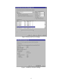
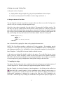
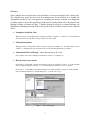
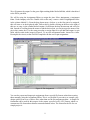
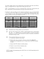
ECE 406 – Spring 2009
Logic Synthesis Tutorial
1. Introduction
The main purpose of this laboratory is to let you become familiar with the Quartus II CAD
system and the Altera Cyclone II FPGA as well as the DE2 board. Its secondary purpose is to
have you starting to design using Verilog. This lab takes a lot longer than lab 1. Make sure to
start early and please read the entire lab before you ask any questions.
2. Learning Objectives
• Learn how to use the basics of the Quartus II CAD system
• Learn how Quartus II can be used to identify common coding problems
• Learn use and port your design to the Altera Cyclone II FPGA.
• Practice the complete design cycle, from specification through programming and
configuring the FPGA.
3. Laboratory Report
You are expected to turn in various documentation as proof that you completed this tutorial. No
formal report is required, but certain items must be turned in as part of your homework
assignment. These items are listed as questions (Q) in this document. Please include each item
in order along with the rest of your homework assignment.
4. Establishing the Correct Environment and Launching Design Analyzer
Open a new terminal window (On the Linux machines, go to System Tools>Terminal)
Create a new directory to run this lab and copy the synthtut.tar file (provided with the tutorial)
into that directory. Next, unpack the file with the following command:
> tar xf synthtut.tar
The purpose of the files within this zipped file are as follows:
1) xorlight.v ->A simple XOR gate used in a design example to illustrate the design flow
using the Quartus II software and the Altera Cyclone II FPGA, and to see actually see
how your design work and LED’s light up!
2) xorlight.csv -> A pin-constraint file to match pins on the Cyclone FPGA to switches and
LEDs on the DE2 evaluation board.
3) count.v ->Used to show how timing issues are dealt with on the Quartus II software.
4) bad.v -> Used to show how the Quartus II software will identify common coding
problems.
Now, let’s set up the Quartus environment with the following commands:
> add quartus71
> quartus &
You should see the Quartus II display appear on the screen (Figure1).
1
Figure 1. The main Quartus II display
5. Starting a new project
Click on File>New Project Wizard. This pops up the ‘New Project Wizard : Introduction’ window.
Click Next. You will see the window shown in Figure 2.
Figure 2. New Project creation
2
The working directory will currently be set to whatever directory you had started Quartus II
from. You may change this if you wish. The project must have a name, which is usually the same
as the top-level design entity that will be included in the project. Choose xorlight as the name for
both the project and the top-level entity, as shown in Figure 2. Click Next. This will take you to
the window in Figure 3.
Figure 3. Adding design files
If you had design files already coded, you would be adding them here (Browse using ‘…’ and the
click Add). Make sure that all your design files are in the working directory. Note: You can
always add design files later too and not necessarily at this step.
We do have xorlight.v as our design file, but we will hold off adding it for now. So do not add
this file as yet and simply click Next. this should take you to the ‘Family and Device Settings’
window show in Figure 4. We have to specify the type of device in which the design will be
implemented. We could let the Quartus II software to select a specific device in the family, but
for now we will specify the device explicitly. Set the Family to “Cyclone II” as shown below,
choose the EP2C35F672C6 device, and click Next. The window that opens up now is the EDA
tools window where the user can specify any third-party tools that should be used. We do not
need any other tools, so leave all the boxes unchecked and click Next. This should take you to the
‘Summary of the Project Settings’ window in Figure 5. Press Finish, which returns to the main
Quartus II window, but with xorlight specified as the new project, in the display title bar.
3
Figure 4 Family and Device Settings
Figure 5. Summary of Project Settings
4
6. Design entry using Verilog Code
At this point we have 2 options:
a) Simply add the design xorlight.v by going to Project>Add/Remove Files in Project
b) Learn to use the Quartus II Text Editor to code a design. (Section 6.1)
6.1 Using the Quartus II Text Editor
You can skip this section if you prefer to use some other text editor to create the Verilog source
code file or if you are simply using the supplied design.
Select File > New, choose Verilog HDL File, and click OK. This opens the Text Editor window. The
first step is to specify a name for the file that will be created. Select File > Save As to open the
pop-up box. In the box labeled Save as type choose Verilog HDL File. In the box labeled File name
type xorlight. Put a checkmark in the box Add file to current project. Click Save, which puts the file
into your working directory and leads to the Text Editor window. Enter the Verilog code
module xorlight (x1, x2, f);
input x1, x2;
output f;
assign f = (x1 & ~x2) | (~x1 & x2);
endmodule
into it. Save the file by typing File > Save, or by typing the shortcut Ctrl-s.
NOTE: The Text Editor provides a collection of Verilog templates. The templates provide
examples of various types of Verilog statements, such as a module declaration, an always block,
and assignment statements. It is worthwhile to browse through the templates by selecting Edit >
Insert Template > Verilog HDL to become familiar with this resource.
At this point your design file should be added to the project. To see the files that are in your
project, go to the ‘Project Navigator’ window on the left top corner of the Quartus II interface
and click on the Files tab and expand the Device Design Files folder. You can also see what files
are on your project by going to Assignments > Settings and clicking on the item Files.
7. Compiling the design
The Quartus II tool analyzes the code, synthesizes the circuit and generates an implementation of
it for the target device. All this is done by the application program called the Compiler.
Run the Compiler by selecting Processing > Start Compilation, or by clicking on the toolbar icon
that looks like a purple triangle. As the compilation moves through various stages, its
progress is reported in a window on the left side of the Quartus II display. Successful (or
unsuccessful) compilation is indicated in a pop-up box that says “Full Compilation was
successful”. Acknowledge it by clicking OK, which leads to the Quartus II display in Figure 6. In
5
the message window, at the bottom of the figure, various messages are displayed. In case of
errors, there will be appropriate messages given.
Figure 6. Display after a successful compilation
At the end of the compilation, a compilation report is produced which is a summary of all the
resources used by the design. This compilation report can also be accessed by selecting
Processing > Compilation Report. The Flow Summary section gives important details about how
many of the FPGA resources have been used. You should notice the following:
• Total logic elements 1 / 33,216 ( < 1% )
• Total registers
0
• Total pins
3 / 475 ( < 1% )
• Total memory bits
0 / 483,850 ( 0% )
Obviously, we haven’t come close to the full capacity of this FPGA, which is good, because this
design is very simple. As our designs grow, we’ll notice that we will get closer and closer to
filling up this FPGA. If our design gets too large, then we’ll need to buy a larger one in order to
implement our design.
6
8. Errors
If the Compiler does not report zero errors, then there is at least one mistake in the Verilog code.
The Compiler may report no errors, but all warnings must also be checked. For example the
‘Incomplete Sensitivity List’ error appears as a warning, but must be corrected even though the
Complier reports a successful compilation. Each error or warning found will be displayed in the
Messages window as shown in Figure 7. Double-clicking on an error or warning message will
highlight the offending statement in the Verilog code in the Text Editor window. Some common
errors
•
Incomplete Sensitivity Lists.
Warning (10235): Verilog HDL Always Construct warning at xorlight.v(7) : variable ‘x2’ is read inside the
Always Construct but isn’t in the Always Construct’s Event Control.
•
Unintentional latches.
Warning (10240): Verilog HDL Always Construct warning at xorlight.v(5) : inferring latch(es) for the
variable “f”, which holds its previous value in one or more paths through the always construct.
•
Unintentional Wired-OR logic. (more than one driver for a net)
Error (10023): Can’t resolve multiple constant drivers for net ”f” at xorlight.v(2)
•
Detects incorrect use of nets.
Error(10219): Verilog HDL Continuous Assignment error at the xorlight.v(5): object “f” on the left-hand
side of assignment must have net type (i.e. ‘f’ more than likely needs to be a ‘wire’ or ‘output’)
Error(10137): Verilog HDL Procedural Assignment error at the xorlight.v(5): object “f” on the left-hand
side of assignment must have a variable data type (i.e. ‘f’ needs to be a ‘reg’)
Figure 7. Error Messages
7
9. Generating a Schematic
Click on Tools > Netlist Viewers > RTL Viewer to get the schematic of the generated circuit. You
can export this schematic to a JPEG or BMP image file by using File > Export for inclusion in
your report.
10. Timing Analyzer Report
A section of the Compilation Report is the Timing Analyzer. This provides information about the
maximum operational frequency of the circuit, critical path etc. On the Compilation Report Click
on the small + symbol next to Timing Analyzer to expand this section of the report, and then
click on the Timing Analyzer item Summary. You should see the following line:
Type
Worst-case tpd
Slack
N/A
Required Time
None
Actual Time
5.246 ns
Here, “tpd” means “point-to-point delay time”, which is the longest possible amount of time
needed for input signals to propagate to the output. Generally, we would want to design a circuit
for a particular speed, and so we would add “timing constraints”, which would give us a
“required-time” and “slack” (which is the required time minus the actual time… a measure of
how close we are to failing our timing constraint).
If this design were to have a clock (as is the case with most designs), then we would see an entry
labeled “Clock Setup” which would give us our theoretical maximum clock frequency for the
design. To see the paths in the circuit that limit the maximum frequency(fmax), click on the
Timing Analyzer item Clock Setup: ’Clock’. This table shows a detailed list of longest paths.
In the absence of timing constraints the Quartus II software implements a designed circuit in a
good but not necessarily the best way in order to keep the compilation time short. If the result
does not meet your expectations, it is possible to specify certain timing constraints that should be
met. Select Assignments > Timing Wizard… to set these constraints. Click “Next” to skip the
introduction, and on the “Project Wide Defaults” screen, for the question “Do you want to
specify an overall default frequency requirement (fmax) for all clocks in this project”, select
“Yes” and click “Next”. In the “Default Frequency (fmax)” screen, enter the desired frequency.
Keep clicking “Next” to accept the defaults for the remaining options, and then click “Finish”.
Now, recompile the circuit. Open the Timing Analyzer Summary to see if the new fmax is
achieved.
11. Pin Assignment
As we noted in section 7 of this tutorial, there are 475 pins on the FPGA, but this does not mean
that we can access all 475 pins on our board. The DE2 board has hardwired connections
between the FPGA pins and the other components on the board. We will use two toggle
switches, labeled SW1 and SW0 on the DE2 board, to provide the external inputs, x1 and x2, to
our example circuit. These switches are connected to the FPGA pins N26 and N25, respectively.
8
We will connect the output f to the green light-emitting diode labeled LEDG0, which is hardwired
to the FPGA pin AE22.
We will be using the Assignment Editor to assign the pins. Select Assignments > Assignment
Editor. Under Category select Pin. Double-click on the entry <<new>> which is highlighted in blue
in the column labeled To. From the drop down menu, click on x1 as the first pin to be assigned:
this will enter x1 in the displayed table. Follow this by double-clicking on the box to the right of
this new x1 entry, in the column labeled Location. Scroll down the drop down menu and select Pin
N26. Instead of scrolling down the menu to find the desired pin, you can just type the name of the
pin in the Location box. Use the same procedure to assign input x2 to pin N25 and output f to pin
AE22, which results in the image in Figure 8. To save the assignments made, choose File > Save.
Recompile the circuit, so that it will be compiled with the correct pin assignments.
Figure 8. Pin Assignment
You can also export and import pin assignments from a special file format, rather than creating
them manually using the Assignment Editor. This is very helpful if you want to re-compile your
design quickly from a set of source files, rather than use the pin-assignment editor. A simple file
format that can be used for this purpose is the comma separated value (CSV) format, which is a
common text file format that contains comma-delimited values. The format for the file for our
simple project is
9
To, Location
x1, PIN_N26
x2, PIN_N25
f, PIN_AE22
By adding lines to the file, any number of pin assignments can be created. Such csv files can be
imported into any design project using Assignments > Import Assignments….
Note that the xorlight.csv file was included in the synthtut.tar file. You can create this file in the
assignment editor by selecting File > Export and clicking on Export. The file xorlight.csv will be
created in the current working directory.
12. Programming and Configuring the FPGA
Plug the supplied 9V DC power supply to the AC power outlet and connect this to the DE2
board. Flip the RUN/PROG switch into the RUN position (JTAG programming mode). Connect
the DE2 board to the computer using the supplied USB cable. Make sure to connect it to the
BLASTER port. Switch on the DE2 board using the red power button. Select Tools > Programmer
to reach the window in Figure 9. If not already chosen by default, select JTAG in the Mode box.
Also, if the USB-Blaster is not chosen by default, press the Hardware Setup... button and select
the USB-Blaster in the window that pops up.
Figure 9. Programming the FPGA
Observe that the configuration file is listed in the window in Figure 9. If the file “xorlight.sof” is
not already listed, then click Add File and select it. This is a binary file produced by the
Compiler’s Assembler module, which contains the data needed to configure the FPGA device.
The extension .sof stands for SRAM Object File. Note also that the device selected is
EP2C35F672, which is the FPGA device used on the DE2 board. Click on the Program/Configure
check box. Now, press Start in the window in Figure 13. When the configuration data has been
downloaded successfully, the LEDs labeled POWER, GOOD, TXD, and RXD should be on.
Try all four valuations of the input variables x1 and x2, by setting the corresponding states of the
switches SW1 and SW0. Verify that the circuit implements an XOR gate.
10
13. Compilation Exercise
Create a new project called counter in a new directory and add the supplied count.v file
(provided as part of the synthtut.tar file). Compile it and answer the questions below.
Q1.
How many logic elements were used in this design?
Q2.
How many flip-flops (registers) are there in this design?
Q3.
Include a copy of the schematic in your write-up. Look at the schematic. Is it what you
expected? How does it differ from the logic specified in the Verilog file?
Q4.
What is the maximum clock-frequency for this design?
14. Debugging Exercise
a) Examine the file bad.v, which was provided as part of the lab2.tar file.
b) Launch Quartus II and try to compile the file.
c) Identify all and fix all potential problems in bad.v. Cut and paste each error message
from the Analysis & Synthesis Messages section of the bad.map.rpt file into your writeup as you find them, along with a description of the error. Otherwise, the bad.map.rpt
file will be overwritten, and you will lose the error messages.
d) Verify that all problems have been removed.
Q5. Please include the following in your write-up:
a) A printout of bad.v with comments identifying the problem statements.
b) A printout of each error message specifying the problems (warnings and errors). This
message should come from the Analysis & Synthesis Messages section of the
bad.map.rpt file, as described above.
c) A printout of a fixed version of bad.v without any problems.
d) A printout of the final Analysis & Synthesis Messages section of the bad.map.rpt
file, showing that there are no problems in the fixed version.
15. Exercise on Design and porting to the FPGA
You will build an N-bit up/down counter and port this design to the FPGA.
Inputs: clock, enable(1-enable counter,0-disable counter), dec (0-count up, 1-count down), reset
(set count value to 0)
Outputs: led_out [4-bit] ( send only the 4 MSB of the count value to the output)
Hook up the ‘enable’ and ‘dec’ inputs to toggle buttons, the ‘reset’ to a push button, use the onboard oscillator as the clock input, and send the 4 bit count value to 4 green LED’s. The clockrate will be too fast for you to actually see the LED’s turn on and off. To circumvent this
problem, you will build an N-bit internal counter which will be driven by the on-board oscillator.
11
You will be sending only the 4 most significant bits of this internal count value to the LEDs as
outputs. You might need to do a couple of runs to find a good value for N.
NOTE: The push-buttons are active-low, meaning that they will be logic 0 when pressed, and
logic 1 when released. This means that the reset in your code must be active-low.
For this lab we will be providing you with a sample pin assignments (to get you started) in Table
1. You may use these if you wish or use your own as long as they are hooked up right. Please
verify in Chapter 4 of the ‘DE2 Development and Education Board: User Manual’ that these
assignments will in fact hook up the design as you need it.
Signal name in your
design
clock
enable
dec
reset
led_out[3]
led_out[2]
led_out[1]
led_out[0]
Signal Name
FPGA pin no.
CLOCK_50
PIN_N2
SW0
PIN_N25
SW1
PIN_N26
KEY0
PIN_G26
LEDG3
PIN_V18
LEDG2
PIN_W19
LEDG1
PIN_AF22
LEDG0
PIN_AE22
Table 1 : Pin Assignments
Description
On-Board Clock
Toggle Switch[0]
Toggle Switch[1]
PushButton[0]
LED Green[3]
LED Green[2]
LED Green[1]
LED Green[0]
Q6.
Demonstrate your working module to your lab instructor.
Q7.
How fast is the on-board clock? Include a rough calculation of how you determined
this value. It is suggested that you count the number of times the led_out[3]
transitions in a second. Use this to determine the number of transitions of the MSB of
the internal count per second.
Q8.
Please include the following in your write-up:
a) A hand-drawn schematic of your design
b) Printout of the Analysis & Synthesis Messages section of the .map.rpt file,
showing that your design had no errors. You must remove all the errors and bad
warnings.
c) Printout of the RTL schematic created by Quartus.
d) Printouts of your test fixture simulation results.
e) Explanation of your test strategy
NOTE: Use the JTAG programming mode and NOT the Active Serial Programming mode to
program the FPGA.
12
We have now covered all the CAD tools that you will be using in this class.
Revision History
August, 2002 : Rewritten from previous versions (P. Franzon)
February, 2003: Updated (J. Abell)
June, 2003: Updated (A. Woodson)
September, 2003: Updated (A. Woodson)
February, 2006: Updated to 180nm IIT-SOC Standard-Cell Library (R. Davis)
October, 2006: Updated to Quartus software and Altera DE2 board (U. Pazhayaveetil)
13