1
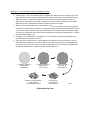
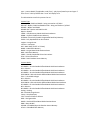
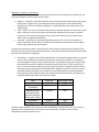
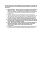
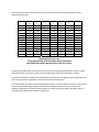
MEMS Cost and Price Model User Manual IC Knowledge LLC, PO Box 20, Georgetown, MA 01833 Tx: (978) 352 – 7610, Fx: (978) 352 – 3870, email: [email protected] Version 2015 model Introduction This manual presents an overview of MEMS Cost and Price Model and the basic workings of the model. Model description The MEMS Cost and Price Model is designed to easily calculate the manufacturing cost and selling price of most MEMS products. The model support up to 2 MEMS die and up to 2 IC die per product. The IC process support is limited to processes that are typically included in MEMS products and the MEMS model is not a general usage IC Cost and Price calculator. For IC Cost and Price calculations we recommend our IC Cost and Price Model. Please note that our cost models are cost of goods sold (COGS) models and do not include below the line costs such as research and development (R&D) or selling, general and administration costs (SG&A). Our pricing calculations are cost plus gross margin (GM). R&D and SG&A costs are absorbed in GM as well as profits. Support and updates As a licensee to the MEMS Cost and Price Model you will receive all updates made to the model for twelve months from the date of purchase emailed to your email address of record. If you change your email address it is your responsibility to notify us. Free phone and email support will be provided for twelve months from the date of purchase of the model. On‐site or other forms of support are not provided. Model conventions There are several conventions used throughput the model. The gray areas on each model sheet contain the model inputs and outputs. The inputs that can be directly changed by the user are white areas within the gray areas; the gray areas contain labels and model driven outputs and cannot be directly changed by the user. Throughout the model there are red dots indicating comments. Moving the cursor over the red dots displays information explaining input or outputs. In this manual, regular, bold and underlined text describe the model and model features. Italic text provides background on the inner workings of the model. Tab color coding All IC Knowledge Models follow the same worksheet tab color coding scheme. Tab Color Grey Sheet Type Information Red Brown Blue Purple Main model wide selections Model outputs Process details and control Equipment and Facilities Green Materials Examples License, Revisions, HELP, Price, Revision History Main Selection Cost Summary, Cost Per Step Custom MEMS Process Custom MEMS Fab, Custom MEMS Equipment Custom MEMS Materials Worksheet overview The following is a brief description of the model worksheets and the purpose of each sheet. The sheet tabs are color coded, gray is informational (these sheets may in some cases be editable but do not drive the model results), red are the main drivers (these sheets are editable), brown are results (these sheets are not editable), blue modifies the processes or performs comparisons or calculations (these sheets are editable). License (gray tab) – the model software license. This sheet is not editable. Introduction (gray tab) – a brief introduction to IC Knowledge and our cost modeling product line as well as disclaimer and warrantee information. This sheet is not editable. HELP (gray tab) – a listing of the various ways to get help with the model. This sheet is not editable. Main Selections (red tab) – this si the sheet where the main selections for the model are made.. This sheet is user editable. Defaults (red tab) – this sheet displays the default values for all of the model defaults and allows the user to override them. This sheet is user editable. Cost Summary (brown tab) – the main summary of the cost model results including wafer, test and packaging cost. This sheet is not user editable. Cost Per Step (brown tab) – displays the cost per step for the main step types used in the MEMS processes. This sheet is not user editable. Price (gray tab) – sheet to help with selling price estimation. This sheet is user editable. Custom MEMS Process (blue tab) – a sheet to allow custom processes to be defined to run the MEMS die 1 and or MEMS die 2. This sheet is used editable. Custom MEMS Fab (purple tab) – a sheet to allow custom fabs to be defined to run the MEMS die 1 and or MEMS die 2 processes. This sheet is used editable. Custom MEMS Equipment (purple tab) – a sheet to allow custom equipment to be defined to run the MEMS die 1 and or MEMS die 2 processes. This sheet is used editable. Custom MEMS Materials (green tab) – a sheet to allow custom materials to be defined to be used in the MEMS die 1 and or MEMS die 2 processes. This sheet is used editable. Revision History (gray tab) – a history of changes made to the current year model. This sheet is not user editable. Detailed worksheet descriptions In this section the “active” worksheets are described in more detail. Worksheet such as ‘License’, ‘Introduction’, ‘Help’, ‘Revision History’, ‘Lists’ and the blank worksheets are expected to be self‐ explanatory. Background – The IC Manufacturing Flow (MEMS is similar) The following are the main steps in the IC manufacturing flow: Starting wafer – this is purchased by all IC manufacturers. Wafers come in a variety of sizes and types. When you select a process the appropriate wafer size and type is automatically selected. Wafer fabrication – anywhere between tens to tens of thousands of integrated circuits are fabricated on the surface of the wafer. The wafer yield is the number of wafers that complete fabrication process divided by the number of wafers started into the fab. Wafer sort (also called wafer test or wafer probe) – the ICs on the wafer surface are tested and the bad ICs are mark with an ink dot or in an electronic map so they won’t be packaged. Die yield is the number of die that pass wafer sort divided by the total number of die on the wafer. Wafer sort may be a single pass test or may include multiple passes at different temperatures, or before and after bakes and burn‐ins. Packaging – the individual ICs on the wafer are cut up and put into protective packages that provide electrical connections to the IC. Class test (also called final test) – the packaged ICs are tested to insure the ICs were correctly packaged without damage. For some ICs they can’t be fully tested until they are packaged and this may be the first full test. Class test may be a single pass test or may include multiple passes at different temperatures, or before and after bakes and burn‐ins. 1) Starting substrate silicon wafer (purchased). 2) Wafer fabrication fabricate IC’s on the wafer 4) Packaging assemble IC’s into packages 5) Mark & class/final test mark and final test packaged product IC Manufacturing Flow 3) Wafer sort/test test each IC, mark bad IC’s 14003 Main Selections (red tab) This is the main sheet driving the model. Year to model ‐ At the top of the sheet in row 7 is the year to model, 2000 to 2020 are supported. You should select the year the product was manufactured. The year effects labor and utility costs, depreciation and die yields. Select the product to model – in row 9 there is a drop down of predefined MEMS products. If the product you wish to model is in the drop down list and all settings throughout the model are set to default, as soon as you select a product here you have a complete model. You can also override the product specific defaults throughout the model. If you select “User defined” here you must define the product in the other areas on this sheet. MEMS Die 1 – starting at row 11 the first MEMS die is defined (if applicable). The MEMS model allows for up to 2 MEMS die and up to 2 IC die in each product. o MEMS Die 1 Process (default) – displays the default process used to produce the first MEMS die if applicable. The nomenclature is company (if applicable) – process – process details (optional). If there is no MEMS 1 die by default then “none” will display here. o MEMS Die 1 Process (selected) ‐ if “default” is selected here the default process from the cell above will be used or you can override the default by selecting a process here. The process nomenclature is the same as the cell above. If you select “Enter steps” here you must define a process on the ‘Custom MEMS Process’ sheet. o Messages – if you select ‘Enter steps’ above a message will display reminding you to enter the steps on the ‘Custom MEMS Process’ sheet. o MEMS Process 1 Fab (default) – displays the default Fab used to run the MEMS die 1 process, if applicable. The nomenclature is company – fab location/name. o MEMS Process 1 Fab (selected) – if “default” is selected here, then the default fab displayed above will be used for the MEMS die 1 fab. You can also override the fab and pick any of the pre‐defined fabs. The model does not filter processes and fabs so you can select any MEMS fab to run any MEMS process. If you select “User entered” you must define a fab yourself on the ‘Custom MEMS Fab’ sheet. o Messages – if you select ‘User entered’ above a message will display reminding you to define a fab on the ‘Custom MEMS Fab’ sheet. o MEMS Foundry Margin (default) ‐ if the company making the MEMS product uses a foundry for MEMS die 1 fabrication the default foundry margin will display here. If the company making the MEMS product uses their own fab for the MEMS die 1 process, the default foundry margin will be 0%. Also if you selected “User defined” for the product the default foundry margin will be zero. o MEMS Foundry Margin (selected) – if “Default” is selected the default foundry margin displayed above will be used or you can override the default margin and select your own here. o MEMS Die 1 Size (default) – for predefined products selected in row 9 a default die size will be displayed here for the MEMS die 1 if applicable. There are independent entries for die length and width. o MEMS Die 1 Size (user entry) – you can enter your own MEMS die 1 – die size here but the entered value will not be used unless select “User entry” in the cells below. There are independent entries for die length and width. o MEMS Die 1 Size Source – if “Default” is selected then the default die size is used, if “User entered” is selected the user entered die size is used. There are independent entries for die length and width and each one is individually controlled. The model assumes physical die size and a 2 millimeter edge exclusion. Die Size o o Starting wafer 1 (default) – the default first wafer type for the MEMS die 1 (if applicable) is displayed. For each MEMS die up to 3 starting wafers are supported and this is the first of 3 wafers. Starting wafer 1 (selected) – if “Default” is selected here the default wafer 1 displayed above is used or you can select a wafer type from the dropdown. The dropdown selections. GaAs – gallium arsenide Ge ‐ germanium Glass – Etched ‐ glass substrates that have been etched Glass ‐ Ultrasonic drilled ‐ glass substrates that have been ultrasonic drilled LiNbO3 – lithium niobate substrates Nafion – nafion substrates (a fluoropolymer subtsrate) Pyrex – pyrex glass substrates Quartz – quartz glass substrates Si ‐ 1 side polished – single side polished silicon wafers Si ‐ 2 side polished – double side polished silicon wafers Si – Epi – silicon wafer with an epitaxial layer on it Si – SOI – silicon on insulator wafer o o o Starting wafer 2 (default) – the default second wafer type for the MEMS die 2 (if applicable) is displayed. For each MEMS die up to 3 starting wafers are supported and this is the second of 3 wafers. Starting wafer 2 (selected) – if “Default” is selected here the default wafer 2 displayed above is used or you can select a wafer type from the dropdown. Starting wafer 3 (default) – the default third wafer type for the MEMS die 2 (if applicable) is displayed. For each MEMS die up to 3 starting wafers are supported and this is the third of 3 wafers. o o o o o o o Starting wafer 3 (selected) – if “Default” is selected here the default wafer 3 displayed above is used or you can select a wafer type from the dropdown. Gross die (default) – the model calculated gross whole die based on the default or user entered die size from above. Gross die (user entry) – a user entered value for gross whole die. This number does not do anything unless ‘Gross die (select)” down below this cell is set to “User entry”. Gross die (select) – if “Default” is selected here the default gross die value is used, if “user entry” is selected the user entered gross die value is used. Die yield (default) – the model default die yield is displayed here. For predefined products a default die yield is displayed that is product specific. Die yield (user entry) – a user entered value for die yield. This number does not do anything unless ‘Die yield (select)” down below this cell is set to “User entry”. Die yield (select) – if “Default” is selected here the default die yield value is used, if “user entry” is selected the user entered gross die yield is used. There are also several different scenarios around process and design maturity listed here as options that fill in die yields based on those selections. MEMS Die 2 – starting at row 36 the second MEMS die is defined (if applicable). The MEMS model allows for up to 2 MEMS die and up to 2 IC die in each product. o MEMS Die 2 Process (default) – displays the default process used to produce the first MEMS die if applicable. The nomenclature is company (if applicable) – process – process details (optional). If there is no MEMS 2 die by default then “none” will display here. o MEMS Die 2 Process (selected) ‐ if “default” is selected here the default process from the cell above will be used or you can override the default by selecting a process here. The process nomenclature is the same as the cell above. If you select “Enter steps” here you must define a process on the ‘Custom MEMS Process’ sheet. o Messages – if you select ‘Enter steps’ above a message will display reminding you to enter the steps on the ‘Custom MEMS Process’ sheet. o MEMS Process 2 Fab (default) – displays the default Fab used to run the MEMS die 2 process, if applicable. The nomenclature is company – fab location/name. o MEMS Process 2 Fab (selected) – if “default” is selected here, then the default fab displayed above will be used for the MEMS die 2 fab. You can also override the fab and pick any of the pre‐defined fabs. The model does not filter processes and fabs so you can select any MEMS fab to run any MEMS process. If you select “User entered” you must define a fab yourself on the ‘Custom MEMS Fab’ sheet. o Messages – if you select ‘User entered’ above a message will display reminding you to define a fab on the ‘Custom MEMS Fab’ sheet. o MEMS Foundry Margin (default) ‐ if the company making the MEMS product uses a foundry for MEMS die 2 fabrication the default foundry margin will display here. If the company making the MEMS product uses their own fab for the MEMS die 2 process, the default foundry margin will be 0%. Also if you selected “User defined” for the product the default foundry margin will be zero. o MEMS Foundry Margin (selected) – if “Default” is selected the default foundry margin displayed above will be used or you can override the default margin and select your own here. o o o o o o o o o o o o o o o MEMS Die 2 Size (default) – for predefined products selected in row 9 a default die size will be displayed here for the MEMS die 2 if applicable. There are independent entries for die length and width. MEMS Die 2 Size (user entry) – you can enter your own MEMS die 2 – die size here but the entered value will not be used unless select “User entry” in the cells below. There are independent entries for die length and width. MEMS Die 2 Size Source – if “Default” is selected then the default die size is used, if “User entered” is selected the user entered die size is used. There are independent entries for die length and width and each one is individually controlled. Starting wafer 1 (default) – the default first wafer type for the MEMS die 2 (if applicable) is displayed. For each MEMS die up to 3 starting wafers are supported and this is the first of 3 wafers. Starting wafer 1 (selected) – if “Default” is selected here the default wafer 1 displayed above is used or you can select a wafer type from the dropdown. The dropdown selections. Starting wafer 2 (default) – the default second wafer type for the MEMS die 2 (if applicable) is displayed. For each MEMS die up to 3 starting wafers are supported and this is the second of 3 wafers. Starting wafer 2 (selected) – if “Default” is selected here the default wafer 2 displayed above is used or you can select a wafer type from the dropdown. Starting wafer 3 (default) – the default third wafer type for the MEMS die 2 (if applicable) is displayed. For each MEMS die up to 3 starting wafers are supported and this is the third of 3 wafers. Starting wafer 3 (selected) – if “Default” is selected here the default wafer 3 displayed above is used or you can select a wafer type from the dropdown. Gross die (default) – the model calculated gross whole die based on the default or user entered die size from above. Gross die (user entry) – a user entered value for gross whole die. This number does not do anything unless ‘Gross die (select)” down below this cell is set to “User entry”. Gross die (select) – if “Default” is selected here the default gross die value is used, if “user entry” is selected the user entered gross die value is used. Die yield (default) – the model default die yield is displayed here. For predefined products a default die yield is displayed that is product specific. Die yield (user entry) – a user entered value for die yield. This number does not do anything unless ‘Die yield (select)” down below this cell is set to “User entry”. Die yield (select) – if “Default” is selected here the default die yield value is used, if “user entry” is selected the user entered gross die yield is used. There are also several different scenarios around process and design maturity listed here as options that fill in die yields based on those selections. IC Die 1 – starting at row 61 the first IC die is defined (if applicable). The MEMS model allows for up to 2 MEMS die and up to 2 IC die in each product. For some products the IC process includes creating of the MEMS structures on top of the IC die and this is where those processes are selected. o IC Die 1 Process (default) – displays the IC process used to make the first IC die (if applicable). The nomenclature is wafer size – node – company (if foundry is diaplyed here it is a generic foundry process) – process name (if applicable or NA if not) – process type – process details (if applicable or NA if not) – poly layers/metal layers and type. If there is no IC 1 die by default then “none” will display here. The abbreviations used in the process list are: Process Type BCD = Bipolar, CMOS and DMOS – being removed on 1/1/2016 BCD SOI = Bipolar, CMOS and DMOS on SOI – being removed on 1/1/2016 BiCMOS = Bipolar and CMOS BiCMOS SOI = Bipolar and CMOS on SOI Bipolar = Bipolar CMOS = Complimentary Metal Oxide Semiconductor DRAM = Dynamic Randon Access Memory EEPROM = Electrically Erasable Programable Read Only Memory FDSOI = Fully Depelted Silicon On Insulator ImgSen = Image Sensor InterPos = Interposer MG = Multi‐Gate (FinFET or TriGate) NAND = NAND Flash Memory NMOS = N type Metal Oxide Semiconductor NOR = NOR Flash Memory PDSOI = Partially Depeleted Silicon On Insulator SiGe = Silicon Germanium SRAM = Static Random Access Memory Process details 100V = 100 volts 20V DMOS = 20 volts Double Diffused Metal Oxide Semiconductor 30V = 30 volts 30V DMOS = 30 volts Double Diffused Metal Oxide Semiconductor 40V DMOS = 40 volts Double Diffused Metal Oxide Semiconductor 500V DMOS = 500 volts Double Diffused Metal Oxide Semiconductor 5Vts = 5 threshold voltages 60V = 60 volts 60V DMOS = 60 volts Double Diffused Metal Oxide Semiconductor 650V DMOS = 650 volts Double Diffused Metal Oxide Semiconductor 65V DMOS = 65 volts Double Diffused Metal Oxide Semiconductor 80V = 80 volts 80V DMOS = 80 volts Double Diffused Metal Oxide Semiconductor Analog = Analog BSI = Backside Image Sensor Comp = Complimemtary CPA = Common Platform Alliance DGO = Dual gate oxide DMOS = Double Diffused Metal Oxide Semiconductor DNW = Deep N‐Well eDRAM = Embedded Dynamic Random Access Memory eFlash = Embedded Flash Memory o o o o o o FPGA = Field Programable Gate Array FSI = Front Side Illuminated Image Sensor Fuse = Fuse Ge PMOS = Germanium P Type Metal Oxide Semiconductor HfO/AlO = Hafnium Oxide/Aluminum Oxide High‐K Dielectric HKMG = High‐k metal gate HKMIM = High‐K Metal ‐Insulator‐Metal Capacitor HV = High Voltage LV = Low Voltage MIM = Metal‐Insulator‐Metal Capacitor Mixed Sig = Mixed Signal NMOS = N Type Metal Oxide Semiconductor PMOS = P Type Metal Oxide Semiconductor PPCaps = Polysiliocn to Polysilicon capacitors Pressure Sensor = Pressure Sensor RCAT = Recessed Access Array Transistor RDL = Redistribution Layer RF = Radio Frequency Saddle Fin = Saddle FinFET Acccess Array Transistor Schottky = Schotty diode Schottky, TFR = Thin Film resistor SiGe = Silicon Germanium Silk ILD = A Low‐K Spin‐On Interlevel Dielectric TaN Res = Tantulum Nitirde Resistor TGO = Triple Gate Oxide VNPN = Vertical P‐Type/N‐Type/P‐Type Bipolar Transistor ZAZ = Zirconium Oxide/Aluminum Oxide/Zirconium Oxide High‐K Dielectric IC Die 1 Process (selected) ‐ if “default” is selected here the default process from the cell above will be used or you can override the default by selecting a process here. The process nomenclature is the same as the cell above. IC Foundry Margin (default) ‐ if the company making the MEMS product uses a foundry for IC die 1 fabrication the default foundry margin will display here. If the company making the MEMS product uses their own fab for the IC die 1 process, the default foundry margin will be 0%. Also if you selected “User defined” for the product the default foundry margin will be zero. IC Foundry Margin (selected) – if “Default” is selected the default foundry margin displayed above will be used or you can override the default margin and select your own margin here. IC Die 1 Size (default) – for predefined products selected in row 9 a default die size will be displayed here for the IC die 1 if applicable. There are independent entries for die length and width. IC Die 1 Size (user entry) – you can enter your own IC die 1 – die size here but the entered value will not be used unless select “User entry” in the cells below. There are independent entries for die length and width. IC Die 1 Size Source – if “Default” is selected then the default die size is used, if “User entered” is selected the user entered die size is used. There are independent entries for die length and width and each one is individually controlled. Gross die (default) – the model calculated gross whole die based on the default or user entered die size from above. o Gross die (user entry) – a user entered value for gross whole die. This number does not do anything unless ‘Gross die (select)” down below this cell is set to “User entry”. o Gross die (select) – if “Default” is selected here the default gross die value is used, if “user entry” is selected the user entered gross die value is used. o Die yield (default) – the model default die yield is displayed here. For predefined products a default die yield is displayed that is product specific. o Die yield (user entry) – a user entered value for die yield. This number does not do anything unless ‘Die yield (select)” down below this cell is set to “User entry”. o Die yield (select) – if “Default” is selected here the default die yield value is used, if “user entry” is selected the user entered gross die yield is used. There are also several different scenarios around process and design maturity listed here as options that fill in die yields based on those selections. IC Die 2 – starting at row 76 the first IC die is defined (if applicable). The MEMS model allows for up to 2 MEMS die and up to 2 IC die in each product. For some products the IC process includes creating of the MEMS structures on top of the IC die and this is where those processes are selected. o IC Die 2 Process (default) – displays the IC process used to make the first IC die (if applicable). The nomenclature is wafer size – node – company (if foundry is displayed here it is a generic foundry process) – process name (if applicable or NA if not) – process type – process details (if applicable or NA if not) – poly layers/metal layers and type. If there is no IC 1 die by default then “none” will display here. o IC Die 2 Process (selected) ‐ if “default” is selected here the default process from the cell above will be used or you can override the default by selecting a process here. The process nomenclature is the same as the cell above. o IC Foundry Margin (default) ‐ if the company making the MEMS product uses a foundry for IC die 2 fabrication the default foundry margin will display here. If the company making the MEMS product uses their own fab for the IC die 2 process, the default foundry margin will be 0%. Also if you selected “User defined” for the product the default foundry margin will be zero. o IC Foundry Margin (selected) – if “Default” is selected the default foundry margin displayed above will be used or you can override the default margin and select your own margin here. o IC Die 2 Size (default) – for predefined products selected in row 9 a default die size will be displayed here for the IC die 1 if applicable. There are independent entries for die length and width. o IC Die 2 Size (user entry) – you can enter your own IC die 1 – die size here but the entered value will not be used unless select “User entry” in the cells below. There are independent entries for die length and width. o IC Die 2 Size Source – if “Default” is selected then the default die size is used, if “User entered” is selected the user entered die size is used. There are independent entries for die length and width and each one is individually controlled. o Gross die (default) – the model calculated gross whole die based on the default or user entered die size from above. o Gross die (user entry) – a user entered value for gross whole die. This number does not do anything unless ‘Gross die (select)” down below this cell is set to “User entry”. o o o o o Gross die (select) – if “Default” is selected here the default gross die value is used, if “user entry” is selected the user entered gross die value is used. Die yield (default) – the model default die yield is displayed here. For predefined products a default die yield is displayed that is product specific. Die yield (user entry) – a user entered value for die yield. This number does not do anything unless ‘Die yield (select)” down below this cell is set to “User entry”. Die yield (select) – if “Default” is selected here the default die yield value is used, if “user entry” is selected the user entered gross die yield is used. There are also several different scenarios around process and design maturity listed here as options that fill in die yields based on those selections. Test – this section defines the tests for the product. There are multiple levels of test, each of 2 MEMS die (if applicable) and each of 2 IC die if applicable are wafer sorted (also known as wafer probe) and then the entire product is class tested (also known as final test). o MEMS Die 1 Sort (default) – if a pre‐defined product is selected in row 9 and if a MEMS die 1 is used then the default wafer sort test is displayed here. o MEMS Die 1 Sort (select) – if “default” is selected here then the default MEMS die test displayed above is used or you can select your own MEMS die 1 test. For “user defined” products (row 9) you must select your own test here (if applicable). o MEMS Die 2 Sort (default) – if a pre‐defined product is selected in row 9 and if a MEMS die 2 is used then the default wafer sort test is displayed here. o MEMS Die 2 Sort (select) – if “default” is selected here then the default MEMS die test displayed above is used or you can select your own MEMS die 2 test. For “user defined” products (row 9) you must select your own test here (if applicable). o IC Die 1 Sort (default) – if a pre‐defined product is selected in row 9 and if an IC die 1 is used then the default wafer sort test is displayed here. o IC Die 1 Sort (select) – if “default” is selected here then the default IC 1 die test displayed above is used or you can select your own IC die 1 test. For “user defined” products (row 9) you must select your own test here (if applicable). o IC Die 2 Sort (default) – if a pre‐defined product is selected in row 9 and if an IC die 2 is used then the default wafer sort test is displayed here. o IC Die 2 Sort (select) – if “default” is selected here then the default IC die 2 test displayed above is used or you can select your own IC die 2 test. For “user defined” products (row 9) you must select your own test here (if applicable). o Class Test (default) – if a pre‐defined product is selected in row 9 then the default class test displays here. o Class Test (select) – if “default” is selected here then the default value from the row above is used or you can select a class test type here overriding the row above. For “user defined” products (row 9) you must select your own test here. Packaging – this section defines the MEMS product package. o Package (default) – if a pre‐defined product is selected in row 9 then a default MEMS product package is displayed here. o Package (selected) – if “default” is selected here then the default package type from the row above is used or you can select your own package here. For “user defined” products (row 9) you must select your own package here. Foundry volumes and margin There are basically three kinds of companies in the semiconductor (or MEMS) business: Integrated Device Manufacturer (IDM) – IDM’s design their own products, fabricate the wafers, test them, package the parts, test them again and take them to market. Fabless – fabless companies design semiconductors but rely on other companies to fabricate the parts for them. They may or may not test the parts themselves and they typically outsource the packaging as well. Foundry – a company that owns their own wafer fabs and fabricates wafers for others. If the process you select is an IDM process (the company in the process description is an IDM) then the foundry margin will be zero. This is because the company transfers the fabricated wafers internally and only takes a margin at the end when the finished part is sold. If you select a foundry process (the company in the process is a foundry) then the foundry will sell the wafers to the fabless semiconductor company with a margin added to it (some IDMs also buy at least part of their wafer requirement from foundries). The cost to make a wafer depends on the process, the wafer fab and how full the fab is. Unless a customer is so big that they largely determine how full a fab is the wafer cost is not sensitive to the customer volume, however, the margin is very sensitive to volume. Background – Cost Accounting Cost accounting practices break out manufacturing costs in three categories: 1. Material – material only includes materials that become part of the final product that is shipped. Materials consumed in product are included in overhead and do not count as materials. 2. Labor – labor only include direct or “touch” labor, basically the operators who make the product. Indirect labor such as engineers, technicians, managers and supervisors are included in overhead. 3. Overhead – everything else. The following table summarizes what is included in each category for different phases of IC production. Category Wafer Fabrication Packaging Test Material Starting Wafer Substrates, Leadframes, None Wire, Mold Compound Labor Operators Operators Operators Depreciation, Depreciation, Overhead Depreciation, Equipment Equipment Equipment maintenance, Indirect maintenance, Indirect maintenance, Indirect labor, Facilities costs, labor, Facilities costs, labor, Monitor wafers, Consumables Consumables Facilities costs, Consumables Background ‐ Wafer Cost Calculation As previously described, cost accounting practices break up the cost to manufacture a product for sale into three categories, material, labor and overhead: Material – material is confined to materials used to make the product that becomes part of the product that is shipped. Only if the material becomes a physical part of the product being shipped does it count in the material category. For wafer fabrication the only material is the starting wafer. Labor – labor in this case is restricted to direct labor sometimes referred to as touch labor. Direct labor is the labor cost for the operators who physically manufacture the product. Engineers, supervisors, technicians and managers do not count as direct labor and are included in the indirect labor category described below. Overhead – everything else required manufacturing the product. In the IC Knowledge cost models overhead is broken down into depreciation, equipment maintenance, monitor wafers, indirect labor, facilities and consumables. As previously described overhead is everything other than material (starting wafers) and labor (direct labor from operators) required to produce the product. The following is a further breakout and discussion of the various overhead sub categories: Depreciation – equipment has a finite usable lifetime. The idea behind depreciation is to take the cost of a piece of equipment and write it off over the course of its useful life. For example if a piece of equipment costs one million dollar and has a useful lifetime of five years, two hundred thousand dollars would be charged to manufacturing cost each year for each of the first five years. In the semiconductor industry the useful life of some process equipment may be shorter than government regulations allow and furthermore regulations vary from country to country. Generally speaking the industry has settled on five year depreciation for process equipment when reporting results (although other rules may be used for tax purposes). The following are the default depreciation rates used in the cost models: Item Process tools Process tools installation Building systems (ultrapure water, gas and chemicals, cleanroom, HVAC) Automation Building structure Useful life 5 years 5 years Depreciation rate 20% 20% 10 years 10% 10 years 15 years 10% 7% The deprecation calculation is the cost of the item multiplied by the depreciation rate. This amount is charged to the manufacturing cost each year until the useful life is reached at which time the depreciation for that items goes to zero. With expansions and upgrades there may be a wide variety of equipment ages in the same facility. The Cost Model provides for an initial equipment set and up to three upgrades/expansions and tracks each set individually. Equipment Maintenance – the cost of parts and service contracts for the process equipment are captured in this category. The company employees such as technicians and engineers that maintain the equipment are not counted in this category. Equipment maintenance is calculated as a percentage of the original acquisition cost of the equipment used to estimate yearly maintenance costs. Indirect labor – engineers (both process and equipment), technicians (both process and equipment), supervisors and managers are all counted in this category. Indirect labor hour per mask layer are used to estimate total indirect labor hours. Total indirect labor hour are then broken down by type using “typical” fab indirect labor profiles and labor rates for engineers, technicians, supervisors and managers by country are used to calculate indirect labor costs. Monitor wafers – test wafers used to monitor the performance of equipment. These wafers are used to perform a test by running them through one or more process steps and then measuring the result. The wafers are then scrapped or reclaimed. Facilities – the cost of utilities (electricity, natural gas and water), ultrapure water generation, waste water treatment, facility maintenance (HVAC, Ultrapure water, gas and chemical systems), insurance, occupancy (cleaning and waste disposal), landscaping and telecommunications. Consumables – reticles, photochemicals, cleaning chemicals, etching and deposition gases, bulk gases, CMP pads and slurries, sputter targets, implant sources, deposition precursors, etc. Background – Wafer fab equipment depreciation Please not this discussion is from our IC Model, the MEMS model currently supports 3 upgrades for IC fabs but will be transitioning to 10 upgrades over the next year to match the IC model. Due to the complexity of the wafer fab equipment calculations they bear a more detailed examination. The model allows a fab to have an initial equipment set and up to 10 upgrades. In each case when and what came online and how much it cost is tracked. The model also allows the user to adjust the depreciation period. In the simplest example a wafer fab is built with an initial equipment set and is never upgraded. If for example a one billion dollar equipment set is put online, then by default $200 million dollars will be written off each of the first 5 years and in year 6 depreciation becomes zero. If a user were to change the depreciation to 7 years, then $143 million dollars would be written off each of the first 7 years and then go to 0 in year 8. If a fab is less than 6 years, old the depreciation be default would be 20% per year, if you switch from 5 year to 7 year depreciation the depreciation would switch to ~14% decreasing the depreciation charges. If however the fab is 6 years old the depreciation would be 0 by default and if you switched to 7 year depreciation the depreciation would become ~14% increasing the depreciation cost. Once a sufficient amount of time has passed changing the length of depreciation has no effect because the equipment is fully depreciated in all cases. If the fab has gone through multiple upgrades the situation gets a lot more complicated. For example, if a fab had an initial equipment set of $1 billion dollars and then each year had a $100 million dollar equipment upgrade for the first 5 years the deprecation would look like the following. Initial Upgrade Upgrade Upgrade Upgrade Upgrade Total set 1 2 3 4 5 Year 1 $200M $0M $0M $0M $0M $0M $200M Year 2 $200M $20M $0M $0M $0M $0M $220M Year 3 $200M $20M $20M $0M $0M $0M $240M Year 4 $200M $20M $20M $20M $0M $0M $260M Year 5 $200M $20M $20M $20M $20M $0M $280M Year 6 $0M $20M $20M $20M $20M $20M $100M Year 7 $0M $0M $20M $20M $20M $20M $80M Year 8 $0M $0M $0M $20M $20M $20M $60M Year 9 $0M $0M $0M $0M $20M $20M $40M Year 10 $0M $0M $0M $0M $0M $20M $20M Year 11 $0M $0M $0M $0M $0M $0M $0M Year 12 $0M $0M $0M $0M $0M $0M $0M Year 13 $0M $0M $0M $0M $0M $0M $0M Depreciation Versus Year. 5 Year depreciation, $1 billion dollar initial investment and $100 million dollar upgrade each of the first 5 years. The next table illustrates the depreciation for the same case except that the depreciation period is changed to seven years. Initial Upgrade Upgrade Upgrade Upgrade Upgrade Total set 1 2 3 4 5 Year 1 $143M $0M $0M $0M $0M $0M $143M Year 2 $143M $14M $0M $0M $0M $0M $157M Year 3 $143M $14M $14M $0M $0M $0M $171M Year 4 $143M $14M $14M $14M $0M $0M $186M Year 5 $143M $14M $14M $14M $14M $0M $200M Year 6 $143M $14M $14M $14M $14M $14M $214M Year 7 $143M $14M $14M $14M $14M $14M $214M Year 8 $0M $14M $14M $14M $14M $14M $71M Year 9 $0M $0M $14M $14M $14M $14M $57M Year 10 $0M $0M $0M $14M $14M $14M $43M Year 11 $0M $0M $0M $0M $14M $14M $29M Year 12 $0M $0M $0M $0M $0M $14M $14M Year 13 $0M $0M $0M $0M $0M $0M $0M Depreciation Versus Year. 7 Year depreciation, $1 billion dollar initial investment and $100 million dollar upgrade each of the first 5 years. Comparing the tables we can see that for the first five years the five year depreciation results in higher total depreciation costs, then for years seven through twelve seven year depreciation is higher. In reality the situation is actually more complex than this with up to ten upgrades plus as upgrades take place some of the older equipment is removed and must be accounted for. The model handles all of this accounting automatically and it isn’t even visible to the user. If you feel you need to see the details of the equipment calculations and depreciation you need to purchase our strategic model where all of the calculation details are visible. We do not expose that detail in the IC model due to the audience the model is designed for. Cost Summary (brown tab) The cost summary sheet summarizes all of the cost results from the model. This page is not user editable. General information Rows 7 and 8 display information general information on the year being modeled and the product selected. Rows 10 through 40 break out the wafer fabrication and die costs for each of the 4 possible die in a product. Column D has the MEMS die 1 (if applicable), column E has the MEMS die 2 (if applicable), column F has the IC ide 1 (if applicable) and column G has the IC die 2 (if applicable). Wafer fab Rows 11 through 16 presents the wafer fab country, wafer size, wafer fab capacity in wafers per month), the year the wafer fab was built and the wafer fab equipment depreciation rate for the fabs used for each die type. Wafer cost Rows 17 through 28 break out the wafer costs by category for each die type. The costs are broken down into starting wafer, direct labor, depreciation, equipment maintenance, indirect labor, monitor wafers, facilities and consumables, wafer cost (total of the previous 8 items), wafer yield (wafers out of the fab divided by wafers into the fab) and finally the yielded wafer cost (wafer cost divided by wafer yield). The numbers are all dollars per wafer. Foundry margin Rows 29 through 32 present the foundry margin (%), foundry margin ($/wafer) and wafer cost with foundry margin (wafer cost plus foundry margin) for each of the four die types. Sort cost Rows 34 and 35 present the wafer sorts cost and wafer cost with sort cost for the four die types (wafer cost with foundry margin plus wafer sort cost). Die cost Rows 36 through 40 present the gross die per wafer (whole die per wafer), die yield (%), net die (gross die multiplied by die yield) and die cost (wafer cost with margin and sort divided by net die). Product cost Rows 41 through 48 takes the die costs calculated above and combine the die, add the packaging and test cost and produce the final product cost. The row include total die cost (the sum of the four die type costs), packaging cost (the cost to package the die), packaging yield ad packaged part cost. The packaged part cost is the total die cost divided by the packaging yield plus the packaging costs. This is based on outside packaging services where you only pay for good packages. The class test cost, class test yield and product cost are then presented. The product cost is the packaged part cost plus class test cost divided by class test yield. Cost Per Step (brown tab) The cost per step tab presents the cost of different process steps used to manufacture the MEMS die. This sheet is no user editable. Column C lists the process steps, column D lists the number of times each step is used to process the MEMS die 1, column E lists the cost per step for each step for the MEMS die 2, column F lists the number of times each step is used to process MEMS die 2 and column G lists the cost per step for each step for MEMS die 2. Price (gray tab) The price tab helps to calculate a selling price for the product. Rows 7 and 8 display some basic information about the part. Rows 10 and 11 display selling price versus margins. Rows 13 and 14 allows you to choose a company (cell c14) and see what their average margins are by year. Rows 16 and 17 allow you to enter a gross margin (cell d16) and see the resulting selling pirce with margin. Rows 19 through 27 are a price versus volume calculator. You can enter a selling price in cell d 19 and a volume that corresponds to that price in cell D 20 and in cells G19 through G27 you will see the selling price at different volumes. This is particularly helpful if you look up a 1K piece price on a distributor site such as Digikey and want to know what the price would be in higher volume. Background – Gross Margin Gross margin is the selling price minus the cost of goods sold. Gross margin percentage is the gross margin divided by the selling price for example: If a product has a cost of goods sold (COGS) of $0.70 and sells for $1.00, then the gross margin (GM) is $0.30 making the gross margin 30%. To convert from COGS to selling price for a given GM% use the following: GM% Divisor 20% 0.80 30% 0.70 40% 0.60 50% 0.50 60% 0.40 70% 0.30 For example, if COGS is $1.40, then a 60% GM would give a selling price of $3.50. A number of our customers have incorrectly made these calculations. Background – Cost and Price Cost is what it costs to make a product; price is what the market is willing to pay for the product. If you produce and sell a product the hope is always that the price will be greater than the cost by a significant margin but this is not always that case. Profit is gross margin minus below the line costs such as research and development, and general, selling and administrative Gross margins need to typically be greater than the high teens percentage to actually make a profit. Price = cost + gross margin If the cost is known (and that is primarily what this model calculates) and gross margin is known or can be estimated, then selling pricing is known and or can be estimated. Custom MEMS Process (blue tab) This sheet displays the number of times each of 45 standard process steps are used in the MEMS die 1 and MEMS die 2 processes and allows the user to override the step usage. The steps are listed in column C and the default number of times each step is used for MEMS die 1 is displayed in column D. For some of the steps they are thickness based and comments are available to explain the thickness assumptions (move your cursor over the red dots). In column E for each step if “default” is displayed the default value is used or you may override the default by selecting a value from the dropdown list. The default number of times each step is used for MEMS die 2 is displayed in column F and column G allows you to override the MEMS 2 steps. Custom MEMS Fab (purple tab) The custom MEMS fab sheet allows you to override the default values for the MEMS 1 or MEMS 2 fabs or define a custom fab. MEMS Die 1 Fab Rows 7 through 15 defines the wafer fab used to produce the MEMS die 1. Country where the fab is located (default) – displays the MEMS die 1 fab country (if applicable). Country where the fab is located (selection) – if “default” is displayed here the default fab country from the cell above is used or you can override the country by using the dropdown. Wafer size (default) – the default wafer size for the MEMS die 1 is displayed here (if applicable). Wafer size (selected) ‐ if “default” is displayed here the default wafer size from the cell above is used or you can override the wafer size by using the dropdown. Capacity (default) – the default wafer fab capacity for the fab used to produce MEMS die 1 in wafers per month is displayed here (if applicable). Capacity (selected) ‐ if “default” is displayed here the default wafer fab capacity from the cell above is used or you can override the wafer fab capacity by using the dropdown. Year the fab was built (default) – the default year the wafer fab used to produce MEMS die 1 was built is displayed here (if applicable). Year the fab was built (selected) ‐ if “default” is displayed here the default year the wafer fab was built from the cell above is used or you can override the year the wafer fab was built by using the dropdown. MEMS Die 2 Fab Rows 17 through 25 defines the wafer fab used to produce the MEMS die 2. Country where the fab is located (default) – displays the MEMS die 2 fab country (if applicable). Country where the fab is located (selection) – if “default” is displayed here the default fab country from the cell above is used or you can override the country by using the dropdown. Wafer size (default) – the default wafer size for the MEMS die 2 is displayed here (if applicable). Wafer size (selected) ‐ if “default” is displayed here the default wafer size from the cell above is used or you can override the wafer size by using the dropdown. Capacity (default) – the default wafer fab capacity for the fab used to produce MEMS die 2 in wafers per month is displayed here (if applicable). Capacity (selected) ‐ if “default” is displayed here the default wafer fab capacity from the cell above is used or you can override the wafer fab capacity by using the dropdown. Year the fab was built (default) – the default year the wafer fab used to produce MEMS die 2 was built is displayed here (if applicable). Year the fab was built (selected) ‐ if “default” is displayed here the default year the wafer fab was built from the cell above is used or you can override the year the wafer fab was built by using the dropdown. Custom MEMS Equipment (purple tab) This sheet allows the user to override the cost and throughput for the standard MEMS equipment or define up to 4 pieces of custom MEMS equipment for each MEMS die type. The standard MEMS equipment for each MEMS die is defined and overridden in rows 8 through 56. Column C lists the equipment type. For MEMS die type 1 column E has the standard throughputs, column F allows the user to enter throughputs (note this has no effect unless “User” is selected in the same row in column G), column G allows the user to select between the default throughput or user (user entered) throughput. Column H then displays the number of tool required by type. The tools required depend on the fab size for the abs, the number of times the tool is used in the process and the OEE defined in row 55. Colum I displays the default tool cost for each tool (in millions of dollars per tool), column J allows the user to enter a tool cost (in millions of dollars per tool), (note this has no effect unless “User” is selected in the same row in column K), column K allows the user to select between the default tool cost or user (user entered) throughput. Finally column L displays the extended cost per tool (cost per tool multiplied by number of tools required). For MEMS die type 2 column N has the standard throughputs, column O allows the user to enter throughputs (note this has no effect unless “User” is selected in the same row in column P), column P allows the user to select between the default throughput or user (user entered) throughput. Column Q then displays the number of tool required by type. The tools required depend on the fab size for the fab, the number of times the tool is used in the process and the OEE defined in row 55. Colum R displays the default tool cost for each tool (in millions of dollars per tool), column S allows the user to enter a tool cost (in millions of dollars per tool), (note this has no effect unless “User” is selected in the same row in column T), column T allows the user to select between the default tool cost or user (user entered) throughput. Finally column U displays the extended cost per tool (cost per tool multiplied by number of tools required). Row 55 displays the OEE for the MEMS die 1 and die 2 fabs and allows the user to override the values. Rows 59 through 81 allow up to 4 custom tools to be defined for each of the MEMS die 1 and MEMS die 2. In each case you enter the tool cost in millions of dollars, the tool throughput in wafers per hour, the equipment footprint in square enters and the cost for materials for each time the step is used in dollars per use. Please note that none of this has any effect unless you have entered special steps into the on the ‘Custom MEMS Process’ sheet. OEE OEE stands for Overall Equipment Effectiveness. OEE was developed by Sematech around 1995 to reflect the actual good shippable product from a tool versus its theoretical capacity. OEE is the actual good shippable parts per unit time divided by the tool capacity per unit time. OEE accounts for down time both scheduled and unscheduled, idle time due to no operator or no product, engineering tests, qualification tests, scrap and tools running slower than design. Initial industry surveys of OEE found it was only 30%. Even today in many fabs OEE is less than 50%. OEE tends ot be higher the larger the fab and also is higher for fabs running a single process than for fabs running multiple processes. Custom MEMS Materials (green tab) This sheet allows the user to customize the MEMS materials. Column C lists the standard MEMS materials used in the processes. For MEMS Die 1 column D lists the default costs, column E allows the user to enter costs (this has no effect unless “user” is selected in column F, column F allows the user to select either “default” in which case the default cost is used from column D) of “user’ in which case the user entered cost is used (from column E). For MEMS Die 2 column G lists the default costs, column H allows the user to enter costs (this has no effect unless “user” is selected in column I, column I allows the user to select either “default” in which case the default cost is used from column G) of “user’ in which case the user entered cost is used (from column H).