1
HMC984LP4E
v02.0112
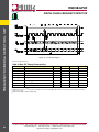
Figure 34. Lock Detect Window - Fractional Mode with Offset
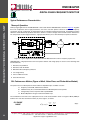
Lock Detect with Phase Measurement
Lock Detect with Phase Measurement is based on phase error measurement at the PFD output. The phase error
measurement is done in terms of the reference period at the PFD input. The period of the reference is first measured
with a delay line and this count is available in read-only register Reg 10h. The phase error at the output of the PFD
is then measured with the same delay line and this count is available in the read-only register Reg 11h. When the
PLL is not locked, the measured phase error count will vary every time the Reg 11h is read and will become a stable
value once PLL is locked. The phase error count will then be proportional to the static phase error at the PFD output.
For example, assuming that PLL is locked, if the reference duration count is 150 in Reg 10h and Reg 11h reads 35
then the approximate static phase error at the PFD output is 20*(35/150) = 4.7 ns assuming a 20 ns reference period
or Fpfd of 50 MHz. Reg 06h [13:0] defines the low and high thresholds for current phase error count. Reg 06h[23:14]
defines the number of reference cycles that the phase error has to be within the thresholds before the lock is declared.
For example, if the low threshold is set to Reg 06h [6:0] = 20d and high threshold is set to Reg 06h [13:7] = 50d and
the LD OK Count is set to Reg 06h[23:14] = 512d, then the phase error count has to be between 20 and 50 for 512
consecutive reference cycles before that lock is declared. The thresholds make it easier to define lock condition in
case of fractional operation where the static phase error is expected to be larger due to charge pump offset currents.
Chip Address Pins
HMC984LP4E has three programmable chip address bits, which enable the HMC984LP4E to be used in an SPI bus
configuration. Two LSB chip address bits are internal and bond wire programmable at the time of packaging. The MSB
bit is available externally as pin CHIP3. The chip address pins are read at power-up and every time the chip is reset.
By default, all CHIP3 is internally pulled to DVDD thus there is no need to connect the pin to DVDD if the address bit
is to be set as logic high. To assign a 0 to address bit, pin should be connected to ground. The internal CHIP1 and
CHIP2 bits are internally tied to ground.
FREQUENCY DIVIDERS & DETECTORS - SMT
DIGITAL PHASE-FREQUeNCY DETECTOR
The chip address for the companion chip HMC983LP5E is stored in Reg 09h[2:0] of HMC984LP4E. In cases when an
SPI command is common to both devices, it is not necessary to send separate commands to each part. Both parts
are always listening to the SPI bus and when a common command is issued, they will take the command and update
the corresponding registers. Writing its own chip address to the companion chip address register Reg 09h[2:0] will
disable this feature.
For price, delivery and to place orders: Hittite Microwave Corporation, 2 Elizabeth Drive, Chelmsford, MA 01824
978-250-3343 tel • 978-250-3373 fax • Order On-line at www.hittite.com
Application Support: [email protected]
6 - 25