1
HMC984LP4E
v02.0112
FREQUENCY DIVIDERS & DETECTORS - SMT
DIGITAL PHASE-FREQUeNCY DETECTOR
28
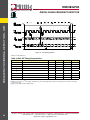
Figure 35. SPI Timing Diagram
DVDD = 5 V ±10%, GND = 0 V
Table 4. Main SPI Timing Characteristics
Parameter
Conditions
t1
SDI to SCK Setup Time
t2
t3
Min
Typ
Max
Units
8
nsec
SDI to SCK Hold Time
8
nsec
SCK High Duration [1]
10
nsec
t4
SCK Low Duration
10
nsec
t5
SEN Low Duration
20
nsec
t6
SEN High Duration
20
nsec
t7
SCK to SEN [2]
8
nsec
t8
SCK to SDO out
[3]
8
nsec
[1] The SPI is relatively insensitive to the duty cycle of SCK.
[2] SEN must rise after the 32nd falling edge of SCK but before the next rising SCK edge. If SCK is shared amongst several devices this timing
must be respected.
[3] Typical load to SDO is 10 pF, maximum 20 pF
For price, delivery and to place orders: Hittite Microwave Corporation, 2 Elizabeth Drive, Chelmsford, MA 01824
978-250-3343 tel • 978-250-3373 fax • Order On-line at www.hittite.com
Application Support: [email protected]