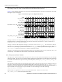
1
MIPS64 5K™ Processor Core Family Integrator’s Guide Document Number: MD00106 Revision 02.01 June 28, 2001 MIPS Technologies, Inc. 1225 Charleston Road Mountain View, CA 94043-1353 Copyright © 1999-2001 MIPS Technologies, Inc. All rights reserved. Unpublished rights reserved under the Copyright Laws of the United States of America. This document contains information that is proprietary to MIPS Technologies, Inc. (“MIPS Technologies”). Any copying, modifyingor use of this information (in whole or in part) which is not expressly permitted in writing by MIPS Technologies or a contractually-authorized third party is strictly prohibited. At a minimum, this information is protected under unfair competition laws and the expression of the information contained herein is protected under federal copyright laws. Violations thereof may result in criminal penalties and fines. MIPS Technologies or any contractually-authorized third party reserves the right to change the information contained in this document to improve function, design or otherwise. MIPS Technologies does not assume any liability arising out of the application or use of this information. Any license under patent rights or any other intellectual property rights owned by MIPS Technologies or third parties shall be conveyed by MIPS Technologies or any contractually-authorized third party in a separate license agreement between the parties. The information contained in this document constitutes one or more of the following: commercial computer software, commercial computer software documentation or other commercial items. If the user of this information, or any related documentation of any kind, including related technical data or manuals, is an agency, department, or other entity of the United States government (“Government”), the use, duplication, reproduction, release, modification, disclosure, or transfer of this information, or any related documentation of any kind, is restricted in accordance with Federal Acquisition Regulation 12.212 for civilian agencies and Defense Federal Acquisition Regulation Supplement 227.7202 for military agencies. The use of this information by the Government is further restricted in accordance with the terms of the license agreement(s) and/or applicable contract terms and conditions covering this information from MIPS Technologies or any contractually-authorized third party. MIPS, R3000, R4000, R5000, R8000 and R10000 are among the registered trademarks of MIPS Technologies, Inc., and R4300, R20K, MIPS16, MIPS32, MIPS64, MIPS-3D, MIPS I, MIPS II, MIPS III, MIPS IV, MIPS V, MDMX, SmartMIPS, 4K, 4Kc, 4Km, 4Kp, 5K, 5Kc, 20K, 20Kc, EC, MGB, SOC-it, SEAD, YAMON, ATLAS, JALGO, CoreLV and MIPS-based are among the trademarks of MIPS Technologies, Inc. All other trademarks referred to herein are the property of their respective owners. MIPS64 5K™ Processor Core Family Integrator’s Guide, Revision 02.01 Table of Contents Chapter 1 Introduction ..........................................................................................................................................................1 Chapter 2 EC Interface ..........................................................................................................................................................3 2.1 Introduction .............................................................................................................................................................3 2.1.1 Features .........................................................................................................................................................3 2.1.2 Basic Operation .............................................................................................................................................4 2.2 EC Interface Signal Descriptions ............................................................................................................................5 2.3 Interface Transactions .............................................................................................................................................7 2.3.1 Single Read Transactions ..............................................................................................................................8 2.3.2 Single Write Transactions ...........................................................................................................................10 2.3.3 Back-to-back Read Transactions ................................................................................................................13 2.3.4 Back-to-back Write Transactions ...............................................................................................................14 2.3.5 Read Transaction Followed by a Write Transaction ...................................................................................15 2.3.6 Write Transaction Followed by a Read Transaction ...................................................................................17 2.3.7 Burst Transactions ......................................................................................................................................18 2.4 External Write Buffers ..........................................................................................................................................22 2.5 Endianess ..............................................................................................................................................................23 2.6 Lower Address Bits ...............................................................................................................................................24 Chapter 3 System Interface .................................................................................................................................................27 3.1 Introduction ...........................................................................................................................................................27 3.2 System Interface Signal Descriptions ...................................................................................................................27 Chapter 4 Coprocessor Interface .........................................................................................................................................31 4.1 Introduction ...........................................................................................................................................................31 4.2 Coprocessor Instructions .......................................................................................................................................31 4.3 Coprocessor Interface Signal Descriptions ...........................................................................................................33 4.4 Coprocessor Attachment to the 5K Family ...........................................................................................................41 4.4.1 5Kc Coprocessor Attachment .....................................................................................................................42 4.4.2 5Kf Coprocessor Attachment ......................................................................................................................42 4.4.3 COP2 Data Transfer Width .........................................................................................................................42 4.4.4 Out-of-Order Data Transfers .......................................................................................................................42 4.4.5 Limited Dual Issue ......................................................................................................................................43 4.5 Interface Protocols ................................................................................................................................................43 4.5.1 Instruction Dispatch ....................................................................................................................................47 4.5.2 To Coprocessor Data Transfer ....................................................................................................................48 4.5.3 From Coprocessor Data Transfer ................................................................................................................49 4.5.4 Condition Code Checking ...........................................................................................................................50 4.5.5 GPR Data ....................................................................................................................................................50 4.5.6 Coprocessor Exceptions ..............................................................................................................................51 4.5.7 Instruction Nullification ..............................................................................................................................51 4.5.8 Instruction Killing .......................................................................................................................................52 4.5.9 Hardware Present Signaling ........................................................................................................................52 4.5.10 Coprocessor Idle .......................................................................................................................................53 4.5.11 Reset ..........................................................................................................................................................53 Chapter 5 EJTAG Interface .................................................................................................................................................55 5.1 Introduction ...........................................................................................................................................................55 5.2 EJTAG Interface Signal Descriptions ...................................................................................................................55 5.3 Test Access Port Interface Descriptions ...............................................................................................................58 5.3.1 TAP Reset ...................................................................................................................................................59 5.3.2 TAP Controller ............................................................................................................................................59 MIPS64 5K™ Processor Core Family Integrator’s Guide, Revision 02.01 iii 5.3.3 TAP Operation Example .............................................................................................................................61 5.4 Reset from Probe ...................................................................................................................................................62 Chapter 6 Production Test Interface ....................................................................................................................................63 6.1 Introduction ...........................................................................................................................................................63 6.2 Production Test Interface Signal Descriptions ......................................................................................................63 6.3 Internal Scan Interface ..........................................................................................................................................64 6.4 User-Implemented RAM BIST Interface ..............................................................................................................64 6.5 Integrated Memory BIST for Cache RAMs Interface ...........................................................................................65 Chapter 7 Clocking, Reset, and Power ................................................................................................................................67 7.1 Introduction ...........................................................................................................................................................67 7.2 Clocking ................................................................................................................................................................67 7.2.1 SI_ClkIn Clock ...........................................................................................................................................67 7.2.2 EJ_TCK Clock ............................................................................................................................................68 7.2.3 Handling Clock Insertion Delay .................................................................................................................68 7.3 Core Reset and NMI .............................................................................................................................................68 7.3.1 SI_ColdReset ..............................................................................................................................................69 7.3.2 SI_Reset ......................................................................................................................................................69 7.3.3 SI_NMI .......................................................................................................................................................69 7.4 Power Management ...............................................................................................................................................69 7.4.1 Reducing SI_ClkIn Frequency ....................................................................................................................69 7.4.2 Software-Induced Sleep Mode ....................................................................................................................70 Chapter 8 Simulation Models ..............................................................................................................................................71 8.1 Installing the VMC Model ....................................................................................................................................71 8.2 Verifying the VMC Installation ............................................................................................................................72 8.3 SWIFT Template Generation ................................................................................................................................72 8.4 Back-annotating with SDF Timing .......................................................................................................................73 8.5 Register Windows .................................................................................................................................................73 8.6 VMC Simulation Configuration ............................................................................................................................73 8.7 Multiple VMC Instances .......................................................................................................................................75 8.8 Assertion Checks ...................................................................................................................................................75 Appendix A Revision History .............................................................................................................................................77 iv MIPS64 5K™ Processor Core Family Integrator’s Guide, Revision 02.01 List of Figures Figure 2-1: Fastest Single Read Transaction Timing ...........................................................................................................9 Figure 2-2: Single Read Transaction Timing (3 Data Wait States)....................................................................................10 Figure 2-3: Fastest Single Write Transaction Timing ........................................................................................................11 Figure 2-4: Single Write Transaction Timing (1 Address Wait State and 4 Data Wait States) .........................................12 Figure 2-5: Back-to-back Read Transaction Timing..........................................................................................................13 Figure 2-6: Back-to-back Write Transaction Timing .........................................................................................................14 Figure 2-7: Read Transaction Followed by a Write Transaction .......................................................................................15 Figure 2-8: Read Transaction Followed by a Write Transaction with Reordering ............................................................16 Figure 2-9: Write Transaction Followed by a Read Transaction .......................................................................................17 Figure 2-10: Write Transaction Followed by a Read Transaction with Reordering ..........................................................18 Figure 2-11: Burst Read Transaction Timing.....................................................................................................................20 Figure 2-12: Burst Write Transaction Timing....................................................................................................................22 Figure 2-13: Example of Generating Low Address Bits ....................................................................................................25 Figure 4-1: Block Diagram of Coprocessor Interface ........................................................................................................41 Figure 4-2: General Transfer Example...............................................................................................................................45 Figure 4-3: Arithmetic Coprocessor Dispatch Waveform..................................................................................................48 Figure 4-4: To Coprocessor Data Transfer Waveform.......................................................................................................49 Figure 4-5: From Coprocessor Data Transfer Waveform ..................................................................................................50 Figure 5-1: Test Access Port (TAP) Overview ..................................................................................................................58 Figure 5-2: TAP Controller State Diagram ........................................................................................................................59 Figure 5-3: EJ_TDI to EJ_TDO Path when in Shift-IR State ............................................................................................60 Figure 5-4: EJ_TDI to EJ_TDO Path for Selected Data Register(s) when in Shift-DR State ...........................................61 Figure 5-5: EJ_TDI to EJ_TDO Path when in Shift-DR State and ALL Instruction is Selected.......................................61 Figure 5-6: TAP Operation Example .................................................................................................................................61 Figure 6-1: Protocol for Use of Integrated Memory BIST for Cache RAMs ....................................................................65 MIPS64 5K™ Processor Core Family Integrator’s Guide, Revision 02.01 v vi MIPS64 5K™ Processor Core Family Integrator’s Guide, Revision 02.01 List of Tables Table 2-1: Signal Direction Key...........................................................................................................................................5 Table 2-2: EC Interface Signals ...........................................................................................................................................5 Table 2-3: Burst Order for Sequential Ordering (4 Beat Bursts) .......................................................................................20 Table 2-4: Burst Order for Sub-block Ordering (4 Beat Bursts)........................................................................................21 Table 2-5: Endian Examples ..............................................................................................................................................23 Table 3-1: Signal Direction Key.........................................................................................................................................27 Table 3-2: System Interface Signal Descriptions ...............................................................................................................28 Table 4-1: Signal Direction Key.........................................................................................................................................34 Table 4-2: Signal Coprocessor Category............................................................................................................................34 Table 4-3: Combined Issue Group 0 Signals - Used for both COP1 and COP2 ................................................................34 Table 4-4: Combined Issue Group 0 Signals - Used only for COP1..................................................................................37 Table 4-5: Combined Issue Group 0 Signals - Used only for COP2..................................................................................38 Table 4-6: Arithmetic Issue Group 1 Signals - Used for both COP1 and COP2 ...............................................................39 Table 4-7: Arithmetic Issue Group 1 Signals - Used only for COP1 .................................................................................40 Table 4-8: Arithmetic Issue Group 1 Signals - Used only for COP2 .................................................................................41 Table 4-9: Transfers Required for Each Dispatch ..............................................................................................................44 Table 4-10: Allowable Interface Latencies from a Coprocessor to the 5K Core ...............................................................46 Table 4-11: Interface Latencies From the 5K Core to a Coprocessor ................................................................................46 Table 5-1: Signal Direction Key.........................................................................................................................................56 Table 5-2: System Interface Signal Descriptions ...............................................................................................................56 Table 6-1: Signal Direction Key.........................................................................................................................................63 Table 6-2: Production Test Interface Signal Descriptions .................................................................................................64 Table 8-1: VMC Configuration Options ............................................................................................................................73 MIPS64 5K™ Processor Core Family Integrator’s Guide, Revision 02.01 vii viii MIPS64 5K™ Processor Core Family Integrator’s Guide, Revision 02.01 Chapter 1 Introduction The MIPS64 5K Processor Core Family Integrator’s Guide is targeted for the ASIC designer who is integrating a version of the MIPS64 5K processor core into his/her system ASIC. This document is applicable to both those integrators who are using a hard core and those who are integrating a soft core. The following chapters describe the interface to the 5K core, including descriptions of the pins of the core as well as a description of the protocols used: • Chapter 2 describes the external system bus, EC™ interface, of the core. • Chapter 3 describes the general system control signals used by the core. • Chapter 4 describes the COP interface used by the core for attaching tightly coupled coprocessor units. • Chapter 5 describes the EJTAG interface used by the core, including the EJTAG TAP interface and controller. • Chapter 6 describes the internal scan and memory test interface used by the core for production test. • Chapter 7 describes how to properly clock and reset the core. Reset and power management is also covered in this chapter. MIPS64 5K™ Processor Core Family Integrator’s Guide, Revision 02.01 1 Chapter 1 Introduction 2 MIPS64 5K™ Processor Core Family Integrator’s Guide, Revision 02.01 Chapter 2 EC Interface This chapter describes the 5K EC interface, which allows the 5K core access to instruction and data memory as well as I/O devices. It contains the following sections: • Section 2.1, "Introduction" • Section 2.2, "EC Interface Signal Descriptions" • Section 2.3, "Interface Transactions" • Section 2.4, "External Write Buffers" • Section 2.5, "Endianess" • Section 2.6, "Lower Address Bits" 2.1 Introduction The EC interface is implemented in the 5K core as follows: • Data buses are 64 bits wide • Address lines EB_A[35:3] are used • The maximum number of outstanding transactions is 16 (8 reads and 8 writes). Also note the following 5K-specific feature: on a WAIT instruction, the 5K core waits until the internal write buffer is empty before entering low-power mode. 2.1.1 Features The 64-bit implementation of the EC interface has the following features: • 64-bit data buses • 36-bit addressing • Separate read and write data buses • All signals are unidirectional—no bidirectional or 3-state buses • Fully registered, synchronous interface to the 5K core • Separate read and write bus error indications • Separate address and data phases allow pipelining on the interface • No limit on the number of outstanding transactions • Number of outstanding transactions can be limited by the external logic • Support for variable burst length • Sequential or sub-block ordering burst address sequences • Indication of first and last address phase of a burst • Request for emptying external write buffers and indication of external write buffers being empty MIPS64 5K™ Processor Core Family Integrator’s Guide, Revision 02.01 3 Chapter 2 EC Interface • Byte enable indication • Indication of instruction read (fetch) • Address and data phases can complete the same cycle they are initiated (zero wait states) • No limit on the number of wait states in address and data phases • Independent read and write data phases. A read transaction can overtake a write transaction and vice versa. • Only one 5K core and one external logic 2.1.2 Basic Operation All inputs to the 5K core are sampled at the rising edge of the SI_ClkIn signal. Further the outputs from the 5K core change with respect to a rising edge of the SI_ClkIn signal. The EC interface does not include a signal to indicate reset. Therefore to reset the EC interface, reset the 5K core and the external logic simultaneously. Whenever the EC interface is reset, all transactions are aborted and the bus returns to the idle state. EB_ARdy, EB_AValid, EB_WDRdy, EB_RdVal, EB_Burst, EB_BFirst, EB_BLast, EB_RBErr, and EB_WBErr must be driven inactive during reset. Each transaction on the EC interface has an address phase and a data phase, which can have a number of wait states. A wait state in the address phase is named an address wait state and is defined as a clock cycle where EB_AValid is asserted and EB_ARdy was sampled deasserted in the beginning of the cycle. An address phase begins in the clock cycle where the 5K core asserts EB_AValid. An address phase ends on the positive clock edge following an asserted sample of EB_ARdy. For maximum speed (no address wait states), EB_ARdy has to be sampled asserted on the positive clock edge preceding the beginning of the address phase. During an address phase, all signals driven by the 5K core are unchanged and stable (except from the write data bus, EB_WData). Due to the separate read and write data buses, two types of data phases exist: the read data phase and the write data phase. A wait state in a data phase is named a data wait state. It is defined as a clock cycle where the corresponding address phase has been started (and possibly ended) and: • For a write data phase, EB_WDRdy is sampled deasserted at the beginning of the cycle • For a read data phase, EB_RdVal is sampled deasserted at the end of the cycle A read data phase begins in the clock cycle where the 5K core starts the corresponding read address phase. However, if there are outstanding read data phases when the read address phase begins, the corresponding read data phase does not start until all of the preceding read data phases have ended. The read data phase ends at the positive clock edge where EB_RdVal is sampled asserted. It can not end earlier than when the corresponding address phase ends. A write data phase begins in the clock cycle where the 5K core starts the corresponding write address phase. However, if there are outstanding write data phases when the write address phase begins, the corresponding write data phase does not start until all of the preceding write data phases have ended. The write data phase ends at the positive clock edge following the positive clock edge where EB_WDRdy is sampled asserted. For maximum speed (no data wait states), EB_WDRdy must be asserted on the positive clock edge preceding the beginning of the corresponding address phase. It cannot end earlier than the corresponding address phase ends. From these definitions, for a given transaction the number of data wait states must be greater than or equal to the number of address wait states. 4 MIPS64 5K™ Processor Core Family Integrator’s Guide, Revision 02.01 2.2 EC Interface Signal Descriptions 2.2 EC Interface Signal Descriptions This section describes the signals of the 5K processor core’s EC Interface. Table 2-1 provides the pin direction key for the signal descriptions. Note that all outputs are driven directly from flops and all inputs are input directly to flops. A clock cycle begins on a rising edge and ends just before the next rising edge. Table 2-1 Signal Direction Key Dir Description I Input to the 5K core. Unless otherwise noted, input signals are sampled on the rising edge of the appropriate CLK signal. O Output from the 5K core. Unless otherwise noted, output signals are driven on the rising edge of the appropriate CLK signal. SI Static input to the 5K core. These signals are normally tied to either power or ground and should not change state while SI_Reset is deasserted. The signals are described in Table 2-2. Note that the signals are listed alphabetically. Table 2-2 EC Interface Signals Signal Name Dir Description EB_A[35:3] O Address bus. Only valid when EB_AValid is asserted. EB_ARdy I Assertion of this signal indicates whether the external logic is ready for a new address. The 5K core does not complete the address phase until the clock cycle after EB_ARdy is sampled asserted. EB_AValid O Assertion of this signal indicates that the values on the address bus and access type lines are valid (signifying an address phase is ongoing). EB_AValid is always valid and cannot be deasserted between address phases within a burst. MIPS64 5K™ Processor Core Family Integrator’s Guide, Revision 02.01 5 Chapter 2 EC Interface Table 2-2 EC Interface Signals (Continued) Signal Name Dir Description Indicates which bytes of the EB_RData or EB_WData buses are involved in the data phase corresponding to the current address phase. If an EB_BE signal is asserted, the associated byte is being read or written. EB_BE lines are only valid while EB_AValid is asserted. During bursts all lines must be asserted. The table below lists the values that EB_BE can take. Byte enables supported EB_BE[7:0] O 00000001 00000010 00000100 00001000 00010000 00100000 01000000 10000000 11000000 00110000 00001100 00000011 11100000 01110000 00001110 00000111 11110000 00001111 11111000 00011111 11111100 00111111 11111110 01111111 11111111 EB_BE Signal Read Data Bits Sampled Write Data Bits Driven Valid EB_BE[0] EB_RData[7:0] EB_WData[7:0] EB_BE[1] EB_RData[15:8] EB_WData[15:8] EB_BE[2] EB_RData[23:16] EB_WData[23:16] EB_BE[3] EB_RData[31:24] EB_WData[31:24] EB_BE[4] EB_RData[39:32] EB_WData[39:32] EB_BE[5] EB_RData[47:40] EB_WData[47:40] EB_BE[6] EB_RData[55:48] EB_WData[55:48] EB_BE[7] EB_RData[63:56] EB_WData[63:56] EB_BFirst O Assertion of this signal indicates the address phase is the first address phase of a burst. EB_BFirst is always valid. EB_BLast O Assertion of this signal indicates the address phase is the last address phase of a burst. Note that the time for assertion of EB_BLast is determined by use of EB_Burst, EB_BFirst, and EB_BLen. EB_BLast is always valid. EB_BLen[1:0] indicate the length (number of address/data phases) of the burst. This signal is an implementation-specific static output. EB_BLen[1:0] Burst Length 0 reserved 1 4 2 reserved 3 reserved EB_Burst O Assertion of this signal indicates that the current address phase is for a cache fill or a write burst. EB_Burst is always valid. EB_BusClkActive I Must be driven HIGH I Indicates that all external write buffers are empty. The external write buffers must deassert EB_EWBE in the cycle following the assertion of the corresponding EB_WDRdy and keep EB_EWBE deasserted until the external write buffers are empty. See Section 2.4, "External Write Buffers" on page 22 for more details. EB_EWBE 6 O EB_BLength[1:0] MIPS64 5K™ Processor Core Family Integrator’s Guide, Revision 02.01 2.3 Interface Transactions Table 2-2 EC Interface Signals (Continued) Signal Name Dir Description EB_Instr O Assertion of this signal indicates that the address is for an instruction fetch as opposed to a data read. EB_Instr is only valid when EB_AValid is asserted. EB_RBErr I Bus error indicator for read transactions. EB_RBErr is always valid. Only assert it in the same cycle that the corresponding EB_RdVal is asserted. EB_RData[63:0] I Read data bus. Valid at the end of a read data phase (on the rising clock edge where EB_RdVal is sampled asserted). EB_RdVal I Assertion of this signal indicates that the external logic is driving read data on EB_RData (it ends a read data phase). EB_RdVal must always be valid. EB_RdVal must never be asserted until after the corresponding EB_ARdy is sampled asserted. EB_SBlock SI When this signal is asserted, sub-block ordering is used for addressing bursts. When this signal is deasserted, sequential addressing is used. See Section 2.3.7, "Burst Transactions" on page 18 for details. EB_WBErr I Bus error indicator for write transactions. EB_WBErr is always valid. Only assert it in the cycle following an asserted sample of the corresponding EB_WDRdy. EB_WData[63:0] O Write data bus. Kept unchanged and stable during a write data phase until the write data phase ends (the positive clock edge following an asserted sample of EB_WDRdy). EB_WDRdy I Assertion of this signal indicates that the external logic is ready to process a write; it ends a write data phase and the EB_WData can change after the positive clock edge that follows the positive clock edge where EB_WDRdy is sampled asserted. EB_WDRdy is not sampled until the rising edge where the corresponding EB_ARdy is sampled asserted. EB_Write O Assertion of this signal indicates that the address phase is for a write. Deassertion of this signal indicates that the address phase is for a read. This signal is only valid when EB_AValid is asserted. O Assertion of this signal indicates that the 5K core is waiting for external write buffers to empty. EB_WWBE can be asserted when EB_EWBE is asserted, but if EB_EWBE is deasserted and EB_WWBE is asserted, EB_EWBE must be asserted eventually. See Section 2.4, "External Write Buffers" on page 22 for more details. EB_WWBE 2.3 Interface Transactions The 5K core implements a unidirectional data-bus mode that uses separate busses for each direction. EB_RData[63:0] is used for read operations, and EB_WData[63:0] is used for write operations. The address phase of a bus transaction (all signals except the data transfer and bus error indication) is separated from the data phase (data transfer and bus error indication), that is, the address phase of a transaction can complete before the corresponding data phase begins. The bus transactions listed below are described in the following subsections: • Fastest read • Single read with wait states • Fastest write • Single write with wait states • Back-to-back read • Back-to-back write MIPS64 5K™ Processor Core Family Integrator’s Guide, Revision 02.01 7 Chapter 2 EC Interface • Read followed by write • Read followed by write with reordering • Write followed by read • Write followed by read with reordering • Burst read • Burst write The 5K core supports the following outstanding bus transactions (adding up to a maximum of 16 outstanding transactions): • 1 burst data read (4 reads) or a single data read • 1 burst instruction read (4 reads) or a single instruction read • 1 eviction of a dirty line (4 writes) • 1 accelerated write burst (4 writes) or 4 single writes 2.3.1 Single Read Transactions Figure 2-1 shows the basic timing relationships between signals during a simple (fastest) read transaction. When the 5K core is ready to begin a bus transaction (cycle 3), the address is driven on EB_A, the associated control information is driven on EB_Instr, EB_Burst, EB_BFirst, EB_BLast, EB_BLen, EB_Write, and EB_BE, and EB_AValid is asserted. On the same rising clock edge that these signals are driven out (end of cycle 2), the EB_ARdy signal state is sampled. If EB_ARdy is sampled deasserted, the 5K core maintains the transaction values on the previously mentioned signals. The 5K core continues driving valid and stable values on these interface signals until the rising clock edge following the one that the EB_ARdy signal is sampled asserted. Starting in the same cycle as the read transaction is initiated, the 5K core samples EB_RdVal, EB_RData, and EB_RBErr. These signals are sampled on each rising clock edge until the EB_RdVal signal is sampled asserted. The data values sampled with this asserted EB_RdVal are considered valid. However, if EB_RBErr was sampled asserted in same cycle, the transaction is considered failed. Note that the data phase cannot end earlier than the corresponding address phase. EB_ARdy must be sampled asserted at least one clock cycle before the corresponding EB_RdVal is sampled asserted. 8 MIPS64 5K™ Processor Core Family Integrator’s Guide, Revision 02.01 2.3 Interface Transactions Cycle # 1 2 3 4 5 6 7 8 9 10 SI_ClkIn EB_ARdy EB_A A1 EB_AValid EB_Instr Valid EB_Write EB_BE BE1 EB_Burst EB_BFirst EB_BLast EB_BLen EB_RData Valid RD1 EB_RBErr EB_RDVal EB_WData EB_WBErr EB_WDRdy Figure 2-1 Fastest Single Read Transaction Timing MIPS64 5K™ Processor Core Family Integrator’s Guide, Revision 02.01 9 Chapter 2 EC Interface Figure 2-2 shows an example of a read transaction with three wait states in the data phase (indicated by the deassertion of EB_RdVal for three clock cycles). EB_RdVal is sampled deasserted on the rising edges at the beginning of cycles 4, 5, and 6 and then is asserted on cycle 7. Cycle # 1 2 3 4 5 6 7 8 9 10 SI_ClkIn EB_ARdy EB_A A1 EB_AValid EB_Instr Valid EB_Write EB_BE BE1 EB_Burst EB_BFirst EB_BLast EB_BLen Valid EB_RData RD1 EB_RBErr EB_RDVal EB_WData EB_WBErr EB_WDRdy Figure 2-2 Single Read Transaction Timing (3 Data Wait States) 2.3.2 Single Write Transactions Figure 2-3 shows a zero wait state (fastest) write transaction. Like the read transaction when a write request is issued (cycle 3), the address and control information for the transaction are driven on EB_A, EB_Instr, EB_Burst, EB_BFirst, EB_BLast, EB_BLen, EB_Write, and EB_BE. These signals remain unchanged until the rising clock edge after the EB_ARdy signal is sampled asserted. The write data is driven on the write data bus, EB_WData, in same cycle as the address is driven on EB_A. The write data is held on the bus until the rising clock edge after EB_WDRdy is sampled asserted. 10 MIPS64 5K™ Processor Core Family Integrator’s Guide, Revision 02.01 2.3 Interface Transactions EB_WBErr is sampled on the first rising clock edge after the rising clock edge that EB_WDRdy is sampled asserted. If EB_WBErr is asserted at this time, the bus transaction is considered failed. Note that the data phase cannot end earlier than the corresponding address phase. EB_WDRdy must be sampled asserted on the same clock edge or later than the clock edge where the corresponding EB_ARdy is sampled asserted. Cycle # 1 2 3 4 5 6 7 8 9 10 SI_ClkIn EB_ARdy EB_A A1 EB_AValid EB_Instr Valid EB_Write EB_BE BE1 EB_Burst EB_BFirst EB_BLast EB_BLen Valid EB_RData EB_RBErr EB_RDVal EB_WData WD1 EB_WBErr EB_WDRdy Figure 2-3 Fastest Single Write Transaction Timing MIPS64 5K™ Processor Core Family Integrator’s Guide, Revision 02.01 11 Chapter 2 EC Interface Figure 2-4 shows an example of a write transaction with four data wait states, indicated by the deassertion of the EB_WDRdy signal. EB_WDRdy is deasserted for four clock cycles, and then asserted. Note that the address phase is prolonged by one clock cycle because EB_ARdy is deasserted for one clock cycle (sampled deasserted at the end of cycle 2). Cycle # 1 2 3 4 5 6 7 8 9 10 SI_ClkIn EB_ARdy EB_A A1 EB_AValid EB_Instr Valid EB_Write EB_BE BE1 EB_Burst EB_BFirst EB_BLast EB_BLen Valid EB_RData EB_RBErr EB_RDVal EB_WData WD1 EB_WBErr EB_WDRdy Figure 2-4 Single Write Transaction Timing (1 Address Wait State and 4 Data Wait States) 12 MIPS64 5K™ Processor Core Family Integrator’s Guide, Revision 02.01 2.3 Interface Transactions 2.3.3 Back-to-back Read Transactions Figure 2-5 shows an example of two consecutive read transactions, which shows the ability to pipeline read addresses independent of data wait states. Through manipulation of the EB_ARdy signal, the external logic can limit the depth of the address pipelining. Cycle # 1 2 3 4 5 6 7 8 9 10 SI_ClkIn EB_ARdy EB_A A1 A2 Valid Valid BE1 BE2 Valid Valid EB_AValid EB_Instr EB_Write EB_BE EB_Burst EB_BFirst EB_BLast EB_BLen EB_RData RD1 RD2 EB_RBErr EB_RDVal EB_WData EB_WBErr EB_WDRdy Figure 2-5 Back-to-back Read Transaction Timing MIPS64 5K™ Processor Core Family Integrator’s Guide, Revision 02.01 13 Chapter 2 EC Interface 2.3.4 Back-to-back Write Transactions Figure 2-6 shows an example of two consecutive write transactions. Similar to the read transactions, pipelining of write addresses can occur regardless of data wait states. Cycle # 1 2 3 4 5 6 7 8 9 10 SI_ClkIn EB_ARdy EB_A A1 A2 Valid Valid BE1 BE2 Valid Valid EB_AValid EB_Instr EB_Write EB_BE EB_Burst EB_BFirst EB_BLast EB_BLen EB_RData EB_RBErr EB_RDVal EB_WData WD1 WD2 EB_WBErr EB_WDRdy Figure 2-6 Back-to-back Write Transaction Timing 14 MIPS64 5K™ Processor Core Family Integrator’s Guide, Revision 02.01 2.3 Interface Transactions 2.3.5 Read Transaction Followed by a Write Transaction Figure 2-7 shows the relationship between a read transaction and a subsequent write transaction. A write transaction following a read transaction behaves as described for the single write transaction. Completion of these transactions out of order is allowed. Cycle # 1 2 3 4 A1 A2 Valid Valid BE1 BE2 Valid Valid 5 6 7 8 9 10 SI_ClkIn EB_ARdy EB_A EB_AValid EB_Instr EB_Write EB_BE EB_Burst EB_BFirst EB_BLast EB_BLen EB_RData RD1 EB_RBErr EB_RDVal EB_WData WD2 EB_WBErr EB_WDRdy Figure 2-7 Read Transaction Followed by a Write Transaction MIPS64 5K™ Processor Core Family Integrator’s Guide, Revision 02.01 15 Chapter 2 EC Interface Figure 2-8 shows an example of a read transaction followed by a write transaction where the write transaction is completed prior to the read transaction (out of order). Cycle # 1 2 3 4 A1 A2 Valid Valid BE1 BE2 Valid Valid 5 6 7 8 9 10 SI_ClkIn EB_ARdy EB_A EB_AValid EB_Instr EB_Write EB_BE EB_Burst EB_BFirst EB_BLast EB_BLen EB_RData RD1 EB_RBErr EB_RDVal EB_WData WD2 EB_WBErr EB_WDRdy Figure 2-8 Read Transaction Followed by a Write Transaction with Reordering 16 MIPS64 5K™ Processor Core Family Integrator’s Guide, Revision 02.01 2.3 Interface Transactions 2.3.6 Write Transaction Followed by a Read Transaction Figure 2-9 shows an example of a write transaction followed by a read. As in the case of a write following a read, a read transaction following a write transaction is not affected by the behavior of the write transaction. Completion of these transactions out of order is allowed. Cycle # 1 2 3 4 5 A1 A2 Valid Valid BE1 BE2 Valid Valid 6 7 8 9 10 SI_ClkIn EB_ARdy EB_A EB_AValid EB_Instr EB_Write EB_BE EB_Burst EB_BFirst EB_BLast EB_BLen EB_RData RD2 EB_RBErr EB_RDVal EB_WData WD1 EB_WBErr EB_WDRdy Figure 2-9 Write Transaction Followed by a Read Transaction MIPS64 5K™ Processor Core Family Integrator’s Guide, Revision 02.01 17 Chapter 2 EC Interface Figure 2-10 shows an example of a write transaction followed by a read transaction where the read transaction is completed prior to the write transaction (out of order). Cycle # 1 2 3 4 5 A1 A2 Valid Valid BE1 BE2 Valid Valid 6 7 8 9 10 SI_ClkIn EB_ARdy EB_A EB_AValid EB_Instr EB_Write EB_BE EB_Burst EB_BFirst EB_BLast EB_BLen EB_RData RD2 EB_RBErr EB_RDVal EB_WData WD1 EB_WBErr EB_WDRdy Figure 2-10 Write Transaction Followed by a Read Transaction with Reordering 2.3.7 Burst Transactions A burst transaction initiates the transfer of multiple related transfers. Read bursts are used to read data to be placed in the instruction or data cache. Write bursts are used to empty the contents of the write buffers. Note that initiated bursts are always completed. The burst transaction cannot be aborted before reaching the burst beat count (indicated by EB_BLen) except in the case where the EC interface is reset. EB_Burst is asserted during the entire burst address sequence. EB_BFirst is driven asserted during the first address phase of the burst and is deasserted with each of the remaining address phases. EB_BLast is driven asserted during the last 18 MIPS64 5K™ Processor Core Family Integrator’s Guide, Revision 02.01 2.3 Interface Transactions address phase and is deasserted with all prior address phases. Apart from EB_Burst, EB_BFirst and EB_BLast behavior, and the deterministic address sequence, the multiple transfers of a burst transaction behave like that of back-to-back single transactions, which simplifies interfacing to systems that do not support burst transactions. Note that it is possible in the presence of data wait states, for all of the burst address phases to complete before the first data phase of the burst (or even of a preceding transaction) has completed. If this behavior is undesirable, EB_ARdy can be used to control the pace at which the addresses are transferred. Note that EB_AValid cannot be deasserted between address phases within a burst and that all bits in EB_BE must be asserted in all address phases within a burst. Figure 2-11 shows an example of a read burst transaction. EB_BLen indicates the length of the burst (see Section 2.2, "EC Interface Signal Descriptions" on page 5 for further information on EB_BLen). The data requested is always an aligned block according to the EB_BLen signal. The order of the words within the block varies depending on which word in the block is being requested and the value of EB_SBlock (see Table 2-3 and Table 2-4 for further information on the refill scheme). MIPS64 5K™ Processor Core Family Integrator’s Guide, Revision 02.01 19 Chapter 2 EC Interface Cycle # 1 2 3 4 5 6 7 A1 A2 A3 A4 Valid Valid Valid Valid 8 9 10 SI_ClkIn EB_ARdy EB_A EB_AValid EB_Instr EB_Write All asserted EB_BE EB_Burst EB_BFirst EB_BLast Valid EB_BLen EB_RData RD1 RD2 RD3 RD4 EB_RBErr EB_RDVal EB_WData EB_WBErr EB_WDRdy Figure 2-11 Burst Read Transaction Timing Table 2-3 and Table 2-4 show the possible sequences for the least significant address bits during a burst. Table 2-3 Burst Order for Sequential Ordering (4 Beat Bursts) Req DWord Address 20 (EB_A[4:3]) Sequence 0 0 1 2 3 1 1 2 3 0 2 2 3 0 1 3 3 0 1 2 MIPS64 5K™ Processor Core Family Integrator’s Guide, Revision 02.01 2.3 Interface Transactions Table 2-4 Burst Order for Sub-block Ordering (4 Beat Bursts) Req DWord Address (EB_A[4:3]) Sequence 0 0 1 2 3 1 1 0 3 2 2 2 3 0 1 3 3 2 1 0 MIPS64 5K™ Processor Core Family Integrator’s Guide, Revision 02.01 21 Chapter 2 EC Interface Figure 2-12 shows a burst write. Burst write transactions are used to empty write buffers. Write burst addresses always start at the lowest address of an address block according to the EB_BLen indication. Note that like single transactions, burst read and write transactions can complete out of order. Burst reads can overtake burst writes and vice versa. Cycle # 1 2 3 4 5 6 A1 A2 A3 A4 Valid Valid Valid Valid 7 8 9 10 SI_ClkIn EB_ARdy EB_A EB_AValid EB_Instr EB_Write All asserted EB_BE EB_Burst EB_BFirst EB_BLast Valid EB_BLen EB_RData EB_RBErr EB_RDVal EB_WData WD1 WD2 WD3 WD4 EB_WBErr EB_WDRdy Figure 2-12 Burst Write Transaction Timing 2.4 External Write Buffers Some systems might have external write buffers to increase bus efficiency and system performance. The 5K core has a two-signal interface that allows software to have some control over the external write buffers. The SYNC instruction is intended to form a barrier between load/store instructions before and after it in the instruction stream. Upon execution of a SYNC instruction, the 5K core completes all pending read requests and flush the internal write buffer. The 5K core 22 MIPS64 5K™ Processor Core Family Integrator’s Guide, Revision 02.01 2.5 Endianess also asserts EB_WWBE to signal to the system that it is Waiting for the Write Buffer Empty signal. The SYNC instruction does not complete until the EB_EWBE input is asserted. In most systems you can tie EB_EWBE high. Just using EB_WWBE does not ensure coherency. If a write is in the external write buffer, the core can generate a read request to the given address without asserting EB_WWBE (because the core has no knowledge of the external write buffers). Therefore, any write buffers in the system must maintain coherency with reads. The EB_WWBE/EB_EWBE interface can be used to make SYNCs “harder” by forcing the flush of the external write buffers in addition to flushing internal write buffers. This method is a system/software design issue—you need to decide what if anything you want the system to do when a SYNC instruction is executed. 2.5 Endianess To help understand the use of endianess, Table 2-5 shows some cases of how stores appear on the EC interface in little-endian and big-endian mode. Table 2-5 Endian Examples Internal Addr[2:0] Big-endian Little-endian EB_D[63:0] EB_BE [7:0] EB_D[63:0] EB_BE [7:0] lui t0, 0x0123 ori t0, t0, 0x4567 dsll t0, t0, 16 ori t0, t0, 0x89ab dsll t0, t0, 16 ori t0, t0, 0xcdef sb t0, 0x0(r0) 0 0xefXXXXXXXXXXXXXX 10000000 0xXXXXXXXXXXXXXXef 00000001 sb t0, 0x1(r0) 1 0xXXefXXXXXXXXXXXX 01000000 0xXXXXXXXXXXXXefXX 00000010 sb t0, 0x2(r0) 2 0xXXXXefXXXXXXXXXX 00100000 0xXXXXXXXXXXefXXXX 00000100 sb t0, 0x3(r0) 3 0xXXXXXXefXXXXXXXX 00010000 0xXXXXXXXXefXXXXXX 00001000 sb t0, 0x4(r0) 4 0xXXXXXXXXefXXXXXX 00001000 0xXXXXXXefXXXXXXXX 00010000 sb t0, 0x5(r0) 5 0xXXXXXXXXXXefXXXX 00000100 0xXXXXefXXXXXXXXXX 00100000 sb t0, 0x6(r0) 6 0xXXXXXXXXXXXXefXX 00000010 0xXXefXXXXXXXXXXXX 01000000 sb t0, 0x7(r0) 7 0xXXXXXXXXXXXXXXef 00000001 0xefXXXXXXXXXXXXXX 10000000 sh t0, 0x0(r0) 0 0xcdefXXXXXXXXXXXX 11000000 0xXXXXXXXXXXXXcdef 00000011 sh t0, 0x2(r0) 2 0xXXXXcdefXXXXXXXX 00110000 0xXXXXXXXXcdefXXXX 00001100 sh t0, 0x4(r0) 4 0xXXXXXXXXcdefXXXX 00001100 0xXXXXcdefXXXXXXXX 00110000 sh t0, 0x6(r0) 6 0xXXXXXXXXXXXXcdef 00000011 0xcdefXXXXXXXXXXXX 11000000 swl t0, 0x1(r0) 1 0xXX89abcdXXXXXXXX 01110000 0xXXXXXXXXXXXX89ab 00000011 swl t0, 0x2(r0) 2 0xXXXX89abXXXXXXXX 00110000 0xXXXXXXXXXX89abcd 00000111 swl t0, 0x5(r0) 5 0xXXXXXXXXXX89abcd 00000111 0xXXXX89abXXXXXXXX 00110000 MIPS64 5K™ Processor Core Family Integrator’s Guide, Revision 02.01 23 Chapter 2 EC Interface Table 2-5 Endian Examples (Continued) Internal Addr[2:0] Big-endian Little-endian EB_D[63:0] EB_BE [7:0] EB_D[63:0] EB_BE [7:0] swl t0, 0x6(r0) 6 0xXXXXXXXXXXXX89ab 00000011 0xXX89abcdXXXXXXXX 01110000 swr t0, 0x1(r0) 1 0xcdefXXXXXXXXXXXX 11000000 0xXXXXXXXXabcdefXX 00001110 swr t0, 0x2(r0) 2 0xabcdefXXXXXXXXXX 11100000 0xXXXXXXXXcdefXXXX 00001100 swr t0, 0x5(r0) 5 0xXXXXXXXXcdefXXXX 00001100 0xabcdefXXXXXXXXXX 11100000 swr t0, 0x6(r0) 6 0xXXXXXXXXabcdefXX 00001110 0xcdefXXXXXXXXXXXX 11000000 sw t0, 0x0(r0) 0 0x89abcdefXXXXXXXX 11110000 0xXXXXXXXX89abcdef 00001111 sw t0, 0x4(r0) 4 0xXXXXXXXX89abcdef 00001111 0x89abcdefXXXXXXXX 11110000 sdl t0, 0x1(r0) 1 0xXX0123456789abcd 01111111 0xXXXXXXXXXXXX0123 00000011 sdl t0, 0x2(r0) 2 0xXXXX0123456789ab 00111111 0xXXXXXXXXXX012345 00000111 sdl t0, 0x3(r0) 3 0xXXXXXX0123456789 00011111 0xXXXXXXXX01234567 00001111 sdl t0, 0x4(r0) 4 0xXXXXXXXX01234567 00001111 0xXXXXXX0123456789 00011111 sdl t0, 0x5(r0) 5 0xXXXXXXXXXX012345 00000111 0xXXXX0123456789ab 00111111 sdl t0, 0x6(r0) 6 0xXXXXXXXXXXXX0123 00000011 0xXX0123456789abcd 01111111 sdr t0, 0x1(r0) 1 0xcdefXXXXXXXXXXXX 11000000 0x23456789abcdefXX 11111110 sdr t0, 0x2(r0) 2 0xabcdefXXXXXXXXXX 11100000 0x456789abcdefXXXX 11111100 sdr t0, 0x3(r0) 3 0x89abcdefXXXXXXXX 11110000 0x6789abcdefXXXXXX 11111000 sdr t0, 0x4(r0) 4 0x6789abcdefXXXXXX 11111000 0x89abcdefXXXXXXXX 11110000 sdr t0, 0x5(r0) 5 0x456789abcdefXXXX 11111100 0xabcdefXXXXXXXXXX 11100000 sdr t0, 0x6(r0) 6 0x23456789abcdefXX 11111110 0xcdefXXXXXXXXXXXX 11000000 sd t0, 0x0(r0) 0 0x0123456789abcdef 11111111 0x0123456789abcdef 11111111 2.6 Lower Address Bits Figure 2-13 shows a Verilog example of how the lower address bits can be generated for use with a SysAD interface. Note that this case requires that only the default EB_BE patterns are used. 24 MIPS64 5K™ Processor Core Family Integrator’s Guide, Revision 02.01 2.6 Lower Address Bits // Low address bit generation wire [2:0] my_a_2_0 = (BigEndian == 1’b1 ? // big endian (EB_BE[7] ? 2’d0 : EB_BE[6] ? 2’d1 : EB_BE[5] ? 2’d2 : EB_BE[4] ? 2’d3 : EB_BE[3] ? 2’d4 : EB_BE[2] ? 2’d5 : EB_BE[1] ? 2’d6 : 2’d7) : // little endian (EB_BE[0] ? 2’d0 : EB_BE[1] ? 2’d1 : EB_BE[2] ? 2’d2 : EB_BE[3] ? 2’d3 : EB_BE[4] ? 2’d4 : EB_BE[5] ? 2’d5 : EB_BE[6] ? 2’d6 : 2’d7) ; Figure 2-13 Example of Generating Low Address Bits MIPS64 5K™ Processor Core Family Integrator’s Guide, Revision 02.01 25 Chapter 2 EC Interface 26 MIPS64 5K™ Processor Core Family Integrator’s Guide, Revision 02.01 Chapter 3 System Interface This chapter describes the 5K System Interface. It contains the following sections: • Section 3.1, "Introduction" • Section 3.2, "System Interface Signal Descriptions" 3.1 Introduction The 5K core’s system interface provides communication between the 5K core and external logic: • System clock input and PLL locking feedback • Reset and external interrupts • Reduced power indicators • Static configuration input signals • Performance monitoring indicators The 5K core implements the same bus interface as the MIPS32 4K processor cores, with the following exceptions: • The 5K core has the input SI_PRIdOpt[7:0] and the 4K core does not. These inputs are loaded into the upper eight bits of the CP0 PrID register. On the 4K core, this information was a compile-time option. On the 5K core, customers can change the values when they hook up the core. • The 5K core does not have the SI_MergeMode input and the 4K core does. This input is not needed because the 5K core does not implement transaction merging on the EC Interface. 3.2 System Interface Signal Descriptions This section describes the signal interface of the 5K processor core. The pin direction key for the signal descriptions is shown in Table 3-1. Table 3-1 Signal Direction Key Dir Description I Input to the 5K core. Unless otherwise noted, input signals are sampled on the rising edge of the appropriate CLK signal. O Output from the 5K core. Unless otherwise noted, output signals are driven on the rising edge of the appropriate CLK signal. S Static input to the 5K core. These signals are normally tied to either power or ground and do not change state while SI_ColdReset is deasserted. The signals are listed by function in Table 3-2 below. MIPS64 5K™ Processor Core Family Integrator’s Guide, Revision 02.01 27 Chapter 3 System Interface Table 3-2 System Interface Signal Descriptions Signal Name Type Description SI_ClkIn I Clock input. All inputs and outputs, except a few of the EJTAG signals, are sampled and/or driven relative to the rising edge of this signal. SI_ClkOut O Reference clock for the External Bus Interface. This clock signal provides a reference for de-skewing any clock insertion delay created by the internal clock buffering in the 5K core. I Hard reset signal. This signal must be asserted during either a power-on reset or a cold reset. The assertion of SI_ColdReset completely initializes the internal state machines of the 5K core without saving any state information. To get predictable results during a reset operation, the power supply must be stable and the SI_ClkIn input clock to the 5K core running before SI_ColdReset is deasserted. When SI_ColdReset is deasserted, a reset exception is taken by the 5K core. System Interface SI_ColdReset Indicates the base endianess of the 5K core. EB_Endian SI_Endian SI_SimpleBE[1:0] 28 Base Endian Mode S 0 Little Endian 1 Big Endian S Reserved, must be tied to 2’b00. SI_ERL O This signal reflects the state of the ERL bit in the CP0 Status register and indicates the error level. The 5K core asserts SI_ERL whenever a Reset, Soft Reset, NMI, or Cache Error exception is taken. SI_EXL O This signal represents the state of the EXL bit in the CP0 Status register and indicates the exception level. The 5K core asserts SI_EXL whenever a non-debug, Reset, Soft Reset, NMI, or Cache Error exception is taken. SI_Int[5:0] I When asserted, these signals indicate the corresponding interrupt request to the 5K core. SI_NMI I When first sampled asserted, this signal causes the 5K core to take an NMI exception. After the NMI exception is taken, SI_NMI must be deasserted before it can cause another NMI exception. SI_PRIdOpt[7:0] I These signals are used as the upper eight bits of the CP0 PrID register. SI_Reset I Warm reset signal. This signal must be asserted for a warm reset When asserted, a soft reset exception is asserted to the 5K core. A warm reset operation restarts the 5K core but preserves some internal states. SI_RP O This signal represents the state of the RP bit in the CP0 Status register. SI_SimpleBE[1:0] S Reserved. Must be tied to ground. SI_Sleep O The 5K core asserts this signal whenever the WAIT instruction is executed. The assertion of this signal indicates that the clock has stopped and that the 5K core is in power-down mode. MIPS64 5K™ Processor Core Family Integrator’s Guide, Revision 02.01 3.2 System Interface Signal Descriptions Table 3-2 System Interface Signal Descriptions Signal Name Type SI_TimerInt O Description This signal is asserted when the Count and Compare registers first match and is deasserted when the compare register is written. Performance Monitoring Interface PM_DCacheHit O This signal is asserted whenever there is a data cache hit. PM_DCacheMiss O This signal is asserted whenever there is a data cache miss. PM_DTLBHit O This signal is asserted whenever there is a data TLB hit. PM_DTLBMiss O This signal is asserted whenever there is a data TLB miss. PM_ICacheHit O This signal is asserted whenever there is an instruction cache hit. PM_ICacheMiss O This signal is asserted whenever there is an instruction cache miss. PM_InstnComplete O This signal is asserted each time an instruction completes in the pipeline. PM_ITLBHit O This signal is asserted whenever there is an instruction TLB hit. PM_ITLBMiss O This signal is asserted whenever there is an instruction TLB miss. PM_JTLBHit O This signal is asserted whenever there is a JTLB hit. PM_JTLBMiss O This signal is asserted whenever there is a JTLB miss. MIPS64 5K™ Processor Core Family Integrator’s Guide, Revision 02.01 29 Chapter 3 System Interface 30 MIPS64 5K™ Processor Core Family Integrator’s Guide, Revision 02.01 Chapter 4 Coprocessor Interface This chapter describes the coprocessor interfaces that the 5K microprocessor core supports. It contains the following sections: • Section 4.1, "Introduction" • Section 4.2, "Coprocessor Instructions" • Section 4.3, "Coprocessor Interface Signal Descriptions" • Section 4.4, "Coprocessor Attachment to the 5K Family" • Section 4.5, "Interface Protocols" 4.1 Introduction The 5K coprocessor interface allows for connection of coprocessors as follows: • The 5Kc processor allows a single coprocessor, either Coprocessor 1 (COP1) or Coprocessor 2 (COP2), to be connected to the integer unit. • The 5Kf processor allows a single Coprocessor 2 (COP2) to be connected to the integer unit. Coprocessor 1 supports floating-point operations. The function of Coprocessor 2 is undefined; it is intended to allow special-purpose engines, such as a graphics accelerator, to be integrated into the architecture. The coprocessor interface has the following features: • The interface is easy to understand. By keeping the interface as simple as possible, designers can concentrate on the coprocessor’s functionality rather than its interface. • Performance is not compromised. The coprocessor interface is compatible with the high-performance features of the 5K microprocessor core. • Minimal interface logic is required, which reduces area and power overhead. • The interface is highly configurable: – 32-bit or 64-bit data transfers – COP1 or COP2 supported – 0 or 1 out-of-order data transfers • Fully compliant to the MIPS Core Coprocessor Interface standard. – Supports Limited Dual Issue using two issue groups 4.2 Coprocessor Instructions The Coprocessor Interface supports all coprocessor instructions currently defined in the MIPS32™, MIPS64™, and MIPS-3D™ architecture specifications. MIPS64 5K™ Processor Core Family Integrator’s Guide, Revision 02.01 31 Chapter 4 Coprocessor Interface These coprocessor instructions are divided into three classes. • Instructions that perform arithmetic operations (called Arithmetic COP Ops) • Instructions that move data into the Coprocessor (called From COP Ops) • Instructions that move data out of the Coprocessor (called To COP Ops) The explicit classification of the opcodes is given below. Arithmetic COP Ops: • COP1 arithmetic instructions (including COP1X and MDMX instructions) • IR[31:26] = 010001 AND IR[25] = 1 • IR[31:26] = 010011 AND IR[5:4] != 00 • IR[31:26] = 011110 • COP2 arithmetic instructions • IR[31:26] = 010010 AND IR[25] = 1 • COP1 branch instructions (BC1 instructions) • IR[31:26] = 010001 AND IR[25:24] = 01 • COP2 branch instructions (BC2 instructions) • IR[31:26] = 010010 AND IR[25:24] = 01 • Conditional COP1 movement instructions (MOVF, MOVT instructions) • IR[31:26] = 000000 AND IR[5:0] = 000001 Above COP1 arithmetic instructions include instructions that test integer processor core registers: ALNV.PS, ALNV.fmt, MOVN.fmt and MOVZ.fmt Above BC1, BC2, MOVF and MOVT are instructions that test coprocessor condition bits. For the remainder of this document, the terms ’Arithmetic COP Op’ and ’arithmetic instruction’ are used interchangeably. From COP Ops: • COP1 From instructions (including COP1X instructions) • IR[31:26] = 111001 • IR[31:26] = 111101 • IR[31:26] = 010001 AND IR[25:23] = 000 • IR[31:26] = 010011 AND IR[5:3] = 001 AND IR[2:0] !=111 • COP2 From instructions • IR[31:26] = 111010 • IR[31:26] = 111110 • IR[31:26] = 010010 AND IR[25:23] = 000 32 MIPS64 5K™ Processor Core Family Integrator’s Guide, Revision 02.01 4.3 Coprocessor Interface Signal Descriptions Of the above defined From COP Ops, following are 32-bit instructions – COP1: MFC1, CFC1, SWC1, SWXC1 – COP2: MFC2, CFC2, SWC2 Of the above defined From COP Ops, following are 64-bit instructions – COP1: DMFC1, SDC1, SDXC1, SUXC1 – COP2: DMFC2, SDC2 Remaining instructions are reserved opcodes. To COP Ops: • COP1 To instructions (including COP1X instructions) • IR[31:26] = 110001 • IR[31:26] = 110101 • IR[31:26] = 010001 AND IR[25:23] = 001 • IR[31:26] = 010011 AND IR[5:3] = 000 • COP2 To instructions • IR[31:26] = 110010 • IR[31:26] = 110110 • IR[31:26] = 010010 AND IR[25:23] = 001 Of the above defined To COP Ops, following are 32-bit instructions – COP1: MTC1, CTC1, LWC1, LWXC1 – COP2: MTC2, CTC2, LWC2 Of the above defined To COP Ops, following are 64-bit instructions – DMTC1, LDC1, LDXC1, LUXC1 – DMTC2, LDC2 Remaining instructions are reserved opcodes. For a detailed description of above listed instructions, refer to the MIPS ISA definition or the MIPS64 5K Software User’s Manual. 4.3 Coprocessor Interface Signal Descriptions All of the coprocessor interface signals are described in Table 4-3, Table 4-4, Table 4-5, Table 4-6, Table 4-7, and Table 4-8. Note that the signals are grouped according to their logical function, rather than alphabetically or by their expected physical location. The interactions of signals within these functional groups are described in Section 4.5, "Interface Protocols". A separate clock signal is not included in the coprocessor interface. All signals are synchronous to the 5K core input clock, SI_ClkIn. MIPS64 5K™ Processor Core Family Integrator’s Guide, Revision 02.01 33 Chapter 4 Coprocessor Interface The following tables describe the various attributes of the signals. Table 4-1 shows the direction of the I/O signal relative to the integer processor core. Table 4-2 describes how the prefix of a signal determines whether it is required for COP1, COP2, or both. Table 4-3 to Table 4-8 describe the 5Kc interface. Information for how to derive the COP2 interface for 5Kf can be found i Table 4-2. When the description of the CP_ signals in the following tables refer to signals with CP1_ prefix these should be ignored for the 5Kf implementation. Table 4-1 Signal Direction Key Dir In Description Input to the 5K core. Out Output of the 5K core. SIn Static Input to the 5K core. These signals are normally tied to either power or ground. SOut Static Output of the 5K core. These signals are tied to either power or ground. Table 4-2 Signal Coprocessor Category Prefix Description CP_ Always present.. These signals exist as is on 5Kc. On 5Kf these signals change prefix to CP2_. CP1_ Only present on 5Kc. CP2_ Always present. Table 4-3 Combined Issue Group 0 Signals - Used for both COP1 and COP2 Signal Name Dir Description CP_ir_0[31:0] Out Coprocessor Instruction Word. This bus is valid in the cycle before CP1_as_0, CP2_as_0, CP1_ts_0, CP2_ts_0, CP1_fs_0, or CP2_fs_0 is asserted. CP_irenable_0 Out Enable Instruction Registering. When this signal is deasserted, no instruction strobes are asserted in the following cycle. When this signal is asserted, there can be an instruction strobe asserted in the following cycle. Instruction strobes include CP1_as_0, CP1_ts_0, CP1_fs_0, CP2_as_0, CP2_ts_0, CP2_fs_0. Out Coprocessor Dispatch Order. This signal signifies the program order of instructions when more than one instruction is issued in a single cycle. Each instruction dispatched has an order value associated with it. There must always be one instruction whose order value is 0. Order values must increment by 1 when more than one instruction is issued in a cycle. This signal is valid when CP1_as_0, CP2_as_0, CP1_ts_0, CP2_ts_0, CP1_fs_0, or CP2_fs_0 is asserted. Out MIPS32 Compatibility Mode - Instructions. When this signal is asserted, the dispatched instruction is restricted to the MIPS32 subset of instructions. Please refer to the MIPS64 ISA specification for a complete description of MIPS32 compatibility mode. This signal is valid the cycle before CP1_as_0, CP2_as_0, CP1_fs_0, CP2_fs_0, CP1_ts_0, or CP2_ts_0 is asserted. Out Big-Endian Byte Ordering. When this signal is asserted, the processor is using big-endian byte ordering for the dispatched instruction. When this signal is deasserted, the processor is using little-endian byte ordering. This signal is valid the cycle before CP1_as_0, CP2_as_0, CP1_fs_0, CP2_fs_0, CP1_ts_0, or CP2_ts_0 is asserted. Instruction Dispatch CP_order_0[2:0] CP_inst32_0 CP_endian_0 34 MIPS64 5K™ Processor Core Family Integrator’s Guide, Revision 02.01 4.3 Coprocessor Interface Signal Descriptions Table 4-3 Combined Issue Group 0 Signals - Used for both COP1 and COP2 Signal Name Dir Description To Coprocessor Data (For all To COP Ops) CP_tds_0 Out Coprocessor To Data Strobe. Asserted when To COP Op data is available on CP_tdata_0. Coprocessor To Order. Specifies for which outstanding To COP Op the data is. The 5K core never drives this signal to a value greater than 3’b001. This signal is valid only when CP_tds_0 is asserted. CP_torder_0[2:0] CP_torder_0 Order 3’b000 Oldest outstanding To COP Op data transfer 3’b001 2nd oldest To COP Op data transfer 3’b010 Reserved 3’b011 Reserved 3’b100 Reserved 3’b101 Reserved 3’b110 Reserved 3’b111 Reserved Out CP_tordlim_0[2:0] SIn To Coprocessor Data Out-of-Order Limit. This signal forces the integer processor core to limit how much it can reorder To COP Data. The value on this signal corresponds to the maximum allowed value to be used on CP_torder_0[2:0]. CP_tdata_0[63:0] Out To Coprocessor Data. Data to be transferred to the coprocessor. For single-word transfers, data is valid on CP_tdata_0[31:0]. This bus is valid when CP_tds_0 is asserted. From Coprocessor Data (For all From COP Ops) CP_fds_0 In Coprocessor From Data Strobe. Asserted when From COP Op data is available on CP_fdata_0. Coprocessor From Order. Specifies for which outstanding From COP Op the data is. The 5K core does not support values greater than 3’b001. This signal is valid only when CP_fds_0 is asserted. CP_forder_0[2:0] CP_fordlim_0[2:0] CP_fdata_0[63:0] In CP_forder_0 Order 3’b000 Oldest outstanding From COP Op data transfer 3’b001 Second oldest From COP Op data transfer 3’b010 Reserved 3’b011 Reserved 3’b100 Reserved 3’b101 Reserved 3’b110 Reserved 3’b111 Reserved SOut From Coprocessor Data Out-of-Order Limit. This signal forces the coprocessor to limit how much it can reorder From COP Data. The value on this signal corresponds to the maximum allowed value to be used on CP_forder_0[2:0]. The 5K core drives this signal to 3’b001. In From Coprocessor Data. Data to be transferred from coprocessor. For single-word transfers, data is valid on CP_fdata_0[31:0]. This bus is valid when CP_fds_0 is asserted. MIPS64 5K™ Processor Core Family Integrator’s Guide, Revision 02.01 35 Chapter 4 Coprocessor Interface Table 4-3 Combined Issue Group 0 Signals - Used for both COP1 and COP2 Signal Name Dir Description Coprocessor Condition Code Check (Only for BC1, MOVCI, BC2 Ops) In Coprocessor Condition Code Check Strobe. Asserted when condition code check results are available on CP_ccc_0. In Coprocessor Condition Code Check. This signal is valid when CP_cccs_0 is asserted. When this signal is asserted, the instruction checking the condition code should proceed with its execution (branch or move data). When this signal is deasserted, the instruction should not execute its conditional operation (do not branch and do not move data). CP_excs_0 In Coprocessor Exception Strobe. Asserted when coprocessor exception signalling is available on CP_exc_0. CP_exc_0 In Coprocessor Exception. When this signal is deasserted, the coprocessor is not causing an exception. Assertion of this signal signifies that the coprocessor is causing an exception. The type of exception is encoded on the signal CP_exccode_0[4:0]. This signal is valid when CP_excs_0 is asserted. CP_cccs_0 CP_ccc_0 Coprocessor Exceptions Coprocessor Exception Code. This signal is valid when CP_excs_0 is asserted and CP_exc_0 is asserted. CP_exccode_0 CP_exccode_0[4:0] In Exception 5’b01010 Reserved Instruction Exception 5’b01111 Floating-Point Exception 5’b10000 Available for implementation-specific use 5’b10001 Available for implementation-specific use 5’b10010 COP2 Exception other values Reserved. If other values are signalled, the operation of the integer processor core is UNPREDICTABLE. Instruction Nullification CP_nulls_0 Out Coprocessor Null Strobe. Asserted when a nullification signal is available on CP_null_0. CP_null_0 Out Nullify Coprocessor Instruction. When this signal is deasserted, the integer processor core is signalling that the instruction is not nullified. When this signal is asserted, the integer processor core is signalling that the instruction is nullified. This signal is valid when CP_nulls_0 is asserted. Out Coprocessor Kill Strobe. Asserted when kill signalling is available on CP_kill_0. Instruction Killing CP_kills_0 36 MIPS64 5K™ Processor Core Family Integrator’s Guide, Revision 02.01 4.3 Coprocessor Interface Signal Descriptions Table 4-3 Combined Issue Group 0 Signals - Used for both COP1 and COP2 Signal Name Dir Description Kill Coprocessor Instruction. This signal is valid when CP_kills_0 is asserted. Out CP_kill_0[1:0] CP_kill_0[1:0] Type of Kill 2’b00 Instruction is not killed and can commit its results 2’b01 2’b10 Instruction is killed. (not due to CP_exc_0) 2’b11 Instruction is killed (due to CP_exc_0) Miscellaneous CP_reset CP_idle Out Coprocessor Reset. Asserted when the integer processor core performs a hard or soft reset. At a minimum, this signal is asserted for two cycles. In Coprocessor Idle. Asserted when the coprocessor logic is idle. Enables the integer processor core to go into sleep mode and shut down the internal integer processor core clock. This signal is valid only if CP1_fppresent, CP1_mdmxpresent, or CP2_present is asserted. Table 4-4 Combined Issue Group 0 Signals - Used only for COP1 Signal Name Dir Description Out Coprocessor 1 Arithmetic Instruction Strobe. Asserted in the cycle after an Arithmetic COP1 Op instruction is available on CP_ir_0. If CP1_abusy_0 was asserted in the previous cycle, this signal is not asserted. In any cycle, at most one of the following signals can be asserted at a time: CP1_as_0, CP2_as_0, CP1_ts_0, CP2_ts_0, CP1_fs_0, CP2_fs_0. In Coprocessor 1 Arithmetic Busy. When this signal is asserted, a coprocessor 1 arithmetic instruction is not dispatched. CP1_as_0 is not asserted in the cycle after this signal is asserted. Out Coprocessor 1 To Strobe. Asserted in the cycle after a To COP1 Op instruction is available on CP_ir_0. If CP1_tbusy_0 was asserted in the previous cycle, this signal is not asserted. In any cycle, at most one of the following signals can be asserted at a time: CP1_as_0, CP2_as_0, CP1_ts_0, CP2_ts_0, CP1_fs_0, CP2_fs_0. In To Coprocessor 1 Busy. When this signal is asserted, a To COP1 Op is not dispatched. CP1_ts_0 is not asserted in the cycle after this signal is asserted. Out Coprocessor 1 From Strobe. Asserted in the cycle after a From COP1 Op instruction is available on CP_ir_0. If CP1_fbusy_0 was asserted in the previous cycle, this signal is not asserted. In any cycle, at most one of the following signals can be asserted at a time: CP1_as_0, CP2_as_0, CP1_ts_0, CP2_ts_0, CP1_fs_0, CP2_fs_0. Instruction Dispatch CP1_as_0 CP1_abusy_0 CP1_ts_0 CP1_tbusy_0 CP1_fs_0 CP1_fbusy_0 CP1_fr32_0 In Out From Coprocessor 1 Busy. When this signal is asserted, a From COP1 Op is not dispatched. CP1_fs_0 is not asserted in the cycle after this signal is asserted. MIPS32 Compatibility Mode - Registers. When this signal is asserted, the dispatched instruction uses the MIPS32-compatible register file. This signal is valid the cycle before CP1_as_0, CP1_fs_0 or CP1_ts_0 is asserted. GPR Data (Only for ALNV.PS, ALNV.fmt, MOVN.fmt, MOVZ.fmt Arithmetic COP1 Ops) CP1_gprs_0 Out GPR Strobe. Asserted when additional general-purpose register information is available on CP1_gpr_0. MIPS64 5K™ Processor Core Family Integrator’s Guide, Revision 02.01 37 Chapter 4 Coprocessor Interface Table 4-4 Combined Issue Group 0 Signals - Used only for COP1 Signal Name Dir Description GPR Data. Supplies additional data from the integer general-purpose register file. CP1_gpr_0[2:0] is valid when CP1_gprs_0 is asserted and only for ALNV.PS and ALNV.fmt instructions. CP1_gpr_0[3] is valid when CP1_gprs_0 is asserted and only for MOVN.fmt and MOVZ.fmt instructions. CP1_gpr_0[2:0] Out CP1_gpr_0[3:0] Binary encoded RS (Valid only for ALNV.PS, ALNV.fmt) Lower 3 bits of RS register contents CP1_gpr_0[3] RT Zero Check (Valid only for MOVN.fmt, MOVZ.fmt) 0 RT!= 0 1 RT==0 Miscellaneous CP1_fppresent SIn COP1 FPU Present. Must be asserted when COP1 FPU hardware is connected to the Coprocessor Interface. CP1_mdmxpresent SIn COP1 MDMX Present. Must be asserted when COP1 MDMX hardware is connected to the Coprocessor Interface. Table 4-5 Combined Issue Group 0 Signals - Used only for COP2 Signal Name Dir Description Arithmetic Dispatch CP2_as_0 CP2_abusy_0 CP2_ts_0 CP2_tbusy_0 Out In Out In Coprocessor 2 Arithmetic Instruction Strobe. Asserted in the cycle after an Arithmetic COP1 Op instruction is available on CP_ir_0. If CP2_abusy_0 was asserted in the previous cycle, this signal is not asserted. In any cycle, at most one of the following signals can be asserted at a time: CP1_as_0, CP2_as_0, CP1_ts_0, CP2_ts_0, CP1_fs_0, CP2_fs_0. Coprocessor 2 Arithmetic Busy. When this signal is asserted, a coprocessor 2 arithmetic instruction is not dispatched. CP2_as_0 is not asserted in the cycle after this signal is asserted. Coprocessor 2 To Strobe. Asserted in the cycle after a To COP2 Op instruction is available on CP_ir_0. If CP2_tbusy_0 was asserted in the previous cycle, this signal is not asserted. In any cycle, at most one of the following signals can be asserted at a time: CP1_as_0, CP2_as_0, CP1_ts_0, CP2_ts_0, CP1_fs_0, CP2_fs_0. To Coprocessor 2 Busy. When this signal is asserted, a To COP2 Op is not dispatched. CP2_ts_0 is not asserted in the cycle after this signal is asserted. Out Coprocessor 2 From Strobe. Asserted in the cycle after a From COP2 Op instruction is available on CP_ir_0. If CP2_fbusy_0 was asserted in the previous cycle, this signal is not asserted. In any cycle, at most one of the following signals can be asserted at a time: CP1_as_0, CP2_as_0, CP1_ts_0, CP2_ts_0, CP1_fs_0, CP2_fs_0. In From Coprocessor 2 Busy. When this signal is asserted, a From COP2 Op is not dispatched. CP2_fs_0 is not be asserted in the cycle after this signal is asserted. CP2_present SIn COP2 Present. Must be asserted when COP2 hardware is connected to the Coprocessor Interface. CP2_tx32 SIn Coprocessor 32-bit Transfers. When this signal is asserted, the integer unit signals an RI exception for 64-bit COP2 TF instructions. This input is static and must always be valid. CP2_fs_0 CP2_fbusy_0 Miscellaneous 38 MIPS64 5K™ Processor Core Family Integrator’s Guide, Revision 02.01 4.3 Coprocessor Interface Signal Descriptions Table 4-6 Arithmetic Issue Group 1 Signals - Used for both COP1 and COP2 Signal Name Dir Description CP_ir_1[31:0] Out Coprocessor Instruction Word. This bus is valid in the cycle before CP1_as_1 or CP2_as_1 is asserted. CP_irenable_1 Out Enable Instruction Registering. When this signal is deasserted, no instruction strobes are asserted in the following cycle. When this signal is asserted, there can be an instruction strobe asserted in the following cycle. Instruction strobes include CP1_as_1 and CP2_as_1. CP_order_1[2:0] Out Coprocessor Dispatch Order. This signal signifies the program order of instructions when more than one instruction is issued in a single cycle. Each instruction dispatched has an order value associated with it. There must always be one instruction whose order value is 0. Order values must increment by 1 when more than one instruction is issued in a cycle.This signal is valid when CP1_as_1 or CP2_as_1 is asserted. CP_adisable_1 SIn Inhibit Arithmetic Dispatch. When this signal is asserted, arithmetic instructions are dispatched using Issue Group 0. When this signal is deasserted, arithmetic instructions are dispatched using Issue Group 1. CP_inst32_1 Out MIPS32 Compatibility Mode - Instructions. When this signal is asserted, the dispatched instruction is restricted to the MIPS32 subset of instructions. Please refer to the MIPS64 architecture specification for a complete description of MIPS32 compatibility mode. This signal is valid the cycle before CP1_as_1 or CP2_as_1 is asserted. CP_endian_1 Out Big-Endian Byte Ordering. When this signal is asserted, the processor is using big-endian byte ordering for the dispatched instruction. When this signal is deasserted, the processor is using little-endian byte ordering. This signal is valid the cycle before CP1_as_1 or CP2_as_1 is asserted. Instruction Dispatch Coprocessor Condition Code Check (Only for BC1, MOVCI, BC2 Ops) CP_cccs_1 CP_ccc_1 In Coprocessor Condition Code Check Strobe. Asserted when condition code check results are available on CP_ccc_1. In Coprocessor Condition Code Check. This signal is valid when CP_cccs_1 is asserted. When this signal is asserted, the instruction checking the condition code must proceed with its execution (branch or move data). When this signal is deasserted, the instruction must not execute its conditional operation (do not branch and do not move data). In Coprocessor Exception Strobe. Asserted when coprocessor exception signalling is available on CP_exc_1. In Coprocessor Exception. When this signal is deasserted, the coprocessor is not causing an exception. Assertion of this signal signifies that the coprocessor is causing an exception. The type of exception is encoded on the signal CP_exccode_1[4:0]. This signal is valid when CP_excs_1 is asserted. Coprocessor Exceptions CP_excs_1 CP_exc_1 MIPS64 5K™ Processor Core Family Integrator’s Guide, Revision 02.01 39 Chapter 4 Coprocessor Interface Table 4-6 Arithmetic Issue Group 1 Signals - Used for both COP1 and COP2 Signal Name Dir Description Coprocessor Exception Code. This signal is valid when CP_excs_1 is asserted and CP_exc_1 is asserted. CP_exccode_1 In CP_exccode_1[4:0] Exception 5’b01010 Reserved Instruction Exception 5’b01111 Floating-Point Exception 5’b10000 Available for implementation-specific use 5’b10001 Available for implementation-specific use 5’b10010 COP2 Exception other values Reserved. If other values are signalled, the operation of the integer processor core is UNPREDICTABLE. Instruction Nullification CP_nulls_1 Out Coprocessor Null Strobe. Asserted when a nullification signal is available on CP_null_1. CP_null_1 Out Nullify Coprocessor Instruction. When this signal is deasserted, the integer processor core is signalling that the instruction is not nullified. When this signal is asserted, the integer processor core is signalling that the instruction is nullified. This signal is valid when CP_nulls_1 is asserted. Out Coprocessor Kill Strobe. Asserted when kill signalling is available on CP_kill_1. Instruction Killing CP_kills_1 Kill Coprocessor Instruction. This signal is valid when CP_kills_1 is asserted. Out CP_kill_1[1:0] CP_kill_1[1:0] Type of Kill 2’b00 Instruction is not killed and can commit its results 2’b01 2’b10 Instruction is killed. (not due to CP_exc_1) 2’b11 Instruction is killed (due to CP_exc_1) Table 4-7 Arithmetic Issue Group 1 Signals - Used only for COP1 Signal Name Dir Description Instruction Dispatch CP1_as_1 CP1_abusy_1 CP1_fr32_1 40 Out Coprocessor 1 Arithmetic Instruction Strobe. Asserted in the cycle after an arithmetic coprocessor 1 instruction is available on CP_ir_1. If CP1_abusy_1 was asserted in the previous cycle, this signal is not asserted. In any cycle, at most one of the following signals can be asserted at a time in a particular issue group: CP1_as_1 or CP2_as_1. In Coprocessor 1 Arithmetic Busy. When this signal is asserted, a coprocessor 1 arithmetic instruction is not dispatched. CP1_as_1 is not asserted in the cycle after this signal is asserted. Out MIPS32 Compatibility Mode - Registers. When this signal is asserted, the dispatched instruction uses the MIPS32-compatible register file. This signal is valid the cycle before CP1_as_1 is asserted. MIPS64 5K™ Processor Core Family Integrator’s Guide, Revision 02.01 4.4 Coprocessor Attachment to the 5K Family Table 4-7 Arithmetic Issue Group 1 Signals - Used only for COP1 Signal Name Dir Description GPR Data (Only for ALNV.PS, ALNV.fmt, MOVN.fmt, MOVZ.fmt Arithmetic COP1 Ops) Out CP1_gprs_1 GPR Strobe. Asserted when additional general-purpose register information is available on CP1_gpr_1. GPR Data. Supplies additional data from the integer general-purpose register file. CP1_gpr_1[2:0] is valid when CP1_gprs_1 is asserted and only for ALNV.PS and ALNV.fmt instructions. CP1_gpr_1[3] is valid when CP1_gprs_1 is asserted and only for MOVN.fmt and MOVZ.fmt instructions. CP1_gpr_1[2:0] Out CP1_gpr_1[3:0] Binary encoded RS (Valid only for ALNV.PS, ALNV.fmt) Lower 3 bits of RS register contents CP1_gpr_1[3] RT Zero Check (Valid only for MOVN.fmt, MOVZ.fmt) 0 RT!= 0 1 RT==0 Table 4-8 Arithmetic Issue Group 1 Signals - Used only for COP2 Signal Name Dir Description Arithmetic Dispatch CP2_as_1 CP2_abusy_1 Out Coprocessor 2 Arithmetic Instruction Strobe. Asserted in the cycle after an arithmetic coprocessor 2 instruction is available on CP_ir_1. If CP2_abusy_1 was asserted in the previous cycle, this signal is not asserted. In any cycle, at most one of the following signals can be asserted at a time in a particular issue group: CP1_as_1 or CP2_as_1. In Coprocessor 2 Arithmetic Busy. When this signal is asserted, a coprocessor 2 arithmetic instruction is not dispatched. CP2_as_1 is not asserted in the cycle after this signal is asserted. 4.4 Coprocessor Attachment to the 5K Family The coprocessor interface is designed to allow a coprocessor to be connected to the 5K integer processor core. The 5K core enables various coprocessors to be interfaced as described in this section. The simple block diagram in Figure 4-1 shows how the coprocessor interface connects a single coprocessor to an integer processor core. Integer COP I/F Processor Core COP Figure 4-1 Block Diagram of Coprocessor Interface MIPS64 5K™ Processor Core Family Integrator’s Guide, Revision 02.01 41 Chapter 4 Coprocessor Interface 4.4.1 5Kc Coprocessor Attachment The 5Kc processor allows a single coprocessor, either Coprocessor 1 (COP1) or Coprocessor 2 (COP2), to be connected to the integer unit. COP1 is reserved for a floating-point coprocessor in the MIPS architecture. The coprocessor interface supports all COP1, COP1X, MDMX, and MIPS-3D instructions as defined by the MIPS ISA. The function of Coprocessor 2 is user definable and is intended to allow special-purpose engines, such as graphics accelerators, to be integrated into the architecture. When attaching a COP1 to the 5Kc coprocessor interface, only signals with prefix CP_ and CP1_ should be used. When attaching a COP2 to the 5Kc coprocessor interface, only signals with prefix CP_ and CP2_ should be used. Unused input signals to the 5K core must be connected to their inactive states. 4.4.2 5Kf Coprocessor Attachment The 5Kf processor allows a single Coprocessor 2 (COP2) to be connected to the integer unit. The function of Coprocessor 2 is user definable and is intended to allow special-purpose engines, such as graphics accelerators, to be integrated into the architecture. When attaching a COP2 to the 5Kc coprocessor interface, only signals with prefix CP_ and CP2_ should be used. Signals prefixed by CP_ are renamed to CP2_. Unused input signals to the 5K core must be connected to their inactive states. 4.4.3 COP2 Data Transfer Width The 5K core can be used with COP2 coprocessors that support either 64-bit or 32-bit data transfer widths. The CP2_tx32 static input to the 5K core determines the width of transfers. When CP2_tx32 is deasserted, the 5K core supports 64-bit transfers. When CP2_tx32 is asserted, the 5K core implements 32-bit transfers. Furthermore, the CP_fdata_0[31:0] output from the COP2 coprocessor must be connected to both CP_fdata_0[31:0] and CP_fdata_0[63:32] of the integer processor core. Note: When CP2_tx32 is asserted, instructions that transfer 64bits of data cause a reserved instruction exception to be signalled by the integer processor core. These instructions include DMFC2, DMTC2, LDC2, and SDC2. 4.4.4 Out-of-Order Data Transfers The 5K core supports out-of-order data transfers on both the To COP Data and From COP Data transfer interfaces. In addition, the coprocessor interface includes handshake signals that allow the 5K core to work with coprocessors that do not support out-of-order data transfers and those coprocessors that support greater out-of-order data transfers. For To COP Data, the 5K core can reorder data for one instruction. That is, the 5K core can transfer data for the second oldest outstanding data transfer as well as the oldest outstanding data transfer. However, it must limit this out-of-order data transfer according to CP_tordlim_0[2:0]. By driving this signal to 3’b000, the coprocessor can disable out-of-order To COP Data transfers. 42 MIPS64 5K™ Processor Core Family Integrator’s Guide, Revision 02.01 4.5 Interface Protocols Similarly for From COP Data, a coprocessor can return data for up to one instruction out of order. To limit this reordering, the 5K core drives CP_fordlim_0[2:0]=3’b001. This signal works in a similar manner to CP_tordlim_0. 4.4.5 Limited Dual Issue The 5K core employs a performance-enhancing dual issue dispatch scheme, known as “Limited Dual Issue”. Whenever possible, Arithmetic COP1/COP2 instructions will be dispatched in parallel with To/From COP1/COP2 instructions or instructions to the integer pipeline. The software aspect of this is described in depth in MIPS64 5K Processor Core Family Software User’s Manual, chapter 2. The Limited Dual Issue scheme is implemented by duplicating certain signals of the coprocessor interface. This section specifies in detail exactly which signals were duplicated. In general, the following rules apply: • Signals are grouped together to form an “issue group”. • The 5K core has two issue groups: – Issue Group 0 is a combined issue group. It includes all signals used for both arithmetic and To/From instructions. – Issue Group 1 is an arithmetic issue group. It includes only signals used for arithmetic instructions. • The signals of a particular issue group are delineated by a unique suffix of the form “_m”, where m is the number of the issue group. Thus, on the 5K core, all signals named <signal>_0 belong to Issue Group 0, the combined issue group. All signals named <signal>_1 belong to Issue Group 1, the arithmetic issue group. • Signals that are not associated with an issue group do not have the “_m” suffix. The coprocessor can be designed to work in one of two modes, which CP_adisable_1 controls. • If CP_adisable_1 is asserted, then Issue Group 1 is disabled. Arithmetic coprocessor instructions are issued using Issue Group 0. All instructions are single issued. Issue Group 1 input signals to the 5K core must be connected to their inactive states. • If CP_adisable_1 is deasserted, then Issue Group 1 is enabled. Arithmetic coprocessor instructions are issued using Issue Group 1. Instructions are dual issued whenever possible. When allowing the 5K core to dual issue COP1 or COP2 instructions, the attached coprocessor must comply to following rule: When dual issuing, all transfers from the coprocessor for the youngest instruction may NOT depend on the kill transfer for the oldest instruction. This is illustrated by following example where MUL.s and MFC1 are dual issued. The MUL.s is the oldest instruction, the MFC1 is the youngest instruction. mul.s mfc1 fp16, fp17, fp17 r12, fp16 // Dispatched to Issue Group 1 // Dispatched to Issue Group 0 In this example, the data transfer for the MFC1 from the coprocessor to the 5K core may NOT depend on whether the MUL.s instruction was killed and thus committed its state. The data transfer must - if necessary - happen before the kill information arrives from the 5K core. Otherwise the 5K core will halt. 4.5 Interface Protocols The coprocessor interface is composed of several simple transfers: MIPS64 5K™ Processor Core Family Integrator’s Guide, Revision 02.01 43 Chapter 4 Coprocessor Interface • Instruction Dispatch - Starts coprocessor instructions • To COP Data - Transfers data to the coprocessor • From COP Data - Transfers data from the coprocessor • Coprocessor Condition Code Check - Transfers coprocessor condition check result to the 5K core • GPR Data - Transfers additional data from the 5K general-purpose register file to the coprocessor • Coprocessor Exceptions - Notifies the 5K core if any coprocessor exceptions happened for an instruction • Instruction Nullification - Notifies coprocessor if instructions are nullified or not • Instruction Killing - Notifies coprocessor when instructions can commit state or not All transfers use the following protocol: • All transfers are synchronously strobed; that is, a transfer is only valid for one cycle (when the strobe signal is asserted). The strobe signal is a synchronous signal; do not use it to clock registers. • There is no handshake confirmation of transfer. • Except for instruction dispatch, there is no flow control. • Except for To/From COP data transfers, out-of-order transfers are not allowed. All transfers of a given type, except To/From COP data transfers, in the same issue group must be in dispatch order. • Ordering of different types of transfers for the same instruction is not restricted. After an instruction is dispatched, additional information about that instruction must be later transferred between the coprocessor and the integer processor core. The additional information and the transfers required are summarized in Table 4-9. Note: For each dispatch type given in the table, all listed transfers are required to be done. No transfers are optional. However, after an instruction is killed or nullified, any transfers that have not already happened will not happen. In other words, once an instruction is killed or nullified, no further transfers for that instruction can happen. Table 4-9 Transfers Required for Each Dispatch Dispatch Type Required Transfers Direction Core <—> COP • Instruction nullification —> • To Coprocessor data transfer —> • Coprocessor exceptions <— • Instruction killing —> • Instruction nullification —> • From Coprocessor data transfer <— • Coprocessor exceptions <— • Instruction killing —> • Instruction nullification —> • Coprocessor exceptions <— • Instruction killing —> To COP Op From COP Op Arithmetic COP Op 44 MIPS64 5K™ Processor Core Family Integrator’s Guide, Revision 02.01 4.5 Interface Protocols Table 4-9 Transfers Required for Each Dispatch (Continued) Dispatch Type Required Transfers Direction Core <—> COP Additionally for BC1a BC2a MOVFa MOVTa • Condition code check results <— Additionally for MOVZ.fmta MOVN.fmta ALNV.PSa ALNV.fmta • GPR Data —> a. For a description of this instruction, refer to the MIPS ISA definition. Each transfer can occur as early as one cycle after dispatch; there is no maximum limit on how late the transfer can occur. Only the dispatch interfaces have flow control. Thus, once dispatched, all transfers can occur immediately. All transfers are strobed. The data is not buffered and is transferred in the cycle that the strobe signal is asserted—if the strobe signal is asserted for two cycles, then two transfers occur. For instruction dispatches, the strobe signal is asserted in the cycle after the instruction is dispatched in order to insulate the signals from poor timing. Figure 4-2 shows examples of the transfer of nullification information. All non-dispatch transfers follow the same protocol. 1 Clock CP1_as_m CP_ir_m[31:0] 2 A 3 4 5 B C 6 7 8 9 10 11 12 13 14 15 16 CP_nulls_m CP_null_m Figure 4-2 General Transfer Example On edge 4, CP_nulls_m is asserted, signifying the null transfer for instruction A. Because CP_null_m is deasserted on edge 4, instruction A is not nullified. Instruction B is dispatched on edge 4 and it receives the null transfer in the next cycle at edge 5. Because it is the cycle after dispatch, this is the earliest possible time any transfer for instruction B could happen. Instruction C is dispatched at edge 5. However, the nullification transfer is delayed for some reason until edge 10. For all transfers except To COP Data and From COP Data, the ordering of the transfers is simple: all transfers of a specific type (for example, nullification transfers) in a specific issue group must be in the same order as the order in which the instructions were dispatched. However, other kinds of transfers can be interspersed; for example, if four arithmetic instructions were dispatched, there could be two nullification transfers, followed by four exception transfers, followed by two nullification transfers. If an instruction is killed or nullified, no remaining transfers for that instruction occur. In the cycle that the instruction is being killed or nullified, transfers can occur, but they are ignored. The coprocessor interface is designed to operate with coprocessors of any pipeline structure and latency; if the 5K core requires a specific transfer by a certain cycle, the 5K core stalls until the transfer has completed. MIPS64 5K™ Processor Core Family Integrator’s Guide, Revision 02.01 45 Chapter 4 Coprocessor Interface For transfers from the coprocessor to the integer unit, the allowable latencies are shown in Table 4-10. The “Stage Needed” column shows the integer unit pipeline stage where the data is used; if data is not available by the end of this stage, the integer pipeline will stall. The “Min” column shows the minimum time after dispatch that the integer unit can accept the data (always one cycle). The “Max” column shows the maximum time after dispatch that the integer unit could receive the data (always an infinite number of cycles). The “Max Without Stalling” column shows the longest time after dispatch that the integer unit could receive the data without stalling. Table 4-10 Allowable Interface Latencies from a Coprocessor to the 5K Core From To Arithmetic Dispatch To/From COP Dispatch Arithmetic Dispatch To/From COP Dispatch Arithmetic Dispatch To/From COP Dispatch Stage Needed From Coprocessor Data Transfer Coprocessor Exceptions Coprocessor Condition Code Check Min (cycles) Max (cycles) 5K Max Without Stalling (cycles) N/A N/A N/A N/A Ea 1 • 2 M 1 • 3 M 1 • 3 R 1 • 1 N/A N/A N/A N/A a. CFC, MFC, and DMFC instructions can be scheduled in the integer unit. Thus, if the data transfer does not occur by the E-stage, it still might not stall if subsequent instructions do not cause a data dependency. Because of its pipeline structure, the 5K core does not generate all allowable latencies for transfers from the integer unit to the coprocessor. Table 4-11 summarizes these latencies. The “Stage Sent” column shows the integer unit pipeline stage in which the transfer is performed. The “Min” column shows the shortest amount of time after dispatch that the integer unit sends the data. The “Max” column shows the longest time after dispatch that the data could be sent. Table 4-11 Interface Latencies From the 5K Core to a Coprocessor From Arithmetic Dispatch To/From COP Dispatch To Instruction Nullification Arithmetic Dispatch Stage Sent Min (cycles) Max (per issue group) E 2 1 dispatch later (2 outstanding transfer) E 2 1 dispatch later (2 outstanding transfer) M 3 2 dispatches later (3 outstanding transfers) N/A N/A N/A N/A N/A N/A Ma 3 3 dispatches later (4 outstanding transfers) M+1 4 3 dispatches later (4 outstanding transfers) M+1 4 3 dispatches later (4 outstanding transfers) GPR Data To/From COP Dispatch Arithmetic Dispatch To/From COP Dispatch Arithmetic Dispatch To/From COP Dispatch To Coprocessor Data Transfer Instruction Killing a. Instructions that require a To COP data transfer may be scheduled in the integer unit; thus, the data transfer may occur later than the M-stage. This causes the ’Max’ value to be 3 dispatches / 4 outstanding transfers. The “Max” latency is given in dispatches and thus defines the number of pending transfers to be made. It is the number of pending transfers that defines the interface logic required in the coprocessor. Note that the ’Max’ values are for a single issue group. If the coprocessor supports dispatch of arithmetic instructions to issue group no. 1 (m = 1), then dual issue may happen, and the number of outstanding transfers is doubled. 46 MIPS64 5K™ Processor Core Family Integrator’s Guide, Revision 02.01 4.5 Interface Protocols Note: A coprocessor should be able to handle ’Min’ values down to 1 cycle after dispatch in order to comply with the specification. This allows for later attachment of the coprocessor to other MIPS processor cores. 4.5.1 Instruction Dispatch This transfer is used to signal the coprocessor to start coprocessor instructions. Data transfer instructions include those that move data to the coprocessor from the integer processor core (To COP Ops), and those which move data from the coprocessor to the integer processor core (From COP Ops). Because data transfers for the To COP and From COP instructions occur later than the dispatch of the instructions, the coprocessor itself must keep track of data hazards and stall its pipeline accordingly. The integer processor core does not track coprocessor data hazards. In the 5K, instructions are dispatched to the coprocessor in the last cycle of the D-stage of the integer pipeline. Although the interface allows the coprocessor and integer pipelines to operate independently, it is important that dispatch occur to both in the same cycle to ensure that all subsequent transfers are properly synchronized. Furthermore, the 5K core will not dispatch a coprocessor instruction when the integer pipeline is stalled in order to allow proper CP0 exception handling. CP1_as_0, CP2_as_0, CP1_as_1, CP2_as_1, CP1_ts_0, CP2_ts_0, CP1_fs_0, and CP2_fs_0 are asserted in the cycle after the instruction is driven. These signals are delayed strobe signals, and although this delay complicates the functional interface, it enables the processor to achieve very good timing on these signals—without this delay, these signals would have been timing-critical. Because the above instruction strobes are delayed, the coprocessor is normally required to register CP_ir_0 and CP_ir_1 in every cycle and conditionally use them in the following cycle depending on the instruction strobes. This protocol has the side effect of registering non-coprocessor instructions and partially processing them, thus potentially increasing power consumption. The CP_irenable_0 and CP_irenable_1 signals compensate for this effect by enabling the coprocessor to avoid registering instructions that will never be dispatched to it. Only one of the instruction strobes in an issue group can ever be asserted at the same time: CP1_as_m, CP2_as_m, CP1_ts_m, CP2_ts_m, CP1_fs_m, and CP2_fs_m, where m=0 or 1. By controlling CP_adisable_1, coprocessors can control to which issue group arithmetic instructions will be dispatched. When CP_adisable_1 is asserted, arithmetic instructions are dispatched using Issue Group 0. When CP_adisable_1 is deasserted, arithmetic instructions are dispatched using Issue Group 1. CP_adisable_1 also controls the Limited Dual Issue ability, refer to Section 4.4.5, "Limited Dual Issue". If the proper Coprocessor Enable bit is not set in the CP0 Status register, the 5K core can still dispatch the instruction to the coprocessor. If it is dispatched, the integer processor core subsequently kills the instruction (refer to Section 4.5.8, "Instruction Killing"). When the processor is operating in MIPS32-compatibility mode according to the User/Supervisor/Kernel/Debug mode and the KX, SX, UX, and PX bits of the CP0 Status register, the CP_inst32_0 and CP_inst32_1 signals are asserted. CP_inst32_m is asserted during dispatch to notify the coprocessor that the integer processor core is operating in MIPS32-compatibility mode. The coprocessor would then signal a Reserved Instruction exception for any arithmetic instruction that was not MIPS32 compatible. CP1_fr32_0 and CP1_fr32_1 can be asserted during dispatch to notify the coprocessor that MIPS32-compatible floating-point registers are enabled. Normally the coprocessor would then change the behavior of some instructions to correctly operate using the MIPS32-compatible register file. CP1_fr32_m is asserted according to the FR bit in the CP0 Status register. MIPS64 5K™ Processor Core Family Integrator’s Guide, Revision 02.01 47 Chapter 4 Coprocessor Interface The CP_endian_0 and CP_endian_1 signals are asserted during dispatch to notify the coprocessor of the proper byte-ordering mode to use, which is needed for the ALNV.PS and ALNV.fmt instructions. Figure 4-3 shows example waveforms for a coprocessor 1 dispatch. Dispatch of coprocessor 2 instructions is the same, although the signal names differ. Figure 4-3 Arithmetic Coprocessor Dispatch Waveform 1 2 3 4 5 6 7 8 9 10 11 12 13 14 15 16 Clock CP_irenable_1 CP1_as_1 CP_ir_1[31:0] CP1_abusy_1 CP_endian_1,CP1_fr32_1,CP_inst32_1 CP_order_1[2:0] CP_irenable_0 CP1_ts_0 CP1_fs_0 CP_ir_0[31:0] CP1_tbusy_0 CP1_fbusy_0 CP_endian_0,CP1_fr32_0,CP_inst32_0 CP_order_0[2:0] A B C 0 0 K L 0 1 D 0 1 M 0 0 On edge 2, instruction A is dispatched. On edge 3, CP1_as_1 is asserted, validating the previous cycle’s dispatch. Instruction strobes are always asserted in the cycle after the instruction word is driven. On edge 3, instruction K is dispatched. (CP1_fs_0 is asserted on edge 4.) On edge 5, instruction B is dispatched. On edge 6, instruction C is driven onto CP_ir_1, and instruction L is driven onto CP_ir_0. Instruction C is not dispatched because CP1_abusy_1 was asserted. But instruction L was dispatched. For instruction C, the integer processor core will not assert CP1_as_1 until the coprocessor can accept it (until CP1_abusy_1 is deasserted). Instruction C is finally dispatched on edge 9. On edge 12, both Instructions D and M are dispatched at the same time (dual issued). CP_order_0 and CP_order_1 are valid on edge 13 and indicate that Instruction M was functionally before Instruction D. 4.5.2 To Coprocessor Data Transfer The coprocessor interface transfers data to the coprocessor after a To COP Op has been dispatched. Only To COP Ops utilize this transfer. The coprocessor must have a buffer available for this data after the To COP Op has been dispatched. If no buffers are available, the coprocessor must prevent dispatch by asserting CP1_tbusy_0 or CP2_tbusy_0, as appropriate. The coprocessor interface allows out-of-order data transfers. Data can be sent to the coprocessor in a different order from the order in which the instructions were dispatched. When data is sent to the coprocessor, the CP_torder_0[2:0] signal is also sent. This signal tells the coprocessor if the data word is for the oldest outstanding To COP data transfer or the second oldest. The coprocessor can prevent the 5K core from reordering To COP Data by driving CP_tordlim_0[2:0]=3’b000. Note: The 5K core implements at most one out-of-order data transfer. Thus, the core never drives CP_torder_0[2:0] with a value greater than 3’b001. 48 MIPS64 5K™ Processor Core Family Integrator’s Guide, Revision 02.01 4.5 Interface Protocols The valid bits on the bus are determined by the type of instruction dispatched: • 32-bit transfer: The 32-bit data word is driven on CP_tdata_0[31:0]. • 64-bit transfer: The 64-bit data word is driven on CP_tdata_0[63:0]. The integer unit transfers data to the coprocessor in the cycle after it is received from the memory subsystem. The integer unit can schedule some To COP Ops, thus potentially transferring data many cycles after dispatch. Figure 4-4 shows waveforms for an example To Coprocessor data transfer. Three instructions are dispatched: A, B, and C, on edges 2, 4, and 6, respectively. Data for instruction A is sent on edge 6. At that time, it is the oldest outstanding transfer, so CP_torder_0 is driven Low. On edge 10, data for instruction C is returned. Because it is the second oldest outstanding transfer, CP_torder_0 is driven High. In the following cycle, data for instruction B is finally transferred. That instruction is now the oldest outstanding instruction, so CP_torder_0 is again driven Low. 1 Clock CP1_ts_0 CP_ir_0[31:0] CP_tds_0 CP_tdata_0[63:0] CP_torder_0[2:0] 2 Ai 3 4 Bi 5 6 7 8 9 10 11 12 13 14 15 16 Ci Ad 0 Cd 1 Bd 0 Figure 4-4 To Coprocessor Data Transfer Waveform 4.5.3 From Coprocessor Data Transfer The coprocessor interface transfers data from the coprocessor to the integer processor core after a From COP Op has been dispatched. Only From COP Ops utilize this transfer. Note that the 5K core has buffers for this data that enable the transfer to occur as early as the cycle after dispatch. The coprocessor interface allows out-of-order transfers of data. That is, data can be sent from the coprocessor in a different order from the order in which the instructions were dispatched. When data is sent from the coprocessor, the CP_forder_0[2:0] signal is also sent. This signal tells the integer processor core if the data is for the oldest outstanding From COP data transfer or the second oldest. The 5K core supports a maximum of one out-of-order transfer and drives CP_fordlim_0[2:0] = 3’b001 accordingly. Note: It is illegal for a coprocessor to drive CP_forder_0[2:0] > 3’b001. For single-word transfers, the coprocessor must drive the 32-bit value on both CP_fdata_0[31:0] and CP_fdata_0[63:32], which makes the transfer independent of the byte ordering (big or little endian). For memory stores, the integer pipeline stalls if data is not available by the E-stage because the data to be stored is needed early in the following M-stage, and by receiving the data in the E-stage, the coprocessor interface can have non-critical timing. The integer unit can, however, schedule MFC/DMFC/CFC instructions; these instructions will not stall unless the data is required by a subsequent instruction. Figure 4-5 shows waveforms for an example From Coprocessor data transfer. The A, B, and C instructions are dispatched on edges 2, 3, and 4, respectively. The coprocessor returns the data for instruction A on edge 4. MIPS64 5K™ Processor Core Family Integrator’s Guide, Revision 02.01 49 Chapter 4 Coprocessor Interface 1 Clock CP1_fs_0 CP_ir_0[31:0] CP_fds_0 CP_fdata_0[63:0] CP_forder_0[2:0] 2 3 4 5 Ai Bi Ci Ad 0 6 7 8 9 10 11 12 13 14 15 16 Di Cd 1 Bd 0 Dd 0 Figure 4-5 From Coprocessor Data Transfer Waveform On edge 5, the data for instruction C is returned. Note that this is before the data for instruction B and is thus out-of-order as is signified by CP_forder_0=3’b001. Instruction D is dispatched on edge 9. At the same time, the data for instruction B is sent. At edge 10, data for instruction D is sent. Edge 10 is one cycle after dispatch, which is the fastest data return possible. 4.5.4 Condition Code Checking The coprocessor interface provides signals for transferring the result of a condition code check from the coprocessor to the integer processor core. Only the BC1, BC2, and MOVCI instructions utilize this transfer. These instructions are dispatched to both the integer processor core and the coprocessor. For each instruction dispatched, a result is sent back to the integer processor core that says whether or not to execute that instruction. For branches, the coprocessor tells the integer processor core whether or not to branch. For conditional moves, the coprocessor tells the integer processor core whether or not to do the move. For this reason, the coprocessor must interpret the type of instruction to decide whether or not to execute it. Customer-defined BC2 instructions are thus possible. The integer unit requires the condition code data by the R-stage of the instruction; otherwise, it will stall because the condition is evaluated in the E-stage. Having the data available in the previous R-stage allows the interface to have non-critical timing. As the instruction kill transfer is sent from the integer core later than the R stage, the coprocessor must not wait for this transfer before sending the conditional code data. Condition code check transfers follow the generic example given in Figure 4-2 on page 45. The signals used are CP_cccs_m and CP_ccc_m instead of CP_nulls_m and CP_null_m as shown in the figure. 4.5.5 GPR Data The integer processor core transfers the results of a check that RT==64’b0 for two special arithmetic coprocessor 1 instructions: MOVN.fmt and MOVZ.fmt. It also transfers the lower three bits of the RS operand for the ALNV.PS and ALNV.fmt coprocessor 1 instructions. When these instructions are dispatched to the coprocessor, they are also dispatched to the integer pipeline. In this way, the integer processor core can properly bypass RS as well as check the RT value against zero. The integer unit transfers this information during the M-stage of its pipeline. Thus, the integer unit will not dispatch more than two subsequent instructions before sending the GPR data for the first instruction. GPR data transfers follow the generic example given in Figure 4-2 on page 45. The signals used are CP1_gprs_m and CP1_gpr_m[3:0] instead of CP_nulls_m and CP_null_m as shown in the figure. 50 MIPS64 5K™ Processor Core Family Integrator’s Guide, Revision 02.01 4.5 Interface Protocols 4.5.6 Coprocessor Exceptions All instructions dispatched utilize the coprocessor exception transfer. It is used to signal if an instruction caused an exception in the coprocessor. This transfer must happen even if the instruction did not cause an exception in the coprocessor. When a coprocessor instruction causes an exception, the coprocessor must signal this occurrence to the integer processor core so the integer processor core can start execution from the exception vector. The coprocessor can signal a Reserved Instruction exception for any instruction dispatched to it. However, the coprocessor should only signal FPE exceptions for COP1 and C2E exceptions for COP2. The coprocessor can also signal one of two implementation-specific exception codes. These exception codes can be used to trigger special software exception handling routines. Note: A coprocessor can signal an exception for To/From COP Ops. Except for instructions CTC1 and CTC2, this exception cannot depend on the associated data. Signalling for Reserved Instruction exceptions is divided between the integer processor core and the coprocessor as follows: • The integer processor core signals Reserved Instruction exceptions for non-arithmetic coprocessor instructions that are not valid To COP Ops or From COP Ops. • The coprocessor hardware must signal Reserved Instruction exceptions for all arithmetic coprocessor instructions. The integer processor core detects Coprocessor Unusable exceptions and MDMX Unusable exceptions for all coprocessor instructions. The integer unit can accept the exception transfer as late as the M-stage without stalling. If imprecise coprocessor exceptions are allowed, the coprocessor can use the “No exception” signal immediately after dispatch. This will prevent stalling in the integer pipeline while waiting for precise results; if an exception does occur for that instruction, a subsequent coprocessor instruction can be flagged as exceptional (although imprecise), or else an interrupt could be signalled through the normal integer processor core interrupt inputs. Exception transfers follow the generic example given in Figure 4-2 on page 45. The signals used are CP_excs_m, CP_exc_m, and CP_exccode_m[4:0] instead of CP_nulls_m and CP_null_m as shown in the figure. 4.5.7 Instruction Nullification All instructions dispatched utilize the instruction nullification transfer. It is used to signal if an instruction was nullified in the integer processor core. This transfer must happen even if an instruction was not nullified so that the coprocessor knows when it can begin operation of subsequent operations that depend on the result of the current instruction. Normally, an instruction is killed only when the pipeline is being flushed because an exception occurred. In this case, all subsequent instructions in the pipeline are also killed. An instruction can also be killed because it is in the delay slot of a branch-likely instruction that did not branch. This type of killing is called instruction nullification. In this case, subsequent instructions in the pipeline are unaffected by the nullification. Nullification is performed in an early stage of the pipeline to ensure that subsequent instructions can begin with the correct operands. In the cycle that an instruction is nullified, other transfers for that instruction can still occur, but no further transfers for that instruction can occur in subsequent cycles. The integer processor core masks exceptions caused by nullified instructions. Nullification transfers follow the generic example given in Figure 4-2 on page 45. MIPS64 5K™ Processor Core Family Integrator’s Guide, Revision 02.01 51 Chapter 4 Coprocessor Interface 4.5.8 Instruction Killing All instructions dispatched utilize the instruction killing transfer. It is used to signal if an instruction can commit state or not. This transfer must happen even if an instruction is not being killed so that the coprocessor knows when it can writeback results for the instruction. Due to various exceptional conditions, any instruction might need to be killed. The integer processor core contains logic that tells the coprocessor when to kill coprocessor instructions. When a coprocessor instruction is being killed because of a coprocessor-signalled exception, the coprocessor might need to perform special operations. For example, if a floating-point instruction is killed because of a Floating-point exception, the coprocessor must update exception status bits in the coprocessor’s FCSR register. On the other hand, if that same instruction was killed because of a higher-priority exception, those status bits must not be updated. For this reason, as part of the kill transfer, the integer processor core tells the coprocessor if the instruction is killed due to a coprocessor-signalled exception. When a coprocessor arithmetic instruction is killed, all subsequent coprocessor arithmetic instructions and To/From COP Ops that have been dispatched on that issue group are also killed. This killing is necessary because the killed instruction(s) might affect the operation of subsequent instructions (for example, because of bypassing). In the cycle in which an instruction is killed, other transfers might occur, but after that cycle, no further transfers occur for any of the killed instructions. A side-effect is that the other instructions that are killed do not have a kill transfer of their own. In effect, they are immediately killed and thus their remaining transfers cannot be sent, including their own kill transfer. Previously nullified instructions do not have a kill transfer either, because once nullified, no further transfers can occur. Note: If the integer processor core dispatches a coprocessor instruction in the same cycle that a kill is being signalled to the coprocessor, then that instruction must also be killed. Killing transfers follow the generic example given in Figure 4-2 on page 45. The signals used are CP_kills_m and CP_kill_m[1:0] instead of CP_nulls_m and CP_null_m as shown in the figure. 4.5.9 Hardware Present Signaling Three Coprocessor Interface static inputs (CP1_fppresent, CP1_mdmxpresent, and CP2_present) enable the integer processor core to know what type of hardware is connected to the Coprocessor Interface. If one of these signals is asserted and the respective hardware is not available to handle the instructions, the operation is UNDEFINED, and the integer processor core might hang. The three signals drives the FP, MD and C2 bits of the CP0 Config1 register, respectively. If either FP or MD is set, the CU1 bit in the CP0 Status register can be set by software. If C2 is set, the CU2 bit in the CP0 Status register can be set by software. If the CU1 bit in the CP0 Status register is cleared the execution of a COP1 instruction will cause the integer processor core to signal a Coprocessor Unusable exception. Likewise, a cleared CU2 bit in the Status register will cause a Coprocessor Unusable exception when executing a COP2 instruction. If CP1_mdmxpresent is deasserted, the execution of an MDMX instruction will cause the integer processor core to signal a Reserved Instruction exception. If CU1 is deasserted (but the MDMX hardware is present) an MDMX instruction will cause a Coprocessor Unusable exception. Likewise, if the MDMX hardware is present, but the MX bit in CP0 Status register is deasserted, then an MDMX Unusable exception will be signalled. 52 MIPS64 5K™ Processor Core Family Integrator’s Guide, Revision 02.01 4.5 Interface Protocols 4.5.10 Coprocessor Idle The coprocessor interface also includes an idle indication from the coprocessor, CP_idle. The coprocessor must deassert this signal whenever it is performing a calculation, and assert it when there are no instructions in progress. When asserted, CP_idle allows the integer processor core to enter a low-power mode, potentially shutting down the internal integer processor core clock. CP_idle is ignored if no coprocessor is using the coprocessor interface (when CP1_fppresent, CP1_mdmxpresent, and CP2_present are all deasserted). 4.5.11 Reset When the integer processor core is reset, it asserts CP_reset. On reset, the coprocessor must stop all in-progress operations and reset all control state machines to their idle states. When asserted, any in-progress protocols are broken; all transfers immediately stop. All signals must reset to their inactive states by the cycle CP_reset is deasserted. Note: CP_reset can be asserted for as little as two cycles, although longer assertions are legal. Thus the coprocessor must properly reset even when CP_reset is asserted for only two cycles. After CP_reset is deasserted, no transactions are started on the coprocessor interface for at least four cycles. This gives the coprocessor extra time to reset its state machines before a new instruction is dispatched. However, all coprocessor interface signals must still be deasserted by the cycle that CP_reset is deasserted so that both the integer processor core and the coprocessor start transfers cleanly after reset. MIPS64 5K™ Processor Core Family Integrator’s Guide, Revision 02.01 53 Chapter 4 Coprocessor Interface 54 MIPS64 5K™ Processor Core Family Integrator’s Guide, Revision 02.01 Chapter 5 EJTAG Interface This chapter describes the EJTAG interface supported by the 5K microprocessor core. It contains the following sections: • Section 5.1, "Introduction" • Section 5.2, "EJTAG Interface Signal Descriptions" • Section 5.3, "Test Access Port Interface Descriptions" • Section 5.4, "Reset from Probe" 5.1 Introduction The EJTAG interface is the external interface to the debug functionality of the 5K core. The interface provides control of the EJTAG debug features: • A Test Access Port (TAP) that connects to a debug probe through the five-pin TAP interface • A Debug interrupt request that can cause a debug exception and thereby get the processor into Debug Mode upon an external event • A Debug Mode indicator that indicates whether the processor is in Debug or Non-Debug Mode • A Device ID register value that provides the value for the Device ID register accessed through the TAP • A System implementation dependent output that provides reset control depending on the external system The EJTAG interface signals and protocol of the 5K core are similar to those of the 4K core. Consult the “EJTAG Specification” listed below and related application notes for information about timing and voltage level requirements when the five-pin TAP interface is connected to external chip pins and to the external EJTAG probe connector. The following documents have background information for the description in this chapter: • “EJTAG Specification”, rev. 2.5-1 or later, MIPS Technologies document number MD00047 • “EJTAG Implementation Application Note”, rev. 1.00 or later, MIPS Technologies document number MD00071 • IEEE Std. 1149.1-1990, “IEEE Standard Test Access Port and Boundary-Scan Architecture” 5.2 EJTAG Interface Signal Descriptions This section describes EJTAG-related signal interface on the 5K processor core. Registers referenced in this chapter are described in detail in the “EJTAG Debug Feature” chapter of the MIPS64 5K Processor Core Family Software User's Manual. MIPS64 5K™ Processor Core Family Integrator’s Guide, Revision 02.01 55 Chapter 5 EJTAG Interface Table 5-1 defines the signal directions for the EJTAG signal descriptions. Table 5-1 Signal Direction Key Direction Description I Input to the 5K core. Unless otherwise noted, input signals are sampled on the rising edge of the processor clock signal. O Output from the 5K core. Unless otherwise noted, output signals are driven on the rising edge of the processor clock signal. S Static input to the 5K core. These signals are normally tied to either power or ground; they must not change state while SI_ColdReset is deasserted. Table 5-2 describes the signals according to function; the signals are defined alphabetically by function. Table 5-2 System Interface Signal Descriptions Signal Name Dir Description Test Access Port (TAP) Interface These signals comprise the EJTAG TAP. These signals are unused if the core does not implement the TAP controller. The EJ_TCK clock signal is used as reference for these TAP signals. EJ_TCK I Test Clock Input for the EJTAG TAP. EJ_TCK is the TAP clock signal that controls updating of the TAP controller and the shifting of data through the Instruction or selected data register(s). EJ_TCK is independent of the processor clock, with respect to both frequency and phase. EJ_TDI I Test Data Input for the EJTAG TAP. EJ_TDI is the test data input to the Instruction or selected data register(s). This signal is sampled on the rising edge of EJ_TCK in some TAP controller states (see Section 5.3.2, "TAP Controller"). EJ_TDO O Test Data Output for the EJTAG TAP. EJ_TDO is the test data output from the Instruction or data register(s). This signal changes on the falling edge of EJ_TCK. Use the EJ_TDOzstate signal to control the driver of a TDO off-chip pin. Drive indication for EJ_TDO output on the EJTAG TAP at chip level. This signal changes on the falling edge of EJ_TCK; it is only deasserted when data is shifted out. The encoding for this signal is: HIGH: The TDO output at chip level must be in the Z-state. EJ_TDOzstate O LOW: The TDO output at chip level must be driven to the value of EJ_TDO. IEEE Standard 1149.1-1990 defines a TDO off-chip pin as a 3-stated signal. The 5K core outputs this signal to control a 3-state buffer for the off-chip pin. EJ_TMS 56 I Test Mode Select Input for the EJTAG TAP. EJ_TMS is the control signal for the TAP controller. This signal is sampled on the rising edge of EJ_TCK. MIPS64 5K™ Processor Core Family Integrator’s Guide, Revision 02.01 5.2 EJTAG Interface Signal Descriptions Table 5-2 System Interface Signal Descriptions (Continued) Signal Name Dir Description Active-Low Test Reset Input for the EJTAG TAP. Assertion (LOW) of EJ_TRST_N causes the TAP controller to be reset asynchronously. EJ_TRST_N I At power-up, the TAP must be reset through assertion of EJ_TRST_N before the processor reset is deasserted. EJ_TRST_N is asserted either as an off-chip pin on which a power-on reset is generated or through an on-chip power-on reset generator. Note that having the EJ_TRST_N signal as an off-chip pin is optional. Debug Interrupt EJ_DINT EJ_DINTsup I S A Debug Interrupt exception is requested when this signal is asserted in a processor clock period after being deasserted in the previous processor clock period. The request is cleared when Debug Mode is entered. Requests from within Debug Mode are ignored. Value of DINTsup for the TAP Implementation register. A HIGH on this signal indicates that the EJTAG probe can use the DINT signal to interrupt the processor. Assert this signal if the DINT pin on the EJTAG probe header is connected to the EJ_DINT input of the core. Debug Mode Indication EJ_DebugM O Asserted when the core is in Debug Mode. Use EJ_DebugM to bring the core or chip out of a low power mode. In systems with multiple processor cores, this signal can be used to synchronize several cores when debugging. Device ID Register Value These inputs provide an identifying number visible to the EJTAG probe. If the EJTAG TAP controller is not implemented, these inputs are not connected. These inputs are always available for soft core customers. On hard cores, the core hardener may set these inputs to their own values Value of the ManufID[10:0] field in the Device ID register. As per IEEE 1149.1-1990 section 11.2, the Manufacturers Identity Code is a compressed form of the JEDEC standard Manufacturers Identification Code in the JEDEC Publications 106, which can be found at: http://www.jedec.org/ EJ_ManufID[10:0] S ManufID[6:0] bits are derived from the last byte of the JEDEC code (discarding the parity bit). ManufID[10:7] bits provide a binary count of the number of continuation character bytes (0x7F) in the JEDEC code. If the number of continuation characters exceeds 15, ManufID[10:7] contain the modulo-16 count of the number of continuation characters. MIPS can provide a value for ManufID on request for users without a JEDEC standard Manufacturers Identification Code. EJ_PartNumber[15:0] S Value of the PartNumber[15:0] field in the Device ID register. EJ_Version[3:0] S Value of the Version[3:0] field in the Device ID register. MIPS64 5K™ Processor Core Family Integrator’s Guide, Revision 02.01 57 Chapter 5 EJTAG Interface Table 5-2 System Interface Signal Descriptions (Continued) Signal Name Dir Description System Implementation Dependent Outputs These outputs come from EJTAG control registers. They have no effect on the core, but can be used to give additional control over the system to EJTAG debugging software. EJ_PerRst O Peripheral Reset. EJTAG can assert this signal to request the reset of some or all of the peripheral devices in the system. The signal has no reset effect on the 5K core internally, but the external logic may apply reset throgh the ordinary reset signals for the core. EJ_PrRst O Processor Reset. EJTAG can assert this signal to request that the core be reset. The signal has no reset effect on the 5K core internally, but the external logic may apply reset throgh the ordinary reset signals for the core. EJ_SRstE O Soft Reset Enable. EJTAG can deassert this signal if it wants to mask soft resets. If this signal is deasserted, none, some, or all soft reset sources are masked. 5.3 Test Access Port Interface Descriptions This section describes the pin level interface and protocol for the Test Access Port (TAP) interface. Only the low-level signal interface and state machine for the TAP are described here. TAP instruction and data register encoding, layout and values are described in the “EJTAG Debug Feature” chapter of the MIPS64 5K Processor Core Family Software User's Manual. Please refer to the “EJTAG Specification”, rev. 2.5-1 or later, MIPS Technologies document number MD00047, and associated application notes for details about off-chip timing and connection. Figure 5-1 shows an overview of the elements in the TAP. EJ_TCK EJTAG TAP interface EJ_TMS TAP controller EJ_TDO (gated by EJ_TDOzstate) EJ_TDI Instruction Register Selected Data Register(s) EJ_TRST_N Figure 5-1 Test Access Port (TAP) Overview The TAP consists of the following signals: Test Clock (EJ_TCK), Test Mode (EJ_TMS), Test Data In (EJ_TDI), Test Data Out (EJ_TDO), and Test Reset (EJ_TRST_N). EJ_TCK and EJ_TMS control the state of the TAP controller, which controls access to the Instruction or selected data register(s). The Instruction register controls selection of data registers. Access to the Instruction and data register(s) occurs serially through EJ_TDI and EJ_TDO. EJ_TRST_N is an asynchronous reset signal to the TAP. 58 MIPS64 5K™ Processor Core Family Integrator’s Guide, Revision 02.01 5.3 Test Access Port Interface Descriptions Access through the TAP does not interfere with the operation of the processor, unless features specifically described to do so are used. 5.3.1 TAP Reset EJ_TRST_N is the test reset input that asynchronously resets the TAP. At power-up, the TAP must be reset through EJ_TRST_N before the processor reset is deasserted. EJ_TRST_N must be asserted either as an off-chip pin on which a power-on reset is generated or through an on-chip power-on reset generator for the signal. Assertion of EJ_TRST_N has the following immediate effects: • The TAP controller is put into the Test-Logic-Reset state • The Instruction register is loaded with the IDCODE instruction • Any EJTAGBOOT indication is cleared • The EJ_TDO output is 3-stated through use of the EJ_TDOzstate signal EJ_TRST_N does not reset other parts of the TAP or processor. Thus this type of reset does not affect the processor, and the processor reset does not have any effect on the above parts of the TAP. 5.3.2 TAP Controller The TAP controller is a state machine whose active state controls TAP reset and access to the Instruction register and data registers. The state transitions in the TAP controller occur either on the rising edge of EJ_TCK or when EJ_TRST_N is asserted. The EJ_TMS signal determines the transition at the rising edge of EJ_TCK. Figure 5-2 shows the state diagram for the TAP controller; it also shows the EJ_TMS values when changing between different states. EJ_TMS=1 Test-Logic-Reset 0 0 Run-Test / Idle 1 Select-DR-Scan 1 1 Select-IR-Scan 0 1 0 1 Capture-DR Capture-IR 0 0 0 0 Shift-DR Shift-IR 1 1 Exit1-DR 1 Exit1-IR 0 0 0 0 Pause-DR Pause-IR 1 0 1 Exit2-DR 0 Exit2-IR 1 1 Update-DR 1 1 0 Update-IR 1 0 Figure 5-2 TAP Controller State Diagram The behavior of the functional states shown in Figure 5-2 is described in the following subsections. The non-functional states are intermediate states in which no registers in the TAP change; these states are not described here. MIPS64 5K™ Processor Core Family Integrator’s Guide, Revision 02.01 59 Chapter 5 EJTAG Interface Events are described in the following subsections with relation to the rising and falling edges of EJ_TCK. The described events take place when the TAP controller is in the corresponding state when the clock changes. 5.3.2.1 Test-Logic-Reset State When the Test-Logic-Reset state is entered, the Instruction register is loaded with the IDCODE instruction, and any EJTAGBOOT indication is cleared. This state ensures that the TAP does not interfere with the normal operation of the processor. The TAP controller always reaches this state after five rising edges on EJ_TCK when EJ_TMS is held HIGH. When EJ_TRST_N is asserted, it immediately places the TAP controller in this state asynchronous to EJ_TCK. 5.3.2.2 Capture-IR State In the Capture-IR state, the Instruction register is loaded with the value 000012 at the rising edge of EJ_TCK. 5.3.2.3 Shift-IR State In the Shift-IR state, the LSB of the five-bit Instruction register is output on EJ_TDO on the falling edge of EJ_TCK. The Instruction register is shifted one position from MSB to LSB on the rising edge of EJ_TCK, with the MSB shifted in from EJ_TDI. The value in the Instruction register does not take effect until the Update-IR state. Figure 5-3 shows the shifting direction for the Instruction register. EJ_TDI EJ_TDO Instruction Register 4 / MSB 0 / LSB Figure 5-3 EJ_TDI to EJ_TDO Path when in Shift-IR State The value loaded in the Capture-IR state is used as the initial value for the Instruction register when shifting starts; thus it is not possible to read out the previous value of the Instruction register. 5.3.2.4 Update-IR State In the Update-IR state, the value in the Instruction register takes effect on the rising edge of EJ_TCK. 5.3.2.5 Capture-DR State In the Capture-DR state, the value of the selected data register(s) is captured on the rising edge of EJ_TCK. The Capture-DR state reads the data in order to output it in the Shift-DR state. The Instruction register selects one of the following data register(s): Bypass, Device ID, Implementation, EJTAG Control, Address, and Data register(s). 5.3.2.6 Shift-DR State In the Shift-DR state, the LSB of the selected data register(s) is output on EJ_TDO on the falling edge of EJ_TCK. The selected data register(s) is shifted one position from MSB to LSB on the rising edge of EJ_TCK, with EJ_TDI shifted in at the MSB. The value(s) shifted into the register(s) does not take effect until the Update-DR state. Figure 5-4 shows the shifting direction for the selected data register. 60 MIPS64 5K™ Processor Core Family Integrator’s Guide, Revision 02.01 5.3 Test Access Port Interface Descriptions EJ_TDI EJ_TDO Selected Data Register(s) MSB 0 / LSB Figure 5-4 EJ_TDI to EJ_TDO Path for Selected Data Register(s) when in Shift-DR State The Address, Data, and EJTAG Control data registers are selected at once with the ALL instruction, as shown in Figure 5-5. EJ_TDI Address register MSB Data register 0 / LSB MSB EJTAG Control register 0 / LSB MSB EJ_TDO 0 / LSB Figure 5-5 EJ_TDI to EJ_TDO Path when in Shift-DR State and ALL Instruction is Selected The length of the shift path depends on the selected data register(s). 5.3.2.7 Update-DR State In the Update-DR state, the update of the selected data register(s) with the value from the Shift-DR state occurs on the falling edge of EJ_TCK. This update writes the selected register(s). 5.3.3 TAP Operation Example Figure 5-6 shows an example of a TAP operation. EJ_TRST_N is assumed to be deasserted. EJ_TCK EJ_TDI IR0 IR1 IR2 IR3 IR4 Shift-DR Capture-DR Select-DR-Scan Update-IR Exit1-IR Shift-IR Capture-IR Select-IR-Scan Select-DR-Scan TAP controller Run-Test/Idle EJ_TMS DR0 DR1 DR2 EJ_TDOzstate EJ_TDO Figure 5-6 TAP Operation Example The five-bit Instruction register is initially loaded with 000012. The first bit shifted out of the Instruction register is a 1 followed by four 0’s. IR0 to IR4 indicate the new value for the Instruction register. IR0, the new LSB, is shifted in first, because it will be at the LSB position once all five bits are shifted in. MIPS64 5K™ Processor Core Family Integrator’s Guide, Revision 02.01 61 Chapter 5 EJTAG Interface Figure 5-6 also shows the EJ_TDOzstate signal, which can be used to 3-state EJ_TDO on an off-chip pin. This example is similar for the selected data register. 5.4 Reset from Probe While asserted, the RST* signal from the probe must generate a reset or soft reset to the system. Therefore RST* must connect to either SI_ColdReset or SI_Reset within the system. The SRstE bit in the Debug Control Register (DCR), provided on the EJ_SRstE signal, can not mask this source. 62 MIPS64 5K™ Processor Core Family Integrator’s Guide, Revision 02.01 Chapter 6 Production Test Interface This chapter describes the production test interface for the 5K core. It contains the following sections: • Section 6.1, "Introduction" • Section 6.2, "Production Test Interface Signal Descriptions" • Section 6.3, "Internal Scan Interface" • Section 6.4, "User-Implemented RAM BIST Interface" • Section 6.5, "Integrated Memory BIST for Cache RAMs Interface" 6.1 Introduction The 5K core provides several interfaces related to production testing, which support testing with internal scan and testing of internal memories. The interfaces are divided into the following groups: • Internal scan testing interface to support scan logic inserted in the design. • User-implemented RAM BIST interface, providing user-definable top-level pins on the core for access to RAM BIST controllers implemented by the user for example with a commercial tool. • Integrated memory BIST interface for cache RAMs, which controls the optional cache memory BIST solution provided with the 5K core. Details about implementation of the different kind of production test features are described in the “Testability” chapter of the MIPS64 5K Processor Core Family Implementor’s Guide. 6.2 Production Test Interface Signal Descriptions This section describes the production test signal interface of the 5K processor core. The pin direction key for the signal descriptions is shown in Table 6-1. Table 6-1 Signal Direction Key Dir Description I Input to the 5K core. Unless otherwise noted, input signals are sampled on the rising edge of the appropriate clock signal. O Output from the 5K core. Unless otherwise noted, output signals are driven on the rising edge of the appropriate clock signal. S Static input to the 5K core. These signals are normally tied to either power or ground and should not change state while SI_ColdReset is deasserted. The signals are listed by function in Table 6-2 below. MIPS64 5K™ Processor Core Family Integrator’s Guide, Revision 02.01 63 Chapter 6 Production Test Interface Table 6-2 Production Test Interface Signal Descriptions Signal Name Type Description Internal Scan Interface ScanEnable I ScanIn[] I ScanMode S ScanOut[] O Assert this signal while loading and unloading the scan chains; deassert it at capture clock. The ScanEnable signal must be deasserted during normal operation of the core. Configurable width bus used for scan chain inputs. Assert this signal during all scan testing, both while loading and unloading the scan chains and during capture clocks. The ScanMode signal must be deasserted during normal operation of the core. Configurable width bus used for scan chain outputs. User-Implemented RAM BIST Interface BistIn[] I Configurable width bus for user-implemented BIST of internal RAMs. BistOut[] O Configurable width bus for user-implemented BIST of internal RAMs. Integrated Memory BIST for Cache RAMs Interface MemBistDone O Done signal for integrated memory BIST of internal cache RAMs. MemBistFail O Fail signal for integrated memory BIST of internal cache RAMs. MemBistInvoke Invoke signal for integrated memory BIST of internal cache RAMs. I The MemBistInvoke signal must be deasserted during normal operation of the core. 6.3 Internal Scan Interface The ScanMode signal controls the enable and disable of internal scan logic. This signal must be asserted during scan testing and deasserted during normal operation of the core. The ScanEnable signal selects between connecting flops in the scan chain for loading and unloading of the scan chain, and normal operation which is also used for capture. This signal must be deasserted during normal operation of the core. The ScanIn[] and ScanOut[] signals are used to input and output the scan chains. The M5KC_SCAN_IN_OUT_WIDTH configuration parameter controls the width of these signals, which must be set accordingly in the scan insertion scripts. 6.4 User-Implemented RAM BIST Interface The functionality of this interface is user-defined. The width of the BistIn[] and BistOut[] signals is controlled by the M5KC_RB_IN_WIDTH and M5KC_RB_OUT_WIDTH configuration parameters. Internal modules with user defined contents make it possible to connect these signals all then way down to the RAMs. The clock for the cache RAMs must be running when the memory test is applied for the cache RAMs, to allow updates of the RAMs during the memory test. The 5K core supports this requirement when integrated memory BIST is not used. 64 MIPS64 5K™ Processor Core Family Integrator’s Guide, Revision 02.01 6.5 Integrated Memory BIST for Cache RAMs Interface The MemBistInvoke must then be asserted while reset is applied, whereby the cache RAM clocks are free-running after at most 5 clocks on the SI_ClkIn clock signal. The clock for the register file RAM is running when reset is applied. Do not apply the memory testing methods of user-implemented RAM BIST and integrated memory BIST for cache RAMs at the same time, but can coexist in an implementation. 6.5 Integrated Memory BIST for Cache RAMs Interface This interface controls the integrated memory BIST solution provided as an configuration option with the 5K core. The integrated memory test must occur while reset is applied to the core, either through use of the SI_ColdReset and/or the SI_Reset signal. The 5K core must be properly reset before the memory test is initiated. Such a reset occurs when reset is applied for the appropriate number of cycles while MemBistInvoke is deasserted. The memory test is then initiated when the MemBistInvoke signal is asserted. Finished test is indicated when the core asserts MemBistDone. The duration of the test depends on the configuration of cache and memory test algorithm. The result of the test is indicated on the MemBistFail signal. Failure of the test is indicated when the MemBistFail signal is asserted; successful test is indicated when the MemBistFail signal is deasserted and the MemBistDone signal is asserted. The MemBistFail signal provides a single indication for all the cache memories in the core, and failure is indicated if one or more of the memories fails. Timing of the signals is shown on Figure 6-1, which is an example where failure is indicated. SI_ClkIn SI_Reset MemBistInvoke MemBistFail MemBistDone Figure 6-1 Protocol for Use of Integrated Memory BIST for Cache RAMs When memory test has been applied to the 5K core, then the core has to be properly reset before normal operation can resume. Reset occurs when SI_Reset and/or SI_ColdReset is asserted for the appropriate number of cycles while MemBistInvoke is deasserted. Only very few signals need to be well-defined when running this memory test. The signals that must be well-defined are SI_ClkIn, SI_Reset, SI_ColdReset, ScanMode, ScanEnable, and MemBistInvoke. The ScanMode and ScanEnable signals must be deasserted during the memory test. MemBistInvoke must be deasserted during normal operation of the core, as described in Table 6-2. Note that the integrated memory BIST interface is also used for user-implemented RAM BIST in order to ensure that the cache RAM clocks are running during the memory test. See Section 6.4, "User-Implemented RAM BIST Interface" for more information. Do not apply the memory testing methods of user-implemented RAM BIST and integrated memory BIST for cache RAMs at the same time, but can coexist in an implementation. MIPS64 5K™ Processor Core Family Integrator’s Guide, Revision 02.01 65 Chapter 6 Production Test Interface 66 MIPS64 5K™ Processor Core Family Integrator’s Guide, Revision 02.01 Chapter 7 Clocking, Reset, and Power This chapter describes how to clock and reset the 5K core. It also describes the interface for running with reduced power. This chapter contains the following sections: • Section 7.1, "Introduction" • Section 7.2, "Clocking" • Section 7.3, "Core Reset and NMI" • Section 7.4, "Power Management" 7.1 Introduction This chapter describes the clocking and initialization interface on a MIPS64 5K processor core when the core is integrated into a system environment. The power-reduction features available on a 5K core are also discussed. 7.2 Clocking There are up to two input clocks that must be generated and driven to the 5K core: • The main clock input is named SI_ClkIn. • An optional clock input called EJ_TCK is only present if an EJTAG TAP controller is implemented within the core. Both clocks are used internally at 1x their respective input frequencies; no frequency multiplication or division is performed internally. No phase-locked loop is present within the 5K core. No minimum frequency is required, so the frequency of the input clocks can be quickly changed or stopped as long as edge rate integrity is maintained. The following discussion describes general clocking characteristics of the 5K core implemented with a standard ASIC physical design methodology. It is possible that a specific hard core implementation might differ from the general clock guidelines discussed here; for example, dynamic circuit implementation techniques might mandate that a minimum clock frequency be met for a particular hard core. So the general clocking assumptions described here must be validated for the specific 5K core that is being integrated before proceeding with system clock design. 7.2.1 SI_ClkIn Clock SI_ClkIn is the primary 1x input clock to the 5K core. It is used to enable the vast majority of sequential logic within the 5K core as well as time the synchronous SRAMs normally used to implement the caches. All logic inside the core is clocked using the positive edge of the SI_ClkIn clock. Only the Data Cache RAMs and the latches capturing the data from these RAMs are clocked using the negative edge of SI_ClkIn. Furthermore, in order to achieve maximum performance, these RAM clocks are normally manually tuned. Thus the duty-cycle requirement depends on the specific 5K core implementation. Because no dynamic logic or PLL is present, the minimum frequency is 0 MHz; that is, SI_ClkIn can be stopped, if desired. The maximum SI_ClkIn frequency depends on the specific 5K core implementation. MIPS64 5K™ Processor Core Family Integrator’s Guide, Revision 02.01 67 Chapter 7 Clocking, Reset, and Power 7.2.2 EJ_TCK Clock EJ_TCK is an optional 1x clock input to the 5K core, which only exists if the core implements an EJTAG TAP controller. EJ_TCK is the test input clock used to synchronize the serial shifting of data into and out of the TAP controller. The EJ_TCK clock is completely asynchronous to the SI_ClkIn clock, in terms of both frequency and phase. The minimum frequency of EJ_TCK is 0 MHz so this clock can be stopped when the TAP controller is not used. The maximum frequency is specified as 40 MHz (25 ns period), due to limitations of the probes that usually interface to the EJTAG TAP port. Both the rising and falling edges of EJ_TCK are used to control flops. The minimum clock high and low times are specified as 10 ns, yielding a duty cycle requirement of 40 to 60% at 40 MHz. 7.2.3 Handling Clock Insertion Delay When a 5K core is implemented, clock trees are usually created to buffer and distribute the SI_ClkIn and EJ_TCK clocks throughout the core. These clock trees impart a finite delay from the primary clock inputs to the eventual usage of the buffered clocks at the sequential elements within the core. The exact amount of clock insertion delay is a characteristic of each specific 5K core implementation. The clock insertion delay presents an issue that must be managed when the 5K core is instantiated in the rest of the system. Any clock insertion delay from the clock input to the actual clock usage at the sequential elements for the primary inputs and outputs of the core reduces the primary input setup times but increases the input hold times as well as the clock-> out delays on the primary outputs. Because the 5K core inputs and outputs are received or generated directly by flops and the remaining have only little logic in the path for a flop, the setup and hold times for the primary inputs and outputs can be balanced at the system level. Several different techniques can be used to manage the 5K core’s internal clock insertion delay: • Tolerate the core clock insertion delay at the system level, if possible, within the system logic that interfaces to the 5K core. This may entail adding delay elements when driving inputs, so that hold times are not violated, and receiving “late” outputs, which reduces the number of logic stages that can exist in the same cycle the outputs are driven because the clock insertion delay is visible. This step might not be acceptable for all system designs, but is usually the simplest approach. • When creating the system clock tree for the sequential logic that interfaces to the 5K core, match this system clock to the core’s internal insertion delay. Clock tree generation tools have the ability to match relative clock delays, so knowing the core’s internal clock insertion delay will allow the internal clocks to be specified as matching points (within reasonable skew limits). With this approach, input hold times and output delays can be minimized which allows more time in the cycle for useful work. • Use a de-skewing phase-locked loop. SI_ClkOut is an output of the 5K core which is tapped from the internal clock tree so that it is identical (within reasonable skew limits) to the clock seen by the sequential elements within the 5K core. The difference between SI_ClkIn and SI_ClkOut represents the clock insertion delay of the primary clock used within the 5K core. (Note that there is no corresponding reference clock output for the EJ_TCK clock, so this technique cannot be applied to that clock domain.) Due to loading limitations, the SI_ClkOut clock cannot be used directly to control system logic that interfaces to the core, but it can be used as the reference clock to a PLL in the system to “hide” the core’s clock insertion delay. 7.3 Core Reset and NMI Hardware initialization is accomplished through the SI_ColdReset and SI_Reset pins. This section describes how these pins are typically used in systems. These reset input pins must always be driven to the 5K core (either to a logic “1” or “0”), and they must not be left floating or indeterminate. Each of these inputs trigger a different type of exception within the 5K core; the MIPS64 5K Processor Core Software User’s Manual describes more details about these exceptions. 68 MIPS64 5K™ Processor Core Family Integrator’s Guide, Revision 02.01 7.4 Power Management The initialization process for a 5K core requires a combination of hardware and software. This section describes the basic hardware initialization interface. In accordance with the MIPS64 architecture, only a minimal amount of state is reset by hardware; much of the internal states, like the Translation Look-Aside Buffer (TLB) and the cache tag arrays, must be initialized via software before being used. The MIPS64 5K Processor Core Software User’s Manual describes the software initialization requirements of a 5K core. 7.3.1 SI_ColdReset The SI_ColdReset input is a hard reset signal that initializes the internal hardware state of the 5K core without saving any state information. It is active high, and must be asserted for a minimum of 5 SI_ClkIn cycles. The falling edge triggers a reset exception, which is taken by the core as the highest priority. Typically, SI_ColdReset is driven by a power-on-reset circuit in the system. For reliable operation, the power supply must be stable and the SI_ClkIn clock must be running before SI_ColdReset is deasserted. 7.3.2 SI_Reset The SI_Reset input is a soft reset input to the 5K core. It is active high and must be asserted for a minimum of 5 SI_ClkIn cycles. The falling edge triggers a soft reset exception, which is taken by the core. Typically, SI_Reset is driven by the reset “button” in the system. For reliable operation, the power supply must be stable and the SI_ClkIn clock must be running before SI_Reset is deasserted. Note: Historically, MIPS processors have required Reset to be asserted during a ColdReset. The 5K core does not require this, so an assertion of SI_ColdReset does not need to force the assertion of SI_Reset. 7.3.3 SI_NMI The SI_NMI input signals a non-maskable interrupt (NMI). This signal is active high and rising-edge sensitive; it must be asserted for a minimum of one clock cycle in order to be recognized. The sampling of the rising edge triggers an NMI exception that the core takes. Typically SI_NMI is used to indicate time-critical information, like impending loss of power in the system. 7.4 Power Management Two primary mechanisms exist for managing system power with a 5K core: the hardware method of slowing down (or stopping) the primary SI_ClkIn clock and the software method of initiating “sleep” mode via the execution of the WAIT instruction. 7.4.1 Reducing SI_ClkIn Frequency The most global method to control power is to reduce the primary SI_ClkIn to a lower frequency (or turn it off) when the 5K core is not in use, if desired by your system logic. The 5K core is internally fully static so the clock can be held either high or low, and the input frequency can be changed from maximum to a lower frequency, including zero, (and vice-versa) in a single cycle because there is no internal PLL. The core outputs some pins that the system logic can use, if desired, to control entry or exit to this low-power state. The SI_RP output is directly driven from the internal CP0 Status register as an external indication that it is desirable to place the 5K core in a low-power state by reducing the clock frequency. When software sets the RP bit in the Status register, system logic can detect the assertion of the SI_RP output and then choose to place the 5K core in a lower power state by reducing the clock frequency. Additionally, the SI_ERL and SI_EXL outputs (derived from the ERL and EXL bits in the Status register) indicate that an exception has been taken, and can be sensed to speed the clock frequency up again, if MIPS64 5K™ Processor Core Family Integrator’s Guide, Revision 02.01 69 Chapter 7 Clocking, Reset, and Power desired. EJ_DebugM indicates that the processor operates in Debug Mode. This can also be used to speed the clock back up. These output pins need not be used to control the core’s clock frequency, if other system logic is available to indicate that the 5K core is not being used. 7.4.2 Software-Induced Sleep Mode Upon execution of the software WAIT instruction, the 5K core enters a low-power state once all outstanding instructions and bus activity have completed. Most of the clocks in the 5K core are stopped, but a handful of flops remains active to sense an external hardware event that will awaken the core again. The external events that can wake the core back up are any enabled interrupt, NMI, debug interrupt (via EJ_DINT), or reset. Power is reduced since the global gated clock which goes to the vast majority of flops within the 5K core is held idle during this sleep mode. The SI_Sleep pin is asserted when the core enters this low power mode. This can be used by the system logic to achieve further power savings. There is no bus activity while the core is in sleep mode, so the system bus logic that interfaces to the 5K core could be placed into a low power state as well. 70 MIPS64 5K™ Processor Core Family Integrator’s Guide, Revision 02.01 Chapter 8 Simulation Models This chapter discusses the cycle-exact simulation model included in your MIPS64 5K core release. A 5K VMC model is available if cycle-exact simulation is required. VMC is a tool from Synopsys that compiles RTL into a protected binary executable. This resulting executable can then be linked into a SWIFT R41 compatible RTL simulator to simulate a MIPS64 5K processor core. This chapter contains the following sections: • Section 8.1, "Installing the VMC Model" • Section 8.2, "Verifying the VMC Installation" • Section 8.3, "SWIFT Template Generation" • Section 8.4, "Back-annotating with SDF Timing" • Section 8.5, "Register Windows" • Section 8.6, "VMC Simulation Configuration" • Section 8.7, "Multiple VMC Instances" • Section 8.8, "Assertion Checks" 8.1 Installing the VMC Model Currently the 5K VMC model is only supported on the Sun Solaris Unix platform. Contact MIPS Technologies, Inc. via email at [email protected] if you require another platform. A text similar to this one can be found at $PROJECT/vmc/<model>_vmc_release/readme/readme.txt. Below <model> refers to m5kc, corresponding to a MIPS64 5Kc processor core. For other releases, this text might contain other instructions than those found below. Use the following steps to install the VMC model: 1. The 5K VMC model is a SWIFT R-41 compatible model. This model can be loaded into a site-wide R41 LMC_HOME tree or into its own stand-alone LMC_HOME tree. As appropriate, set the LMC_HOME environment variable to the location you want the installation to reside (sourcing the file $PROJECT/vmc/scrits/sourceme_vmc from the $PROJECT directory will do this.): % setenv LMC_HOME <your_install_path> 2. Now invoke the admin install tool, which is supplied in the top level of the release package for the VMC model: % $PROJECT/vmc/m5kc_vmc_release/sl_admin.csh 3. A dialog box labeled “Install From...” will pop up. 4. Make sure the text input box points to the package, “m5kc_vmc_release”. 5. Click “Open” to continue. 6. Now you should see another dialog box that selects the models to install. Only one choice is available in this release: a model called “m5kc_vmc_model” followed by a version number. Click on that model to bring it into the “Models to Install” window. 7. Click “Continue” to close this dialog box. MIPS64 5K™ Processor Core Family Integrator’s Guide, Revision 02.01 71 Chapter 8 Simulation Models 8. Next you will see another dialog box that selects the platforms for this model installation. Because this release only supports the Sun Solaris platform, the platform default should be correct. You will also need to specify the appropriate simulator package you will be using under the “EDAV Packages” heading. If you are using VCS as a simulator, then the default push-button selection of “Other” is appropriate. If your simulator is Verilog-XL, NC-Verilog, or ModelSim, then select the “Cadence Design Systems” push-button, as the support package needed for all of these simulators is identical. Or if you are using one of the other simulators listed, choose that push-button. Then press “Install” to continue. 9. You will get an “Install complete” message in the main message window. You can exit from the sl_admin tool. During the installation, a documentation directory is created at $LMC_HOME/doc. The PDF files in this directory structure contain additional details about the installation process, administering and using SmartModels, and licensing. The 5K VMC model requires a GLOBEtrotter FLEXlm license in order to run. You can get this license from MIPS through your IP vendor. For details on how to install the license, see the “Network Licensing” chapter of $LMC_HOME/doc/smartmodel/manuals/install.pdf. 8.2 Verifying the VMC Installation A utility called swiftcheck is available in the VMC installation to ensure that your model, environment variables, and FLEXlm license key are set up properly. Run this command before attempting to simulate with the 5K VMC model. Invocation is as follows: % $LMC_HOME/bin/swiftcheck m5kc_vmc_model The above command produces the file swiftcheck.out. Check it to verify that there are no errors as reported at the end of the file. 8.3 SWIFT Template Generation In order to instantiate the 5K VMC model in your RTL simulation environment, you need to create a SWIFT template of the 5K VMC model, which is then instantiated in your RTL design. This template file provides a conversion from the VMC model to your simulator’s SWIFT interface. The SWIFT template is simulator-specific, so your simulator documentation should provide additional details on creating a SWIFT template and including the template in your design. To create a SWIFT template under Synopsys VCS, use the following command: % vcs -lmc-swift-template m5kc_vmc_model To generate a SWIFT template for Verilog-XL, NC-Verilog, and ModelSim, use a script called vsg, which is included in the $LMC_HOME/bin area of your installed VMC area is used. The invocation is: % vsg -z m5kc_vmc_model For reference, two SWIFT templates for the 5K VMC model are included in each release under the directory vmc/m5kc_vmc_release/template. Templates are included for the VCS and Verilog-XL Verilog simulators in separate directories. If you are using the vsg script to create your SWIFT template, the module it creates leaves the bits of a bus as individual ports in the input/output header rather than a single unit or "busified". The instantiation of the SWIFT template is usually more convenient if the bits of a bus are concatenated together in the module’s port header. An example of the vsg output, which has been modified to concatenate bus bits in the port header, is provided in the file 72 MIPS64 5K™ Processor Core Family Integrator’s Guide, Revision 02.01 8.4 Back-annotating with SDF Timing vmc/m5kc_vmc_release/template/m5kc_vmc_model.vsg.v. If you run vsg directly, however, you will need to perform the bus concatenation manually if you desire it for your SWIFT template. The SWIFT template created by VCS (version 5.1 and later) automatically busifies the port header. The make script used for verification ($PROJECT/verification/Makefile) will try to make a proper template in the $PROJECT/vmc/template directory. Make sure this directory exists or modify the make script to reflect your installation. 8.4 Back-annotating with SDF Timing This feature is not currently supported. 8.5 Register Windows This feature is not currently supported. 8.6 VMC Simulation Configuration The VMC model is configurable so that all 5K cores can be run. The available options are shown in Table 8-1 and include the processor model 5Kc core, cache config, and configuration of optional EJTAG features. The configuration is done by setting up a memory file that is read in and used to select between the different modules. The memory file is called memory.m5kc_config and needs to be in the following swift readmem format: #Comment <Address>/<Data>; Table 8-1 VMC Configuration Options Name Addr (hex) Description Legal Values Default ICacheAssoc 6 Associativity of the instruction cache. 1,2,3,4 4 ICacheWaySize 7 Size of each way of instruction cache (in KB). 4, 8, 16 10 DCacheAssoc 9 Associativity of the data cache. 1,2,3,4 4 DCacheWaySize A Size of each way of data cache (in KB). 4, 8, 16 10 CacheParity B Cache parity check enable. 0 – Disable 1 – Enable 1 ICacheEnable 5 Instruction cache enable. 0 – Disable 1 – Enable 1 DCacheEnable 8 Data cache enable. 0 – Disable 1 – Enable 1 InitCacheRam 11 Magically flush caches at time 0 to avoid simulation cycles for software cache initialization. 0 – No Magic Init 1 – Magic Init 1 TLBLIMIT 4 Size of TLB in number of entries. 16, 32, 48 30 BATMMU 3 Select Fixed Block Address Translation or TLB. 0 – Use TLB 1 – Use Fixed MMU 0 MIPS64 5K™ Processor Core Family Integrator’s Guide, Revision 02.01 73 Chapter 8 Simulation Models Table 8-1 VMC Configuration Options (Continued) Name Addr (hex) Description Legal Values Default EHBModule 1 EJTAG HW breakpoints enable. 0 – No Breakpoints 1 – Use Breakpoints 2 ETPModule 2 Use EJTAG TAP module. 0 – No TAP 1 – Use TAP 1 InstanceID C Unique instance identifier. Tags output messages and trace files to more easily support multiple instances. 0-63 0 DisplayEnable D Display Enable. Controls printing of warning or error messages coming from the VMC model. 0 – No messages 1 – Messages 1 HaltControl E Controls stopping of VMC model. Determines which conditions will cause a $finish within the model. 0 – Never stop 1 – Stop on FATAL errors 2 – Stop on any warning or error 1 bus_trace F Enables logging of all transactions on the core’s EC interface (external bus). 0 – No log 1 – Log bus transactions 0 dumpTrace 10 Instruction trace enable. 0 – No tracing 1 – Trace file will be created 1 An example memory.m5kc_config file is shown below: #CONFIG_STRING:5Kc-etp-ehb-p-i4w-i16k-d4w-d16k # Memory Image File containing simulation configuration information # Variable Number/Variable Value #TLBLIMIT 4/30; #BATMMU 3/0; #InitCacheRam 11/1; #DCacheAssoc 9/4; #DCacheWaySize a/10; #ICacheWaySize 7/10; #ICacheAssoc 6/4; #ICacheEnable 5/1; #DCacheEnable 8/1; #bus_trace f/0; #CacheParity b/1; #EHBModule 1/1; #ETPModule 2/1; #dumpTrace 10/1; 74 MIPS64 5K™ Processor Core Family Integrator’s Guide, Revision 02.01 8.7 Multiple VMC Instances 8.7 Multiple VMC Instances It is possible to instantiate multiple VMC models to simulate a multi-CPU system. The SWIFT template file is parameterized to control which configuration file is read in. By reading a unique configuration file, each instance can be configured differently. By specifying unique instance tags in the memory file, the log output and trace files from the different models can be distinguished. The following example shows how this multiple instantiation can be accomplished. The following Verilog code instantiates two VMC models with instance names “vmc1” and “vmc2”, which read the memory1.m5kc_config and memory2.m5kc_config configuration files, respectively. Note that you must manually create the unique configuration files with the desired options for each instance, as described in Section 8.6, "VMC Simulation Configuration". m5kc_vmc_model vmc1 (....); defparam vmc1.InstanceName = “vmc1”; defparam vmc1.MemoryFile = “memory1” m5kc_vmc_model vmc2 (...); defparam vmc2.InstanceName = “vmc2”; defparam vmc2.MemoryFile = “memory2”; 8.8 Assertion Checks A variety of assertion checks are embedded within the 5K VMC model. These checks look for error conditions and unknown states on critical signals. These checks are divided into the following basic categories: • Fatal HW Errors – These errors should never occur and indicate a problem with the CPU. Contact MIPS support ([email protected]) with the details of the problem. • Fatal SW Errors – These errors indicate that the chip cannot proceed due to unknown states on internal signals. These errors can be caused by faulty software or incorrect chip hook-up. • XWarning – This warning indicates an unknown state inside the chip from which it is theoretically possible to recover. Typically, these warnings will give a more descriptive message and a better point to start debugging from than the eventual Fatal SW Error. • I/O Warning – This warning indicates that the chip possibly is not hooked up correctly. For example, this warning occurs if the reset inputs are asserted for more than 2000 cycles, which is symptomatic of someone assuming that the reset inputs are active low rather than active high, but it might be the desired behavior in the system testbench or simulation environment. Thus these events are classified as warnings and not fatal errors. • Fatal I/O Errors – These errors indicate illegal conditions on the primary I/O. Examples of this error include undriven inputs or insufficient reset pulse width. Recall that configuration options are available to enable or disable the display of these assertion messages, and to control whether or not a fatal error will stop simulation. See Section 8.6, "VMC Simulation Configuration" on page 73 for more details. MIPS64 5K™ Processor Core Family Integrator’s Guide, Revision 02.01 75 Chapter 8 Simulation Models 76 MIPS64 5K™ Processor Core Family Integrator’s Guide, Revision 02.01 Appendix A Revision History Revision Date 02.00 January 15, 2001 02.01 June 28, 2001 Description Major update & release. Updated COP Interface to cover both 5Kc and 5Kf cores. Added note to COP Interface, about additional instructions getting COP instruction strobes. This can only happen if they are subsequently nullified or killed. MIPS64 5K™ Processor Core Family Integrator’s Guide, Revision 02.01 77