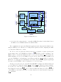
1
require large amounts of storage space (buffering, traffic description), while the SRAM is
more appropriate for time-critical operations (histograms). Depending on the application,
the two GE ports can be fully independent or data can flow from one port to the other.
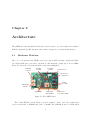
The third RJ45 port is used for clock synchronization among multiple cards (via a clock
distribution system); the PCI bus can also be used to synchronize cards in the same chassis.
The main component is the Altera Stratix FPGA, a device containing 25k logic elements.
To simplify the board layout the Ethernet MAC and PCI functionality are embedded in the
FPGA (using IP cores from MoreThanIP and PLDA respectively, [9], [10]). The firmware
contains blocks common to all projects (MAC, PCI, control) plus application dependent
parts (see Section 3.2). Most of the high-level functionality is implemented in the HandelC hardware description language [11]. All projects share a common low-level library that
provides primitives for accessing the memories, routines to simplify the creation of Ethernet
packets and a simplified PCI interface. All of the applications make heavy use of the dual-port
SRAM blocks provided by the Stratix FPGA to implement queues between concurrent and
asynchronous processes.
VHDL glue code is used in the firmware to inter-connect the various blocks (Handel-C
netlist, MAC and PCI cores, SDRAM controllers, etc); for the entire project the size of this
glue code is significant (≈2200 lines). Any design modifications would require manual changes
of the code, an error prone process. To simplify its maintenance we created a tool that takes as
input the names of the blocks and the relationships between them and generates the required
source code (VHDL Gen, [12]); this tool has saved considerable effort.
The compilation of the firmware is done using the Altera Quartus fitter. The Handel-C
compiler creates a netlist that has to be linked against the entities to which it interacts (MAC
and PCI core, SDRAM controllers, etc.). All these connections are created in the top-level
VHDL file created using VHDL Gen. The typical logic resource utilization is about 90% from
which approximatively 50% is the user code. Squeezing the required functionality into the
available resources proved to be a challenge. Multiple clock domains are used – the most
demanding being the Gigabit interface running at 125MHz. The Handel-C user code runs
normally at 41 MHz which is fast enough to keep up with the Gigabit data rates.
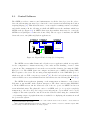
The GETB card fits into a standard 3.3V PCI slot. The PCI interface is used to configure
the application firmware, to collect statistics and to perform firmware upgrades. The large
scale testbed is built using many cards mounted in industrial PCs which are interconnected
in a local network. The typical configuration for the large scale GETB testbed is shown in
Figure 2.8 from Section 2.3. Our current setup has 128 GE ports, but there is no technical
limitation on the number of ports in the system.
7