1
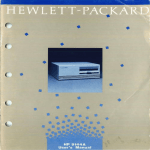
HP 9000 Series 200 Computers
Model 217
HP9817
Hardware Support Document
Flin-
HEWLETT
.:~ PACKARD
HP 9817
Hardware Support Document
for HP 9000 Series 200 Computers
Manual Reorder No. 09817-90031
© Copyright 1985 Hewlett-Packard Company
This document contains proprietary information which is protected by copyright. All rights are reserved. No part of this document may be
photocopied. reproduced or translated to another language without the prior written consent of Hewlett-Packard Company. The information
containea in this document is subject to change without notice.
Restricted Rights Legend
Use. duplication or disclosure by the Government is subject to restrictions as set forth in paragraph (b)(3)(8) of the Rights in Technical Data
and Software clause in DAR 7-104.9(a).
Hewlett-Packard Company
3404 East Harmony Road. Fort Collins. Colorado 80525
Printing History
New editions of this manual will incorporate all material updated since the previous edition. Update
packages may be issued between editions and contain replacement and additional pages to be merged
into the manual by the user. Each updated page will be indicated by a revision date at the bottom of
the page. A vertical bar in the margin indicates the changes on each page. Note that pages which are
rearranged due to changes on a previous page are not considered revised.
The manual printing date and part number indicate its current edition. The printing date changes when
a new edition is printed. (Minor corrections and updates which are incorporated at reprint do not
cause the date to change.) The manual part number changes when extensive technical changes are
incorporated.
October 1985 ... Edition 1. Replaced part number 09817-90030. Merged September 1984 update.
NOTICE
The information contained in this document is subject to change without notice.
HEWLETT-PACKARD MAKES NO WARRANTY OF ANY KIND WITH REGARD TO THIS MANUAL, INCLUDING, BUT NOT
LIMITED TO, THE IMPLIED WARRANTIES OF MERCHANTABILITY AND FITNESS FOR A PARTICULAR PURPOSE. HewlettPackard shall not be liable for errors contained herein or direct, indirect, special, incidental or consequential damages in
connection with the furnishing, performance, or use of this material.
WARRANTY
A copy of the specific warranty terms applicable to your Hewlett-Packard product and replacement parts can be obtained from
your local Sales and Service Office.
ii
iii
Table of Contents
Chapter 1: Product Description
Introduction . , . . . . . . . . . . . . . . . . . . . . . . . . . . . . . . . . . . . . . . . . . . . . . . . . . . . . . . . . . . . . . . . .. 1
Product Information ............................................................. 2
Processor, . . . . . . . . . . . . . . . . . . . . . . . . . . . . . . . . . . . . . . . . . . . . . . . . . . . . . . . . . . . . . . . .. 2
Clock and Timers . . . . . . . . . . . . . . . . . . . . . . . . . . . . . . . . . . . . . . . . . . . . . . . . . . . . . . . . . .. 2
Beepers .. , ................................................................. 2
Features ., . . . . . . . . . . . . . . . . . . . . . . . . . . . . . . . . . . . . . . . . . . . . . . . . . . . . . . . . . . . . . . . .. 3
Physical. . , . . . . . . . . . . . . . . . . . . . . . . . . . . . . . . . . . . . . . . . . . . . . . . . . . . . . . . . . . . . . . . . .. 3
Power Requirernents ......................................................... 3
Product Configuration. . . . . . . . . . . . . . . . . . . . . . . . . . . . . . . . . . . . . . . . . . . . . . . . . . . . . . . . . .. 4
Custorner Service Support. . . . . . . . . . . . . . . . . . . . . . . . . . . . . . . . . . . . . . . . . . . . . . . . . . . . . .. 5
On··site Repair .............................................................. 5
Service Center Repair. . . . . . . . . . . . . . . . . . . . . . . . . . . . . . . . . . . . . . . . . . . . . . . . . . . . . . .. 5
Customer Repair. . . . . . . . . . . . . . . . . . . . . . . . . . . . . . . . . . . . . . . . . . . . . . . . . . . . . . . . . . .. 5
Backplane Power Limits. . . . . . . . . . . . . . . . . . . . . . . . . . . . . . . . . . . . . . . . . . . . . . . . . . . . . . . .. 7
User Documentation . . . . . . . . . . . . . . . . . . . . . . . . . . . . . . . . . . . . . . . . . . . . . . . . . . . . . . . . . . .. 9
BA~3IC ... " ............................................................... '.. 9
Pascal .................................................................... 9
Service Documentation. . . . . . . . . . . . . . . . . . . . . . . . . . . . . . . . . . . . . . . . . . . . . . . . . . . . . . . . .. 9
Miscellaneous. . . . . . . . . . . . . . . . . . . . . . . . . . . . . . . . . . . . . . . . . . . . . . . . . . . . . . . . . . . . .. 10
Chapter 2: Site Preparation and Requirements
Site Preparation. . . . . . . . . . . . . . . . . . . . . . . . . . . . . . . . . . . . . . . . . . . . . . . . . . . . . . . . . . . . . ..
Class B Specifications. . . . . . . . . . . . . . . . . . . . . . . . . . . . . . . . . . . . . . . . . . . . . . . . . . . . . . . . ..
Temperature . . . . . . . . . . . . . . . . . . . . . . . . . . . . . . . . . . . . . . . . . . . . . . . . . . . . . . . . . . . . ..
HUlnidity .................................................................
Vibration. . . . . . . . . . . . . . . . . . . . . . . . . . . . . . . . . . . . . . . . . . . . . . . . . . . . . . . . . . . . . . . . ..
Shock (non-operating) . . . . . . . . . . . . . . . . . . . . . . . . . . . . . . . . . . . . . . . . . . . . . . . . . . . . ..
Altitude. . . . . . . . . . . . . . . . . . . . . . . . . . . . . . . . . . . . . . . . . . . . . . . . . . . . . . . . . . . . . . . . . ..
Transportation .............................................................
Power Hequirements ...........................................................
11
11
11
11
12
12
12
12
13
Chapter 3: Installation and Configuration . .......................................... 15
Chapter 4: Preventive Maintenance
Cleaning. " " " " .. " .................................................... " ... " . . .. 1 7
Chapter 5: Functional Description
Introduction . . . . . . . . . . . . . . . . . . . . . . . . . . . . . . . . . . . . . . . . . . . . . . . . . . . . . . . . . . . . . . . . ..
Processor Board. . . . . . . . . . . . . . . . . . . . . . . . . . . . . . . . . . . . . . . . . . . . . . . . . . . . . . . . . . . . . ..
110 Connectorboard ...........................................................
Power ~3upply .................................................................
19
19
21
21
iv
Chapter 6: Removal and Replacement
Introduction . . . . . . . . . . . . . . . . . . . . . . . . . . . . . . . . . . . . . . . . . . . . . . . . . . . . . . . . . . . . . . . . ..
Top Cover Removal . . . . . . . . . . . . . . . . . . . . . . . . . . . . . . . . . . . . . . . . . . . . . . . . . . . . . . . . . ..
Front Panel Removal. ..........................................................
Power Supply Removal . . . . . . . . . . . . . . . . . . . . . . . . . . . . . . . . . . . . . . . . . . . . . . . . . . . . . . ..
Rear Panel Removal . . . . . . . . . . . . . . . . . . . . . . . . . . . . . . . . . . . . . . . . . . . . . . . . . . . . . . . . . ..
Processor Board Removal . . . . . . . . . . . . . . . . . . . . . . . . . . . . . . . . . . . . . . . . . . . . . . . . . . . . ..
110 Connectorboard Removal . . . . . . . . . . . . . . . . . . . . . . . . . . . . . . . . . . . . . . . . . . . . . . . . . ..
Power Receptacle Removal . . . . . . . . . . . . . . . . . . . . . . . . . . . . . . . . . . . . . . . . . . . . . . . . . . . ..
25
29
31
32
34
35
36
38
Chapter 7: Adjustments ........................................................... 41
Chapter 8: Troubleshooting and Diagnostics
Introduction . . . . . . . . . . . . . . . . . . . . . . . . . . . . . . . . . . . . . . . . . . . . . . . . . . . . . . . . . . . . . . . . ..
Initial Troubleshooting Procedure . . . . . . . . . . . . . . . . . . . . . . . . . . . . . . . . . . . . . . . . . . . . . . ..
Dead Unit Procedure ...........................................................
Power Supply . . . . . . . . . . . . . . . . . . . . . . . . . . . . . . . . . . . . . . . . . . . . . . . . . . . . . . . . . . . ..
Troubleshooting a Dead Unit. ................................................
Power Supply Voltage Check ................................................
Live Unit Procedure . . . . . . . . . . . . . . . . . . . . . . . . . . . . . . . . . . . . . . . . . . . . . . . . . . . . . . . . . ..
Turn-on Self-test ..............................................................
Self-test Sequence ..........................................................
Running the Self-test . . . . . . . . . . . . . . . . . . . . . . . . . . . . . . . . . . . . . . . . . . . . . . . . . . . . . ..
Boot ROM Beeper Codes ...................................................
Processor Test . . . . . . . . . . . . . . . . . . . . . . . . . . . . . . . . . . . . . . . . . . . . . . . . . . . . . . . . . . . . . . ..
Processor Test. . . . . . . . . . . . . . . . . . . . . . . . . . . . . . . . . . . . . . . . . . . . . . . . . . . . . . . . . . . ..
Boot ROM Memory Test. . . . . . . . . . . . . . . . . . . . . . . . . . . . . . . . . . . . . . . . . . . . . . . . . . . . . . ..
Boot ROM Test. . . . . . . . . . . . . . . . . . . . . . . . . . . . . . . . . . . . . . . . . . . . . . . . . . . . . . . . . . ..
RAM Memory Tests. . . . . . . . . . . . . . . . . . . . . . . . . . . . . . . . . . . . . . . . . . . . . . . . . . . . . . . . . . ..
Top RAM Test .............................................................
RAM Pattern Test . . . . . . . . . . . . . . . . . . . . . . . . . . . . . . . . . . . . . . . . . . . . . . . . . . . . . . . . ..
RAM Addressing. . . . . . . . . . . . . . . . . . . . . . . . . . . . . . . . . . . . . . . . . . . . . . . . . . . . . . . . . ..
Checking a 1M Byte RAM Card Address .......................................
Checking a 256K Byte RAM Card Address. . . . . . . . . . . . . . . . . . . . . . . . . . . . . . . . . . . ..
Locating a Defective RAM Block. . . . . . . . . . . . . . . . . . . . . . . . . . . . . . . . . . . . . . . . . . . . ..
Keyboard Test . . . . . . . . . . . . . . . . . . . . . . . . . . . . . . . . . . . . . . . . . . . . . . . . . . . . . . . . . . . . . . ..
Keyboard Test. . . . . . . . . . . . . . . . . . . . . . . . . . . . . . . . . . . . . . . . . . . . . . . . . . . . . . . . . . . ..
I/O Tests . . . . . . . . . . . . . . . . . . . . . . . . . . . . . . . . . . . . . . . . . . . . . . . . . . . . . . . . . . . . . . . . . . . ..
43
44
50
50
51
54
55
58
59
60
62
62
62
63
63
64
64
64
64
65
65
66
67
67
68
Chapter 9: Replacement Parts
Introduction . . . . . . . . . . . . . . . . . . . . . . . . . . . . . . . . . . . . . . . . . . . . . . . . . . . . . . . . . . . . . . . . .. 69
Chapter 10: Reference
Boot ROM Error Codes . . . . . . . . . . . . . . . . . . . . . . . . . . . . . . . . . . . . . . . . . . . . . . . . . . . . . . .. 75
v
Chapter 11: Product History
IntrodLlction . . . . .. . . . . . . . . . . . . . . . . . . . . . . . . . . . . . . . . . . . . . . . . . . . . . . . . . . . . . . . . . . .. 77
Chapter 12: Diagrams
Figure 12-1. Block Diagram ....... -..............................................
Figure 12-2. Power Distribution Diagram ..........................................
Figure 12-3. Initial Troubleshooting Flowchart ......................................
Figure 12-4. Dead Unit Troubleshooting Flowchart . . . . . . . . . . . . . . . . . . . . . . . . . . . . . . . ..
Figure 12-5. Live Unit Troubleshooting Flowchart ..................................
Figure 12-6. Computer Assembly Locations . . . . . . . . . . . . . . . . . . . . . . . . . . . . . . . . . . . . . ..
79
80
81
82
83
85
vi
1
Chapter
Product Description
1
Introduction
This manual contains all the servicing information for the HP Series 9000 Model 21 7 computer.
The Model 217 computer is referred to interchangeably by its product number, by HP 9817, or by
the term "computer". All three forms refer to the Model 217.
Hewlett-Pi:lckard supports repairing HP 9817 computers to the assembly level only, that is, isolating
the problem to an assembly such as the processor board. Then the defective assembly is exchanged
for a new or rebuilt assembly.
Also included in this chapter is service support information and a list of the documentation available
for HP 981 7 computers.
Additional information in this manual includes:
• Site Preparation
• Installation and Configuration
• Preventive Maintenance
• Functional Description
• Troubleshooting and Diagnostics
• Adjustments
• Removal and Replacement
• Replacement Parts
• Reference Material
• Product History
2 Product Description
Product Information
The HP 9000 Model 217 computer is a small, modular, MC68010-based computer. Modular refers
to the fact that it is composed of a group of "modules", such as the keyboard, the display or the
central processing unit. The MC68010 is fully object code-compatible with the MC68000, but has
the added features of virtual memory support and enhanced execution timing.
It has these specifications:
Processor
Type:
Motorola 68010
Clock frequency:
8 MHz
Internal architecture:
32-bit data and address registers
Address range:
16M bytes
Data bus:
16-bit asynchronous
Instruction types:
57
Major data types:
5
Addressing modes:
14
Interrupt levels:
6 maskable and 1 non-maskable
Clock and Timers
Real-time clock
Resolution:
10 msec
Accuracy:
50 ppm (4.3 sec/day)
Power-on default:
Midnight, January 1
Timers
Delay interrupt:
10 msecs to 1.94 days in 10 msec increments
Cycled interrupt:
10 msecs to 1.94 days in 10 msec increments
Match interrupt:
Match on time of day, 0.00 to 84600.00 seconds (23.5 hours)
Beepers
Range (nominal):
81.375 Hz to 5208 Hz
Duration:
.01 to 2.55 sec
Beeper hardware supports three tone generators with attenuators and white noise source.
Product Description
Features
• HP stc:mdard industrial package
• Six accessory card slots (three for external interface cards)
• Pascal 3.0 and BA.SIC 3.0 language systems
• Supports external 14-inch medium-resolution, monochrome display (35721A/B/C)
• HP-HIL keyboard support (46020A)
Physical
Height:
130 mm (5.12 inches)
Width:
325 mm (12.80 inches)
Depth:
285 mm (11.22 inches)
Net weight:
6 kg (13.2 pounds)
Shipping weight:
9.5 kg (20.9 pounds)
Power Requirements
Operating voltage:
90 to 125 Vac, 198 to 250 Vac switch-selectable
Operating frequency:
48 to 66 Hz
Power consumption:
130 W (maximum)
Accessory slot power:
41.25 W@ +5 V
18.70 W @ + 12 V
6.00 W C~ -12 V
The accessory slot + 5 V lines are fuse-limited to 25 W for each pair of slots.
3
4 Product Description
Product Configuration
The Model 217 is available in two configurations, the modular computer only (9817A) or a
complete hardware system (9817H).
Product
Number
Description
9817A
Model 217 Computer
.~ Built-in HP-IB interface with 2 m cable
.~ Built-in RS-232 interface (order cable separately)
i' 6 accessory slots for interfaces, language systems and memory
.~ Built-in HP-HIL interface
9817H
Model 217 Computer
.~ Built-in HP-IB interface with 2 m cable
.~ Built-in RS-232 interface (order cable separately)
* 6 accessory slots for interfaces, language systems and memory
* Built-in HP-HIL interface
512K bytes of RAM memory (two 98256A cards)
46020A keyboard
35721A, B or C 14·inch monochrome monitor
98204B video interface
35722A tilt and swivel unit
Option 001: 1M byte RAM memory (one 98257A substituted for two 98256A cards)
Product Description
Customer Service Support
Hewlett-Packard provides service support in three ways: on-site repair, service center repair and
customer repair.
On-site Repair
For on-site repair, an HP Customer Engineer goes to the customer's site and troubleshoots and
repairs the computer at the assembly level. The defective assembly is then exchanged for a new or
reconditioned assembly. This is the fastest way to get the computer up and running. Consult your
HP Sales and Service office for turnaround times.
Service Center Repair
For service center repair, the customer returns the defective computer to an HP Field Repair
Center. An HP Service Technician repairs the computer and returns it to the customerl. Table 1-1
contains a list of the Field Repair Centers. Consult your HP Sales and Service office for turnaround
times.
Customer Repair
Customers have the option of repairing their own computers. Contact your nearest HP Sales/
Service office for information concerning recommended spare assemblies and training.
INTERCONTINENTAL
HONG KONG
MEXICO
ARGENTINA
HONG KONG
MEXICO CITY
BUENOS AIRES
Hewlett-Packard Hong Kong Ltd.
5 Floor Sun Ilung Kai Centre
30 HMbour Road
Wanchai,
Phone: 5/H32-3211
Hewlett-Packard Mexicana SACV
Avenida Periferico Sur h50l
Col. Tepepan, Xochirnilco
Mexico City, DFlh020
Phone: 905/67h-4600
Hewlett-Packard Argentina S. A.
Avda Santa Fe 2035
Martlne/, 1h40
Phone 792-1291
AUSTRALIA
New South Wales
SYDNEY
Hewlett·Packard Australia Ltd.
17-23 1;1 LIVl'ra Ruad
North Rvdl', New South Wales 211.1
Phone: 02 IHH7-lhl 1
Victoria
JAPAN
SINGAPORE
Kanagawa
SINGAPORE
SAGAMIHARA
Hewlett-Packard Singapore Ltd.
6th Floor, Inchcape House
450-452 Alexandra Road
Singapore, 0511
Phone: 5/h31-7HH
Yokogawa Hewlett-Packard
1-27-15 'tabe
Sagarnihara, Kanagawa 229
Phone: 427/59-1311
Osaka-Shi
OSAKA
MELBOURNE
Hewlett-Packard Australia Ltd.
., 1-41 Joseph Street
Blackburn, Victoria 3130
I'honL': 0.1 IH90-h35 I
Yokogawa-Hewlett-Packard Ltd.
Chuo Bldg. NishinakaJirna
5-4-20, Yodogawa-ku
Osaka, Osaka-Shi 532
Phone: h 1304-h021
BRAZIL
Suginami-ku
SAO PAULO
TOKYO
Hewlett-Packard Brasil I.e.C
AlalT1l'dd Rio Negro 750
Alphaville
HarUl'ri, SP-0h400
Phone 011!421-1311
Yokogawa-Hewlett-Packard Ltd.
3-29-21 Takaido-Higashi
Tokyo, Suginarni-ku IhH
Phone: 31331 -h 111
TAIWAN
TAIPEI
Hewlett-Packard Far East Ltd.
Bank Tower, 5th Floor
205 Tun Hwa North Road
Taipei,
Phone: 2/751-0404
VENEZUELA
CARACAS
Hewlett-Packard Venezuela CA.
Edificio Segre 2Y3
3a Transversal Los Ruices Nort
Caracas, 1071
Phone: 2 1239-4133
Figure 1-1. Field Repair Centers
5
6 Product Description
NORTH AMERICA
Maryland
BELGIUM
NORWAY
CANADA
WASHINGTON D.C.
BRUSSELS
OSLO
Hewlett-Packard Company
Hewlett-Packard Belgium SA/NY
Hewlett-Packard Norge AJS
2 Choke Cherry Road
Rockville, Maryland 20H50
Phone: 3111IY48-6370
Boukvard de la Woluwe 100
Woluwedal lOll
Brussl'ls B-120{)
I'ho'~e: 1762-320{)
Ol'sterudall'n 18
Ol'steraas, N- 1]45
I'hone:2/17-11-80
Alberta
EDMONTON
Hewlett-Pack.ud Canada Ltd.
11620A 16Hth Street
Edmonton, Alberta T5M ,nY
Phone: -+03/-+52-3670
British Columbia
VANCOUVER
Hewlett-Packard Canada Ltd.
lO6YI Shellbrid~l' W.ly
Richmond, Brtllsh Columbia
V6X 2WH
Phol1l': 604/270-2277
Ontario
TORONTO WEST
Hewlett-Packard Canada Ltd.
6H77 Goreway Drive
Mississauga, Ontario 14V IMH
Phone: -+16/67H-Y430
UNITED STATES
California
LOS ANGELES WEST
Massachusetts
BOSTON
Hewlett-Packard Company
32 Hartwell Avenue
Lexinghln, Massachusetts ()2173
Phone: hI7/H61-H%0
Michigan
DETROIT
Hewlett-Packard Company
3%50 Orchard Hill Drive
Novi, Michigan 4H050
Phone: 3 1Ji349-Y200
New Jersey
PARAMUS
Hewlett-Packard Company
WI20 Cl'ntury Road
Paramu~, New jl'rsl'y 07652
Phone: 2111l265-5000
Pennsy Ivania
Hewlett-Packard Company
PHILADELPHIA
5-+00 W, Rosecrans Blv'I.
Lawndall', California Y0260
Phone: 21J/M3-7500
Hewlett-Packard Company
SANTA CLARA
Hewlett-Packard Company
Valley Forge Corporate Center
2750 Monroe Boulevard
Valley FI 1r,8e, Pennsylvania IY4H2
Phone: 2 b/265-7000
3003 Scott Boukvard
Santa Clara, California 951150
Phone: 40H/988-70()O
Texas
Colorado
930 East Campbl'll Road
Rlchard~on, Tex,ls 750HI
Phone: 214/231-6101
DENVER
Hewlett-Packard Company
24 Inverness Place, Ea~t
Englewood, Colorado ~0112
Phone: 303 1771-3455
Georgia
ATLANTA
DALLAS
Hewlett-Packard Company
Washington
SEATTLE
Hewlett-Packard Company
I'iHI5 S, I ,37th Street
Bellevue, Washington YHO()6
Phone 211hl643--+000
Hewlett-Packard Company
2000 South Park Place
Atlanta, C;eor~ia 3OJ3Y
Phone: -+04/Y5:->-1500
Illinois
CHICAGO WEST
Hewlett-Packard Company
'i2l)] Tolh'iew Drive
Rolling Meadows, Illinlli~ hO()OH
Phone 3122'i'i-YHOO
EUROPE AND
MIDDLE EAST
AUSTRIA
VIENNA
Hewlett-Packard GmbH
Lieblga~~e I
I'o~tfach 72
Vil'l1na, ,\-1222
Phone 222 3'i Ih210
i
DENMARK
COPENHAGEN
Hewlett-Packard A/S
Datavej 52
Birkerlled, DK-346ll
Phone: 2 IH l-hh-40
FINLAND
HELSINKI
Hewlett-Packard Oy
Revontulentie 7
Espoo, SF-02100
Phone: 90/455-0211
SOUTH AFRICA
Transvaal
JOHANNESBURG
Hewlett-Packard South Africa
Private Bag
Wendywood
Sandton, Transvaal 2144
Phone: 1\ 1802-51\
SPAIN
MADRID
Hewlett-Packard Espanola S.A.
Hewlett-Packard Oy
Costa Brava, 13-2
Mirasierra
Madrid, E-34
Phone: 91/734-1162
Vainonkatu 9c
Jyvaskyla, SF-411100
Phone: 41 121h31H
STOCKHOLM
JYVASKYLA
OULU
Hewlet-Packard Oy
Kainuuntieic
Oulu, SF-YOI40
Phone: HI 1338785
FRANCE
ORSAY
Hewlett-Packard France
Les Ulis Avenue De TropiLJues
Z. Industridlc de Courtaboeuf
Les Ulis, F-YIY47
(,hol1l': h 19077825
SWEDEN
Hewlett-Packard Sverige AB
SkalhoItsgatan 9, Kista
Box 19
Spanga, 5-16393
Phone: 81750-2000
SWITZERLAND
ZUERICH
Hewlett-Packard (schweiz) AG
allmend 2
Widen, CH-8Yh7
Phone: 571312111
UNITED KINGDOM
GERMANY
ENGLAND
BOEBLINGEN
MANCHESTER
Hewlett-Packard GmbH
Herrenberger Strasse I III
BI1l'blingen, D-7030
Phone: 7031hh7750
ITALY
Hewlett-Packard Ltd.
Trafalgar Ilouse
Navigation Road
Altrincham, England WAI4 INU
I'hone: hI IY28-6422
MILANO
WINNERSH
Hewlett-Packard Italiana S.p.A
Hewlett-Packard Ltd.
Via C, Oi Vittorio Y
Cl'rnllsco Sui Navigl, 1-200h3
Phone 2 ;YOJhY 1
NETHERLANDS
AMSTELVEEN
Hewlett-Packard Nederland B. V.
Van Hellven Coedhartlaan 121
Amstdveen, NL-118IKK
Phon!': 20 i472()21
Figure 1-1. Field Repair Centers (Cont.)
King Stred Lane
Winnersh
Wokingham, England RC II SAR
Phone: 734/784-774
Product Description
Backplane Power Limits
The limits for the backplane power available to accessories is not to be exceeded by the installed
accessories. To help determine the power requirements of a particular set of accessories, the
following power requirements for accessories are listed.
CAUTION
IF THE POWER REQUIRED FOR ACCESSORIES EXCEEDS THE
POWER AVAILABLE AT THE COMPUTER BACKPLANE, DAMAC;E
TO THE COMPUTER'S POWER SUPPLY AND/OR THE ACCESSORY WILL OCCUR. HEWLETT -PACKARD DOES NOT SUPPORT
ACCESSORY CONFIGURATIONS REQUIRING MORE POWER
THAN IS RECOMMENDED AT THE COMPUTER BACKPLANE.
To detern1ine the sUitability of a given set of accessories for your computer, follow these instructions:
1. Calculate the accessory power required for each supply voltage and the total power required
for the accessory using the information in Table 1-2. Enter these values in the "Total Power
Required" block in Table I-I.
2. If the total pOWE~r required is greater than 56.26 W, or the power drawn at any given voltage
exceeds the value for that level, you must:
a. Change the type/number of accessories,
b. Add an HP 9888A Expander, or
3. Recalculate the power required versus power available.
Table 1-1. Power Requirements Calculation Table
Power Supply Voltage
+5
+12
-12
Backplane
Maximum
48.5 W
9.12W
5.04W
56.26 W
accessory 1
accessory 2
accessory 3
accessorY 4
accessory 5
accessory 6
Total power required
HP 9817 power available
7
8 Product Description
Table 1-2. Typical Power Requirements for Series 200 Accessories
Power Requirements
Product
HP 9888A
HP 13264A
HP 13265A
HP 13266A
HP 98028A
HP 98204B
HP 98204B
HP 98253A
HP 98254A
HP 98255A
HP 98256A
HP 98257A
HP 98259A
HP 98601A
HP 98601A
HP 98602A
HP 98604A
HP 98620A
HP 98621A
HP 98622A
HP 98623A
HP 98624A
HP 98625A
HP 98626A
HP 98627A
HP 98628A
HP 98629A
HP 98629A
HP 98630A
HP 98635A
HP 98640A
HP 98644A
HP 98691A
Description
Bus Expander
Data link Pod
Modem
Current Loop Pod
Res. Mgmt. MUX
Video wlo Graph.
Video w/Graphics
EPROM Prog.
64K byte RAM
EPROM Card
256K byte RAM
1M byte RAM
128K byte Bubble
BASIC 2.0 ROM
BASIC 1.0 ROM
BASIC 2.1 ROM
HPL 2.0 ROM
DMA Controller
BASIC 1.0 Opt. 1
GPIO Interface
BCD Interface
HP-IB Interface
Disc Interface
RS-232 Interface
Color Interface
Datacomm Interf.
Resource Mgmt. wlo 98028A
Resource Mgmt. w/98028A
Breadboard Card
Floating-Point
A-D Card
Serial Load Card
Progr. Datacomm
+5
5.0
0.2
0.5
1.0
2.2
7.5
15.0
5.7
3.0
2.8
4.1
6.0
2.4
2.4
2.3
3.6
1.5
6.0
2.3
3.8
2.5
2.4
3.0
2.0
5.5
3.6
3.7
5.9
1.3
4.2
1.0
2.0
6.4
+12
-12
1.9
0.5
1.0
6.4
0.3
0.5
1.0
2.9
0.1
0.6
0.6
0.5
0.5
6.9
0.7
0.5
0.5
0.7
0.3
2.0
0.6
0.02
1.3
Total
5.0
2.4
1.5
3.0
8.6
7.5
15.0
5.7
3.0
2.8
4.1
6.0
5.3
2.4
2.3
3.6
1.5
6.0
2.3
3.8
2.5
2.4
3.1
3.2
5.5
4.8
4.7
13.3
1.3
4.2
2.3
2.3
9.7
Product Description
User Documentation
BASIC Manual
Manual
Part Number
98613-10010
98613-87901
98613-10020
98613-10030
98613-90010
98613-90020
98613-90030
98613-90040
98613-90050
98613-90060
98613-90070
Description
CSUB Preparation Manual
BASIC 3.0 Manual Kit contains one each of the following manuals:
Utilities library Manual
Loader Utility Manual
BASIC 3.0 Programming Techniques
BASIC 3.0 Interfacing Techniques
BASIC 3.0 Graphics Techniques
BASIC 3.0 User's Guide
BASIC 3.0 Language Reference
Condensed Reference
Documentation Guide and Master Index
Pascal
Manual
Part NUinber
98615-87902
09826-90072
09826-90073
98615-90021
98615-90030
98615-90035
98615-90040
98615-9()050
Description
Pascal 3.0 Manual Kit contains one each of the following manuals:
Pascal Textbook (Wiley)
MC68000 User's Manual
Pascal 3.0 Workstation System
Pascal 3.0 Procedure library
Pascal 3.0 Graphics Techniques
Pascal 3.0 User's Guide
HP Pascal Language Reference for Series 200 Computers
Service Documentation
Manual
Part Number
09817 -90030
09817 -90039
09817 + 49A-90101
35 7~~ 1-90()04
Description
HP 9817 Hardware Support Document
HP 9817 CE Handbook Section
Model 217 Self-Paced Hardware Training Guide
HP 35721A/B/C Service Manual
9
10 Product Description
Miscellaneous
Manual
Part Number
98204~90001
98257-90000
98620-90001
98622-90000
98623-90000
98624-90000
98625-90000
98626-90000
98627 -90000
98628-90001
98630-90000
98635-90000
Description
HP 98204B Composite Video Card Installation Note
HP 98257 A RAM Card Installation Note
HP 98620A/B DMA Card Installation Note
GPIO Installation Manual
BCD Installation Note
HP-IB Installation Note
Disc Interface Installation Manual
RS-232 Installation Manual
Color Video Interface Installation Manual
HP 98628198691 Datacomm Installation Manual
HP 98630A Breadboard Installation Manual
HP 98635A Floating-Point Math Card Installation Note
11
Chapter
Site Preparation and Requirements
2
Site Preparation
Site preparation requirements for the HP 9817 computer are:
Environmental Class B or higher: No site prep needed
Othen.vise: Upgrade site to Class B
Class B Specifications
Class B specifications are designed for commercial and industrial environments, that is, light or
medium industrial and commercial manufacturing facilities suitable for occupancy by operating
personnel on a full-time basis without benefit of air conditioning or other protective measures.
This kind of environment is expected to fall within the specifications in Table 2-1. If any parameter
falls outside the specification, steps must be taken to ensure that the computer is sUitably protected.
Table 2-1. Class B Specifications
Temperature
Non -operating
-40 to + 75°C
Operating Survival
-20 to +65°C
Operating
o to
+55°C
Humidity
Non -opera ting
90% R.H. @ 65°C
Operating
o to 95% R.H.
Supersoak
24 Hours
Condensation
Operates without damage and recovers within specified time limits
@ 40°C
Vibration
Cycle Range
5 to 55 to 5 Hz
Amplitude (p-p)
0.38mm
SweeptimE~
1 min./octave, 15 min. total
Dwell at Resonances
10 min. each resonance
Amplitude at Resonances
5 to 10 Hz
3.17 mm
10 to 25 Hz
1.52 mm
25 to 55 Hz
.38mm
12
Site Preparation and Requirements
Table 2.1. Class B Specifications (cont.)
Shock (non-operating)
Magnitude
30g
Duration
11 ms
'Number of Shocks
18
Waveform
Half-sine
Bench Handling
102 mm Tilt Drop
Altitude
Non-operating
15300 m
Operating
4600m
Transportation
Drop Test (in shipping carton) 752 mm
Site Preparation and Requirements
Power Requirements
Power requirements for the HP 9817 computer are:
Power:
130W
Voltage:
90 to 125 or 198 to 250 Vac
Frequency:
48 to 66 Hz
13
14 Site Preparation and Requirements
15
~nstallatiOn and Configuration
Chapter
3
This chapter is composed of the following installation documentation:
09817-90000
Model 217 Installation Guide
98257-90000
98256A and 98257 A Installation Note
98204-90001
982048 Composite Video Interface Inst. Note
These documents are supplied with the HP 9817 Service Manual Kit. If you purchased this kit,
place these documents after this page.
16
Installation and Configuration
17
L
Chapter
Preventive Maintenance
4
There is no preventive maintenance for the HP 9817 computer, other than cleaning.
Cleaning
To preserve the appearance of the computer, follow these instructions:
Unplug the power cord and remove any interconnecting cables. Dampen a clean, soft, lint-free
cloth with a solution of clean water and mild soap. Wipe the soiled areas, ensuring that no cleaning
solution gets inside. Then dry with a clean, soft, lint-free cloth.
CAUTION
CHEMICAL SPRAY -ON CLEANERS USED FOR APPLIANCES AND
OTHER HOUSEHOLD APPLICATIONS MAY DAMAGE THE FINISH. THESE AND OTHER CHEMICAL CLEANERS SHOULD NOT
BE USED. THE COMPUTER SHOULD BE CLEANED WITH CLEAN
WATER AND MILD SOAP ONLY.
18
Preventive Maintenance
19
Chapter
Functional Description
5
Introduction
This chapter describes the function of the assemblies in the HP 981 7 computer. The functional
description may be easier to follow if you locate the various components on the block diagram,
Figure 5-3.
The HP 981 7 consists of these functional units:
• Processor board
• I/O connectorboard
• Power supply
The function of these units is as follows:
Processor Board
The processor board consists of two distinct sections, the processor section and the input/output
section.
The processor section contains the CPU, a memory management unit, a programmable timer
module, a system configuration register, a power-up configuration register, self test LEDs and
control circuitry buffers.
The CPU is a Motorola MC68010 microprocessor, with 32-bit data and address registers, 16
megabyte direct addreSSing range, 57 instruction types and memory-mapped I/O. The CPU controls a bus with 23 address lines, 16 data lines and 17 control lines. Control signals allow asynchronous communication with a variety of memory and I/O devices, and allow for different bus masters,
interrupt operation, and selective byte or word addreSSing.
The memory managernent unit provides virtual memory capabilities to the computer. The programmable timer module provides periodic interrupts to the CPU for multi-tasking purposes.
The systen1 configuration register is a PROM which contains information about the configuration of
the system as well as the machine serial number. The power-up configuration register is a switch
block which allows the user to define a power-up configuration for the software. The eight self-test
LEDs report the status of the self-test and any errors encountered by it.
The input/output (1/0) section of the processor board contains the boot ROM, a keyboard and
speaker interface, an HP-IB interface and an RS-232 interface.
20
Functional Description
The boot ROM contains 48K bytes of software instructions. These are the first instructions executed
by the CPU at start-up, and serve to initialize the 9817, run the turn-on 'self-test and load the
language system.
The keyboard and speaker interface consists of an 8042A keyboard controller IC, an HP-HIL
(Hewlett-Packard Human Interface Loop) controller, a 76494 tone generator and a speaker driver.
The keyboard controller provides a system interface to the HP-HIL controller and to the tone
generator, as well as system timer functions. The tone generator consists of three programmable
tone generators and a programmable noise source. It produces an analog audio signal to the
speaker driver. The speaker driver is an audio amplifier and produces a signal capable of driving the
speaker mounted on the chassis. The HP-HIL controller provides an interface between the
keyboard controller and the loop, and handles all HP-HIL external protocol. The loop is a fourwire, serial daisy chain, consisting of input devices such as a keyboard, joystick or mouse.
The built-in HP-IB interface contains all the circuitry required to communicate via an HP-IB cable.
Direct Memory Access (DMA) support electronics is included, so that DMA via HP-IB is possible if a
DMA card is installed in an accessory slot.
The built-in RS-232 interface contains all the circuitry required to communicate via an RS-232
cable. It operates on a dedicated 2.4576 MHz clock.
The input/output section contains switch blocks for selecting RS-232 baud rate, remote terminal,
handshake, parity options, parity enable, number of stop bits, character length and control line
defeat.
The chip select decodes buffered address lines BA16 thru BA23 into chip select signals for the
internal HP-IB interface, the internal RS-232 interface and the keyboard.
The processor board contains switches for selecting HP-IB system controller, short or long memory
test and continuous self-test.
Functional Description
1/0 Connectorboard
The 110 connectorboard contains six accessory slots for adding RAM cards, a DMA controller card,
a floating-point math card or for interface cards used for connecting peripherals.
Each two connectors are protected by a fuse on the + 5V line. These fuses are mounted on the
connectorboard, along with a fuse protecting the processor board.
The power supply post-regulators are mounted on the 110 connectorboard.
Power Supply
The function of the power supply is to change line voltage into filtered, regulated dc levels of + 5 V,
+ 12 Vand -- 12 V. Overvoltage protection is provided on the + 5 V line. Overcurrent protection is
provided on the + 12 and -12 V lines.
The power supply consists of these assemblies:
• ac input hardware
• power supply module
• post-regulators
• fan
Ac power enters throu~3h the ac socket on the rear panel. The socket contains a fuse and a voltage
select switch which selects between 90-125 and 198-250 Vac. The ac passes to the power supply
module, which rectifies it to de. The power supply module is a sWitching supply, and produces
regulated + 5 Vdc and unregulated + 14 and -14 Vde. Post-regulators physically mounted on the
110 connectorboard convert the + 14 Vdc to + 12 Vdc and the -14 Vdc to -12Vdc.
The fan operates on the + 5 and -- 14 V lines.
Figure 5-1 is a diagram of the distribution paths for ac and dc power.
21
22
Functional Description
Address Information
Decimal Approx.
-.......--16M-1
Hex
FFFFFF
Ram
16M Bytes
900000
9M
TestlMonitor
800000
8M
External 1/0
600000
6M
Internal 1/0
400000
4M
System ROM
003FFF
256K
1K
o
Memory -
Mapped 1/0
Boots
Exception Table
23 22 21
External
1/0
600000
20 19 18 17 16
1514 13 12 1110 9 8 7 6 5 4 3 2 1
Select Code
0-31
1/0 Register Select
Standard Select Codes
Internal
Internal
1/0
4M
000000
External
Address Format:
8M r--------------,800000
6M
000400
400000
0
1
2
3
4
5
Not Used
CRT Alpha
KYBD & ClK
Graphics
Flex-Disc
6
DMA
HPIB
7
External
HPIB
RS232
10
11
12
13
14
20
DataComm
BCD
GPIO
Disc Intrlc.
31-
Figure 5-1. HP 9817 Memory Map
Functional Description
Power
Connection
Power Supply
Address
Bus
9lIIlJ ~
-
CPU
ac
Fan
Da1a Bus
>~
J2 Pin
+14V
-14V
+5V
6
8
1
Black
I/O Connectorboard
To Keyboard
I
1
I Regulator 1 l Regulator 1
Red
F4
'V
J.?...,
-12V
+-12V
F2
~
~?
-
J1 Pin
1C
1A
1
Processor Board
• Speaker, Front
Panel LED
2C
Processor
Board
10
11
Slots
(2 per
fuse)
F1
Keyboard
Connector
RS-232
Connector
'/0
~
1/0 Slots
36
Pin
Figure 5-2. Power Distribution Diagram
110 Connectorboard
Figure 5-3. HP 9817 Block Diagram
23
24
Functional Description
25
Removal and Replacement
Chapter
6
Introduction
This chapter describes how to access and remove the various assemblies from the HP 9817
computer, and how to reassemble it.
Where necessary. photographs show the assembly being removed. To reassemble the computer,
reverse the removal procedure. Some procedures are given as an aid in reassembly.
Table 6-1 lists all the major assemblies and printed circuit boards in the computer. Figure 6-1 shows
these major assemblies.
Table 6-1. Computer Configuration Chart
Description
Processor Board
Connector board
Power Supply
256K byte RAM Card
Kevboard
Video Interface
Monitor
HP 9817A
HP 9817H
09817-66511
09817-66563
09817-66552
none
none
none
none
09817-66511
09817-66563
09817 -66552
98256-66524
HP 46020A
HP 98204B
HP 35721A
HP 35721B
HP 35721C
none
98257-66524
Optional Assemblies
1M byte RAM Card
26
Removal and Replacement
Removal a n d Replacement
Top Shroud
Top Cover
(Early Production)
Top Plate
Power Socket
Fuse,
.
Voltage Select
Speaker
1/0 Connectorboard
.
Figure 6-1 . Computer Assembly Locahons
27
28
Removal and Replacement
WARNING
REMOVE ALL AC POWER TO THE COMPUTER BEFORE REMOVING ANY ASSEMBLY.
CAUTION
INTEGRATED CIRCUITS CAN BE DAMAGED BY ELECTROSTATIC DISCHARGE. USE THE FOLLOWING PRECAUTIONS:
DO NOT WEAR CLOTHING SUBJECT TO STATIC CHARGE BUILDUP. SUCH AS WOOL OR SYNTHETIC MATERIALS.
DO NOT HANDLE INTEGRATED CIRCUITS IN CARPETED AREAS.
DO NOT REMOVE AN INTEGRATED CIRCUIT FROM ITS CONDUCTIVE FOAM PAD UNTIL YOU ARE READY TO INSTALL IT.
AVOID TOUCHING CIRCUIT LEADS. HANDLE BY THE PLASTIC
PACKAGE ONLY.
HANDLE BOARDS BY THE EDGES OR EJECTORS.
BOARDS SHOULD BE SHIPPED IN BLACK POLY BAGS. DO NOT
REMOVE A BOARD FROM ITS BAG UNTIL YOU ARE READY TO
INSTALL IT.
KEEP INTEGRATED CIRCUITS AND BOARDS AWAY FROM
SOURCES OF STATIC, SUCH AS: CLOTHING, PAPER, TAPE,
STYROFOAM, PLASTIC, WAX OR MOVING AIR.
KEEP INTEGRATED CIRCUITS AND BOARDS IN THEIR PROTECTIVE PACKAGING WHEN NOT AT A STATIC-SAFE WORKSTATION.
HANDLE INTEGRATED CIRCUITS AND BOARDS ONLY AT A STATIC-SAFE WORKSTATION, AND ONLY WHEN YOU ARE PROPERL Y GROUNDED.
AVOID TOUCHING CIRCUIT LEADS. TRACES, EDGE CONNECTORS OR METALIZED Ie CAPS.
Removal and Replacement 29
Table 6-2 lists the tools needed to disassemble the computer.
Table 6-2. Disassembly Tools
HP Part No.
Description
9300-0933
Standard CE Tool Kit
#1 Pozidriv
5.5mm Wrench or Nutdriver
Nutdriver Extension
Flat-blade Screwdriver
IC Extractor
Anti-static Workstation
Top Cover Removal
There are two versions of the top cover, early production and late production. Late production has
a separate RFI shield, and early production has a one-piece cover and RFI shield. Units with a serial
number prefix of 2409, 2419 or 2420 are early production.
I
CAUTION
I
THE CASE PARTS ARE MADE OF MOLDED PLASTIC. USE CARE
WHEN DISASSEMBLING AND REASSEMBLING THEM. IT IS NOT
NECESSARY TO USE FORCE. IF FORCE IS NEEDED, YOU ARE
PROBABLY DOING SOMETHING WRONG.
To remove the top cover, proceed as follows:
1. Rernove the power cable.
2. Rernove the two # 1 Pozidriv screws from the lower corners of the rear panel.
Top Cover Screws
30
Removal and Replacement
3. Pull the rear edge of the cover up about 75 mm (3 inches), then straight back about 10 mm
(114 inch).
4. Pull the cover straight up and off.
5. If a late production version, lift the front of the RFI shield and remove it from the computer.
Removing the Top Cover
Tore-install the top cover, follow this procedure:
1. If a late production version, install the RFI shield.
Installing the RFI Shield
2. Hold the top cover at a 45° angle and place the front edge of it underneath the top surface of
the front cover.
3. Push the cover down while pressing it forward.
4. Reinstall the two screws in the rear panel.
Removal and Replacement
Front Panel Removal
To remove the front panel, proceed as follows:
1. Remove the top cover.
2.
Remove the four # 1 Pozidriv screws fastening the front panel to the chassis.
Front Panel Screws
3. Pull the front panel forward and unfasten the indicator at the right hand end of the panel.
31
32 Removal and Replacement
Power Supply Removal
To remove the power supply, proceed as follows:
1. Remove the top cover and front panel.
2. Remove the three # 1 Pozidriv screws fastening the power supply to the left side of the
chassis.
Power Supply Screws
3. Lift the back end of the power supply up and disconnect the eight-conductor cable from the
bottom edge.
Disconnecting the Eight-conductor Cable
4. Lift the power supply straight up and disconnect the four-conductor cable from the bottom
edge.
Removal and Replacement 33
Disconnecting the Four-conductor Cable
When reinstalling the power supply, make sure that the bottom edge of the circuit board seats in the
gUide installed in the chaSSiS, and that the four -conductor cable passes under the plastic baffle.
34
Removal and Replacement
Rear Panel Removal
To remove the rear panel, proceed as follows:
1.
2.
3.
4.
Disconnect the power cord and the keyboard cable.
Remove the external interface cards and the backplane covers.
Remove the top cover.
Unplug the fan cable from the 110 connectorboard.
Unplugging the Fan Cable
5. Remove the two # 1 Pozidriv screws from the upper corners of the rear panel.
Rear Panel Screws
6. Pull the rear panel away from the chassis.
Removal and Replacement
Processor Board Removal
To remove the processor board, proceed as follows:
1.
Remove the top cover and rear panel.
2.
Position the computer so that the back is facing you.
3.
Place your thumbs on the interface connectors and lever the board out toward you.
When replacing a defective processor board with a new one, BE SURE to remove the 10 PROM
from the defective board and install it on the replacement board. Failure to do so will prevent the
computer from running secured software.
[yIDPROM
ID PROM Location
35
36
Removal and Replacement
1/0 Connectorboard Removal
To remove the 110 connectorboard, proceed as follows:
1. Remove the top cover and rear panel.
2. Remove (or at least loosen) the processor board and all cards in the backplane.
3. Disconnect the power-on LED connector.
Power-on LED Connector Location
4. Disconnect the seven-conductor cable going to the power supply.
Seven-conductor Cable Location
Removal and Replacement
5. Disconnect the two-conductor cable going to the speaker.
6. Using a 5.5mm nutdriver and an extension, remove the two nuts on the 110 connectorboard
heat sink.
Heat Sink Nut Locations
7. Remove the three # 1 Pozidriv screws on the solder side of the connectorboard. They are
accessible from the front. You may need to remove the front panel if you do not have a small
enough screwdriver.
I/O Connectorboard Screw Locations
8. Lift the connectorboard up and out of the computer.
37
38 Removal and Replacement
The two 5.5 mrn nuts on the heat sink must be tightened to specifications. When reinstalling the
connectorboard, follow this procedure to obtain the correct torque:
1. Install the three screws first.
2. Start one nut on the shaft and tighten it until contact is made.
3. Tighten the nut another one-quarter of a turn.
4. Repeat steps 2 and 3 for the other nut.
CAUTION
DO NOT OVERTIGHTEN THE 5.5 mm NUTS. DOING SO WILL
DAMAGE THE REGULATOR ICS.
Power Receptacle Removal
Do not re-install the original power receptacle into the rear panel, because the removal process
damages it. Obtain and install a new one.
To remove the power receptacle, follow this procedure:
1. Remove the top cover, rear panel and power supply.
2. Unscrew the nut from the grounding connection in front of the receptacle.
Grounding Nut Location
3. Using a flat-blade screwdriver, compress one of the receptacle ears and press that corner of
the receptacle through the chassis.
Removal and Replacement
Removing the Power Receptacle
4. Repeat step 3 for the other three corners.
5. Rem:ove the receptacle from the chassis.
39
40 Removal and Replacement
41
,_A_d_~_u_st_m_e_n_t_s_____----II.-.-C-h-;-ter~
The HP 9817 computer has no adjustments.
Refer to the HP 35721 Service Ma,nual (part number 35721-90004) for information on adjusting
the HP 35721 monitor.
42
Adjustments
43
I
Chapter
Troubleshooting and Diagnostics
8
Introduction
This chapter contains information to troubleshoot the HP 9817 computer. Each section presents a
flowchart and procedure for troubleshooting the computer to a specific level.
The various sections of the chapter cover:
Initial Troubleshooting Procedure. This section covers how to qUickly determine what level to
start at. It tells you which procedure to start with, rather than going through each procedure until the
problem is diagnosed.
Dead Unit Procedure . This section covers troubleshooting a unit which will not power up at all.
Dead units typically have problems in the power supply.
Live Unit Procedure. This section covers troubleshooting a unit which has correct power supply
voltages but will not execute any instructions. Live units typically have problems with the processor,
boot ROM, RAM or CPU bus.
Turn-on Self Test. This section covers troubleshooting a unit which can execute at least some
instructions but has a problem accepting, storing or outputting data.
Table 8-1 lists the equipment needed to troubleshoot the HP 9817.
Table 8-1. Troubleshooting Equipment
HP Part
Number
34768
Description
Multimeter
44 Troubleshooting and Diagnostics
Initial Troubleshooting Procedure
The different levels of troubleshooting require different portions of the computer to be functional.
Here is a summary of the functions needed by each procedure:
Procedure
Dei:ld unit
Live unit
Turn-on self-test
What MUST Operate Properly
Nothing
Power supply
Power supply. processor. first 16K RAM. system bus
In order to choose the best approach to start with, obtain as much information as possible from the
user. If the user indicates that the unit is not working at all, the dead unit procedure is a good place
to start. If the user indicates that most of the unit is operating properly, the turn-on self-test may be a
good place to start. If the user's information is not conclusive, use the following procedure to
determine the problem area. The Initial Troubleshooting Flowchart in Figure 8-1 summarizes this
procedure.
1. Turn the computer on and check the power-on LED.
Power-on LED Location
2.
If the power-on LED lights, skip to step 10. If the power-on LED does not light check for
airflow through the fan.
3.
If the fan is not running. refer to the Dead Unit Procedure.
4.
If the fan is running. remove the cover and check fuse F1 on the I/O connectorboard. If fuse
F1 is good, skip to step 7.
Troubleshooting and Diagnostics
Fuse Fl Location
5.. If fuse Fl is open, replace it. Then remove the rear panel and pull the processor board loose.
Then turn the computer on for a few moments and recheck the fuse.
6.
If the new fuse is open, the 110 connectorboard is defective. If it is okay, the processor board
is defective.
7. If fuse Fl is good, loosen or disconnect the power-on LED plug fronn the lIO connectorboard
and check the de voltage across the terminal. If it is about 5V, the LED is defective.
Power-on LED Terminal Location
8. Turn the computer off and locate the cable between the 110 connectorboard and the power
supply (cable J2). Disconnect it from the connectorboard and check the 5V supply line (pin
1 ).
45
46 Troubleshooting and Diagnostics
Power Supply to 110 Connectorboard Cable Location
9. If the voltage in the cable is defective, the power supply is defective. If it is okay, the
connectorboard is defective.
10. If the power-on LED lights, check for airflow through the fan. If the fan is not running, skip to
step 14.
11. If the fan is running, turn the computer off and back on again, then check the self-test LED
display to see if self-test is running. If it is not running, refer to the Uve Unit Procedure.
Self-test LEOs Location
12. If self-test is running, review the symptoms and decide whether the problem lies with one or
more add-on cards in the 110 backplane. If so, check fuses F2 to F4 on the 110 connectorboard.
Troubleshooting and Diagnostics 47
Fuses F2 to F4 Location
13. If the problem does not seem to be specific to backplane cards, refer to the Boot ROM Error
Codes. They are located in Table 8-3 and in Chapter 10.
14. If the Power On LED lights but the fan does not run, turn the computer off and disconnect
the fan. Then turn the computer back on and check the dc voltage across the fan terminal.
Fan Terminal Location
15. If the dc voltage across the fan terminals is about 19 V, the fan is defective. Otherwise, turn
the computer off and locate the cable between the 110 connectorboard and the power supply
(cable J2). Disconnect it from the connectorboard and check the -14V supply line (pin 8).
16. If the -14 V supply line is okay, the 110 connectorboard is defective. Otherwise, the power
supply is defective.
48 Troubleshooting and Diagnostics
Notes
Troubleshooting and Diagnostics
Start
Refer to
Live Unit
Procedure
Check Fuses
F2-4 on I/O
Connectorboard
Determine
Whether Problem
is Confined to
External Cards
Disconnect
Fan. Check
Vdc on Fan
Terminal.
Check Fuse
F1 on I/O
Connectorboard
Disconnect
Processor Board.
Replace Fuse.
Disconnect Front
Panel LED.
Check Vdc on
LED Terminal.
Unplug I/O
Connectorboard
from Power
Supply (J2)
Defective
Processor
Board
Operate
Computer.
Check Fuse.
Yes
Unplug I/O
Connectorboard
from Power
Supply (J2)
Yes
Defective
Fan
Defective
LED
Check+5V
in Cable J2
(Pin 1)
Check -14V
in Cable J2
(Pin 8)
Defective I/O
Connectorboard
No
Defective
Power
Supply
Figure 8-1. Initial Troubleshooting Flowchart
Refer to
Boot ROM
Error Codes
49
50 Troubleshooting and Diagnostics
Dead Unit Procedure
A dead unit is one which does not appear to function at all.
Power Supply
The power supply consists of an ac power receptacle and voltage select switch, a switching ac-to-dc
converter, post-regulators and a dc-powered cooling fan. The converter is contained on the power
supply board. The post-regulators are mounted on the liD connectorboard. The fan is mounted on
the rear panel. The power receptacle and voltage select switch protrudes through the rear panel,
but is actually mounted on the chassis. The assemblies and components included in the power
supply are pointed out in Figure 8-2.
Here is a list of the power supply assemblies:
09817 -66563
09817 -66552
09817 -64105
09817-61600
09817-61601
liD connectorboard
Power supply board
Rear panel (includes fan)
Power receptacle and 'voltage select switch
DC Cable
All of these are non-exchange items.
Power Supply Board
I/O Connectorboard
Power Receptacle
Rear Panel
Figure 8-2. Power Supply Assemblies
Troubleshooting and Diagnostics
Troubleshooting a Dead Unit
Nearly all dead units have at least one of these basic problems:
• Defective components
• Improperly adjusted supply voltages
• Voltage select switch in wrong position
• Loose mechanical connections
Use the foHowing procedure to isolate the problem to one of those possibilities. If a component is
defective, the procedure indicates which assembly should be replaced to eliminate the problem.
Refer to Figure 8-3 for a flowchart of this procedure.
There is a voltage select switch on the rear panel of the computer. It selects between 90 to 125 Vac
and 198 to 250 Vac. Make sure that it is in the correct position.
WARNING
HAZARDOUS VOLTAGES ARE PRESENT IN THE UNIT WHEN IT
[S PLUGGED IN. UNPLUG THE UNIT BEFORE PLACING METER
LEADS, CHECKING FUSES OR REMOVING OR REPLACING
ASSEMBLIES.
1. Check that the computer is plugged in and that the voltage select switch is set correctly. If you
do not know how it should be set, refer to Chapter 3.
2. Check that the line fuse is good and of the correct value. Refer to Chapter 3. If the fuse is
open, replace it.
3. Turn the computer on; then turn it off and recheck the fuse. If the fuse is good, skip to Step 6.
If the fuse is open, continue with Step 4.
4. Locate and disconnect the cable between the power supply and the 110 connectorboard
(cable J2). Replace the line fuse and operate the computer for a few moments.
Power Supply to I/O Connectorboard Cable Location
51
52 Troubleshooting and Diagnostics
5. Now recheck the line fuse. If it is okay, the 110 connectorboard is defective. Otherwise, the
power supply or wiring is defective.
6. If the line fuse is okay, check the Vdc across the fan terminals. If it is about 19 V, the fan is
defective. Otherwise, locate the cable between the power supply and the 110 connectorboard
(J2). Check the dc voltages in the cable.
J2
+5V
Ground
+14V
....--14V
Cable Voltage Check Points
7. If the voltages are okay, the 110 connectorboard is defective. Otherwise, the power supply or
wiring is defective.
Troubleshooting and Diagnostics
Check that
Computer is
Plugged in
Check Line
Voltage Switch
for Correct Setting
Check Line
Fuse Good and
Correct Value
Defective
Power Supply
Operate
Computer.
Turn off.
Check Fuse.
Defective
ac Cable
Unplug ac Cable
from Power Supply
Replace Fuse.
Operate Computer.
Turn Computer
Off. Check Fuse.
Check Vdc
at Fan
Terminals
Defective
Power Supply
or Wiring
Defective
Fan
Defective I/O
Connectorboard
Connectorboard
Unplug I/O
Connectorboard
from Power
Supply (J2)
Check Vdc
in Cable J2
Figure 8-3. Dead Unit Troubleshooting Flowchart
53
54 Troubleshooting and Diagnostics
Power Supply Voltage Check
If the power supply is functioning but you suspect a problem with a voltage level, check the
appropriate test points as shown in Figure 8-4. The various voltages should be within the specifications listed in Table 8-3.
Table 8-3. Power Supply Specifications
Voltage
Tolerance
Voltage
-14 V
-12 V
+5V
+12 V
+14 V
- 13.30 to
- 11.50 to
5.125 to
11.50 to
13.30 to
-18.00 V
-12.40 V
5.275 V
12.40 V
18.00 V
Maximum
Current
Ripple
0.7 A
0.6A
13 A
1.6A
2.0A
140mV
200mV
50mV
200mV
140mV
Used By
Fan, 110 connectorboard
CPU board,1I0 connectorboard
All assemblies
CPU board,1I0 connectorboard
110 connectorboard
Table 8-4. Power Supply Test Points
Voltage
- 14 V
- 12 V
+5 V
+ 12 V
+ 14 V
Test Point to Ground
I/O connectorboard connector J2 pin 8
RS-232 connector pin 11
RS-232 connector pin 36
RS-232 connector pin 10
110 connectorboard connector J2 pin 6
Note that the -+ 5 V line to the I/O connectorboard contains fuses. Therefore, the test point could
indicate proper voltage, but any interface may not be powered.
Front of liD Connectorboard
•
J2
1 • .....- + 5V Test Point
• ""'-Ground
•
•
••
•
•
- 12V Test Point
+ 12V Test Point
RS-232 Connector
25
~
+ 14V Test Point
~ - 14V Test Point
Ground
Figure 8-4. Power Supply Test Points
+ 5V Test Point
Troubleshooting and Diagnostics 55
Live Unit Procedure
A live unit is one which has a properly functioning power supply, but will not execute some
instructions. Live units often are very difficult to troubleshoot, since a problem with the system bus
anywhere in the computer can shut the entire bus down and prevent the execution of any instructions, even those from the turn-on self-test.
The live unit procedure is a method for finding the defective assembly which prevents the unit from
executing instructions. It assumes that the power supply has been checked and found to be
operating properly, and that the turn-on self-test has been attempted and will not operate (that is, it
stalls in a meaningless state, or will not start at all).
If the power supply has not been checked or is not operating properly, refer to the dead unit
procedure. If the turn-on self test operates (that is, it runs through to completion and either displays
a failure or initiates a system booting procedure, or it stalls in a meaningful state), refer to the
turn-on self-test.
The live unit procedure is presented here as a series of steps, and in Figure 8-5 as a flowchart.
To troubleshoot a live unit, follow these steps:
1. Turn the computer off and remove all the cards from the backplane. Remove the top cover
and check or swap fuses F2 to F4.
Fuses F2 to F4 Location
2. Turn the computer on and check the self-test LEOs. If they halt displaying 44 (0100 0100),
skip to step 4.
56 Troubleshooting and Diagnostics
Self-test LEDs Location
3. If the LEOs do not display 44, swap the processor board. Then recheck the self-test LEOs. If
they now display 44, the processor board was defective. If they still do not display 44, the I/O
connectorboard is defective.
4. If the LEOs display 44, switch the computer off and re-install the RAM card containing the
top 16K bytes of RAM into the computer. It is the one with the address switch segments all
set the .same.
5. Tum the computer on and observe the self-test LEOs. If the LEOs go through to 00 (all off),
reinstall the remaining accessory cards one at a time, turning the computer off before each
one.
6. Tum the computer on and observe the LEOs during self-test after installing each card. The
card which prevents self-test from running through to 00 is defective.
7. If the LEOs do not go through to 00, recheck fuses F2 to F4. If they are all okay, the RAM
card is probably defective. Try a different RAM card.
8. If more than one fuse is open, the I/O connectorboard is defective. If only one fuse is
defective, move the RAM card to a different, non-adjacent slot. Tum the computer on for a
few seconds, then check the two good fuses. If they are both good, the connectorboard is
defective. If one is open, the RAM card is defective.
Troubleshooting and Diagnostics
Remove All
Cards from
Backplane
Check or Swap
Fuses F2-4 on I/O
Connectorboard
Processor
Board was
Defective
Turn
Computer
On
No
No
Defective I/O
Connectorboard
Swap
Processor
Board
Replace Top
16K of RAM
in Computer
Yes
Re-install
Cards One
ata Time
Recheck Fuses
F2-4 on I/O
Connectorboard
No
No
Defective I/O
Connectorboard
Defective
RAM Card
Figure 8-5. Live Unit Flowchart
Last Card
Installed is
Defective
57
58 Troubleshooting and Diagnostics
Turn-on Self-test
The turn-on self-test is a troubleshooting tool which can be used to test a unit which can execute
some instructions, but still fails to operate properly. This means that the power supply, processor,
CPU bus, boot ROMs and at least the first 16K bytes of RAM are functioning. If any of these are not
known to be functional, refer to the initial troubleshooting procedure and flowchart.
The tum-on self-test checks many portions of the computer and produces error and status messages on the CRT. It also displays error codes on the self-test LED display located on the rear edge
of the processor board, and annunciates the seven least-significant digits of the error code on the
speaker.
Self-test LEDs Location
The LEOs are read from back to front. The speaker represents a 0 with a low-pitched beep and a 1
with a high-pitched beep.
Self-test starts by turning all of the self-test LEOs on, then qUickly turning them off from back to
front. It then starts the tests of individual sections. If this routine does not occur, not enough
hardware is operating for the self-test to be meaningful. Refer to the initial troubleshooting procedure.
Troubleshooting and Diagnostics
Self-test can be made to run continuously. This is accomplished by enabling the CST switch on the
processor board.
•
•
•
•
•
•
•
•
Continuous
/Self-test
/"
Position
CST Switch Location
Self-test Sequence
The self-test consists of a sequence of tests which check individual sections of the computer. The
names of the tests and the status of the LED display are as follows:
Self-test Sequence
(A filled circle indicates a lit LED.)
Test
Top 16K RAM
Keyboard
Boot ROM
Internal HP-IB
lIO card
ROM checksum
RAM
LED display
Hex equivalent
00000.00
000.00.0
04
12
000000 • •
03
000.0.00
14
20 to 3F
OD
09
oo.X XXXX
0000 • • 0.
0000.00.
This test sequence runs once upon turn-on, then initiates a system booting procedure if all hardware passed. If a failure was detected, one of two things happens: self-test will stall, with the number
of the stalled test indicated in the LED display, or self-test will complete and the LED display will
indicate an error code for the highest priority failure encountered.
If self-test completes and displays an error code, the beeper will annunciate the seven leastSignificant digits of the error code.
59
60 Troubleshooting and Diagnostics
Running the Self-test
To run the turn-on self-test, follow this procedure:
1.
Turn the computer on and observe the self-test LED display.
Self-test LEDs Location
All the LEOs should turn on, then turn off in sequence from back to front. Then they should start
displaying test numbers. If the LEOs fail to go through this routine or display meaningless data, not
enough of the computer is functioning for the self-test to produce results. Refer to the initial
troubleshooting procedure.
Troubleshooting and Diagnostics
2. If the self-test generates error messages, a hardware problem exists. The defective section is
indicated by the displayed number according to this chart:
Boot ROM Error Codes
(A filled circle represents a lit LED.)
LEDs
Hexadecimal
Equivalent
00000000
00
No Failure Detected
0.000.00
44
Top RAM Failed Test
Check RAM Addressing
0.0.00.0
52
No Keyboard DTACK
Replace Processor Board
0.0.0.00
54
No HP-IB DTACK
Replace Processor Board
0.0• • • •0
5E
No Alpha DTACK
Replace Video Interface
0.0• • • • •
5F
No Graphics DTACK
Replace Video Interface
o••XXXXX
60 to 7F
110 Card at XXXXX no DTACK
Replace 110 Card at Select
Code XXXXX
0 • •0.00.
69
No RS-232 DTACK
Replace Processor Board
.000000.
81
CPU Failed
Replace Processor Board
.00000 • •
83
Boot ROM Failed Checksum
Replace Processor Board
.0000.00
84
Top RAM Failed Test
Check RAM Addressing
Replace Processor Board
.000.00.
89
RAM Failure
Check RAM Addressing
Replace Processor Board
.000.0.0
8A
Insufficient RAM
Check RAM Addressing
Replace Processor Board
.000 • • 0.
80
ROM Operating System Failed
Checksum
Replace ROM Operating
System
Replace Processor Board
Replace 110 Connectorboard
.00.00.0
92
Keyboard Processor Failed
Replace Processor Board
.00.0.00
94
HP -IB Failed
Replace Processor Board
.00• •000
98
DMA Card Failed
Replace DMA Card
Replace Processor Board
.00• • • •0
9E
Alpha Failed
Replace Video Interface
.00• • • • •
9F
Graphics Failed
Replace Video Interface
.o.X XXXX
AO to BF
110 Card at XXXXX Failed
........
Replace 110 Card at Select
Code XXXXX
Replace Processor Board
Replace 110 Connectorboard
FF
LEOs Never Accessed
Replace Processor Board
Probable Failure
What to Do
61
62 Troubleshooting and Diagnostics
Boot ROM Beeper Codes
The beeper annunciates the seven least-significant bits. A high beep indicates a 1 and a low beep
indicates a O.
A high first beep indicates an internal peripheral failed. A low first beep indicates an internal
peripheral failed to DTACK. Therefore, if the first beep is low, the certainty of knowing what board
failed is high. If the first beep is high, the certainty is low.
Refer to the appropriate section of this chapter for further information on isolating the problem.
Processor Test
The entire processor section is located on the processor board. The assembly involved is:
09817-69511
Processor board
This is an exchange board.
Processor Test
The processor test does a write-read check of the CPU registers.
If the processor test fails, the following LED display and CRT message are presented:
LED Display
1000 0001
CRT Message
None
Probable Cause
Defective CPU
What to Do
Replace Processor Board
Troubleshooting and Diagnostics
Boot ROM Memory Test
The boot ROM is located on the processor board. The assembly involved is:
09817-69.511 Processor board
This is an exchange board.
Boot ROM Test
The boot Read-Only Memory (ROM) test performs a checksum on the boot ROM. While it is
running, the LEOs display 0000 0011, and the CRT displays the message
"BOOTROM X. Y"
where X. Y is the boot ROM version.
If the boot ROM test fails, the following LED display and CRT message are presented:
LED Display
1000 0011
CRT Message
"BOOTROM X.V
FAILED"
Probable Cause
Defective Boot ROM
What to Do
Replace Processor Board
63
64 Troubleshooting and Diagnostics
RAM Memory Tests
Random-Access Read/Write Memory (RAM) is contained on optional RAM cards which are installed in the accessory slots. The assemblies involved are:
09826-69524
98257-69524
256K byte RAM card
1M byte RAM card
These are exchange items.
Top RAM Test
The self test needs 16K bytes of RAM to operate properly. The top RAM test checks to see that
there are 16K bytes of good RAM available at the top of memory. While it is running, the LEOs
display 0000 0100.
If the top RAM test fails, the following LED displays and CRT messages are presented:
LED Display
10000100
1000 1010
CRT Message
Probable Cause
. What to Do
NEED GOOD RAM
ABOVE FFCOOO
Defective RAM in top 16K
bytes
Check addressing of RAM
Insufficient RAM for self-
Replace RAM card for self-
~~
~~
RAM Pattern Test
The RAM pattern test checks all system RAM in the computer; that is, all RAM not dedicated to a
specific purpose. such as the display. It exercises the RAM with an up/down march test. While it is
running, the LEOs display 0000 1001, and the CRT displays the message
TESTING MEMORY
If the RAM pattern test fails, the following LED display and CRT message is presented:
LED Display
1000 1001
CRT Message
Probable Cause
Memory Failed at XXXXXX
RAM incorrectly addressed
Check RAM addressing
Defective RAM
Replace RAM card
What to Do
W:ZZZZZZZZ,
R:YYVYYYYY
RAM Addressing
The size of the HP 9817 memory map is 16M bytes. Since 16M is 1000000 in hexadecimal, the
memory map covers addresses from 000000 to FFFFFF (1000000-1). The top 7.5M bytes are
reserved for RAM. Thus, RAM may occupy addresses from 880000 to FFFFFF.
The following addressing rules apply to add-on RAM:
1. It must start at the top of memory (that is, FFFFFF).
2. It must be contiguous.
3. It must not overlap.
4. It is limited to 7.5M bytes.
Troubleshooting and Diagnostics
RAM can be visualized as a group of seven 1M byte blocks (plus a half-block), with each block
covering the addresses from MOOOOO to MFFFFF, where M is a hexadecimal number from 9 thru F.
For instance, the top 1M byte block covers the addresses from FOOOOO to FFFFFF.
Add-on RAM comes in two sizes, 1M byte (the 98257A card) and 256K bytes (the 98256A card).
The 1M byte card occupies a 1M byte block. The 256K byte card occupies one-quarter of 1M byte
block.
Checking a 1M Byte RAM Card Address
1M byte RAM card blocks cover addresses from MOOOOO to MFFFFF, where M is a hexadecimal
number from 9 thru F. A four-segment switch determines the address. For instance, this switch is set
to 1101:
Binary
Hexadecimal
1101
D
Thus, this RAM card includes the addresses from 000000 to DFFFFF.
Checking a 256K Byte RAM Card Address
256K byte RAM card blocks cover addresses from MNOOOO to MTFFFF, where M is a hexadecimal
number from 8 thru F. N is a hexadecimal number 0, 4, 8 or C, and T equals N plus three. A
six-segment switch determines the address. The left-most four segments of the switch determine the
value of M, and the other two segments (and two implied segments) determine the values of N. For
instance, this switch is set to 111101:
Binary
Hexadecimal
1111
01XX
4,5,6,7
F
Thus, this RAM card includes the addresses from F40000 to F7FFFF.
65
66 Troubleshooting and Diagnostics
Locating a Defective RAM Block
The RAM tests have error messages containing addresses of the form MNPQRS (hexadecimal).
The RAM block causing an error is easily found using the paragraphs above on checking a RAM
card address. Any RAM address MNPQRS is located on the card containing the address block
MNOOOO to MNFFFF. Convert the MN digits into binary, then find a RAM block with switch settings
which match the binary number.
For instance, in the error message
Memory Failed at FB53A9 W:F58A8C2C, R:F78A8C2C
the defective RAM is on a board with a starting address of FBOOOO. FB in binary is 11111011. Thus
the switch setting of the defective board would be:
if a 256K RAM card,
Locate the board with this switch setting.
or if aIM RAM card.
Troubleshooting and Diagnostics
Keyboard Test
The keyboard section is made up of these assemblies:
09817-69511 Processor board
46020
Keyboard
46020-60001 Keyboard Cable
It is an exchange assernbly.
Keyboard Test
The keyboard electronics are located on the keyboard and the processor board. The keyboard test
only checks the electronics mounted on the processor board. If the electronics fails the test, one of
these messages will appear on the CRT:
LED Display
CRT Message
Probable Cause
100 1 00 1a
Keyboard Failed
Defective Keyboard Hardware
0101 0010
Keyboard Missing
Defective 110 Select Hardware
What to Do
Replace Processor Board
The keyboard test checks the keyboard electronics located on the processor board. It does not
check the E~lectronics on the keyboard or the keyswitches. To check these areas, load a language
system and press any suspected key or combination of keys. If the keyboard test passes, but some
keys do not register correctly, the problem probably lies in the keyboard or cable. To decide which,
make note of keys which are incorrect. If the same key or keys are repeatedly incorrect, the
keyboard is probably defective. Otherwise, the cable is probably defective.
67
68
Troubleshooting and Diagnostics
1/0 Tests
The 110 section is made up of these assemblies:
09817-69511
Processor board
09817-66561
110 Connectorboard
External 110 cards
All of these boards are exchange boards except the connectorboard.
The 110 tests check the internal HP-IB interface and all external interfaces. The internal RS-232
interface is treated as an external interface located at select code 9.
If any interface hardware fails the test, one of these failure codes will be displayed:
LED Display
CRT Message
Probable Cause
What to Do
1001 0100
HP-IB Failed
Defective HP-IB Hardware
0101 0100
HP -IB Missing
Defective I/O Select Hardware
HP9862X at SC Failed
Defective 110 Card at select
code SC (PQRST is the
binary form of select code
SC)
Replace I/O Card at select
code SC
HP9862X at SC Missing
Defective Processor or I/O
Board at select code SC
Replace Connectorboard
Replace Processor Board
101P QRST
011P QRST
Replace Processor Board
CAUTION
ALWAYS TURN THE COMPUTER OFF BEFORE CONNECTING OR
DISCONNECTING INTERFACE CABLES.
69
Chapter
Replacement Parts
9
Introduction
This chapter contains part number information for the HP 9817 Computer. This information is
listed in the following manner:
1. Electronic Assemblies
2. Miscellaneous Parts
3. Cable Assemblies
4. Labels
5. Case Parts
6. Fasteners
The part number inforrnation is presented in this manner:
Parts may be ordered from Corporate Parts Center (CPC). The address is:
Corporate Parts Center
333 Logue Avenue
Mountain View, California 94042 U.S.A.
The telephone number is: (415) 968-9200
Customers may order exchange boards and receive credit for the defective board by ordering the
replacement board from their local HP office and then returning the defective board to the local HP
office for credit.
Parts Warranty. The warranty on replacement parts is 90 days.
PC Boards. PC boards referred to in the parts lists are fully loaded boards. Empty PC boards are
not available.
Rebuilt Assemblies. Part numbers of the form XXXXX-69XXX refer to rebuilt assemblies in the
exchange program. Nurnbers of the form XXXXX-66XXX or -67XXX refer to new assemblies.
70
Replacement Parts
ID PROMS. When replacing the processor board, BE SURE to remove the 10 PROM from it and
install it on the replacement board. The 10 PROM (part number 09817 -80001) is ordered through
normal channels, that is, the repair order or Hot-Line to CPC for the Customer Engineer and HP
Order Processing for customers. Here is the procedure for ordering replacement 10 PROMs:
l. On-site Customer Engineer determines that an 10 PROM has failed and hot-lines the PROM
from CPC. The hot-line order must include:
a.
The Model Number
b. The serial number
c.
2.
The CE's name
CPC orders the PROM from the supplying division.
3. The supplying division programs the PROM using the serial and Model number information
supplied.
4. The supplying division ships the programmed PROM to the field office.
5. The Customer Engineer installs the PROM in the computer.
Replacement Parts
Top Shroud
09817-64104
09817 -64103
Top Cover (E ar Iy Production)
Top Plate
09817-04104
1410-1207
Voltage Select Wheel
~
2110-0686~
7101-0591
110 Cover Plate
2110-0687
Fuse Holders
09817-66552
Power Supply
5041-1203
OnlOff Pushbutton
09817-67901
Speaker Assembly
09817-40100
Baffle
09826-66524
256K Byte Memory
98204-66577
Graphics Interface
98204-66578
Alpha Interface
09817-64105
Rear Panel Assembly
09817-66563
1/0 Connectorboard
09817- 04102
Front Sub-Panel
09817-60100
Base Assembly
09121-48303
Front Foot
r
0981 7-84002
Front Panel Label
09817-61602
LED Cable
1400-0560
LED Clamp
Figure 9 -.
1 Exploded View
71
72
Replacement Parts
Table 9-1. 9817 Assemblies
Check
Digit
HP
Part Number
Total
Quantity
7
6
9
9
3
09817 -66511
09817-66552
09817-66563
09817-80000
09826-66524
1
1
1
1
2
7
8
9
0
Description
Repair
Status
Processor Board
Power Supply
I/O Connectorboard
ID PROM
256K Byte Memory
Exchange
Non-exchange
Non-exchange
Non-exchange
Exchange
98257-66524
98204-66577
98204-66578
46020AA
35721-60001
1M Byte Memory
Graphics Inter.
Alpha Interface
ASCII Keyboard
35721A Monitor
Exchange
Exchange
Exchange
Exchange
Exchange
35721-60002
35721-60003
35721B Monitor
35721C Monitor
Exchange
Exchange
1
1
Table 9-2. Miscellaneous Parts
Check
Digit
HP
Part Number
Total
Quantity
2
6
6
1
7
2110-0055
2110-0520
09817-47700
09817-67901
7101-0591
1
4
1
1
1
Line Fuse (4 A Normal)
Internal Fuse
Light Pipe
Speaker Assembly
110 Cover Plate
0
6
8
5
6
5041-1203
09817 -40100
1400-0560
2110-0686
2110-0687
1
1
1
1
1
On/Off Pushbutton
Baffle
LED Clamp
U.S. Fuse Holder
European Fuse Holder
3
1410-1207
1
Line Voltage Select Wheel
Description
Replacement Parts
Table 9-3. Case Parts
Check
Digit
HP
Part Number
Total
Quantity
9
4
0
1
0
09817--64103
09817-04104
09817-64104
09817-64105
0981 7-60201
1
1
1
1
1
Top Cover (Early Production)
Top Plate
Top Shroud
Rear Panel Assembly
Front Panel Assembly
8
9
0
1
6
09817-60100
09817-41200
09817-41201
0403-0302
09121-48303
1
1
2
2
2
Base Assembly
Power Supply Guide
110 Card Guide
PC Board Guide
Front Foot
1
2
0403-0427
09817-04102
2
1
Rear Foot
Front Sub-panel
Description
Table 9-4. Internal Cable Assemblies
Check
Digit
HP
Part Number
Total
Quantity
5
09817-61600
09817 -61601
09817-61602
1
1
1
6
7
Description
Ac Cable and Power Receptacle
Dc Cable
LED Cable
Table 9-5. External Cable Assemblies
Check
Digit
HP
Part Number
3
9
8
46020-60001
8120-4221
HP 10833B
Total
Quantity
Description
Keyboard Cable
Video Cable
HP-IB Cable
Table 9-6. Labels
Check
Digit
HP
Part Number
Total
Quantity
5
9
0
7120-3428
09817-84002
09817--84003
1
1
1
Description
Identification Label
Front Panel Label
Power Matrix Label
73
74
Replacement Parts
Table 9-7. Fasteners
Check
Digit
HP
Part Number
Total
Quantity
8
6
4
2
6
0515-0211
0515-0219
0515-0407
0535-0031
0624-0458
3
9
2
4
4
Description
M3XO.5
M3XO.5
M3XO.5
Hex Nut
Screw 8-16
75
Chapter
Reference
10
Boot ROM Error Codes
LEDs
Hexadecimal
Equivalent
00000000
00
No Failure Detected
0.000.00
44
Top RAM Failed Test
Check RAM Addressing
0.0.00.0
52
No Keyboard DTACK
Replace Processor Board
o.o.o.oc
54
No HP-IB DTACK
Replace Processor Board
0.0• •••c
5E
No Alpha DTACK
Replace Video Interface
0.0• ••••
SF
No Graphics DTACK
Replace Video Interface
o••X XXXX
60 to 7F
I/O Card at XXXXX no DTACK
Replace 110 Card at Select
Code XXXXX
0••0.00.
69
No RS-232 DTACK
Replace Processor Board
.000000.
81
CPU Failed
Replace Processor Board
.00000••
83
Boot ROM Failed Checksum
Replace Processor Board
.0000.00
84
Top RAM Failed Test
Check RAM Addressing
Replace Processor Board
.000.00.
89
RAM Failure
Check RAM Addressing
Replace Processor Board
.000.0.0
8A
Insufficient RAM
Check RAM Addressing
Replace Processor Board
.000 • • 0.
8D
ROM Operating System Failed
Checksum
Replace ROM Operating
System
Replace Processor Board
Replace I/O Connectorboard
.00.00.0
92
Keyboard Processor Failed
Replace Processor Board
.00.0.00
94
HP-IB Failed
Replace Processor Board
.00••000
98
DMA Card Failed
Replace DMA Card
Replace Processor Board
.00• ••• 0
9E
Alpha Failed
Replace Video Interface
.00• ••••
9F
Graphics Failed
Replace Video Interface
.0.X XXXX
AO to BF
I/O Card at XXXXX Failed
Replace 110 Card at Select
Code XXXXX
Replace Processor Board
Replace I/O Connectorboard
••••••••
FF
LEDs Never Accessed
Replace Processor Board
Probable Failure
What to Do
76
Reference
77
Product History
Chapter
11
Introduction
This chapter documents .pr'oduct changes vs. serial numbers. Additions to this product history are
made through Manual Updates.
sin 2409A-OOIOl}
2419A-OOIOI
2420A-OOIOI
First production units. No changes
78
Product History
79
Chapter
Diagrams
12
Address
Bus
CPU
Data Bus
To Keyboard
Processor Board
1/0 Slots
liD Connectorboard
Figure 12-1. Block Diagram
80 Diagrams
Power
Connection
lilt ~
Power Supply
ac
Fan
J2 Pin
+14V
-14V
+5V
6
8
1
Black
liD Connectorboard
I
Red
T
I Regulator I I Regulator I
F4
F3
-12V
+12V
F2
F1
J1 Pin
1C
1A
~
Speaker, Front
Panel LED
2C
Keyboard
Connector
Processor
Board
10
RS-232
Connector
11
.---
36
Pin
Figure 12-2. Power Distribution Diagram
} 1/0
Slots
(2 per
fuse)
Diagrams
Start
Refer to
Live Unit
Procedure
Check Fuses
F2-4 on I/O
Connectorboard
Determine
Whether Problem
is Confined to
External Cards
Refer to
Dead Unit
Disconnect
Fan. Check
Vdc on Fan
Terminal.
Check Fuse
F1 on I/O
Connectorboard
Disconnect
Processor Board.
Replace Fuse.
Disconnect Front
Panel LED.
Check Vdc on
LED Terminal.
Unplug I/O
Connectorboard
from Power
Supply (J2)
Defective
Processor
Board
Check -14V
in Cable J2
(Pin 8)
Operate
Computer.
Check Fuse.
Yes
Unplug I/O
Connectorboard
from Power
Supply (J2)
Yes
Defective
Fan
Defective
LED
Check +5V
in Cable J2
(Pin 1)
Defective I/O
Connectorboard
No
Defective
Power
Supply
Figure 12-3. Initial Troubleshooting Flowchart
Refer to
Boot ROM
Error Codes
81
82
Diagrams
Check that
Computer is
Plugged in
Check Line
Voltage Switch
for Correct Setting
Check Line
Fuse Good and
Correct Value
Defective
Power Supply
Operate
Computer.
Turn off.
Check Fuse.
Defective
ac Cable
Unplug ac Cable
from Power Supply
Replace Fuse.
Operate Computer.
Turn Computer
Off. Check Fuse.
Check Vdc
at Fan
Terminals
Defective
Power Supply
or Wiring
Defective
Fan
Defective I/O
Connectorboard
Connectorboard
Unplug I/O
Connectorboard
from Power
Supply (J2)
Check Vdc
in Cable J2
Figure 12-4. Dead Unit Troubleshooting Flowchart
Diagrams
Remove All
Cards from
Backplane
Check or Swap
Fuses F2-4 on I/O
Connectorboard
Processor
Board was
Defective
Tum
Computer
On
No
No
Defective I/O
Connectorboard
Swap
Processor
Board
Replace Top
16K of RAM
in Computer
Yes
Re-install
Cards One
ata Time
Recheck Fuses
F2-4 on I/O
Connectorboard
No
No
Defective I/O
Connectorboard
Defective
RAM Card
Figure 12-5. Live Unit Troubleshooting Flowchart
Last Card
Installed is
Defective
83
84 Diagrams
Diagrams
Top Cover
(Early Production)
Top Plate
Power Socket
Fuse.
'
Voltage Select
Power Supply
Speaker
I'~
Fan
I
I
I
1/0 Connectorboard
Processor Board
Figure 12-6 . Co mputer Assembly Locahons
.
85
86
Diagrams
Fho-
HEWLETT
a:~ PACKARD
Reorder Number
09817-90031
09817-90600
Printed in West-Germany 07/86
Mfg. No. Only