1
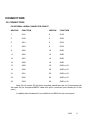
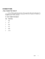
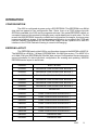
6I25
ANYTHING I/O
MANUAL
Version 1.4
This page intentionally not blank
Table of Contents
GENERAL . . . . . . . . . . . . . . . . . . . . . . . . . . . . . . . . . . . . . . . . . . . . . . . . . . . . . . . . . . 1
DESCRIPTION . . . . . . . . . . . . . . . . . . . . . . . . . . . . . . . . . . . . . . . . . . . . . . . . . 1
HARDWARE CONFIGURATION . . . . . . . . . . . . . . . . . . . . . . . . . . . . . . . . . . . . . . . . 2
GENERAL . . . . . . . . . . . . . . . . . . . . . . . . . . . . . . . . . . . . . . . . . . . . . . . . . . . .
BREAKOUT POWER OPTION . . . . . . . . . . . . . . . . . . . . . . . . . . . . . . . . . . . . .
5V I/O TOLERANCE . . . . . . . . . . . . . . . . . . . . . . . . . . . . . . . . . . . . . . . . . . . .
PRECONFIG PULL-UP ENABLE . . . . . . . . . . . . . . . . . . . . . . . . . . . . . . . . . . .
PCICLOCK SELECTION . . . . . . . . . . . . . . . . . . . . . . . . . . . . . . . . . . . . . . . . .
BRIDGE EEPROM ENABLE . . . . . . . . . . . . . . . . . . . . . . . . . . . . . . . . . . . . . .
2
2
2
3
3
3
CONNECTORS . . . . . . . . . . . . . . . . . . . . . . . . . . . . . . . . . . . . . . . . . . . . . . . . . . . . . . 4
CONNECTOR LOCATIONS AND DEFAULT JUMPER POSITIONS . . . . . . . . 4
6I25 I/O CONNECTOR PIN-OUT . . . . . . . . . . . . . . . . . . . . . . . . . . . . . . . . . . . 5
JTAG CONNECTOR PIN-OUT . . . . . . . . . . . . . . . . . . . . . . . . . . . . . . . . . . . . . 7
OPERATION . . . . . . . . . . . . . . . . . . . . . . . . . . . . . . . . . . . . . . . . . . . . . . . . . . . . . . . . 8
5I25 COMPATIBILITY . . . . . . . . . . . . . . . . . . . . . . . . . . . . . . . . . . . . . . . . . . . 8
FPGA . . . . . . . . . . . . . . . . . . . . . . . . . . . . . . . . . . . . . . . . . . . . . . . . . . . . . . . . 8
FPGA PINOUT . . . . . . . . . . . . . . . . . . . . . . . . . . . . . . . . . . . . . . . . . . . . . . . . . 8
PCIE ACCESS . . . . . . . . . . . . . . . . . . . . . . . . . . . . . . . . . . . . . . . . . . . . . . . . . 8
CONFIGURATION . . . . . . . . . . . . . . . . . . . . . . . . . . . . . . . . . . . . . . . . . . . . . . 9
EEPROM LAYOUT . . . . . . . . . . . . . . . . . . . . . . . . . . . . . . . . . . . . . . . . . . . . . . 9
BIT FILE FORMAT . . . . . . . . . . . . . . . . . . . . . . . . . . . . . . . . . . . . . . . . . . . . . 12
MFLASH . . . . . . . . . . . . . . . . . . . . . . . . . . . . . . . . . . . . . . . . . . . . . . . . . . . . . 12
MESAFLASH . . . . . . . . . . . . . . . . . . . . . . . . . . . . . . . . . . . . . . . . . . . . . . . . . 12
SPI INTERFACE DESCRIPTION . . . . . . . . . . . . . . . . . . . . . . . . . . . . . . . . . . 13
FREE EEPROM SPACE . . . . . . . . . . . . . . . . . . . . . . . . . . . . . . . . . . . . . . . . 14
FALLBACK INDICATION . . . . . . . . . . . . . . . . . . . . . . . . . . . . . . . . . . . . . . . . 14
FAILURE TO CONFIGURE . . . . . . . . . . . . . . . . . . . . . . . . . . . . . . . . . . . . . . 14
CLOCK SIGNALS . . . . . . . . . . . . . . . . . . . . . . . . . . . . . . . . . . . . . . . . . . . . . . 14
LEDS . . . . . . . . . . . . . . . . . . . . . . . . . . . . . . . . . . . . . . . . . . . . . . . . . . . . . . . 15
PULLUP RESISTORS . . . . . . . . . . . . . . . . . . . . . . . . . . . . . . . . . . . . . . . . . . 15
I/O LEVELS . . . . . . . . . . . . . . . . . . . . . . . . . . . . . . . . . . . . . . . . . . . . . . . . . . 15
STARTUP I/O VOLTAGE . . . . . . . . . . . . . . . . . . . . . . . . . . . . . . . . . . . . . . . . 15
INTERFACE CABLES . . . . . . . . . . . . . . . . . . . . . . . . . . . . . . . . . . . . . . . . . . 16
BREAKOUT POWER OPTION . . . . . . . . . . . . . . . . . . . . . . . . . . . . . . . . . . . . 16
PLUG AND GO KITS . . . . . . . . . . . . . . . . . . . . . . . . . . . . . . . . . . . . . . . . . . . 16
iii
Table of Contents
SUPPLIED CONFIGURATIONS . . . . . . . . . . . . . . . . . . . . . . . . . . . . . . . . . . . . . . . . 17
HOSTMOT2 . . . . . . . . . . . . . . . . . . . . . . . . . . . . . . . . . . . . . . . . . . . . . . . . . .
7I76X2 . . . . . . . . . . . . . . . . . . . . . . . . . . . . . . . . . . . . . . . . . . . . . . . . . . . . . .
7I76_7I74 . . . . . . . . . . . . . . . . . . . . . . . . . . . . . . . . . . . . . . . . . . . . . . . . . . . .
G540X2 . . . . . . . . . . . . . . . . . . . . . . . . . . . . . . . . . . . . . . . . . . . . . . . . . . . . .
7I77X2 . . . . . . . . . . . . . . . . . . . . . . . . . . . . . . . . . . . . . . . . . . . . . . . . . . . . . .
7I77_7I76 . . . . . . . . . . . . . . . . . . . . . . . . . . . . . . . . . . . . . . . . . . . . . . . . . . . .
7I77_7I74 . . . . . . . . . . . . . . . . . . . . . . . . . . . . . . . . . . . . . . . . . . . . . . . . . . . .
7I74X2 . . . . . . . . . . . . . . . . . . . . . . . . . . . . . . . . . . . . . . . . . . . . . . . . . . . . . .
7I78X2 . . . . . . . . . . . . . . . . . . . . . . . . . . . . . . . . . . . . . . . . . . . . . . . . . . . . . .
PROB_RFX2 . . . . . . . . . . . . . . . . . . . . . . . . . . . . . . . . . . . . . . . . . . . . . . . . .
PIN FILES . . . . . . . . . . . . . . . . . . . . . . . . . . . . . . . . . . . . . . . . . . . . . . . . . . .
17
17
17
17
17
17
18
18
18
18
18
REFERENCE INFORMATION . . . . . . . . . . . . . . . . . . . . . . . . . . . . . . . . . . . . . . . . . 19
SPECIFICATIONS . . . . . . . . . . . . . . . . . . . . . . . . . . . . . . . . . . . . . . . . . . . . . 19
iv
GENERAL
DESCRIPTION
The MESA 6I25 SuperPort is a low cost, general purpose programmable I/O card
for the PCIE bus. The 6I25 is a low profile one lane PCIE card and is available with standard
or low profile brackets. The 6I25 uses standard parallel port pinouts and connectors for
compatibility with most parallel port interfaced motion control / CNC breakout cards, allowing
a motion control performance boost while retaining a reliable real time PCI interface.
The 6I25 provides 34 I/O bits (17 per connector). All I/O bits have bus switches that
provide 5V tolerance and also have the benefit of disconnecting all I/O pins when the host
CPU is off, preventing damage to the 6I25 if power is supplied to I/O pins when the host is
powered down. All I/O pins have pull-up resistors, so have a defined state at power up.
Unlike the parallel port that the 6I25 replaces, each I/O bit has individually programmable
direction and function.
A power source option allows the 6I25 to supply 5V power to breakout boards if
desired. This 5V power is protected by a per connector PTC.
Configurations are provided for hardware step generation (to MHz rates), encoder
counting, PWM, digital I/O, analog I/O, and Smart Serial remote I/O.Configurations are
available that are compatible with common breakout cards and multi axis step drives like
the Probotix-RF and the Gecko G540.
There are currently six 6I25 compatible breakout cards available from Mesa, the 7I74
through 7I85.
6I25
1
HARDWARE CONFIGURATION
GENERAL
Hardware setup jumper positions assume that the 6I25 card is oriented in an upright
position, that is, with the PCIE connector towards the person doing the configuration.
BREAKOUT POWER OPTION
The 6I25 has the option to supply 5V power from the host computer to the breakout
board. This option is used by all Mesa breakout boards to simplify wiring. The option uses
4 parallel cable signals that are normally used as grounds for supplying 5V to the remote
breakout board (DB25 pins 22,23,24 and 25). These pins are AC bypassed on both the
6I25 and Mesa breakout cards so do not compromise AC signal integrity.
The 5V power option is individually selectable for the two I/O connectors. The
breakout 5V power is protected by per connector PTC devices so will not cause damage
to the 6I25 or system if accidentally shorted. This option should only be enabled for Mesa
breakout boards or boards specifically wired to accept 5V power on DB25 pins 22 through
25. When the option is disabled DB25 pins 22 through 25 are grounded
W1 (P2 POWER ) W2 (P3 POWER)
UP
UP
BREAKOUT POWER ENABLED
DOWN,
DOWN
BREAKOUT POWER DISABLED (DEFAULT)
5V I/O TOLERANCE
The FPGA used on the 6I25 has a 4V absolute maximum input voltage
specification. To allow interfacing with 5V inputs, the 6I25 has bus switches on all I/O pins.
The bus switches work by turning off when the input voltage exceeds a preset threshold.
The 5V I/O tolerance option is the default and should normally be left enabled.
For high speed applications where only 3.3V maximum signals are present and
overshoot clamping is desired, the 5V I/O tolerance option can be disabled. W3 controls
the 5V I/O tolerance option. When W3 is on the default UP position, 5V tolerance mode
is enabled. When W3 is in the DOWN position, 5V tolerance mode is disabled. Note that
W3 controls 5V tolerance on both P2 and P3 I/O connectors.
W3 also selects the pull-up resistor voltage, When 5V I/O tolerance mode is
selected, the I/O pull-up resistors are powered from 5V. When 5V I/O tolerance mode is
disabled, the I/O pull-up resistors are powered with 3.3V.
6I25
2
HARDWARE CONFIGURATION
PRECONFIG PULLUP ENABLE
The Xilinx FPGA on the 6I25 has the option of having weak pull-ups on all I/O pins
at power-up or reset. The default is to enable the pull-ups To enable the built-in pull-ups,
(the default condition) jumper W4 should be placed in the UP position. To disable the
internal pull-ups, W4 should be in the DOWN position.
PCI BUS CLOCK SELECTION
The 6I25 uses a PCIE to PCI bridge chip to interface its FPGA to the PCIE bus.
This bridge chip has selectable PCI bus speeds. Jumpers W8 and W7 select the local PCI
bus clock.
W7
W8
PCI CLOCK
DOWN
DOWN
25 MHz
DOWN
UP
33 MHz
UP
DOWN
50 MHz
UP
UP
66 MHz
NOTE
DEFAULT 5I25 COMPATIBLE
6I25 COMPATIBLE
Note that 33MHz must be selected to be able to use 5I25 bitfiles, and 66 MHz
must be selected in order use 6I25 bitfiles.
BRIDGE EEPROM ENABLE
The 6I25's PCIE bridge has a serial EEPROM to allow storage of bridge setup
options. Since its possible to disable the card with incorrect EEPROM setup options, a
jumper is provided to disable the EEPROM, and thereby load default parameters in case
the EEPROM is corrupted/programmed incorrectly. Jumper W5 determines if the bridge
loads its setup options from the EEPROM or uses default options. When W5 is in the UP
position (default) the bridge chip will load its option from the EEPROM. When W5 is in the
DOWN position, the bridge will not read the EEPROM and instead use its internal defaults.
6I25
3
CONNECTORS
CONNECTOR LOCATIONS AND DEFAULT JUMPER POSITIONS
6I25
4
CONNECTORS
I/O CONNECTORS
The 6I25 has 2 I/O connectors, the primary DB25F connector P3 and the secondary
26 pin header connector P2, please see the 6I25IO.PIN file on the 6I25 distribution disk.
6I25 IO connector pinouts are as follows:
P3 BACK PANEL DB25F CONNECTOR PINOUT
DB25 PIN
FUNCTION
DB25 PIN
FUNCTION
1
IO0
14
IO1
2
IO2
15
IO3
3
IO4
16
IO5
4
IO6
17
IO7
5
IO8
18
GND
6
IO9
19
GND
7
IO10
20
GND
8
IO11
21
GND
9
IO12
22
GND or 5V
10
IO13
23
GND or 5V
11
IO14
24
GND or 5V
12
IO15
25
GND or 5V
13
IO16
6I25
5
CONNECTORS
I/O CONNECTORS
P2 INTERNAL HDR26 CONNECTOR PINOUT
HDR PIN
FUNCTION
HDR PIN
FUNCTION
1
IO17
2
IO18
3
IO19
4
IO20
5
IO21
6
IO22
7
IO23
8
IO24
9
IO25
10
GND
11
IO26
12
GND
13
IO27
14
GND
15
IO28
16
GND
17
IO29
18
GND or 5V
19
IO30
20
GND or 5V
21
IO31
22
GND or 5V
23
IO32
24
GND or 5V
25
IO33
26
GND or 5V
Note: 26 pin header P2 will match standard parallel port pin-out if terminated with
flat cable 26 pin receptacle/DB25F cable with pin1s connected (and header pin 26 left
open)
A cable/bracket hardware kit is available from MESA for the second port.
6I25
6
CONNECTORS
JTAG CONNECTOR PINOUT
P1 is a JTAG programming connector. This is normally used only for debugging .For
debugging, the card can be powered in a standard PCIE slot or if desired, 3.3V power can
be applied via the JTAG connector.
P1 JTAG CONNECTOR PINOUT
PIN
FUNCTION
1
TMS
2
TDI
3
TDO
4
TCK
5
GND
6
+3.3V
6I25
7
OPERATION
5I25 COMPATIBILITY
The 6I25 can be completely software compatible with the 5I25 if 5I25 bitfiles are
loaded in the 6I25's EEPROM, and its PCI clock is set for 33 MHz. This is the current
default setup of 6I25 cards. Configured this way, the 6I25 will report itself as a 5I25 and
will be completely compatible with 5I25 software. These is a small speed advantage and
some additional 6I25 features available if the card is runs as a native 6I25. To do this, a
6I25 bitfile must be loaded in the 6I25's EEPROM, and the local PCI clock set to 66MHz.
FPGA
The 6I25 use a Xilinx Spartan6 ~400k gate FPGA in a 144 pin QFP package:
XC6SLX9-PQ144.
FPGA PINOUT
The local bus and I/O interface FPGA pinouts are described in the 6i25.ucf file in
the /configs/hostmot2/source directory of the 5i25.zip file.
PCIE ACCESS
The 6I25 normally uses 5I25 or 6I25 specific HostMot2 firmware which currently has
a simple target only PCI core with a single Base Address Register (BAR 0). Card specific
PCI identifiers are as follows:
VENDOR ID
0X2718
DEVICE ID (5I25 mode)
0x5125
DEVICE ID (6I25 mode)
0x6125
SUBSYSTEM VENDOR ID
0x2718
SUBSYSTEM DEVICE ID (5I25 mode)
0x5125
SUBSYSTEM DEVICE ID (6I25 mode)
0x6125
The single base address register (BAR0) maps a 64K Byte region of non-cacheble 32 bit
wide memory.
.
6I25
8
OPERATION
CONFIGURATION
The 6I25 is configured at power up by a SPI EEPROM. This EEPROM is an 8M bit
chip that has space for two configuration files. Since there is a PCIE bridge chip with
GPIO bits available, the 6I25 can be programmed even if the serial EEPROM is blank or
corrupted, however this requires bit-banging every serial data bit and is quite slow. For this
reason the 6I25 EEPROM normally contains two configuration file images, A primary user
image and a fallback image. If the primary user configuration is corrupted, the FPGA will
load the fallback configuration so the EEPROM image can be repaired via a fast SPI
interface in the FPGA instead of having to resort to bit banging.
EEPROM LAYOUT
The EEPROM used on the 6I25 for configuration storage is the M25P80 or M25P16.
The M25P80 is a 8 M bit (1 M byte) EEPROM with 16x 64K byte sectors. The M25P16 is
a 16 Mbit (2 M byte) EEPROM with 32x 64K byte sectors Configuration files are stored on
sector boundaries to allow individual configuration file erasing and updating. M25P80
EEPROM sector layout is as follows:
0x00000
BOOT BLOCK
0x10000
FALLBACK CONFIGURATION BLOCK 0
0x20000
FALLBACK CONFIGURATION BLOCK 1
0x30000
FALLBACK CONFIGURATION BLOCK 2
0x40000
FALLBACK CONFIGURATION BLOCK 3
0x50000
FALLBACK CONFIGURATION BLOCK 4
0x60000
FALLBACK CONFIGURATION BLOCK 5
0x70000
RESERVED
0x80000
USER CONFIGURATION BLOCK 0
0x90000
USER CONFIGURATION BLOCK 1
0xA0000
USER CONFIGURATION BLOCK 2
0xB0000
USER CONFIGURATION BLOCK 3
0xC0000
USER CONFIGURATION BLOCK 4
0xD0000
USER CONFIGURATION BLOCK 5
0xE0000
UNUSED/FREE
0xF0000
UNUSED/FREE
6I25
9
OPERATION
EEPROM LAYOUT
The first half of M25P16 sector layout is as follows:
0x00000
BOOT BLOCK
0x10000
FALLBACK CONFIGURATION BLOCK 0
0x20000
FALLBACK CONFIGURATION BLOCK 1
0x30000
FALLBACK CONFIGURATION BLOCK 2
0x40000
FALLBACK CONFIGURATION BLOCK 3
0x50000
FALLBACK CONFIGURATION BLOCK 4
0x60000
FALLBACK CONFIGURATION BLOCK 5
0x70000
RESERVED
0x80000
UNUSED/FREE
0x90000
UNUSED/FREE
0xA0000
UNUSED/FREE
0xB0000
UNUSED/FREE
0xC0000
UNUSED/FREE
0xD0000
UNUSED/FREE
0xE0000
UNUSED/FREE
0xF0000
UNUSED/FREE
6I25
10
OPERATION
EEPROM LAYOUT
The second half of M25P16 sector layout is as follows:
0x100000
USER CONFIGURATION BLOCK 0
0x110000
USER CONFIGURATION BLOCK 1
0x120000
USER CONFIGURATION BLOCK 2
0x130000
USER CONFIGURATION BLOCK 3
0x140000
USER CONFIGURATION BLOCK 4
0x150000
USER CONFIGURATION BLOCK 5
0x160000
UNUSED/FREE
0x170000
UNUSED/FREE
0x180000
UNUSED/FREE
0x190000
UNUSED/FREE
0x1A0000
UNUSED/FREE
0x1B0000
UNUSED/FREE
0x1C0000
UNUSED/FREE
0x1D0000
UNUSED/FREE
0x1E0000
UNUSED/FREE
0x1F0000
UNUSED/FREE
6I25
11
OPERATION
BITFILE FORMAT
The configuration utilities expects standard FPGA bitfiles without any multiboot
features enabled. If multiboot FPGA files are loaded they will likely cause a configuration
failure. In addition for fallback to work, the -g next_config_register_write:disable, -g
reset_on_error:enable and -g CRC:enable bitgen options must be set.
NMFLASH
The DOS utility program NMFLASH is provided to write configuration files to the
6I25 EEPROM under DOS. NMFLASH depends on a simple SPI interface built into both
the standard user FPGA bitfiles and the fallback bitfile.
NMFLASH FPGAFILE.BIT
Writes a standard bitfile FPGAFILE.BIT to the user area of the EEPROM
NMFLASH FPGAFILE.BIT V
Verifies the user EEPROM configuration against the bit file FPGAFILE.BIT
NMFLASH FALLBACK.BIT FallBack
Writes the fallback EEPROM configuration to the fallback area of the EEPROM. In addition
if the bootblock is not present in block 0 of the EEPROM, it re-writes the bootblock.
MESAFLASH
Linux and Windows utility programs mesaflash and mesaflash.exe are provided to
write configuration files to the 6I25 EEPROM. These files depend on a simple SPI
interface built into both the standard user FPGA bitfiles and the fallback bitfile.
If mesaflash is run with a Bhelp command line it will print usage information.
mesaflash --device 5I25 --write FPGAFILE.BIT
Writes a standard bitfile FPGAFILE.BIT to the user area of the EEPROM.
mesaflash --device 5I25 --verify FPGAFILE.BIT
Verifies the user EEPROM configuration against the bit file FPGAFILE.BIT.
mesaflash --device 5I25 --fallback --write FALLBACK.BIT
Writes a fallback file to the fallback area of the EEPROM.
6I25
12
OPERATION
SPI INTERFACE DESCRIPTION
This is the register level description of the simple SPI interface to the 6I25's
configuration EEPROM. This hardware is built into all Mesa 6I25 configurations. This
information is only needed if you are writing your own programming utility.
DATA REGISTER at offset 0x74 from 6I25 base address
D7
D6
D5
D4
D3
D2
D1
D0
R/W
R/W
R/W
R/W
R/W
R/W
R/W
R/W
CONTROL REGISTER at offset 0x70 from 6I25 base address
X
X
X
X
X
DAV
BUSY
CS
X
X
X
X
X
R/O
R/O
R/W
6I25
13
OPERATION
SPI INTERFACE DESCRIPTION
The SPI interface is very minimal, just enough hardware to avoid slow bit banging
of the SPI data when reading or writing the configuration EEPROM. Operation is as
follows: To transfer SPI data, CS is asserted low and an outgoing command/data byte is
written to the data register. This write to the data register causes the SPI interface to clear
its DAV bit, shift out its outgoing data byte, and shift in its incoming data. This shifting is
done at a fixed PCI Clock/3 rate or about 11 MHz. When the byte data transfer is done,
The DAV bit is set in the control register. Host software can poll this bit to determine when
the transfer is done. When the transfer is done the incoming data from the EEPROM can
be read in the data register, and the next byte sent out.
Note that CS operation is entirely controlled by the host, that is for example with a
5 byte command sequence, the host must assert CS low, transfer 5 bytes with 5 write/read
commands to the data register with per byte DAV bit polling and finally assert CS high
when done.
FREE EEPROM SPACE
Three 64K byte blocks of EEPROM space are free when both user and fallback
configurations are installed. It is suggested that only the last two blocks, 0xE0000 and
0xF0000 in the user area, be used for FPGA application EEPROM storage.
FALLBACK INDICATION
Mesa’s supplied fallback configurations blink the red INIT LED on the top right hand
side of the card if the primary configuration fails and the fallback configuration loaded
successfully. If this happens it means the user configuration is corrupted or not a proper
configuration for the 6I25s FPGA. This can be fixed by running the configuration utility and
re-writing the user configuration.
FAILURE TO CONFIGURE
The 6I25 should configure its FPGA within a fraction of a second of power
application. If the FPGA card fails to configure, both red LEDs on the right hand side of
the card will remain illuminated after power up. If this happens the 6I25s EEPROM must
be re-programmed via the slow GPIO bitbanged method with SMFLASH.
CLOCK SIGNALS
The 6I25 has two FPGA clock signals. One is the PCI clock and the other is a 50
MHz crystal oscillator on the 6I25 card. Both clocks a can be multiplied and divided by the
FPGAs clock generator block to generate a wide range of internal clock signals. Note tha
the PCI clock rate is selectable via W7 and W8.
6I25
14
OPERATION
LEDS
The 6I25 has 2 FPGA driven user LEDs (User 0 and User 1 = Green), and 2 status
LEDs (red). The user LEDs can be used for any purpose, and can be helpful as a simple
debugging feature. A low output signal from the FPGA lights the LED. See the 6I25IO.PIN
file for FPGA pin locations of the LED signals. The status LEDs reflect the state of the
FPGA’s DONE, and /INIT pins. The /DONE LED lights until the FPGA is configured at
power-up. The /INIT LED lights when the power on reset is asserted, when there has been
a CRC error during configuration. When using Mesas configurations, the /INIIT LED blinks
when the fallback configuration has been loaded.
PULLUP RESISTORS
All I/O pins are provided with pull-up resistors to allow connection to open drain,
open collector, or OPTO devices. These resistors have a value of 3.3K so have a
maximum pull-up current of 1.5 mA (5V pull-up) or 1 mA (3.3V pull-up).
IO LEVELS
The Xilinx FPGAs used on the 6I25 have programmable I/O levels for interfacing
with different logic families. The 6I25 does not support use of the I/O standards that require
input reference voltages. All standard Mesa configurations use LVTTL levels.
Note that even though the 6I25 can tolerate 5V signal inputs, its outputs will not
swing to 5V. The outputs are push pull CMOS that will drive to the output supply rail of
3.3V. This is sufficient for TTL compatibility but may cause problems with some types of
loads. For example when driving an LED that has its anode connected to 5V, in such
devices as OPTO isolators and I/O module rack SSRs, the 3.3V high level may not
completely turn the LED off. To avoid this problem, either drive loads that are ground
referred, Use 3.3V as the VCC for VCC referred loads, or use open drain mode.
STARTUP I/O VOLTAGE
After power-up or system reset and before the the FPGA is configured, the pull-up
resistors will pull all I/O signals to a high level. If the FPGA is used for motion control or
controlling devices that could present a hazard when enabled, external circuitry should be
designed so that this initial state results in a safe condition.
6I25
15
OPERATION
INTERFACE CABLES
Mesa daughtercards use a male to male DB25 cable to interface to the 6I25. For
noise immunity and signal fidelity it is suggested that only IEEE-1284 rated cables be
used. IEEE-1284 rated cables have a twisted pair shield wire for each signal wire and an
overall shield terminated in the metal connector shell. This results in much better
performance than flat or NON-IEEE-1284 parallel port cables For short connections of less
than 3 feet, flat cables can be used. No other type of cable should be used.
Mesa can supply IEEE-1284 cables tested with the 6I25 / daughtercard combination
in 6 and 10 foot lengths.
BREAKOUT POWER OPTION
When used with Mesa breakout/daughter cards, the 6I25 can supply up to 1A of 5V
power to each of the daughter cards. This option is disabled by default to avoid possible
damage to standard breakout boards, so must be specifically enabled for Mesa
daughtercards. If you use this option you must verify that the interface cable does not tie
the eight parallel port ground wires together as some cheap printer cables do. Mesa
supplied IEEE-1284 cables are the best option for Mesa daughter cards and are
guaranteed to work with the power option. Flat cable will work as well but have poorer
noise immunity and signal fidelity.
PLUG AND GO KITS
Motion control kits with pre-programmed 6I25, interface cable, and daughtercard(s)
are available to simplify system integration.
6I25
16
SUPPLIED CONFIGURATIONS
HOSTMOT2
All supplied configurations are part of the HostMot2 motion control firmware set. All
HostMot2 firmware is open source and easily extendible to support new interfaces or
different sets of interfaces embedded in one configuration. For detailed register level
information on Hostmot2 firmware modules, see the regmap file in the hostmot2 source
code directory.
7I76X2
7I76X2 is a configuration intended to work with the 7I76 five axis step/dir
daughtercard. It will support two 7I76 daughtercards, one on each of the 6I25s I/O
connectors. The configuration includes ten hardware step generators, two encoder inputs
and four Smart Serial interfaces, a watchdog timer and GPIO.
7I76_7I74
7I76_7I74 is a configuration for one 7I76 five axis step/dir daughtercards on P3 and
one 7I74 eight channel RS-422 interface on P2. The 7I74 is configured with eight Smart
Serial channels.
G540X2
G540X2 is a configuration intended to work with two Gecko G540 four axis step
motor drives. It includes eight hardware step generators, two PWM generators, four GPIO
outputs, eight GPIO inputs, two charge pump drivers and a watchdog timer.
7I77X2
7I77X2 is a configuration intended to work with the 7I77 six axis analog servo
daughtercard. It will support two 7I77 daughtercards. It includes twelve encoder inputs, six
smart serial interfaces (four used locally on the 7I77s and two fed through for additional
remotes), a watchdog timer and GPIO.
7I77_7I76
7I77_7I76 is a configuration intended to work with a 7I77 six axis analog servo
daughtercard on P3 and a 7I76 daughtercard on P2.
6I25
17
SUPPLIED CONFIGURATIONS
7I77_7I74
7I74_7I77 is a configuration intended to work with one 7I77 six axis analog servo
daughtercard on P3 and one 7I74 eight channel RS-422 interface daughtercard on P2.
Including It includes 12 encoder inputs, 11 smart serial interfaces (two used on the 7I77
for 48 bit isolated field I/O and analog out) , a watchdog timer and GPIO.
7I74X2
7I74X2 is a configuration intended to work with two 7I74 RS-422 daughter cards
It include sixteen smart serial interfaces allowing real time control of up to 768 digital I/O
points, a watchdog timer and GPIO.
7I78X2
7I78X2 is a configuration intended to work with the 7I78 four axis step/dir
daughtercard. It will support two 7I78 daughtercards, one on each of the 6I25s I/O
connectors. The configuration includes eight hardware step generators, two PWM
generators, two encoder inputs and two Smart Serial interfaces, a watchdog timer and
GPIO
PROB_RFX2
The PROB_RFX2 configuration is a step/dir configuration intended to work with
most common parallel port breakouts. Two breakouts are supported, one on each of the
6I25s I/O connectors. The configuration includes eight hardware step generators, two
encoders with index, two PWM generators , a watchdog timer and GPIO.
PIN FILES
Each of the configurations has an associated file with file name extension .pin that
describes the FPGA functions included in the configuration and the I/O pinout. These are
plain text files that can be printed or viewed with any text editor.
6I25
18
REFERENCE
SPECIFICATIONS
POWER
MIN
MAX
NOTES:
3.3V POWER SUPPLY
3.0V
3.6V
PCI supplied 3.3V
12V POWER SUPPLY
8V
18V
For local 5V supply
3.3V POWER CONSUMPTION:
C
400 mA
Depends on FPGA
Configuration
MAX 5V CURRENT TO I/O CONNS
C
1000 mA
Each (PTC Limit)
TOTAL LOCAL 5V CURRENT
C
1500 mA
Total for both I/O
connectors
TEMPERATURE RANGE -C version
0 oC
+70 oC
TEMPERATURE RANGE -I version
-40 oC
+85 oC
6I25
19