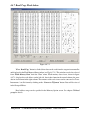
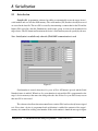
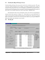
1
GangPro430
USB-MSP430 Gang Flash Programmer
User’s Manual
Software version 3.9-5
PM015A01 Rev.8
February-21-2008
Elprotronic Inc.
16 Crossroads Drive
Richmond Hill,
Ontario, L4E-5C9
CANADA
Web site:
E-mail:
Fax:
Voice:
www.elprotronic.com
[email protected]
905-780-2414
905-780-5789
Copyright © Elprotronic Inc. All rights reserved.
Disclaimer:
No part of this document may be reproduced without the prior written consent of Elprotronic Inc.
The information in this document is subject to change without notice and does not represent a
commitment on any part of Elprotronic Inc. While the information contained herein is assumed to
be accurate, Elprotronic Inc. assumes no responsibility for any errors or omissions.
In no event shall Elprotronic Inc, its employees or authors of this document be liable for special,
direct, indirect, or consequential damage, losses, costs, charges, claims, demands, claims for lost
profits, fees, or expenses of any nature or kind.
The software described in this document is furnished under a licence and may only be used or copied
in accordance with the terms of such a licence.
Disclaimer of warranties: You agree that Elprotronic Inc. has made no express warranties to You
regarding the software, hardware, firmware and related documentation. The software, hardware,
firmware and related documentation being provided to You “AS IS” without warranty or support
of any kind. Elprotronic Inc. disclaims all warranties with regard to the software, express or implied,
including, without limitation, any implied warranties of fitness for a particular purpose,
merchantability, merchantable quality or noninfringement of third-party rights.
Limit of liability: In no event will Elprotronic Inc. be liable to you for any loss of use, interruption
of business, or any direct, indirect, special incidental or consequential damages of any kind
(including lost profits) regardless of the form of action whether in contract, tort (including
negligence), strict product liability or otherwise, even if Elprotronic Inc. has been advised of the
possibility of such damages.
2
END USER LICENSE AGREEMENT
PLEASE READ THIS DOCUMENT CAREFULLY BEFORE USING THE SOFTWARE AND
THE ASSOCIATED HARDWARE. ELPROTRONIC INC. AND/OR ITS SUBSIDIARIES
(“ELPROTRONIC”) IS WILLING TO LICENSE THE SOFTWARE TO YOU AS AN
INDIVIDUAL, THE COMPANY, OR LEGAL ENTITY THAT WILL BE USING THE
SOFTWARE (REFERENCED BELOW AS “YOU” OR “YOUR”) ONLY ON THE CONDITION
THAT YOU AGREE TO ALL TERMS OF THIS LICENSE AGREEMENT. THIS IS A LEGAL
AND ENFORCABLE CONTRACT BETWEEN YOU AND ELPROTRONIC. BY OPENING THIS
PACKAGE, BREAKING THE SEAL, CLICKING “I AGREE” BUTTON OR OTHERWISE
INDICATING ASSENT ELECTRONICALLY, OR LOADING THE SOFTWARE YOU AGREE
TO THE TERMS AND CONDITIONS OF THIS AGREEMENT. IF YOU DO NOT AGREE TO
THESE TERMS AND CONDITIONS, CLICK ON THE “I DO NOT AGREE” BUTTON OR
OTHERWISE INDICATE REFUSAL, MAKE NO FURTHER USE OF THE FULL PRODUCT
AND RETURN IT WITH THE PROOF OF PURCHASE TO THE DEALER FROM WHOM IT
WAS ACQUIRED WITHIN THIRTY (30) DAYS OF PURCHASE AND YOUR MONEY WILL
BE REFUNDED.
1. License.
The software, firmware and related documentation (collectively the “Product”) is the property of
Elprotronic or its licensors and is protected by copyright law. While Elprotronic continues to own
the Product, You will have certain rights to use the Product after Your acceptance of this license.
This license governs any releases, revisions, or enhancements to the Product that Elprotronic may
furnish to You. Your rights and obligations with respect to the use of this Product are as follows:
YOU MAY:
A.
use this Product on many computers;
B.
make one copy of the software for archival purposes, or copy the software onto the hard disk
of Your computer and retain the original for archival purposes;
C.
use the software on a network
YOU MAY NOT:
A.
sublicense, reverse engineer, decompile, disassemble, modify, translate, make any attempt
to discover the Source Code of the Product; or create derivative works from the Product;
B.
redistribute, in whole or in part, any part of the software component of this Product;
3
C.
use this software with a programming adapter (hardware) that is not a product of
Elprotronic Inc.
2. Copyright
All rights, title, and copyrights in and to the Product and any copies of the Product are owned by
Elprotronic. The Product is protected by copyright laws and international treaty provisions.
Therefore, you must treat the Product like any other copyrighted material.
3. Limitation of liability.
In no event shall Elprotronic be liable to you for any loss of use, interruption of business, or any
direct, indirect, special, incidental or consequential damages of any kind (including lost profits)
regardless of the form of action whether in contract, tort (including negligence), strict product
liability or otherwise, even if Elprotronic has been advised of the possibility of such damages.
4. DISCLAIMER OF WARRANTIES.
You agree that Elprotronic has made no express warranties to You regarding the software, hardware,
firmware and related documentation. The software, hardware, firmware and related documentation
being provided to You “AS IS” without warranty or support of any kind. Elprotronic disclaims all
warranties with regard to the software and hardware, express or implied, including, without
limitation, any implied warranties of fitness for a particular purpose, merchantability, merchantable
quality or noninfringement of third-party rights.
4
This device complies with Part 15 of the FCC Rules.
Operation is subject to the following two conditions:
(1) this device may not cause harmful interference and
(2) this device must accept any interference received,
including interference that may cause undesired
operation.
NOTE: This equipment has been tested and found to comply with the limits for a Class B digital devices,
pursuant to Part 15 of the FCC Rules. These limits are designed to provide reasonable protection against harmful
interference in a residential installation. This equipment generates, uses, and can radiate radio frequency energy
and, if not installed and used in accordance with the instruction manual, may cause harmful interference to
radio communications. However, there is no guarantee that interference will not occur in a particular
installation. If this equipment does cause harmful interference to radio or television reception, which can be
determined by turning the equipment off and on, the user is encouraged to try to correct the interference by one
of more of the following measures:
*
Reorient or relocate the receiving antenna
*
Increase the separation between the equipment and receiver
*
Connect the equipment into an outlet on a circuit different from that to which the receiver is connected
*
Consult the dealer or an experienced radio/TV technician for help.
Warning: Changes or modifications not expressly approved by Elprotronic Inc. could void the user’s authority
to operate the equipment.
This Class B digital apparatus meets all requirements of the Canadian
Interference-Causing Equipment Regulations.
Cet appereil numerique de la classe B respecte toutes les exigences du
Reglement sur le material brouilleur du Canada.
5
Table of Contents
1. Introduction . . . . . . . . . . . . . . . . . . . . . . . . . . . . . . . . . . . . . . . . . . . . . . . . . . . . . . . . . . . . . 8
2. Features . . . . . . . . . . . . . . . . . . . . . . . . . . . . . . . . . . . . . . . . . . . . . . . . . . . . . . . . . . . . . . .
2.1
Customized features . . . . . . . . . . . . . . . . . . . . . . . . . . . . . . . . . . . . . . . . . . .
2.1.1 Script file . . . . . . . . . . . . . . . . . . . . . . . . . . . . . . . . . . . . . . . . . . . . . .
2.1.2 DLLs . . . . . . . . . . . . . . . . . . . . . . . . . . . . . . . . . . . . . . . . . . . . . . . . .
10
11
11
11
3. Getting Started . . . . . . . . . . . . . . . . . . . . . . . . . . . . . . . . . . . . . . . . . . . . . . . . . . . . . . . . . .
3.1
Software Installation . . . . . . . . . . . . . . . . . . . . . . . . . . . . . . . . . . . . . . . . . . .
3.2
Hardware Setup . . . . . . . . . . . . . . . . . . . . . . . . . . . . . . . . . . . . . . . . . . . . . . .
3.3
Starting up “GangPro430" Flash Programmer . . . . . . . . . . . . . . . . . . . . . . .
3.4
X-Pro430 Selector . . . . . . . . . . . . . . . . . . . . . . . . . . . . . . . . . . . . . . . . . . . . .
12
12
13
14
14
4. Programming Dialogue Screen . . . . . . . . . . . . . . . . . . . . . . . . . . . . . . . . . . . . . . . . . . . . .
4.1
Microcontroller Type . . . . . . . . . . . . . . . . . . . . . . . . . . . . . . . . . . . . . . . . . . .
4.2
Code File Management . . . . . . . . . . . . . . . . . . . . . . . . . . . . . . . . . . . . . . . . .
4.3
Blow Security Fuse and Open Password File . . . . . . . . . . . . . . . . . . . . . . . .
4.4
Power Device from Adapter . . . . . . . . . . . . . . . . . . . . . . . . . . . . . . . . . . . . .
4.5
Target Device selector and action result . . . . . . . . . . . . . . . . . . . . . . . . . . . .
4.6
Device Action box . . . . . . . . . . . . . . . . . . . . . . . . . . . . . . . . . . . . . . . . . . . . .
4.6.1 Auto Program button . . . . . . . . . . . . . . . . . . . . . . . . . . . . . . . . . . . . .
4.6.2 Verify Security Fuse . . . . . . . . . . . . . . . . . . . . . . . . . . . . . . . . . . . . . .
4.6.3 Erase Flash button . . . . . . . . . . . . . . . . . . . . . . . . . . . . . . . . . . . . . . .
4.6.4 Blank Check button . . . . . . . . . . . . . . . . . . . . . . . . . . . . . . . . . . . . . .
4.6.5 Write Flash button . . . . . . . . . . . . . . . . . . . . . . . . . . . . . . . . . . . . . . .
4.6.6 Verify Flash button . . . . . . . . . . . . . . . . . . . . . . . . . . . . . . . . . . . . . .
4.6.7 Read/ Copy Flash button . . . . . . . . . . . . . . . . . . . . . . . . . . . . . . . . . .
4.7
Next button . . . . . . . . . . . . . . . . . . . . . . . . . . . . . . . . . . . . . . . . . . . . . . . . . .
16
17
19
23
24
26
27
28
28
29
29
30
30
31
33
5. Data viewers . . . . . . . . . . . . . . . . . . . . . . . . . . . . . . . . . . . . . . . . . . . . . . . . . . . . . . . . . . . 34
6. Memory Option Dialogue Screen . . . . . . . . . . . . . . . . . . . . . . . . . . . . . . . . . . . . . . . . . . . 37
6.1
Memory Erase/Write/Verify Group . . . . . . . . . . . . . . . . . . . . . . . . . . . . . . . . 37
GangPro430 - USB-MSP430 Flash Gang Programmer
PM015A01 Rev.8
6
6.2
6.3
Read Group . . . . . . . . . . . . . . . . . . . . . . . . . . . . . . . . . . . . . . . . . . . . . . . . . . 40
Verification Group . . . . . . . . . . . . . . . . . . . . . . . . . . . . . . . . . . . . . . . . . . . . . 40
7. Adapter Options . . . . . . . . . . . . . . . . . . . . . . . . . . . . . . . . . . . . . . . . . . . . . . . . . . . . . . . . .
7.1
JTAG/SBW/BSL Communication Dialogue Box . . . . . . . . . . . . . . . . . . . . .
7.1.1 Communication Interface . . . . . . . . . . . . . . . . . . . . . . . . . . . . . . . . . .
7.1.2 JTAG Communication Speed . . . . . . . . . . . . . . . . . . . . . . . . . . . . . .
7.1.3 BSL Communication Speed . . . . . . . . . . . . . . . . . . . . . . . . . . . . . . . .
7.1.4 Spy-Bi-Wire Communication Speed . . . . . . . . . . . . . . . . . . . . . . . . .
7.2
Reset Dialogue Box . . . . . . . . . . . . . . . . . . . . . . . . . . . . . . . . . . . . . . . . . . . .
7.2.1 Reset pulse duration . . . . . . . . . . . . . . . . . . . . . . . . . . . . . . . . . . . . . .
7.2.2 Final Target Device action . . . . . . . . . . . . . . . . . . . . . . . . . . . . . . . . .
7.3
Options Dialogue Box . . . . . . . . . . . . . . . . . . . . . . . . . . . . . . . . . . . . . . . . . .
42
42
42
43
43
43
44
44
45
46
8. Serialization . . . . . . . . . . . . . . . . . . . . . . . . . . . . . . . . . . . . . . . . . . . . . . . . . . . . . . . . . . . .
8.1
Introduction . . . . . . . . . . . . . . . . . . . . . . . . . . . . . . . . . . . . . . . . . . . . . . . . . .
8.2
Serialization Dialogue Screen . . . . . . . . . . . . . . . . . . . . . . . . . . . . . . . . . . . .
8.2.1 Serial number File . . . . . . . . . . . . . . . . . . . . . . . . . . . . . . . . . . . . . . .
8.2.2 Serial number formats . . . . . . . . . . . . . . . . . . . . . . . . . . . . . . . . . . . .
8.2.3 Model, Group, Revision . . . . . . . . . . . . . . . . . . . . . . . . . . . . . . . . . . .
8.2.4 Device Serialization box . . . . . . . . . . . . . . . . . . . . . . . . . . . . . . . . . .
8.3
Serialization Report Dialogue Screen . . . . . . . . . . . . . . . . . . . . . . . . . . . . . .
8.4
SN data file . . . . . . . . . . . . . . . . . . . . . . . . . . . . . . . . . . . . . . . . . . . . . . . . . .
47
47
48
49
49
58
58
60
60
10. DCO calibration . . . . . . . . . . . . . . . . . . . . . . . . . . . . . . . . . . . . . . . . . . . . . . . . . . . . . . . 67
11. Load/Save Setup . . . . . . . . . . . . . . . . . . . . . . . . . . . . . . . . . . . . . . . . . . . . . . . . . . . . . . . . 69
11.1 User defined programming sequence - Scrip File . . . . . . . . . . . . . . . . . . . . . 72
12. Target connection . . . . . . . . . . . . . . . . . . . . . . . . . . . . . . . . . . . . . . . . . . . . . . . . . . . . . . 78
Appendix A - specification . . . . . . . . . . . . . . . . . . . . . . . . . . . . . . . . . . . . . . . . . . . . . . . . . . 87
Appendix B - Self Test Program . . . . . . . . . . . . . . . . . . . . . . . . . . . . . . . . . . . . . . . . . . . . . . 89
GangPro430 - USB-MSP430 Flash Gang Programmer
PM015A01 Rev.8
7
1. Introduction
GangPro430 programmer is dedicated to simultaneously program up to six the Texas
Instruments MSP430Fxx family microcontrollers. Using GangPro430 programmer the target
devices can be programmed via JTAG, SBW (Spy-Bi-Wire) or BSL (Boot Strap Loader) Interface.
Each programmer package consist of a microcontroller based adapter (Figure 1-1),
WindowsTM based software and cable to connect the adapter with the computer’s USB port. The
internal adapter software allows to communicate with the programmed device with the high speed.
The effective programming speed is
around 12 kbytes/s simultaneously up to
six target devices that is equivalent to 72
kbytes/s programming speed per one
programmed target device. Due to this
high speed communication,
programming time is very short and
programmer can be used to program
flash devices in the production process.
For example, six microcontrollers with
60 kB Flash, such as MSP430F149, can
Figure 1-1
be programmed in 8 seconds. This time
includes initialization, erasing memory,
blank checking, programming and fast
verification.
The Gang Splitter (Figure 1-2)
(sold separately) allows to connect up
to six target devices to one Gang
Programming Adapter. Communication
via JTAG, Spy-Bi-Wire or BSL is
provided in the same Gang Splitter..
Figure 1-2
To simplify production process the programming software package can assign serials
number, model type, and revision. Each serial number is unique for each programmed device and
is assigned automatically. Several serial number formats are available.
GangPro430 - USB-MSP430 Flash Gang Programmer
PM015A01 Rev.8
8
There are a number of erase/write options also available. This allows to erase/write all flash
memory, or just the specified fragment of memory. This feature is very useful when only part of
programmed data/code should be replaced. For example this feature can be used to download the
serial number, calibration data or personality data without losing existing program code.
GangPro430 - USB-MSP430 Flash Gang Programmer
PM015A01 Rev.8
9
2. Features
GangPro430 programmer is dedicated to simultaneously program up to six the Texas
Instruments MSP430Fxx family microcontrollers via JTAG, SBW or BSL interface. Detailed
information describing features of the JTAG communication port can be found in the Texas
Instruments ( TI ) documentation - SLAA149 -“Programming a Flash-Based MSP430 Using the
JTAG Interface”.
To facilitate high speed communication via the JTAG port, an application software for the
programming adapter has been optimized for the maximum speed. Also a few new procedures have
been implemented, decreasing the flash programming time.
When the BSL Interface is used, then the GangPro430 programmer is using the standard
BSL communication port, available on all MSP430 microcontrollers. Detailed information
describing features of the standard BSL can be found in the Texas Instruments ( TI ) documentation
- SLAA089A -“Features of the MSP430 Bootstrap Loader”.
To facilitate high speed communication a new Fast Bootstrap Loader (Fast BSL) (proprietary
of Elprotronic Inc.) is temporary downloaded to the RAM of each programmed device.
Major features of the GangPro430 programmer are:
*
Support all MSP430Fxx microcontrollers from TI.
*
Programming speed via JTAG interface is approximately 12 kBytes/s simultaneously up to
six target devices that is equivalent to 72 kbytes/s programming speed per one programmed
target device,
*
Programming speed via BSL interface is 9.6 kbits/s ( BSL) and 150 kbits/s (Fast BSL).
*
Our programmers are professionally made and are recommended by Texas Instruments
as the Third Party Tools source.
*
Our programmers are currently the fastest programmers on the market.
*
Blow the JTAG security fuse capability.
*
Full memory or sector memory erase capability.
*
Write Check Sum verification.
*
No code size limitations.
*
Target device can be powered from the programming adapter or from external source.
*
Easy to use WindowsTM based software.
*
Programmer accept TI (*.txt), Motorola (*.s19) and Intel (*.hex) data files for programming.
*
Combine code files capability.
*
Lock setup capability, useful in production.
GangPro430 - USB-MSP430 Flash Gang Programmer
PM015A01 Rev.8
10
*
*
*
Software package can assign and automatically increment serial number, model type and
revision. Serial Number with or without an automatically inserted current date can be stored
in the FLASH memory in HEX, BCD or ASCII format. Log file capability allowing to
review information about the flashed target devices.
DLL software package can control programmer from other programs.
Programmer has been fully tested to comply with the FCC and CE requirements.
Uses USB-1.1 (12Mbits/s) Port to communicate with the Programming Adapter.
2.1
Customized features
*
GangPro430 programmer can be controlled from external software or programming
sequences can be customized. These features are very useful in production environment. Standard
programming software GangPro430 has a lot of options described above, but of course it can not
cover all customer’s requirements.
2.1.1 Script file
To extend programming features programming software supports user defined programming
sequences saved in the script file. That easy method can be created by any user without knowing
programming languages and techniques. Programming sequence up to 1000 lines can be created. All
lines contains sequence of the pressed buttons with extra few condition options. This programming
method is described in chapter 10 on this manual. Script file option is not available in lite software
version.
2.1.2 DLLs
When the customized programming sequence is not covering customer’s requirements, then
an attached to software package DLLs can be used. DLLs allows to fully control programming
adapter from external software written in MS Visual C++, MS Visual Basic, LABView, DOS or
other programming packages like Borland C++ etc. See “GangPro430 FlashProgrammer - Remote
Control Programming User’s Guide” for details.
2.1.3 Self Test Program
Software package contains the Self Test program, that allows to check the adapter, target
device and connection functionality. The Self Test program uses the API-DLL for communication
between Self Test Program and hardware. See Appendix B in this manual for details.
GangPro430 - USB-MSP430 Flash Gang Programmer
PM015A01 Rev.8
11
3. Getting Started
1.
2.
3.
4.
GangPro430 programmer package contains:
One READ ME FIRST document.
One X-Pro430 - USB-MSP430 Flash Programmer CD ROM (Software + Manual).
One GangPro430 Flash Programming Adapter.
One 6 feets length USB-A to USB-B cable.
3.1
Software Installation
The X-Pro430 USB MSP430 Flash Programming Software runs on PC under Windows TM ME,
WinNT, 2000 or XP. Follow instructions below to install the software:
1.
2.
3.
4.
Insert X-Pro430 (the USB MSP430 Flash Programming) Software CD into your CD-ROM
drive.
The X-Pro430 Setup wizard appears automatically. Click Install X-Pro430 Programmer to
begin the installation process.
If the Setup wizard does not start automatically, click the Start button and choose the Run
dialogue box. Type “D:\SETUP.EXE”, where D represents the drive letter of your CD-ROM
drive. Then click the OK button.
Once the installation program starts, on-screen instructions will guide you through the
remainder of the installation. You must accept licence agreement before using software.
Driver Installation
1.
2.
2.
3.
Plug in USB-MSP430-FPA to the PC USB Port, using provided cable extender (USB-A to
USB-B).
==== Windows XP ====
The “New hardware has been found” should be displayed. Follow the wizard instruction
to install the drivers. Drivers are located
in the CD ROM directory
“D:\drivers\W2000,ME,XP”, where “D” represents the drive letter of your CD-ROM drive
or in the application software directory
C:\Program Files\Elprotronic\XPro USB Drivers\W2000,ME,XP
==== Windows - 2000, 98-SE ====
The “New hardware has been found” should be displayed. Follow the wizard instruction
to install the drivers.
Press ‘Next’ when the Device Wizard Driver screen appear.
GangPro430 - USB-MSP430 Flash Gang Programmer
PM015A01 Rev.8
12
4.
5.
6.
7.
Select the following option on the wizard screen:
* select for a suitable driver for my device (recommended)”
and press ‘Next’.
Select the third option - “Specify a location” for a location of the Driver Files.
From the browser select the “D:\drivers\W2000,ME,XP” for Win-2000 or
“D:\drivers\W98” for Win-98SE directory, where D:CD-ROM drive location or in the
application software directory
C:\Program Files\Elprotronic\XPro USB Drivers\W98
and press ‘Next’.
Driver installation process will start.
Driver installation procedures should be done twice. Software will install two USB drivers - the Boot
driver and the Application driver. Reboot computer on the end.
3.2
Hardware Setup
Figure 3.2-1 show connection between PC, GangPro430 adapter, Gang Splitter and target devices.
Figure 3.2-1
1.
2.
Connect the GangPro430 adapter ( USB-MSP430-FPA-GANG) to the PC USB Port, using
provided cable extender (USB-A to USB-B).
Plug in socket connector from the GangPro430 Adapter to the header connector of the Gang
Splitter and from the Gang Splitter connector #1 to #6 to on your device boards. Make sure
that pin 1 on your device board’s header is connected to pin 1 of the socket connector. Pin
1 is marked as a red cable on the ribbon cable.
GangPro430 - USB-MSP430 Flash Gang Programmer
PM015A01 Rev.8
13
3.3
Starting up “GangPro430" Flash Programmer
To start the GangPro430 Flash Programmer click on the GangPro430 Elprotronic icon.
Figure 3.3-1
Once started the software will attempt to access the programming adapter. If no error messages
appear then the software has initialized without a problem and you may begin using it. However, if
the programming adapter is not detected an error message will appear. To correct the problem, make
sure that the connection cable is properly attached and the USB driver is installed.
3.4
X-Pro430 Selector
The X-Pro430 (FlashPro430, ChainPro430 and GangPro430) has Multi-USB feature. Up to 8
Flash Programming Adapters can be connected to one PC. Each adapter can be controlled by one
opened software application. Up to eight application software can be opened at the same time. Each
application software can have independent setup from the other application software setup (code file,
controlled microcontroller type etc.)
When more then one X-Pro430 Adapter is connected to PC then following X-Pro430 Selector
dialogue screen will be displayed on the PC screen (see Figure 3.4-1). Using available buttons the
one desired Flash Programming Adapter should be selected. Make a sure, that selected X-Pro430
is not used by other opened application.
Selected X-Pro430’s serial number will be displayed on the left bottom side of the programming
dialogue screen.
GangPro430 - USB-MSP430 Flash Gang Programmer
PM015A01 Rev.8
14
Figure 3.4-1
GangPro430 - USB-MSP430 Flash Gang Programmer
PM015A01 Rev.8
15
4. Programming Dialogue Screen
The programming dialogue box (see Fig. 4-1.) contains a pull down menu, interface selection
box, blow fuse box, device action buttons, report (status) window, open file buttons, processor
information box, serial number box, power DC status and check sum result boxes.
Figure 4-1. Programming dialogue box screen.
GangPro430 - USB-MSP430 Flash Gang Programmer
PM015A01 Rev.8
16
All device action buttons, power ON/OFF button and the check sum result box have their
own status indicators. Each indicator can assume any of the following conditions:
- blank - idle status.
- yellow - Test in progress. For power on/off - DC voltage is correct.
- green - access enabled.
- red sign - access denied. For power on/off - DC voltage is too low (below 2.6V)
- device action has been finished successfully.
- device action has been finished, but result failed.
- applies to blank check only - Memory is not clean, but the specified memory segment is.
4.1
Microcontroller Type
The microcontroller type can be selected from the pull down
field of the processor type group. The pull down field contains a list of
all microcontrollers in MSP430Fxx family currently available. One
thing to note, the microcontroller type can be selected automatically if
the option ‘Any’ is selected.
When communication between microcontroller and
programming adapter is initialized, the software will detect the target
microcontroller’s automatically. The type of detected microcontroller
is displayed in the field ‘Target:’. This allows the software to warn you
if the connected microcontroller does not match the one specified by the
user.
Note: No warning message will appear when ‘Any’ microcontroller
type is selected.
Texas Instruments has been created number of microcontroller’s
groups and numbers of the microcontroller’s type. Microcontrollers
with the same group has the same ID number saved in the ROM at the
location 0x0FF0. Microcontrollers with the same group ID has a similar
features with a different size of RAM and FLASH.
GangPro430 - USB-MSP430 Flash Gang Programmer
Figure 4.1-1
PM015A01 Rev.8
17
Contents of the ROM at location 0x0FF0 containing ID number can be read using
JTAG/SBW or BSL communication. Particular type of the microcontroller in the same group ID can
be detected when communication via JTAG/SBW is available, but this feature is not available via
BSL interface communication. For programming flash feature knowledge of the type of the
microcontrollers is not required al long as size of FLASH is available.
In the example the four groups of microcontrollers are shown below. Tables contains
following information:
- in [F112] - ID (in HEX format) taken from the ROM at location 0x0FF0,
- F11x(1) - information displayed in the microcontroller type window in programmer dialogue box,
- list of available microcontrollers in particular group with RAM and Flash size specification.
[ F112 ]
F11x(1)
Name
RAM size [bytes]
MSP430F110
MSP430F1101
MSP430F1101A
MSP430F1111A
MSP430F112
MSP430F1121
MSP430F1121A
[ 1132 ]
RAM size [bytes]
MSP430F1122
MSP430F1132
RAM size [bytes]
MSP430F122
MSP430F123
Name
256
256
ROM size [kbytes]
4k
8k
F122..F123
Name
[ F149 ]
1k
1k
1k
2k
4k
4k
4k
F11x2
Name
[ F123 ]
128
128
128
128
256
256
256
ROM size [kbytes]
256
256
ROM size [kbytes]
4k
8k
F13x..F14x
RAM size [bytes]
ROM size [kbytes]
GangPro430 - USB-MSP430 Flash Gang Programmer
PM015A01 Rev.8
18
MSP430F133
MSP430F135
MSP430F147
MSP430F1471
MSP430F148
MSP430F1481
MSP430F149
MSP430F1491
256
512
1024
1024
2048
2048
2048
2048
8k
16 k
32 k
32 k
48 k
48 k
60 k
60 k
When ‘Any’ microcontroller type is selected then only name of the microcontroller’s group
like F13x..F14x is displayed in the Target microcontroller type. Because type of microcontroller
can not be fully detected (especially via BSL Interface) then the max. FLASH from the particular
group is assigned, eg. 60kB for the group F13x..F14x (see table above). If the correct size of the
FLASH is required then the desired microcontroller type should be selected. When communication
with the target device is established and when the selected and the target microcontrollers are from
the same group, then a size of the target device are taken from the selected microcontroller type data
table. In this case the full name of the microcontroller’s is displayed in the Target microcontroller
type field like MSP430F149 instead the group name F13x..F14x only. Otherwise the
microcontroller with the maximum size of FLASH from the detected group is selected (shown in
bold in the tables above) and group name is displayed like F13x..F14x.
4.2
Code File Management
GangPro430 flash programmer provides three options to manage code files. These options
allow the user to open a code file, combine several code files into a single file, and save the
programming data into a code file. The Open Code File button, or the Open Code File from the
FILE pull down menu, prompts for opening the object file that contains the code data, as shown in
Figure 4.2-1. When the file is selected the contents of the object file are downloaded into the PC
memory. If the selected microcontroller does not have enough memory to fit the data contained in
the code file, the warning message in Figure 4.2-2 will be displayed.
GangPro430 - USB-MSP430 Flash Gang Programmer
PM015A01 Rev.8
19
Figure 4.2-1
Figure 4.2-2
When code file is open and read successfully the code file name and full path will be
displayed on the right side of the Open Code File button (see Fig.4-1 Programming dialogue box
screen). Contents of the selected file can be viewed by the selecting of ‘Code File Data’ from the
‘View’ menu (see chapter 5).
The Combine Code Files option allows up to 40 code files to be loaded into the PC memory.
When this option is selected the programmer will create a new data block, which will contain the
combined data of the user selected files. In order to add a code file to the newly created data block,
the user needs to press the ADD Code File button. The programmer will then prompt the user to
GangPro430 - USB-MSP430 Flash Gang Programmer
PM015A01 Rev.8
20
specify the code file to be appended to the newly created memory block, using the window in Figure
4.2-1. Every appended file will be verified, so that the total code size does not exceed the target
microcontroller’s memory space and that there is no overlap with previously selected code segments.
After the addition of each file the window in Figure 4.2-3 will be shown. The window shows the
status of previous append operations.
Figure 4.2-3
The Programmer is also able to append files of any type to the new data block. In order to do this the
user must specify the memory location into which the programmer is to load the file and then press
the Add file contents button. The window in Figure 4.2-1 will appear prompting the user to specify
the file to be added. Once the file is added to the new memory block, the programmer will display
the memory space occupied by the selected file. An example of this is shown in Figure 4.3-3 for the
file number 4.
The Save Code File option saves the data currently contained within the PC code data block
into a code file. When the user selects this option from the File menu, the window in Figure 4.2-4
will appear, prompting for the name of the file to be created.
All of the aforementioned Code File options work with three most popular code file formats.
These formats are the Texas Instruments, the Motorola and the Intel file formats. FlashPro430 will
work with any of these formats and will easily convert one file format to another by using the Open
Code File and Save Code File options.
GangPro430 - USB-MSP430 Flash Gang Programmer
PM015A01 Rev.8
21
Figure 4.2-4
GangPro430 - USB-MSP430 Flash Gang Programmer
PM015A01 Rev.8
22
4.3
Blow Security Fuse and Open Password File
The microcontroller’s memory is protected against unauthorized access. When the
microcontroller is accessed via the JTAG/SBW interface, then the Security Fuse if blown is
protecting access to the microcontroller. Blowing the Security Fuse is not reversible and when done,
then the JTAG/SBW interface becomes unusable.
When JTAG/SBW interface is selected, then ‘Verify Security Fuse’ button allows to
verification, if the fuse is blown or not. Fuse is verified also at the beginning of any device action
command.
To blow the Security Fuse the check mark ‘Enable’ must be selected first (see Figure 4.3-1).
Figure 4.3-1
Because blowing of the Security Fuse is not reversible, the following warning message is displayed
when check mark is selected to be enabled.
Figure 4.3-2
Note: If the option of blowing the Security Fuse is enabled, then if AUTO PROGRAM device action
is selected, the fuse will be blown without warning.
When ‘BLOW FUSE’ button is pressed, then two following warnings are displayed, before fuse will
be blown.
GangPro430 - USB-MSP430 Flash Gang Programmer
PM015A01 Rev.8
23
Figure 4.3-3
Figure 4.3-4
When the button ‘YES’ is pressed twice, the procedure of blowing the security fuse will be initiated.
When Security Fuse is blown, the JTAG/SBW interface becomes inoperable.
4.4
Power Device from Adapter
The programming adapter is powered from the USB Port interface. Target device can be
powered from the programming adapter with voltage range from 2.2V to 3.6V in step 0.2V selected
in the voltage selector located in the ‘Power Device
from Adapter” box.
Target device will be powered from the adapter,
if check box ‘Enable’ in the ‘Power Device from
Adapter’ group (figure 4.4-1) is selected. When the
‘Enable’ checkbox is selected a warning message
shown in figure 4.4-2 will be displayed. If you confirm
this selection by clicking YES, then POWER ON/OFF
button is enabled. By clicking POWER ON/OFF button
Figure 4.4-1
you can turn the power on or off on the target device.
GangPro430 - USB-MSP430 Flash Gang Programmer
PM015A01 Rev.8
24
Current DC voltage on the target device is permanently monitored and displayed in the ‘Device
Voltage’ field in the ‘Power Device from Adapter’ group, even if the target device is powered from
the external DC sources. If DC voltage is higher then 2.7 V, then yellow box will be displayed,
indicating that DC voltage is OK and target device is fully functional under this DC voltage. If DC
level is below 2.7V, but higher then 1V, then access denied sign box will be displayed (red sign with
white line). If DC level is below 1V, then blank sign box will be displayed.
Figure 4.4-2
When the target device is powered from its own power supply or battery then the check box ‘Enable’
should not be selected.
RESET button located on the left side on the POWER ON/OFF button (Figure 4.1) can
generate reset pulse to the target device. Pressing this button the target devices can be reset manually
at any time, starting the target’s device application program from the beginning.
GangPro430 - USB-MSP430 Flash Gang Programmer
PM015A01 Rev.8
25
4.5
Target Device selector and action result
Figure 4.5-1
GangPro430 - USB-MSP430 Flash Gang Programmer
PM015A01 Rev.8
26
4.6
Device Action box
Device Action box contains 9 buttons (see Figure 4.6-1) Each
button allows a specific action to be executed. Software procedures related
to each action allow you to fully execute the desired task, without the need
to follow a specific sequence of actions. Every action starts by powering up
the target device, if Power Device from the Adapter is enabled. When the
DC voltage level becomes higher then 2.7V, the communication with the
target device is initiated via JTAG/SBW Interface. The security fuse is
verified, if access to the microcontroller is available. Once the specified
action is completed successfully the green check marks will appear (see
Figure 4.5-1). Also, the device will return to the state it was in before the
action was executed.
Progress of all actions is displayed in the report window. If the
particular action has been finished successfully, then message ‘done’ or
‘OK’ will appear on the right side of processed procedure (Fig.4.6.2). If
not, a message ‘failed’ will be displayed and selected action will be
terminated. Final status is also displayed in the Status window (see
Fig.4.6-3) as Active (blue), Pass (green), or Fail (red). On the bottom of
Figure 4.6-1
the programmer dialogue screen the progress bar is displayed and the total
run time is shown in the report window.
Run time does not include the time
when user interaction is required.
Figure 4.6-3
Figure 4.6-2
GangPro430 - USB-MSP430 Flash Gang Programmer
PM015A01 Rev.8
27
4.6.1 Auto Program button
Auto Program button is the most frequently used button when programming microcontrollers
in the production process. Auto Program button activates all required procedures to fully program
and verify the flash memory contents. Typically, when flash memory needs to be erased, Auto
Program executes the following procedures:
- reload code file when “Reload Code File” is selected
(useful for debugging when the code file is frequently modified)
- initialization
- read labelling information (Serial Number, Model, Group, Revision) (optional)
- erase flash memory,
- confirm if memory has been erase,
- flash programming and verification,
- labelling information generation,
- flash memory check sum verification,
- retrieve labelling information,
- blowing the security fuse (if enabled).
In the report window you can see a typical report message during the Auto Program
procedure (see Fig. 4.6-2 ).
Status window (see fig. 4.6-3) has a counter that is useful in production process. The total
number of programmed microcontrollers can be entered in the Total edit line. The Balance line
shows the number of microcontrollers that have not been programmed yet. The Balance counter is
initialized to the value entered in the Total edit line and is decremented every time Auto Program
is completed successfully.
Note: Balance counter works only with Auto Program procedure.
4.6.2 Verify Security Fuse
This button allows the security fuse or the password to be verified. This is useful, if you try
to find the correct password from a few available password files, or to check if the security fuse is
blown. This procedure is used for test purposes only.
GangPro430 - USB-MSP430 Flash Gang Programmer
PM015A01 Rev.8
28
4.6.3 Erase Flash button
This button enables the flash memory segments, or mass (all) memory to be erased. If any
option other then ‘Erase All Memory’ is selected in the Memory Options Setup (see chapter 6.1
Memory Erase/Write/Verify Group for details), then the following question message box will be
displayed:
Figure 4.6.3-1
4.6.4 Blank Check button
When Blank Check button is clicked, the program checks if flash memory of the target
microcontroller is blank (all bytes contain the value 0xFF). This test checks if either all memory is
clean, or just the specified memory segment. The first test checks all memory contents. If it fails,
then just the specified memory segment is checked (see setup in Memory Erase/Write Group). The
following conditions can appear at the completion of this operation:
- all memory is blank
- all memory is not blank, but selected part of it is.
- memory is not blank.
GangPro430 - USB-MSP430 Flash Gang Programmer
PM015A01 Rev.8
29
4.6.5 Write Flash button
When write flash button is clicked, then contents from the code file will be written to the
flash memory.
Note: See chapter 5.1 Memory Erase/Write Group for details on how to specify memory segment
for writing.
When the second time target device is programmed, then the following warning message is displayed
Figure 4.6.5-1
4.6.6 Verify Flash button
The Verify Flash function compares the contents of the flash memory with data from the code
file. Verify flash function initiated this way will always use the standard memory verification
method, even if the fast verification method is selected from the memory write verification options
(see chapter 5. Memory Option Dialogue Screen).
Note: During the verification process either all memory or just the selected part of the memory is
verified, depending on settings specified in the Memory Erase/Write Address Range in the
Memory Options setup. See chapter 5.1 Memory Erase/Write Group for details.
GangPro430 - USB-MSP430 Flash Gang Programmer
PM015A01 Rev.8
30
4.6.7 Read/ Copy Flash button
Figure 4.6.7-1
When ‘Read/Copy’ button is clicked, then data can be read from the target microcontroller
and displayed in the Flash Memory Data window (see Fig.4.6.7-1). This window can also be selected
from ‘Flash Memory Data’ from the ‘View’ menu. Flash memory data viewer, shown in figure
4.6.7-1, displays the code address on the left side, data in hex format in the central column, the same
data in Ascii format in the right column. The contents of the code viewer can be converted to Texas
Instruments *.txt file format by clicking on the ‘Convert to TI format’ button. Data will be viewed
in the Notepad Editor.
Read address range can be specified in the Memory Option screen. See chapter 5.2 Read
group for details.
GangPro430 - USB-MSP430 Flash Gang Programmer
PM015A01 Rev.8
31
When the ‘Copy’ button is clicked, then the contents of the read target device memory will
be saved in the specified by user file name and opened as a current Code File. Also programmer
setup will be modified for the copy procedure. Especially the serialization will be disabled and the
‘All Memory’ option will be selected in the ‘Write/Erase/Verify Address Range’. Following
message will be displayed.
Figure 4.6.7-2
When the button ‘OK’ is pressed then programmer is ready to program the destination
microcontrollers.
GangPro430 - USB-MSP430 Flash Gang Programmer
PM015A01 Rev.8
32
4.7
Next button
The ‘Next’ button is the dynamically programmable device action button, which is very useful in
production process. After opening the program, ‘NEXT’ button is
disabled (see Fig.4.7-1). When any button from the Device Action group
is pressed, then button ‘NEXT’ takes the name and feature of that
button. For example, if Auto Program button has been used, then it’s
name will be displayed on top of the ‘NEXT’ button (see Fig.4.7-2).
Figure 4.7-1
From now the button ‘NEXT’ will perform the same function as the
Auto Program button. The ‘NEXT’ button has a shortcut to function
key F5. Button ‘NEXT’ will retain its functionality until some other
device key is clicked. For example, if key ‘READ FLASH’ is clicked,
then from this moment button ‘NEXT’ will take a name and feature of
the ‘READ FLASH’ button (see Fig.4.7-3). The read flash procedure
Figure 4.7-2
will be called, if button ‘NEXT’ or function key F5 is pressed.
Figure 4.7-3
GangPro430 - USB-MSP430 Flash Gang Programmer
PM015A01 Rev.8
33
5. Data viewers
Contents data from the Code file and from the Flash memory can be viewed in data viewers.
Also code data and flash memory data can be compared and differences between them can be
displayed.
Contents of the selected file can be viewed by selecting of the ‘Code File Data’ from the
‘View’ menu. Code data viewer, shown in figure 5-1, displays the code address on the left side, data
in hex format in the central column, the same data in Ascii format in the right column. Data in hex
format is displayed from 00 to FF when contents of data exist in the code file, otherwise it is
displayed as double dots ‘..’(if data does not exist in the code file) . When code size exceeds Flash
Figure 5-1
memory space of the selected microcontroller, then warning message
‘:== Data out of the Flash Memory Space of the selected MSP430. ==’
GangPro430 - USB-MSP430 Flash Gang Programmer
PM015A01 Rev.8
34
is displayed first.
The contents of the code viewer can be converted to Texas Instruments *.txt file format by
clicking on the ‘Convert to TI format’ button. Data will be viewed in the Notepad Editor.
Contents of the Flash Memory data can be viewed by selecting of the ‘Flash Memory Data’
from the ‘View’ menu. Flash Memory data viewer displays the memory address, data in hex and
Ascii format in the same way as the code data viewer (Figure 5-1 and 4.6.7-1). To be able to see
Flash Memory contents, ‘Read Flash’ option must be selected first.
Contents of the Code File data and Flash Memory Data can be compared and differences
displayed in a the viewer by selecting ‘Compare Code & Flash Data’ from the ‘View’ menu. Only
data that are not the same in the code file data and the Flash memory will be displayed. In the first
line code file data will be displayed, and in the second line - Flash memory data (Figure 5-2).
Figure 5-2
Note: Only data at the addresses specified in the code file can be displayed. Any data not specified
in code file will not be displayed, even if the Flash Memory data contains any not empty (FF) data.
GangPro430 - USB-MSP430 Flash Gang Programmer
PM015A01 Rev.8
35
GangPro430 - USB-MSP430 Flash Gang Programmer
PM015A01 Rev.8
36
6. Memory Option Dialogue Screen
The Memory Options Dialogue Screen (Fig.6-1) has three settings groups and one
information group. Two of the settings groups allow the flash memory addresses range for erase,
write and read operation to be specified. The third settings group, write verification, allows the user
to select the verification method for Auto Program procedure. The information group contains the
start and stop address of the user specified main memory segment that can be erased, written and
verified independently.
Figure 6-1
6.1
Memory Erase/Write/Verify Group
The Memory Erase/Write/Verify Address Range group block (see Fig.6-1) specifies common
addresses range for erase, write and verify operations. Memory setup has five available options:
GangPro430 - USB-MSP430 Flash Gang Programmer
PM015A01 Rev.8
37
1.
Update only:
When this option is selected the Auto Program
@1008
procedure will not erase memory contents. Instead
25 CA 80 40 39 E3 F8 02
Contents of the code data taken from the Code File
@2200
48 35 59 72 AC B8
will be downloaded to the flash memory. This option
q
is useful when a relatively small amount of data, such
as calibration data, needs to be added to the flash
Figure 6.1-1
memory. Flash memory space defined by Code File
should be blank. Code file should contain ONLY data, which will be downloaded to flash
memory. For example, if code file contains only data as shown in figure 6.1-1 (in Texas
Instruments format) then 8 bytes of data will be written starting at location 0x1008 and 6
bytes of data starting at location 0x2200. Before writing operation, all data in the flash
memory at the specified location should be blank (contain value 0xFF). The software will
verify automatically if this part of memory is blank and will only proceed to program the
device if verification is successful.
Note: Addresses in the Code File should contain only EVEN addresses. Number of bytes in all data
blocks must be even. The software uses word (two bytes) operation for writing and reading
data. In case that the code file contains an odd number of bytes to write the data segment
will be appended by a single byte containing the value 0xFF. This value will not overwrite
the current memory contents, but verification process will return an error if the target device
does not contain the value 0xFF at that location.
2.
All Memory
This is the most frequently used option during flash memory programming process. All
memory is erased before programming. All contents from the code file are downloaded to
the target microcontroller’s flash memory.
3.
Main memory only
This option allows to erase and program the main memory only. Flash information memory
(segments A and B) will not be modified. Contents of the information memory from the code
file will be ignored, if code file contains such data.
4.
Used by code file:
This option allows main memory segments or/and information memory segments, used by
data specified in code file, to be erased. Flash memory segments, which do not contain any
data to be written to the memory from the code file, will not be erased. This option is useful,
if some data, like calibration data, should pe replaced in memory. If code file contains some
new calibration data, such as described in figure 6.1-1, then the ENTIRE information
GangPro430 - USB-MSP430 Flash Gang Programmer
PM015A01 Rev.8
38
memory segment at addresses 0x1000 to 0x107F and main memory segment at addresses
0x2200 to 0x23FF will be erased and new data at locations 0x1008 and 0x2200 will be
written.
5.
User Defined:
This option is functionally similar to options described before, but addresses range of the
erased/write/verify main memory and sectors of the information memory can be defined by
the user. When the User Defined option is selected, then on the right side of the Memory
Erase/Write/Verify Group two check boxes and two addresses edit lines will be enabled. The
check boxes allow the user to select the information memory sectors A, or/and B to be used
(erased, write, verified). Edit lines in the Main Memory group allow the user to specify the
main memory address range (start and stop addresses). Start address should specify the first
byte in the segment, and the stop address should specify the last byte in the segment. Since
the main memory segment size is 0x200, then the start address should be a multiple of
0x200, eg. 0x2200. The stop address should specify the last byte of the segment to be written.
Therefore, it should be greater than the start address and point to a byte that immediately
precedes a memory segment boundary, eg. 0x23FF or 0x55FF.
6.
Retain Data in Flash Group:
The MSP430F2xx series has the DCO calibration data saved in the INFO memory at
addresses 0x10F8 to 0x10FF. However, when the info segment is erased, then the DCO
calibration data can be erased also. When the DCO Calibration Data box is selected in the
Retain Data in Flash group, Autoprogram button is pressed and the MSP430F2xx
microcontroller is selected, then contents of the info memory at location 0x10F8 to 0x10FF
is read, whole action is performed (erase, blank check, program) and contents of the original
DCO data (info at location 0x10F8 to 0x10FF) are restored.
User defined option in the Retain Data in Flash group allows to specify other region to be
restored after erase, program and verification. This option can be used with any MSP430
microcontroller type. Location of the retain data block is not limited and can be used any part
of flash - info or main memory. Maximum size of the retain data block is limited to 256 bytes
only.
GangPro430 - USB-MSP430 Flash Gang Programmer
PM015A01 Rev.8
39
6.2
Read Group
The Read Address Range group block (see Fig.6-1) specifies the address range used in
reading process. Memory read setup has four available options:
1.
All Memory
2.
Main memory only
3.
Info memory only
4.
User Defined
The meaning of each option is the same as for the erase/write/verify procedure. The Info Memory
only option works the same way as Main memory only option described above, except that only
information memory is modified.
6.3
Verification Group
1.
2.
3.
Verification group setup allows the user to select one of the three write verification methods:
Fast Verification,
Standard Verification,
None.
Fast Verification:
Fast verification method can only be used if the JTAG/SBW Interface or the Fast BSL is
used ( communication speed of 350 kb/s). If fast verification is selected and BSL is used
(communication speed of 9.6 kb/s), then standard verification procedure is used. During the
fast verification, each byte is verified after being written and at the end of the process the
check sum is read from the flash memory and compared to calculated check sum taken from
the code file. If JTAG/SBW Interface is used then verification is performed also using a
pseudo signature analysis (PSA) algorithm.
Note: Fast verification is permanently enabled and can not be switched off, if the JTAG/SBW
Interface or Fast BSL is used.
Standard verification:
Standard verification is performed after memory write process is completed. Contents of the
flash memory are read and compared with the contents of the code file. If both data are the
same, then verification process is finished successfully. Typically, the standard verification
procedure requires the same amount of time as read/write procedure. Total programming
time with standard verification is around two times longer than read/write procedure time.
GangPro430 - USB-MSP430 Flash Gang Programmer
PM015A01 Rev.8
40
Note: If BSL Interface is selected and communication speed is set to 9.6kb/s then standard
verification method is the only method available to verify contents of written memory.
Otherwise, fast verification is used first and if fast verification is successful, then standard
verification procedure is initiated.
GangPro430 - USB-MSP430 Flash Gang Programmer
PM015A01 Rev.8
41
7. Adapter Options
7.1
JTAG/SBW/BSL Communication Dialogue Box
The “Communication Interface with the Target Device” dialogue screen enables the user
to select the communication speed between programming adapter and target microcontroller.
Figure 7-1
7.1.1 Communication Interface
The communication interface type - JTAG, Spy-Bi-Wire or BSL can be selected (see Figure
7-1). Proper communication interface and related connection of the programming adapter with target
devices should be selected otherwise communication with the target devices can fail. See chapter
-11 for the connection’s details.
It is recommended to use by default communication through the JTAG/SBW Interface,
because this communication is faster then the communication through the BSL Interface. Also ‘blow
the security fuse’ and serialization procedures are accessible only from the JTAG/SBW
communication port. When the security fuse is blown, then JTAG/SBW interface is unusable, and
only the BSL communication port can be used.
GangPro430 - USB-MSP430 Flash Gang Programmer
PM015A01 Rev.8
42
7.1.2 JTAG Communication Speed
Default JTAG communication speed between programming adapter and target device is 1
Mb/s. In some condition, when the cable between FPA and target device is long or some protection
components are installed in the JTAG interface then the fast JTAG communication can not be used.
In this case lower speed 400kb/s can be used to establish communication between FPA and target
device (see Figure 7-1 - JTAG communication speed selector ).
7.1.3 BSL Communication Speed
Default BSL communication speed between programming adapter and target device is 150
kb/s. In some condition, when the cable between FPA and target device is long or some protection
components are installed in the BSL interface then the fast BSL communication can not be used.
In this case lower speed 9.6 kb/s can be used to establish communication between FPA and target
device (see Figure 7-1 - BSL communication speed selector ).
7.1.4 Spy-Bi-Wire Communication Speed
Default Spy-Bi-Wire communication speed between programming adapter and target device
is set as a “Fast” with following specifications:
Minimum clock pulse width
- 0.25us
Minimum delay between data and clock - 0.25us
This delay allows to use the maximum capacitor in the SBWTDIO line and ground (used in the reset
circuit together with the TDIO data line) up to 330 pF. When this apacitor has higher value (up to
2.2 nF), or the JTAG/SBW cables are long, then the “Slow” Spy-Bi-Wire communication should be
selected.
The “Slow” Spy-Bi-Wire communication has a following specifications:
Minimum clock pulse width
- 1.0 us
Minimum delay between data and clock - 1.5 us
GangPro430 - USB-MSP430 Flash Gang Programmer
PM015A01 Rev.8
43
7.2
Reset Dialogue Box
The Target’s Reset Dialogue screen enables the user to select the Reset pulse duration and reset line
state at the end of programming process.
Figure 7.2
7.2.1 Reset pulse duration
The reset pulse allows the adapter to initiate communication with a microcontroller using the
JTAG Interface. In most cases the pulse width of 10ms is sufficient to initiate communication
process. However, this may be affected by additional load on the reset line. Therefore, four
additional settings, 100, 200, 500 ms and custom , are available. When the RESET IC circuit is used
then the custom defined reset pulse duration can be used. Two parameters of the custom reset pulse
are defined - initialization reset pulse time (typically very short - 1 ms) and an idle reset time. Idle
reset time must be set at least to duration of the reset time generated by the RESET circuit.
GangPro430 - USB-MSP430 Flash Gang Programmer
PM015A01 Rev.8
44
7.2.2 Final Target Device action
Every device action, like AUTO Program, Read etc. starts with the activation of the RESET
line (active low). When the device programming action begins the RESET line is raised high. When
device action is finished, then RESET line is again asserted, protecting the target device from
running the application program. This method is commonly used to protect the programming adapter
from the DC overload. However, when target device is supplied from its own power supply, or a
battery, the overload protection of the programming adapter is no longer necessary.
The target device can be set to run an application immediately after the target device
programmed. This allows to verify functionality of the programmed device if required. In order to
do this check the
‘Hardware Reset (RST line) and start the application program’
or
‘Soft Reset (JTAG only) and start the application program’
or
‘ON/OFF Vcc and start the application program’
option in the Reset Options window, shown in Figure 7-2. Application run time can be unlimited
or limited up to 120 seconds. Limited time is specified in the “Application Program RUN time”
box. When entered ‘0' in the “Program RUN time” box then time is unlimited. When the program
run time is limited, then also it is possible to turn on a programmable generator with duty cycley 50%
on the JTAG TDI pin. Output period on the TDI pin can be programmed from 0.1667 to 42.6 us
when the period increment is set to 0.1667us, or from 0.5 us to 128 us when the period increment
is set to 0.5 us (see Figure 7.2). The programmable generator can be used as a reference clock for
target device test (eg. DCO calibration etc). The reference clock from the TDI pin can be provided
to tested circuit via resistor 4.7 k or higher to avoid overload the TDI line during communication via
JTAG interface.
GangPro430 - USB-MSP430 Flash Gang Programmer
PM015A01 Rev.8
45
7.3
Options Dialogue Box
The Options Dialogue screen allows to enable or disable the report history in the report window (see
figure 4.1). When enabled then the report history is displayed up to 8 kB characters (approximately
20 last communication messages). When disabled, then the only last programming report is
displayed.
Programming software can generate audio tones when error programming occurred or tone Ok at
the end of programming. Tone can be generated using PC speaker or audio wave generator. Option
dialogue box allows to select desired audio option (see Figure 7.3).
Figure 7.3
GangPro430 - USB-MSP430 Flash Gang Programmer
PM015A01 Rev.8
46
8. Serialization
8.1
Introduction
GangPro430 programming software has ability to automatically create the target device’s
serial number and save it in the flash memory. The serial number (SN) that have already been used
are stored in the data file. The new SN is created by incrementing a counter that for the SN and the
highest SN is stored in a data file. Furthermore, model name, group, revision can be downloaded to
target device. The SN format and location in the device’s flash memory must be specify by the user.
Note: Serialization is available only when the JTAG/SBW communication is used.
Figure 8.1
Serial number is created, when Auto Program or Write SN button is pressed and the Serial
Number feature is enabled. When Auto Program function is activated the SN is programmed to the
target’s device memory at the same time along with code data. If Auto Program fails for any reason
then new SN is not created.
The software also allows the microcontroller to retain its SN if one has already been assigned
to it. Every time a device is programmed and serialization is enabled the contents of the target’s
memory are scanned for existing serial number. If the serial number is found the message in figure
GangPro430 - USB-MSP430 Flash Gang Programmer
PM015A01 Rev.8
47
8.1 will appear and allow you to decide if you wish to keep the old serial number, new serial number
or serial number modified manually.
8.2
Serialization Dialogue Screen
Serialization dialogue box, shown in figure 8-2, allows configuration for serialization process
to be set. Serialization can be enabled, or disabled, by selecting the check mark in the ENABLE
Serialization box. When serialization is disabled all edit lines and check boxes are disabled. When
serialization is enabled all fields must be set.
Figure 8-2
GangPro430 - USB-MSP430 Flash Gang Programmer
PM015A01 Rev.8
48
8.2.1 Serial number File
The ‘Serial Number File Path and Name’ specifies the full path and file name, where data
base contents will be saved. Serial Number file contains following data, separated by tabulation:
1.
Serial Number Format (F0,F1,F2,F3,F4,F5,F6),
2.
Serial Number,
3.
SN action type (New SN, unmodified SN, overwritten SN, manual SN)
4.
Time and date, when SN has been created,
5.
Code File Name
6.
Model text.
Below is an example of data file, containing data from the three consecutively created serial
numbers.
F0
F0
F0
200300011 m ( Sat, Mar 29,2003, 10:09 ) AS010X02-1v2.txt
200300012 . ( Sat, Mar 29,2003, 10:43 ) AS010X02-1v2.txt
200300013 u ( Sat, Mar 29,2003, 10:43 ) AS010X02-1v2.txt
-01 R.0003-04-17
-01 R.0003-04-17
-01 R.0003-04-17
Serial number can be created as a unique SN per target’s device type, or as a unique SN in
any devices type. When unique SN per target device type is created, then serial number file name
and path should be used for each device type separately. If a unique SN for any devices type is
created, then only one serial number file name should be used.
8.2.2 Serial number formats
Programming software has seven methods for creating the serial number, referred to as
Display format, and four methods of storing the SN in the memory, referred to as In Memory
Format in the serialization dialogue screen. When a serial number is created, current date (if
required) is taken from the PC timer. Make a sure, that your computer has correct date and time.
Display Format:
1. YYYY-1234(5)
2. YYMM-1234(5)
-( SN Format - F0) Serial number has 8 or 9 characters. First four
characters contain current year, and remaining 4 or 5 characters
contain the serial number, eg. SN 20030123 or 200300123 has a
number 0123 (or 00123) created in the 2003 year.
- ( SN Format - F1) Serial number has 8 or 9 characters. First two
characters contain last two digits of current year, next two characters
GangPro430 - USB-MSP430 Flash Gang Programmer
PM015A01 Rev.8
49
contains current month, and remaining 4 or 5 characters contain a
number, eg. SN 03030123.
3. YYMMDD-1234 - ( SN Format - F5) Serial number has 10. First six characters contain
date ( year, month, day of month) and remaining 4 characters contain
a number, eg. 0405120123.
4. YYDDD-1234(5) - ( SN Format - F4) Serial number has 9 or 10. First five characters
contain date ( year, day of year from 1 to 366) and remaining 4 or 5
characters contain a number, eg. 041230123.
5. 123456768
- ( SN Format - F2) 8 digits serial number without date stamp.
6. 1234(5)
- ( SN Format - F3) 4 or 5 digits serial number without date stamp.
7. Custom
- ( SN Format - F6) 4 to 16 Ascii characters or hexadecimal numbers
entered manually or from the Bar-Code Reader.
8. From the file
- ( SN Format - F7) 4 to 16 Ascii characters or hexadecimal numbers
taken from the user created file.
Serials numbers format 1 to 6 can be stored in memory in HEX, BCD or Ascii format. These
formats accept only numeric characters from 0 to 9. All numbers are displayed in the decimal format,
regardless of the format HEX, BCD, Ascii used in the target memory.
Custom and from the file serial number can be stored in Ascii or HEX format.
8.2.2.1
HEX ( MSB first, MSW first, LSW/LSB first ) formats
When hex format is selected, then all SN display formats described above can be stored as
a one or two integer (16-bits - 2 bytes) numbers. First four display characters will be saved as one
hex integer number and remaining five characters will be saved as a second hex integer number.
When format HEX(MSB first) is selected then the first hex integer number is saved as a first byte
and the second number - as a next byte etc. in the Flash memory location.
When format HEX(MSW first) is selected then the first hex integer number is saved as a first word
and the second number - as a next word in the Flash memory location.
When format HEX(LSW/LSB first) is selected then the first hex integer number is saved as a second
word and the second number - as a first word in the Flash memory location.
Display Format: YYYY-1234(5) - size in FLASH - 4 bytes
SN 200300123 will be saved as
YYYY - 2003 (Decy)
-> 0x07D3 (hex)
12345 - 00123
-> 0x007B (hex)
In flash memory this number can be seen as
07D3 007B
-> HEX(MSW first)
GangPro430 - USB-MSP430 Flash Gang Programmer
PM015A01 Rev.8
50
-> HEX(LSW first)
007B 07D3
when integer numbers are viewed, or as
<--- Hex format bytes---> (Size - 4 bytes)
D3 07 7B 00
-> HEX(MSW first)
7B 00 D3 07
-> HEX(LSW first)
when bytes are viewed (first byte is the LSW byte from the integer number)
Displayed consecutive serial number (16-bits integer number) can have a value from 0 to
(2^16-1) equal 65535 and is displayed as the 5 digits serial number.
Display Format: YYMM-1234(5)
SN 030300123 will be saved as
YYMM - 0303 (Decy)
12345 - 00123
- size in FLASH - 4 bytes
-> 0x012F
-> 0x007B
(hex)
(hex)
In flash memory this number can be seen as
012F 007B
-> HEX(MSW first)
007B 012F
-> HEX(LSW first)
or
<--- Hex format bytes---> (Size - 4 bytes)
2F 01 7B 00
-> HEX(MSW first)
7B 00 2F 01
-> HEX(LSW first)
Display Format: YYMMDD-1234
- size in FLASH - 4 bytes
The format date is compressed to be able to fit data in only in two bytes as follows:
Bit 15 14 13 12 11 10 9 8 7 6 5 4 3 2 1 0
<---(year-2000)----> < month><— day -->
SN 0405110123 will be saved as
YYMMDD - 040511 (Decy) -> 0x08AB (hex)
1234 - 0123
-> 0x007B (hex)
In flash memory this number can be seen as
08AB 007B
-> HEX(MSW first)
007B 08AB
-> HEX(LSW first)
or
GangPro430 - USB-MSP430 Flash Gang Programmer
PM015A01 Rev.8
51
<--- Hex format bytes---> (Size - 4 bytes)
AB 08 7B 00
-> HEX(MSW first)
7B 00 AB 08
-> HEX(LSW first)
Display Format: YYDDD-1234
- size in FLASH - 4 bytes
The format date is compressed to be able to fit data only in two bytes as follows:
Bit 15 14 13 12 11 10 9 8 7 6 5 4 3 2 1 0
<---(year-2000)----> < –-- day of year --->
SN 041110123 will be saved as
YYDDD - 04111 (Decy)
-> 0x086F (hex)
1234 - 0123
-> 0x007B (hex)
In flash memory this number can be seen as
086F 007B
-> HEX(MSW first)
007B 086F
-> HEX(LSW first)
or
<--- Hex format bytes--->
(Size - 4 bytes)
6F 08 7B 00
-> HEX(MSW first)
7B 00 6F 08
-> HEX(LSW first)
Display Format: 123456768
- size in FLASH - 4 bytes
SN 12345678 will be saved as
12345678 (Decy) -> 0x00BC614E
(hex)
In flash memory this number can be seen as
00BC 614E
-> HEX(MSW first)
614E 00BC
-> HEX(MSW first)
or
<--- Hex format bytes---> (Size - 4 bytes)
00 BC 61 4E
-> HEX(MSB first)
BC 00 4E 61
-> HEX(MSW first)
4E 61 BC 00
-> HEX(LSW/LSB first)
Display Format: 1234(5)
SN 12345 will be saved as
12345 (Decy)
- size in FLASH - 2 bytes
---> 0x3039 (hex)
GangPro430 - USB-MSP430 Flash Gang Programmer
PM015A01 Rev.8
52
In flash memory this number can be seen as
3039 ( integer numbers ) -> HEX(MSW first) or HEX(LSW first)
or
<--- Hex format bytes---> (Size - 2 bytes)
30 39
(bytes)
-> HEX(MSB first)
39 30
(bytes)
-> HEX(MSW first) or HEX(LSW/LSB first)
Display Format: Custom
- size in FLASH - defined size divided by 2
Entered manually or read via Bar Code Scanner hexadecimal number is converted to HEX
format and saved in flash memory in order related to MSW or LSW first selection.
E.g. entered hexadecimal number
02A569C1
will be seen as
02 A5 69 C1 -> HEX (MSB first)
or
C1 69 A5 02 -> HEX (LSW/LSB first)
8.2.2.2
BCD format
When BCD format is selected, then all SN display formats described above can be stored as
a two or four separate bytes converted to BCD format, where first and last four bits of 8 bit byte
contains a value from 0 to 9. All consecutive serial number characters are converted to half byte
each. Finally two consecutive serial number characters will be converted to a single byte.
Display Format: YYYY-1234
SN 20030123 will be saved as
YYYY - 2003
1234 - 0123
- size in FLASH - 4 bytes
-> 0x20 0x03
-> 0x01 0x23
(bytes)
(bytes)
When flash memory bytes are viewed, then this number can be seen as
<--- Hex format bytes--->
20 03 01 23
(Size - 4 bytes)
The consecutive serial number ( 4 bytes BCD ) can have a value from 0 to 9999 and is
displayed as the 4 digit serial number.
Display Format: YYMM-1234
- size in FLASH - 4 bytes
GangPro430 - USB-MSP430 Flash Gang Programmer
PM015A01 Rev.8
53
SN 03030123 will be saved as
YYMM - 0303
1234 - 0123
-> 0x03 0x03 (bytes)
-> 0x01 0x23 (bytes)
In flash memory this number can be seen as
<--- Hex format bytes--->
03 03 01 23
Display Format: YYMMDD-1234
SN 0405110123 will be saved as
YYMMDD - 040511
1234 - 0123
(Size - 4 bytes)
- size in FLASH - 5 bytes
-> 0x04 0x05 0x11
-> 0x01 0x23
In flash memory this number can be seen as
<--- Hex format bytes--->
04 05 11 01 23
Display Format: YYDDD-1234
(Size - 5 bytes)
- size in FLASH - 4 bytes
The format date is compressed to be able to fit data only in two bytes as follows:
Bit 15...12
11,10
9, 8
7...4
3...0
- Year number - multiple of ones (9,8,...1,0)
- Year number - multiple of tens ( 3,2,1,0)
- Day number - multiple of hundreds ( 3,2,1,0)
- Day number - multiple of tens (9,8,...1,0)
- Day number - multiple of ones (9,8,...1,0)
SN 041110123 will be saved as
YYDDD - 04111 (Decy)
1234 - 0123
Display Format: 123456768
SN 12345678 will be saved as
12345678
-> 0x41 0x11 (hex)
-> 0x01 0x23 (hex)
- size in FLASH - 4 bytes
-> 0x12 0x34 0x56 0x78 (bytes)
In flash memory this number can be seen as
GangPro430 - USB-MSP430 Flash Gang Programmer
PM015A01 Rev.8
54
<--- Hex format bytes--->
12 34 56 78
Display Format: 1234
SN 1234 will be saved as
1234
(Size - 4 bytes)
- size in FLASH - 2 bytes
-> 0x12 0x34 (bytes)
In flash memory this number can be seen as
<--- Hex format bytes--->
12 34
(Size - 2 bytes)
8.2.2.3 ASCII format
When Ascii format is selected, then all SN display formats described above can be stored as
a four or eight separate bytes converted to Ascii characters. All consecutive serial number characters
are converted to Ascii characters.
Display Format: YYYY-1234
SN 20030123 will be saved as
YYYY - 2003
1234
- 0123
- size in FLASH - 8 bytes
-> 0x32 0x30 0x30 0x33 (bytes)
or
‘2' ‘0' ‘0' ‘3'
-> 0x30 0x31 0x32 0x33 (bytes)
or
‘0' ‘1' ‘2' ‘3'
When flash memory bytes are viewed, then this number can be seen as
<------ Hex format ------>
32 30 30 33 30 31 32 33
Display Format: YYMM-1234
SN 03030123 will be saved as
YYMM - 0303
<– Ascii format –>
20030123
(Size - 8 bytes)
- size in FLASH - 8 bytes
-> 0x30 0x33 0x30 0x33 (bytes)
or
‘0' ‘3' ‘0' ‘3'
1234 - 0123
-> 0x30 0x31 0x32 0x33 (bytes)
or
‘0' ‘1' ‘2' ‘3'
In flash memory this number can be seen as
GangPro430 - USB-MSP430 Flash Gang Programmer
PM015A01 Rev.8
55
<------ Hex format ------>
30 33 30 33 30 31 32 33
Display Format: YYMMDD-1234
SN 0405110123 will be saved as
<– Ascii format –>
03030123
(Size - 8 bytes)
- size in FLASH - 10 bytes
YYMMDD - 040511
-> 0x30 0x34 0x30 0x35 0x31 0x31 (bytes)
or
‘0' ‘4' ‘0' ‘5' ‘1'
‘1'
1234 - 0123
-> 0x30 0x31 0x32 0x33 (bytes)
or
‘0' ‘1' ‘2' ‘3'
In flash memory this number can be seen as
<----------- Hex format ---------->
30 34 30 35 31 31 30 31 32 33
Display Format: YYDDD-1234
SN 042140123 will be saved as
<– Ascii format –>
0405110123
(Size - 10 bytes)
- size in FLASH - 9 bytes
YYDDD - 04214
-> 0x30 0x34 0x32 0x31 0x34 (bytes)
or
‘0' ‘4' ‘2' ‘1' ‘4'
1234 - 0123
-> 0x30 0x31 0x32 0x33 (bytes)
or
‘0' ‘1' ‘2' ‘3'
In flash memory this number can be seen as
<-------- Hex format ---------->
30 34 32 31 34 30 31 32 33
Display Format: 123456768
SN 12345678 will be saved as
12345678
<– Ascii format –>
042140123
(Size - 9 bytes)
- size in FLASH - 8 bytes
-> 0x31 0x32 0x33 0x34 0x35 0x36 0x37 0x38 (bytes)
In flash memory this number can be seen as
<------ Hex format ------>
31 32 33 34 35 36 37 38
<– Ascii format –>
12345678
GangPro430 - USB-MSP430 Flash Gang Programmer
(Size - 8 bytes)
PM015A01 Rev.8
56
Display Format: 1234
- size in FLASH - 4 bytes
SN 1234 will be saved as
1234
-> 0x31 0x32 0x33 0x34 (bytes)
In flash memory this number can be seen as
<------ Hex format ------>
31 32 33 34
<– Ascii format –>
1234
(Size - 4 bytes)
Display Format: Custom or from the file
- size in FLASH - defined size in bytes
Taken from the file or entered manually Ascii string will be saved in the flash memory.
When the Ascii format is selected, then the Ascii string is saved in memory “as is”.
All Ascii characters can be used. For example the entered following string
02WX24S234
will be saved in memory as
30 32 57 58 32 34 53 32 33 34 ->
“02WX24S234"
When the HEX format is selected, then the string is converted to HEX format (only hex
characters are accepted - 0, 1, 2, 3, 4, 5, 6, 7, 8, 9, A, B, C, D, E, F.
All two character pairs are converted to hex format and saved in memory.
For example the entered following string
02A3B109E12F
will be saved in memory as
HEX(MSB first) -> 02 A3 B1 09 E1 2F
or
HEX(LSB first) -> 2F E1 09 B1 A3 02
Location in the target device’s flash memory, where described above bytes are saved, is
specify in the ‘Memory Location - SN Start Address in Memory’ field of the serialization dialogue
screen (see figure 8.3). Specified address must be even and should be specified in the empty
memory space, not used by program code or data block
When software detects that any serial number character is using memory location used by
code file, then the following error message will be displayed:
GangPro430 - USB-MSP430 Flash Gang Programmer
PM015A01 Rev.8
57
Figure 8.3
8.2.3 Model, Group, Revision
Custom text, saved in target device’s flash memory is a string, up to 32 characters long, in
Ascii format. It can contain any text, but this feature is intentionally created to allow the hardware
model, revision and group to be saved. Typically the object code does not contains this kind of
information, but it may be useful in some applications.
This feature is enabled when the check box ENABLE in the Model/Group/Revision field
is marked (see figure 8.2). When enabled, the size of desired text must be specified in the field ‘Text
size in bytes’. Size value can be any even number between 2 and 32. The location of the text in the
flash memory can be specified in the field ‘Start Address in Memory’. Similarly to the location of
the serial number, the specified address must be even and must be specified in the empty memory
space, unused by program code or data block. Otherwise, the error message shown in figure 8.3 will
be displayed.
The text to be saved in the flash memory can be entered in the ‘Model/Group/Revision text’
edit line. If the size of entered text exceeds the size specified in the ‘Text size in bytes’ field, then
all character that do not fit in the allocate space will be truncated.
8.2.4 Device Serialization box
Device Serialization box, located on the main programming dialogue screen (see figures 8-2
and 4-1), contains serial number and model information. The first SN column contain information
GangPro430 - USB-MSP430 Flash Gang Programmer
PM015A01 Rev.8
58
taken from the target devices. The next column contain serial numbers list that are to be saved.
Whenever a communication with the target device is performed the serial number is read and
displayed in the Device Serialization group.
The ‘Model-Group_Revision’ and ‘Next SN’ edit lines can contain any SN and text. When
the device is programmed the next model text is taken from the ‘Model/Group/Revision’ edit line
of the Serialization dialogue screen. The next SN is generated automatically, according to the setup
in the Serialization . This means that any data entered in the‘Device Serialization’ group can be
treated as temporary data and downloaded to the target devices. When the SN is entered manually
and Autoprogram button is pressed, then the SN editor is displayed (Figure 8.4). SN editor allows
to select and edit desired serial numbers to be programmed in targets devices.
Figure 8.4
GangPro430 - USB-MSP430 Flash Gang Programmer
PM015A01 Rev.8
59
8.3
Serialization Report Dialogue Screen
Serialization Report Dialogue Screen reports the results of the serialization procedure. The report
contains the detailed information of the two highest serial number programmed units, quantity of
programmed units along with the new created serial numbers, unmodified SN (reprogrammed units),
manually created SN and quantity of the overwritten SN. Detailed information about all programmed
units can be viewed using the Notepad text editor by pressing the ‘NotePad’ button.
Short information of the created serial numbers, format, date and time of programming is
displayed on the white report box (see Figure 8.3-1). Serial numbers are created automatically via
software by incrementing the highest SN taken from the serial number files. If from any reason the
highest serial number is wrong it can be removed from the database by pressing the ‘Delete SN’
button. Note that the delete operation is not reversible.
8.4
SN data file
Figure 8.3-1 Serialization Report Dialogue screen
GangPro430 - USB-MSP430 Flash Gang Programmer
PM015A01 Rev.8
60
The FlashPro430 software allows to download the serial number from custom defined data
file. When the data file is used then in the serialization dialogue screen the Serial Number Format
-> From File should be selected.
The SN data file can contains list of serial numbers. Format of the serial numbers can be
specified in the serialization dialogue screen (Figure 8.2) as Ascii or HEX. The SN data file can be
created in any DOS editor like Notepad.exe. In this file any data specified after semicolon (;) will
be ignored and can be used as a comment only. Data file should contains header and serial number
list. Following list of commands started from # can be specified in the header:
#SN_LIST
Data file contains Serial number list.
#SN_SIZE
number
;optional
Overwrite size of the custom defined serial number size (see Figure 8.2). If the #SN_SIZE
is not specified, then the data specified in the serialization dialogue screen is used.
#SN_PREFIX
#SN_SUFFIX
string
string
;optional
;optional
Serial number can contains up to 16 characters. If part of characters are the same in specified
serial number list, then the repetable part can be specified in the SN_PREFIX, or
SN_SUFFIX, and only modified part of serial numbers can be listed. Serial number is
combined as a string starting from prefix, modified part and ending with suffix.. For example
if the following serial number should be created
AB2007X-0001-BMR
AB2007X-0002-BMR
AB2007X-0003-BMR
can the SN be specified as follows
#SN_PREFIX
#SN_SUFFIX
AB2007X-BMR
and list of following serial numbers
0001
0002
0003
Prefix and /or suffix numbers can be modified in the list if required, eg.
GangPro430 - USB-MSP430 Flash Gang Programmer
PM015A01 Rev.8
61
#SN_PREFIX
#SN_SUFFIX
0001
0002
0003
#SN_PREFIX
0001
0002
0003
AB2007X-BMR
AB2007V-
that defined following serial numbers
AB2007X-0001-BMR
AB2007X-0002-BMR
AB2007X-0003-BMR
AB2007V-0001-BMR
AB2007V-0002-BMR
AB2007V-0003-BMR
Example of the Serial Number list ( 5 lines only in this example)
; =====================================================
;
Serial Number List
; SN format - Ascii
; =====================================================
#IEEE_SN_LIST
#SN_SIZE
12
WX5E2007001P
WX5E2007002P
WX5E2007003P
WX5E2007004P
WX5E2007005P
; =====================================================
The same Serial Number list with specified prefix /suffix
; =====================================================
;
Serial Number List
; SN format - Ascii
; =====================================================
#IEEE_SN_LIST
#SN_SIZE
12
#SN_PREFIX
WX5E2007
;any Ascii character
#SN_SUFFIX
P
GangPro430 - USB-MSP430 Flash Gang Programmer
PM015A01 Rev.8
62
001
002
003
004
005
; =====================================================
When the SN data file is prepared, then at the first the data base file should be opened(see
Figure 8.2). When the desired Serial Number Format is selected, then using the SN/IEEE file
button located in the main dialogue screen (Figure 4.1) the desired SN file should be opened.
Selected file is converted to final format and all listed serial numbers are verified with the data base
file if there was note used before. If the specified SN have been used before, then these numbers are
removed from the SN list. When the SN file is read and verified, then the pending SN list is
displayed in the screen (Figure 8.4-1) with following information displayed on the top of the list
* number of the SN found in data base and removed from the pending list
* number of the Serial Numbers with incorrect size and removed from the pending list
* number of the accepted SN
GangPro430 - USB-MSP430 Flash Gang Programmer
PM015A01 Rev.8
63
Figure 9.1
When the “Paste to Notepad” button is pressed, then the pending Serial Number list can be saved in
format ready to be used as a valid SN data file if required.
GangPro430 - USB-MSP430 Flash Gang Programmer
PM015A01 Rev.8
64
9. BSL Password and Access
The MSP430 bootstrap loader (BSL) enables users to communicate with the MSP430 even
if the JTAG security fuse is blown. Access to the MSP430 memory via BSL interface is protected
against unauthorized access by a user-defined password. The BSL password itself consist 32 bytes
on location 0xFFE0 to 0xFFFF. This flash memory location is also used by the interrupt vector. If all
interrupt location available in the MSP430 are used and specified, then the BSL password is used in
fully and unauthorized access probability to the MSP430 is very low. But in a lot of application only
part of the interrupt vector is defined. After mass erase all unspecified password data will be 0xFF
and probability of the unauthorized access to the MSP430 becomes much higher. It is strongly
recommended to initialize unspecified data in the interrupt vector to decrease probability of the
unauthorized access to the MSP430.
The BSL Password and Access dialogue (figure 9.1) allows to edit the undefined data located
in the flash memory in location 0xFFE0 to 0xFFFF. In the BSL Password group all unused data can
Figure 9.1
GangPro430 - USB-MSP430 Flash Gang Programmer
PM015A01 Rev.8
65
be specified. An access to particular flash location is disabled (grey field on the screen) if specified
data is defined in the code file. All unused in the code file locations between 0xFFE0 and 0xFFFF
are enabled (white) and can be edited.
Note: The code contents always has a higher priority then an edited BSL data password. If the new
code file is used and the same location is used in the code file and data specified in the BSL
Password dialogue screen, then the data specified in the BSL Password dialogue will be ignored.
The Create Password File button allows to create BSL passwor file, then can be used in the
future to unlock an access to programmed MSP430 devices.
The newest MSP430 microcontrollers with the BSL version 2.0 and higher have enhanced
security features. These features are controlled by the Flash data word located below the interrupt
vector e.g 0xFFDE. If this word contains:
0x0000:
0xAA55:
All other values:
The flash memory will not be erased if an incorrect BSL password has been
received by the target. It is the same features like in all MSP430 with an older
BSL version.
The BSL is disabled. This means that the BSL communication can not be
established.
If an incorrect password is transmitted then the whole flash memory will be
erased automatically, to protect unauthorized access to the MSP430 device.
Desired option can be selected in the BSL Enhanced Security group of the BSL Password and
Access dialogue. Option can be used only when the BSL version is 2.0 or higher.
GangPro430 - USB-MSP430 Flash Gang Programmer
PM015A01 Rev.8
66
10. DCO calibration
If an application software uses the DCO as a main clock in the MPS430Fxx microcontroller,
then an execution time is related to the DCO frequency. When the DCO is not calibrated, then the
DCO frequency variation from unit to unit can be +/-30% or more. See TI’s data sheet for details. In
the F2xx family the DCO frequencies have been calibrated in production process and calibration data
saved in the Info Memory for the DCO frequencies 1MHz, 8MHz, 12MHz and 16 MHz. When the
DCO calibrated data are used in the application software, then the DCO frequency variation is below
1% (according to TI specification).
FlashPro430 software allows to calibrate up to eight DCO frequencies in the MSP430F1xx,
F2xx or F4xx to any value in the DCO range and saved calibrated DCO data in the INFO Memory
locations 0x10F0 to 0x10FF. The DCO Frequency Calibration dialogue screen (Figure 10.1) can be
selected from pull down menu Setup->DCO calibration.
When the selected DCO calibration data is enabled, then in the edited field should be specified
Figure 10.1
the DCO frequency (in MHz) in the range 0.10 MHz up to 16 MHz. When the F1xx or F4xx MCU
GangPro430 - USB-MSP430 Flash Gang Programmer
PM015A01 Rev.8
67
is used, then the maximum frequency can not be higher then 8 MHz. See data sheets for details. When
the F2xx is detected, then the DCO calibration data listed for the DCO 1 to 4 are hardcoded (as it is
calibrated by TI) to frequencies 1, 8, 12 and 16 MHz. If other DCO frequencies are required, then
the DCO 5 to 8 field can be used..
The DCO frequencies are calibrated with tolerance 1% when the Autoprogram or DCO
Calibration button is pressed. Results is saved in the INFO memory.
Note: The DCO frequency is calibrated for the Vcc used during the calibration procedure.
The DCO calibration data can be verified using the tool from pull down menu Tools-> DCO
Frequency Test (see figure 10.2). In the dialogue screen is possible to select the desired DCO
calibration data for all tested target devices and check the DCO frequencies for a selected DCO data
from an Info Memory.
More detailed DCO test can be done when the FlashPro430 software is used (even with the
Figure 10.2
GnagPro430 programming adapter ). The FlashPro430 software allows to test only one target device
at the time.
GangPro430 - USB-MSP430 Flash Gang Programmer
PM015A01 Rev.8
68
11. Load/Save Setup
Programming software can save configuration settings. This allows the user to create several
configuration file, one for a particular task, and thus eliminates the need to manually change settings
every time a different configuration is desired. Furthermore, the config.ini file contains the most
recently used settings and those settings will be used as default whenever the software is started.
To create a configuration file simply select Save Setup from the File menu. Current settings
will be saved for future use. To restore configuration settings select Load Setup from File menu and
select a file containing the settings you wish to restore.
In order to prevent accidental setup changes the MSP430 Programmer provides the option to
Lock configuration settings. When the user selects the Lock/Unlock Setup option from the Setup
menu, the MSP430 Flash Programmer will prevent the user from modifying the setup. The only
options that are available when the programmer is locked are Verify, Read, Autoprogram and Next.
Notice that the Next button will immediately change to implement the Autoprogram function. To
unlock the programmer the user must select the Lock/Unlock Setup option from the Setup menu.
Configuration setup file (or Code / Password file) can be opened using Load Setup (Load
Code / Password File) option from File menu or can also be opened using command line combined
with the executable file name. Following command line switches are available
-sf Setup_file_name ( Download setup file )
-cf Code_file_name ( Download Code file )
-pf Password_file_name ( Download Password file )
-nf SN_ file_name ( Download Serial number list file )
-rf Script_file_name ( Run programming sequence from the Script File )
-lock
Note: When the -cf option is used, then code file name saved in the setup file (configuration
file) is ignored and code file name specified with key -cf is used. Also when the -pf
option is used, then password file name saved in the setup file (configuration file) is
ignored and password file name specified with key -cf is used.
Using Windows START button (left bottom) select Run.. Using Browse.. find and select executable
file (see Figure 11.1)
“C:\Program Files\Elprotronic\USB FlashPro430\USB-MSP430-Prg.exe"
GangPro430 - USB-MSP430 Flash Gang Programmer
PM015A01 Rev.8
69
and at the end enter the required key with name of the setup file eg.
“C:\Program Files\Elprotronic\USB FlashPro430\USB-MSP430-Prg.exe” -sf E:\ElproTronic\MFG\prg-04.cfg
Figure11.1
To fully lock the configuration setup the extra key “-lock” can be added in the command line eg.
“C:\Program Files\Elprotronic\USB FlashPro430\USB-MSP430-Prg.exe” -lock -sf E:\ElproTronic\MFG\prg-04.cfg
or
“C:\Program Files\Elprotronic\USB FlashPro430\USB-MSP430-Prg.exe” -sf E:\ElproTronic\MFG\prg-04.cfg
Following configuration setup can be created using Shortcut options that allows to create a lot of
icons located on the desktop - each icon with required independent configuration setup. To do that
move the cursor to inactive desktop area, click right mouse button and select New (see Figure 11.3)
Figure 11.2
GangPro430 - USB-MSP430 Flash Gang Programmer
PM015A01 Rev.8
70
Using Browse.. in the Create Shortcut dialogue box select the following executable file
“C:\Program Files\Elprotronic\USB FlashPro430\USB-MSP430-Prg.exe"
Figure 11.3
(see Figure 11.4) and at the and add the required command keys (see Figure 11.5) eg.
“C:\Program Files\Elprotronic\USB FlashPro430\USB-MSP430-Prg.exe" -lock -sf E:\ElproTronic\MFG\prg-04.cfg
Figure 11.4
GangPro430 - USB-MSP430 Flash Gang Programmer
PM015A01 Rev.8
71
Click button Next and follow instruction to create icon. Using Copy and Paste and modify required
configuration file names a lot of icons can be created with independent configuration setups. Clicking
on the selected icon FlashPro430 programming software will start with the selected configuration
setup, and locked if required.
Figure 11.5
11.1 User defined programming sequence - Scrip File
Programming sequence can be customized when is using script file (-rf option described
above). Script file prepared as a text file (using any editor like notepad) can contains customized
programming sequences in any order. Generally, all buttons available on the main dialogue screen
can be used in the script file. All other options available on others screens like memory options,
serialization type etc. can not be modified from the script file directly, but can be reloaded in fully
using configuration file. From the script file any configuration files can be called at any time that
allows to modify programmer configuration. This method can simplify programming process using
script file and allows to use full options available in the programmer. Programming sequence
conditions can be taken from user defined procedures attached as an independent DLL. Function
should be created using Visual C++ and attached to FlashPro430 software. When the DLL is created
then the full path and name of the used DLL should be specified in the script file. In the script file the
name of the desired DLL can be specified on-line few times. This means that more then one DLL can
GangPro430 - USB-MSP430 Flash Gang Programmer
PM015A01 Rev.8
72
be used in the programming sequence, but only one DLL at the time. When the new DLL file is open,
then the old DLL file is closed at the same time. One function is used in the user defined DLL
_int32 F_Control( _int32 type, _int32 argument, char * message );
Parameters type and argument are specified in the script file and are transferred from the
programming software to DLL. Status from F_Control and message are transferred from DLL to
programming software.
Programming software package contains the source code of the user defined DLL. Package has been
prepared using MS Visual C++.net package. Source code is located in directory
C:\Program Files\Elprotronic\FxControl-DLL
User defined function should be inserted in empty place inside the FxControl.cpp file and recompiled.
Recompiled file FxControl.dll ready to be used will be located in directory
C:\Program Files\Elprotronic\FxControl-DLL\release
DLL file can be renamed to any file name and name and specified in the script file via command
OPENDLLFILE filename
LIMITATIONS:
1.
2.
Up to 1000 script lines commands can be used. Empty lines and lines with comments only are ignored and not
counted.
Up to 50 CALL’s deep stack is used (CALL in CALL in CALL......).
SYNTAX:
white spaces before instructions, labels etc are ignored.
; comment
- all contents after semicolon are ignored.
NOTE: Comment can not be used in the lines where the file name is specified.
>label
- character ‘>’ without spaces must be placed before label name.
NOTE: After label can not be specified any command in the same line. Line can contain label only.
LIST OF INSTRUCTIONS:
MESSAGEBOX type FCTEXT - pop-up message box with buttons.
- message taken from the FCONTROL function (User’s DLL)
MESSAGEBOX type
- pop-up message box with buttons.
“ message - line -1 “
- Text displayed in message box.
“ message - line -2 “
- Each line contents must be located between characters “ ”
GangPro430 - USB-MSP430 Flash Gang Programmer
PM015A01 Rev.8
73
“ max up to 50 lines “
- Number of content lines - up to 50 lines.
Message box type list
OK
OKCANCEL
YESNO
YESNOCANCEL
- One button OK
- Two buttons OK , CANCEL
- Two buttons YES , NO
- Three buttons YES , NO, CANCEL
GOTO label
CALL label
RETURN
- CALL procedure.
- return from CALL.
IF condition GOTO label
IF condition CALL label
condition list:
BUTTONOK
BUTTONYES
BUTTONNO
BUTTONCANCEL
DONE
FAILED
CONTROL = number
- if button OK pressed in the message box.
- if button YES pressed in the message box.
- if button NO pressed in the message box.
- if button CANCEL pressed in the message box.
- if selected process e.g. AUTOPROGRAM finished successfully.
- if selected process e.g. AUTOPROGRAM failed.
- if status from the FCONTROL function = NUMBER
FCONTROL type argument
PAUSE number
- call the external function from FxControl DLL
- pause in miliseconds - 1 to 100000 range (1ms to 100 s).
OPENDLLFILE filename
- FxControl DLL file - Full path and DLL File name.
LOADCFGFILE filename
- Configuration file - Full path and File name.
LOADCODEFILE filename
- Code file - Full path and File name.
LOADPASSWFILE filename - Password file - Full path and File name.
LOADSNFILE filename
- File with Serial Number list - Full path and File name.
VCCOFF
- Turn OFF Vcc from programming adapter to target device.
VCCON
- Turn ON Vcc from programming adapter to target device.
Note: Vcc from FPA must be enabled first using configuration file.
RESET
-equivalent to pressed button RESET on the main dialogue screen.
AUTOPROGRAM
-equivalent to pressed button AUTOPROGRAM on the main dialogue screen.
VERIFYFUSE
-equivalent to pressed button VERIFY SEC. FUSE on the main dialogue screen.
VERIFYPASSWORD -equivalent to pressed button VERIFY PASSWORD on the main dialogue screen.
ERASEFLASH
-equivalent to pressed button ERASE FLASH on the main dialogue screen.
BLANKCHECK
-equivalent to pressed button BLANK CHECK on the main dialogue screen.
WRITEFLASH
-equivalent to pressed button WRITE FLASH on the main dialogue screen.
VERIFYFLASH
-equivalent to pressed button VERIFY FLASH on the main dialogue screen.
READFLASH
-equivalent to pressed button READ/COPY on the main dialogue screen.
READSN
-equivalent to pressed button READ SN on the main dialogue screen.
BLOWFUSE
-equivalent to pressed button BLOW FUSE on the main dialogue screen.
GangPro430 - USB-MSP430 Flash Gang Programmer
PM015A01 Rev.8
74
Note: If the BLOWFUSE command is used then the blow security fuse will be processed even if the
“Blow Security Fuse enable” option is disabled. That allows to use command AUTOPROGRAM
with disabled blow security fuse option and on the end call the function BLOWFUSE (if required)
without modifying the configuration setup.
TRACEOFF
- trace OFF.
TRACEON
- trace ON and saved in the “Trace-Scr.txt” file in current working directory.
Option useful for debugging. Trace file contains sequence of all executed commands from script file in the run
time. On the left side of all lines the current line numbers correspondent to the line number in the script file are
printed. Line numbers are counted without empty lines and without lines contains comments only.
END
- end of script program.
Below is an easy script file contents that allows to create following sequence;
1.
Vcc supplied to target device is turn-OFF and first message box with buttons OK/CANCEL
is displayed. Programmer is waiting until button OK or CANCEL is pressed.
2.
When confirmed, then first configuration file test-A.cfg is downloaded to programmer.
Configuration file test-A.cfg should be prepared first using programming software with
desired configuration, selected desired code file etc. Programmer’s configuration should be
saved using “Save setup us ..” option.
3.
When test code is downloaded and processor started (if enabled in test-A.cfg file) then
message box is displayed and software is waiting until button YES / NO is press. Meantime
manual target’s device test can be done. If test is positive, then button OK should be pressed.
Or button NO if test failed.
4.
When button OK has been pressed then programmer downloads finalcode.cfg configuration
file to programmer. Current configuration can activate serialization if required, reload final
code to be downloaded etc. When the new configuration is reloaded then final code is
downloaded to target device, serialization is created etc.
5.
On the end programmer returns to beginning and waiting for the next target device to be
connected.
;=====================================================
;
Script file - demo program - without DLL file
;---------------------------------------------------->START
VCCOFF
MESSAGEBOX
OKCANCEL
"VCC if OFF now. Connect the test board."
"When ready press the button:"
" "
"OK
- to test the board"
"CANCEL - to exit from program"
GangPro430 - USB-MSP430 Flash Gang Programmer
PM015A01 Rev.8
75
IF BUTTONCANCEL GOTO finish
LOADCFGFILE
C:\Elprotronic\Project\Cpp-Net\USB-MSP430Prg\test-A.cfg
MESSAGEBOX
OK
"Press OK to download the test program."
AUTOPROGRAM
MESSAGEBOX
YESNO
"Press YES when the test finished successfully."
"Press NO when the test failed."
IF BUTTONNO GOTO START
LOADCFGFILE
C:\Elprotronic\Project\Cpp-Net\USB-MSP430Prg\finalcode.cfg
AUTOPROGRAM
GOTO START
>finish
END
;=======================================================
When the executable file USB-MSP430-Prg.exe is called with a script path as an argument e.g.
GangPro430.exe -rf C:\Program Files\Elprotronic\USB GangPro430\script.txt
or when the icon with the GangPro430.exe and script file path is executed then programmer
starts automatically programming sequences according to procedure specified in the script file.
Below is the next script file examples uses DLL file that allows to control testing process via function
written in the DLL. Functionality is the same as in the example above, but instead manually
confirmation of the test result the result is taken automatically from the DLL function. Two functions
has bee used for this purpouse
FCONTROL
- calls external user defined function in the DLL
IF CONTROL = 0 GOTO START - test status from the FCONTROL and if result is 0 (FALSE) then
procedure returns to start.
Required DLL file should be created first.
;=====================================================
;
Script file - demo program - with DLL file
;----------------------------------------------------OPENDLLFILE C:\Program Files\Elprotronic\FxControl-DLL\release\FxControl.dll
>START
VCCOFF
MESSAGEBOX
OKCANCEL
"VCC if OFF now. Connect the test board."
"When ready press the button:"
" "
GangPro430 - USB-MSP430 Flash Gang Programmer
PM015A01 Rev.8
76
"OK
- to test the board"
"CANCEL - to exit from program"
IF BUTTONCANCEL GOTO finish
LOADCFGFILE
C:\Elprotronic\Project\Cpp-Net\USB-MSP430Prg\test-A.cfg
MESSAGEBOX
OK
"Press OK to download the test program."
AUTOPROGRAM
FCONTROL 1 0
IF CONTROL = 0 GOTO START
;type 1, argument 0, but can be any
;when false (0), return to start
IF BUTTONNO GOTO START
LOADCFGFILE
AUTOPROGRAM
GOTO START
C:\Elprotronic\Project\Cpp-Net\USB-MSP430Prg\finalcode.cfg
>finish
END
;=======================================================
GangPro430 - USB-MSP430 Flash Gang Programmer
PM015A01 Rev.8
77
12. Target connection
The GangPro430 Flash Programmers with the JTAG/SBW/BSL Interface use the
STANDARD 14-pin TI-JTAG connector’s pinout to facilitate the JTAG/SBW communication
with one target device. Unused pins in the standard TI’s JTAG/SBW connectors has been used to
facilitate the GANG JTAG/SBW/BSL connections allows to connect up to six target devices.
Texas Instruments created the standard for the MSP430 JTAG/SBW interface connector.
Pin 1 - TDO/TDI
Pin 3 - TDI / Vpp/TDI
Pin 5 - TMS
Pin 7 - TCK
pin 9 - GND
pin 11 - RST
pin 13 -
Pin 2. - Vcc
Pin 4. - Vcc Ext
Pin 6. Pin 8. - TEST
Pin 10. Pin 12. Pin 14 -
Pins 6,10,12,13 and 14 are unused or spare. To facilitate GANG communication these unused pins
has been used to connect the JTAG TDO/TDI (or BSL-Tx) to/from others target devices. All others
lines are connected in parallel to all target devices. Combined connector is shown on figure 10.1
Figure 12.1
This modification DOES NOT affect the JTAG adapter communication when the only one
target device with the standard JTAG connector is connected. In this case our standard FlashPro430
GangPro430 - USB-MSP430 Flash Gang Programmer
PM015A01 Rev.8
78
software can be used with the GangPro430 programming adapter to facilitate JTAG communication
with the target device. The FlashPro430 software will set all extra TDO/TDI lines in the TS state
(lines TDO/TDI-2, TDO/TDI-3, TDO/TDI-4, TDO/TDI-5, and TDO/TDI-6).
Figure12-2 show interconnection between modified JTAG connector and six target devices.
Note, that TEST line is used only with the small MSP430Fxx microcontrollers packed within 28 and
less pins package.
Table 12.1 Gang JTAG Interface connector
Pin #
Name
Description
1 (Red)
TDO/TDI
Data output / Input - 1
2
VCC-In / Sense
Vcc supplied to the target ( 2.2 to 3.6V/ max 100 mA) and the target’s Vcc voltage sense.
This pis should be connected to Vcc of the microcontroller if microcontroller is supplied from the
Flash Programming Adapter. If the Target’s Device microcontroller is energized from his own battery
or external power supply then the pin 2 or 4 (Vcc sense) should be connected to the Vcc of the
microcontroller.
3
TDI-Vpp
Data Input - Blow Fuse voltage Vpp (+6.5V)
4
Sense
Target’s Device Vcc Sense
5
TMS-In
TMS Input
6
TDO/TDI-2 (*)
Data output / Input - 2.
7
TCK-In
TCK Input pin
8
TEST-Vpp
TEST Input pin, Blow Fuse voltage Vpp (+6.5V) Used only with the MSP430Fxx with the small
package - 28 pins and below
9
GND
Ground
10
TDO/TDI-3 (*)
Data output / Input - 3.
11
\RST
Microcontroller Reset Input pin.
12
TDO/TDI-4 (*)
Data output / Input - 4.
13
TDO/TDI-6 (*)
Data output / Input - 6.
14
TDO/TDI-5 (*)
Data output / Input - 5.
GangPro430 - USB-MSP430 Flash Gang Programmer
PM015A01 Rev.8
79
Table 12.2 shows the Spy-Bi-Wire interface connector descriptions.
Figure12-3 show interconnection between JTAG / Spy-Bi-Wire connector and six target
Table 12.2 Gang Spy-Bi-Wire Interface connector
Pin #
Name
Description
1 (Red)
SBWTDIO-1
Data output / Input - 1
2
VCC-In / Sense
Vcc supplied to the target ( 2.2 to 3.6V/ max 100 mA) and the target’s Vcc voltage sense.
This pis should be connected to Vcc of the microcontroller if microcontroller is supplied from the
Flash Programming Adapter. If the Target’s Device microcontroller is energized from his own battery
or external power supply then the pin 2 or 4 (Vcc sense) should be connected to the Vcc of the
microcontroller.
3
not used
4
Sense
5
not used
6
SBWTDIO--2 (*)
Data output / Input - 2.
7
SBWTCK
TCK Input pin
8
TEST-Vpp
TEST Input pin, Blow Fuse voltage Vpp (+6.5V)
9
GND
Ground
10
SBWTDIO-3 (*)
Data output / Input - 3.
11
not used
12
SBWTDIO-4 (*)
Data output / Input - 4.
13
SBWTDIO-6 (*)
Data output / Input - 6.
14
SBWTDIO-5 (*)
Data output / Input - 5.
Target’s Device Vcc Sense
devices. All TDIO’s signals are connected to target’s devices TEST/SBWTDIO pins via resistor 330
ohms, and the TEST pin is connected directly to the same target’s device pins TEST/SBWTDIO.
When blow the JTAG security fuse is not required, then the TEST line can be disconnected from
target devices. Only the SBWTDIO lines from the 14-pins connector can be connected to
TEST/SBWTDIO target’s pins.
GangPro430 - USB-MSP430 Flash Gang Programmer
PM015A01 Rev.8
80
Figure 12.2
GangPro430 - USB-MSP430 Flash Gang Programmer
PM015A01 Rev.8
81
Figure 12.3
GangPro430 - USB-MSP430 Flash Gang Programmer
PM015A01 Rev.8
82
Table 12.3 shows the BSL interface connector descriptions.
Figure12-4 shows interconnection between modified JTAG/BSL connector and six target
devices with the Boot Strap Loader (BSL) communication. Note, that TEST line is used only with
the small MSP430Fxx microcontrollers packed within 28 and less pins package.
Table 12.3 Gang BSL Interface connector
Pin #
Name
Description
1 (Red)
BSL-Tx-1
Data output from target device -1
2
VCC-In / Sense
Vcc supplied to the target ( 2.2 to 3.6V/ max 100 mA) and the target’s Vcc voltage sense.
This pis should be connected to Vcc of the microcontroller if microcontroller is supplied from the
Flash Programming Adapter. If the Target’s Device microcontroller is energized from his own battery
or external power supply then the pin 2 or 4 (Vcc sense) should be connected to the Vcc of the
microcontroller.
3
BSL-Rx
Data Input to all target devices
4
Sense
Target’s Device Vcc Sense
5
not used
6
BSL-Tx-2
Data output from target device -2
7
TCK
TCK Input to target devices pin
8
TEST
TEST Input pin Used only with the MSP430Fxx with the small package - 28 pins and below
9
GND
Ground
10
BSL-Tx-3
Data output from target device -3
11
\RST
Microcontroller Reset Input pin.
12
BSL-Tx-4
Data output from target device -4
13
BSL-Tx-6
Data output from target device -6
14
BSL-Tx-5
Data output from target device -5
Figure12-5 shows detailed schematic of the 14-pins JTAG/BSL Input/Output connection
inside the GangPro430 Flash Programming Adapter.
Figure12-6 shows detailed schematic of the Gang Splitter (sold separately).
Figure12-7 shows picture of the Gang Splitter.
GangPro430 - USB-MSP430 Flash Gang Programmer
PM015A01 Rev.8
83
Figure 12.4
GangPro430 - USB-MSP430 Flash Gang Programmer
PM015A01 Rev.8
84
Figure 11.5
GangPro430 - USB-MSP430 Flash Gang Programmer
PM015A01 Rev.8
85
Figure 12.6
Figure 12.7
GangPro430 - USB-MSP430 Flash Gang Programmer
PM015A01 Rev.8
86
Appendix A - specification
Specification:
PC Communication Interface:
USB connector
Target connector
Number of programmed target devices
DC Power - from USB Interface
Target Device DC supply
- external
- from programming adapter
Communication speed via JTAG Interface
Communication speed via BSL Interface
Size:
Verification Compliance:
- Full Speed USB-1.1 (12Mbits/s)
- Adpater site: USB-type B,
Computer site: USB-type A
- 14 pins header connector - standard JTAG/SBW pinhead with added
five TDO/TDI and six BSL connections to unused pins.
- up to 6 programmed simultaneously via JTAG or BSL interface
- 5V +/- 20%, 50mA + target’s current (0-100mA)
- 2.2 V to 3.6 V
- 2.2 V to 3.6 V in step 0.2V / 100 mA max.
- selectable 1Mb/s and 400kb/s
- selectable 9.6kb/s and 150 kb/s
- 76 x 43 x 20 mm ( 3.0 x 1.68 x 0.8 inch )
- CE
( European CISPR 22 and EN 55022 ).
- FCC Part 15, Subpart B- Class B Unintentional Radiators for Uses in
Home, Commercial and Industrial Areas.
Flash Programming specification - JTAG
** Block Words Write (64 bytes) **
1. MCLK clock frequency
(From FPA to MSP430 via TDI pin)
2. Flash Timing Gen. Frequency (f FTG)
3. Cumulative Programming Time (t CPT)
MSP430F1xx, F4xx
MSP430F2xx, MSP430X
1 Mb/s
400 kb/s
-
1.2 MHz
750 kHz
-
400 kHz
375 kHz
-
2.14 ms
1.87 ms
2.48 ms
2.16 ms
** Single Word Write **
1. Flash Timing Gen. Frequency (f FTG) 428.6 kHz
2. Cumulative Programming Time (t CPT) (32 words)
MSP430F1xx, F4xx
2.62 ms
MSP430F2xx, MSP430X
2.40 ms
428.6 kHz
2.62 ms
2.40 ms
Flash Erasing specification - JTAG - any speed
Flash Timing Gen. Frequency (f FTG)
Mass or Main Memory Erase Time
MSP430F1xx, F4xx
MSP430F2xx, MSP430X
-
428.6 kHz
-
248 ms
24.8 ms
GangPro430 - USB-MSP430 Flash Gang Programmer
PM015A01 Rev.8
87
Programming / reading times for a target microcontroller with 32 kB of Flash Memory
Note: * - add 0.2 second, if blow the Security Fuse is enabled.
Auto Program performs:
Target DC voltage verification,
Communication initialization,
Fuse checking or password verification,
Memory erase (all memory, or specified sectors memory),
Blank checking,
Flash programming and fast verification
Serial Number and Model writing ( if selected ),
Check sum verification,
GangPro430 - USB-MSP430 Flash Gang Programmer
PM015A01 Rev.8
88
Appendix B - Self Test Program
The software package contains the GangPro430 Self Test program, that allows to test
functionality of the flash programming adapter, users target device and connections
between these units. Software package use the Multi-FPA API-DLLs. In the test results
printout are listed the DLL functions with syntax, that has been used. This printout is useful
to find-out source of the problems, as well as can be used at the startup when your
application software uses one programming adapter only. Software can be activated from
the Start menu
Start -> Programs -> Elprotronic-Flash Programmers -> (MSP430) GangPro430 -> GangPro430 Self
Test
or by running the program GangPro430SelfTest.exe from the location
C:\Program Files\Elprotronic\MSP430\USB GangPro430\SelfTest
The Figure 2.1 presents the GUI of the gangPro430 Self Test. Connect the Flash
Programming Adapter (FPA) to PC (USB port), connect your target devices to FPA, select
Figure 2.1
GangPro430 - USB-MSP430 Flash Gang Programmer
PM015A01 Rev.8
89
desired options in following selectors (see Figure 2.1) - “Target Device”, “Target’s Vcc”
“Interface” and “Reset Pulse width” and active Target # numbers. When it is done then
press the button “TEST”. When test is finished, then check if there is no any errors.
Detailed test report is displayed. The test report can be paste to Notepad and saved if
required.
Following conditions are used during the test:
1. JTAG and Spy-Bi-Wire interface is used:
*
Erased and programmed MAIN memory only. The info memory (0x1000
to 0x10FF) is not erased and not modified. The DCO calibration data in the
F2xx are not modified. During the test it can be displayed warning that All
memory blank check failed, that of course is normal. But selected memory
blank check must be OK (the full MAIN memory in this case).
*
All bytes of the main memory are erased, blank checked and programmed
with the randomly generated data used as a code data. Whole MAIN
memory content is verified (check sum) and also read whole data and
verified byte by byte.
*
One sector (location 0xFC00 to 0xFDFF) is erased and blank checked. Also
contents of the two closer sectors are verified if there are not erased. Small
block of data are saved and verified in the mentioned sector.
*
Word write/read to TACCR0 (0x172) register.
*
Byte/Word manipulation are used in the part of the RAM.
2. BSL interface is used:
*
Due to unknown access password, the whole Flash memory - MAIN and
INFO are erased. In the F2xx microcontrollers the DCO calibration data
will be erased. There is no way to save the DCO data if the BSL password
is unknown. The DCO data can be calibrated using the GangPro430 GUI
package software when the JTAG or Spy-Bi-Wire access is available (when
the JTAG fuse is not blown). See the GangPro430 manual for details.
*
All MAIN memory is tested in the same way as it is used with the
JTAG/Spy-Bi-Wire interface
*
Word write/read to TACCR0 (0x172) register.
*
Access to RAM if size of the RAM if higher then 256 bytes. Access to
RAM space 0x200 to 0x2FF is blocked due to stack and firmware located
in this RAM location.
Note: The first test (Vcc value when the power is OFF) can be failed, if the external
power is connected or if the blocking capacitor on your target device connected to
the Vcc line if high. The Vcc should be below 0.4V when the power is OFF, tested
2 seconds after switching-off the power from FPA, otherwise test failed.
GangPro430 - USB-MSP430 Flash Gang Programmer
PM015A01 Rev.8
90
The Self Test programming software package is located in directory
C:\Program Files\Elprotronic\MSP430\USB GangPro430\SelfTest
and contains following files
GangPro430FPA.dll
- Multi-FPA selection/distribution DLL
GangPro430FPA1.dll
- USB-FPA DLL
config.ini
- default configuration file for the FPAs
GangPro430SelfTest.exe
- executable file
To run the executable file GandPro430SelfTest.exe it in the other location the files listed
above should be copied “as is” to destination directory.
GangPro430 - USB-MSP430 Flash Gang Programmer
PM015A01 Rev.8
91