1
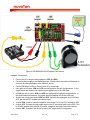
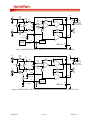
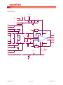
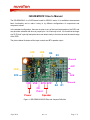
ISD-DEMO8101 User’s Manual The ISD-DEMO8101 is a SOP8 demo board for ISD8101 series. It is available to demonstrate basic functionality and to make it easy to try different configurations of components and component values. In the standard configuration, there are no pins on any of the input/output pads on the PCB, and may be either soldered with wires or jumper pins. As a fast way to test, it is found that the larger size "E-Z Hook" style clip lead probe wires can attach easily to the holes around the outside edge of the PCB. The picture below illustrates all the input controls and BTL speaker output. JCE JSE R6 R3 Ground ACP JON R10 ACN VDD VSS Power SPN SPP Ground R4 R1 CE Point Speaker Figure 1: ISD-DEMO8101EVB Pins and Jumpers Definition Sept, 2010 Rev 1.0 Page 1 / 8 Figure 2: ISD-DEMO8101EVB Possible Connections Hardware Connections: Connect an 8Ω or larger loading speaker to SPP and SPN. Connect a power supply to the related terminals. Please ensure the polarity of the power is correct to avoid any damages to the ISD8101 device. Connect CE either to VDD or Ground, and CE is active High Unity gain set of inputs: LPN and LPP are configured for low gain configurations. In the single ended use scenario, the signal may be applied only to the LPN input. A 20dB gain set of inputs: ACN and ACP are configured for high gain configurations. In the single ended use scenario, the signal should be applied only to the ACN input. Another set of high gain inputs, DCN and DCP, that have the same gain as for ACN and ACP, but that are DC coupled to the device input Jumper JON: install to cause the amplifier to be always "on" since CE is shorted to VDD. Jumper JCE: Connect the chip enable input to the CE connection point on the PCB. This is must be installed if an external CE control voltage will be used to control the device. Jumper JSE: Connect if the device is used in the "single ended" configuration. Sept, 2010 Rev 1.0 Page 2 / 8 Operations: Standalone Operations: Below are four common ways that parts such as the ISD8101 are used in audio circuits. To use this user guide, it is best to first identify which of these configurations most closely matches the desired application scenario. Best performance is always achieved by using the differential configuration, and when this can be used, difficult noise/pop/click issues can be most reduced. Figure 3: Single-Ended Design Controlled by Chip Enable. Lowest parts count using just one input, and an external controller manages the Chip Enable CE pin for best performance. i) Connect jumper JCE, and then CE depends on the CE point control voltage. Thus an external CE control voltage should be used to control the device. ii) Connect jumper JSE for single-ended input. iii) Connect power supply to VDD and ground to VSS. iv) Connect 8Ω (or larger) load speaker to SPP and SPN. v) Insert the input audio signal to either Unity Gain Input LPN (0dB gain configuration) or High Gain Input ACN (20dB gain configuration). Figure 4: Single-Ended Design, Always-On Case (Chip Enable tied to Vdd). Lowest parts count using just one input, but no external controller is available to manage the Chip Enable CE pin. The device is always enabled by connection of the Chip Enable pin directly to Vdd. i) Connect jumper JON, and thus CE is always ON. ii) Connect jumper JSE for single-ended input. iii) Connect power supply to VDD and ground to VSS. iv) Connect 8Ω (or larger) load speaker to SPP and SPN. v) Insert the input audio signal to either Unity Gain Input LPN (0dB gain configuration) or High Gain Input ACN (20dB gain configuration). Sept, 2010 Rev 1.0 Page 3 / 8 Application Schematic: Vdd Rb 55k R3 0 - 50k Vin INP - INV C2 0.1uF 8 Ra 5.5k 5 C6 0.01uF -1uF Vdd C1 value range: 10uF to 100uF 100uf is preferred 1 SPN + C1 Cbulk + 4 Rc 5.5k Re Rd 55k RL Rf VREF 6 C9 0.1uF-4.7uF - SPP 2 + CE V >1.1V = 7 Enabled External Controller Rg 40k Bias Generator Vss ISD8101 3 Figure 3: SINGLE-ENDED DESIGN CONTROLLED BY CHIP ENABLE CASE Vdd Rb 55k R3 0 - 50k Vin C6 0.01 - 1uF 5 C2 0.1uF 8 Ra 5.5k - INV INP Vdd 1 SPN + C1 Cbulk C1 value range: 10uF to 100uF 100uf is preferred + 4 Rc 5.5k Re Rd 55k RL Rf VREF Vdd 6 C9 0.1uf -4.7uF + R10 C10 SPP 2 CE V >1.1V = 7 Enabled Rg 40k Bias Generator Vss ISD8101 3 Figure 4: SINGLE-ENDED DESIGN, ALWAYS-ON CASE (CHIP ENABLE TIED TO Vdd) Sept, 2010 Rev 1.0 Page 4 / 8 Figure 5: Differential Input Design Controlled by Chip Enable. Differential inputs are used, and are best such as when filtering a PWM (Pulse Width Modulated) signal and handling other difficult signal input design requirements. An external controller manages Chip Enable. i) Connect jumper JCE, and then CE depends on the CE point control voltage. Thus an external CE control voltage should be used to control the device. ii) Connect power supply to VDD and ground to VSS. iii) Connect 8Ω (or larger) load speaker to SPP and SPN. iv) Insert the input audio signal to either Unity Gain Differential Inputs LPN and LPP (0dB gain configuration) or High Gain Differential Inputs ACN and ACP (20dB gain configuration). Figure 6: Differential Input Design, Always-On Case (Chip Enable tied to Vdd). Differential inputs are used, and are best such as when filtering a PWM (Pulse Width Modulated) signal and handling other difficult signal input design requirements. No external controller is available to manage the Chip Enable CE pin. The device is enabled at all times by connection of the Chip Enable CE pin directly to Vdd. i) Connect jumper JON, and thus CE is always ON. ii) Connect power supply to VDD and ground to VSS. iii) Connect 8Ω (or larger) load speaker to SPP and SPN. iv) Insert the input audio signal to either Unity Gain Differential Inputs LPN and LPP (0dB gain configuration) or High Gain Differential Inputs ACN and ACP (20dB gain configuration). Sept, 2010 Rev 1.0 Page 5 / 8 Vdd R1 50k Vinv C6 0.1uF Rb 55k R3 5 C5 0.01uF R7 - INV - INP + Vinp R4 50k Rc 5.5k R6 Re Rd 55k RL Rf VREF 6 - C9 0.1uF-4.7uF SPP 2 + CE V >1.1V = 7 Enabled External Controller Rg 40k C1 Cbulk C1 value range: 10uF to 100uF 100uf is preferred 1 SPN + 4 C2 0.1uF 8 Ra 5.5k R14 C7 0.1uF Vdd Bias Generator Vss ISD8101 3 Figure 5: DIFFERENTIAL INPUT DESIGN CONTROLLED BY CHIP ENABLE CASE Vdd R1 50k Vinv C6 0.1uF Rb 55k 5 R7 C5 0.01uF - INP + Vdd Rc 5.5k R6 C1 Cbulk C1 value range: 10uF to 100uF 100uf is preferred Re Rd 55k RL Rf VREF 6 C9 0.1uF-4.7uF - SPP 2 + R10 CE C10 1 SPN + 4 R4 50k - INV Vinp C2 0.1uF 8 Ra 5.5k R14 C7 0.1uF Vdd R3 V >1.1V = Enabled 7 Rg 40k Bias Generator Vss ISD8101 3 Figure 6: DIFFERENTIAL INPUT DESIGN, ALWAYS-ON CASE (CHIP ENABLE TIED TO Vdd) Sept, 2010 Rev 1.0 Page 6 / 8 EVB Schematic: TP TP 1 PWR2 1 PWR1 1 M2 1 M1 VDD1 TP TP TP PWR jumper 1 R11 VDD2 TP 1 0-ohm C1 100uF VSS1 TP VSS2 TP TP TP TP C3-NS 33pF C4-NS 10pF 1 DCN1 1 DCN2 1 ACN1 1 R8 R12-NS tINV R TP C2 0.1uF 1 TP ACN2 1 1 R C12-NS C 1uF 0-ohm LPN2 1 JSE jumper C8-NS 5 C C9 4.7uF LPP1 1 C14-NS 22pF JSE1 4 TP TP C7 R6 TP 2 SPP 1 TP SPP2 1 1 0-ohm 1uF 0-ohm ACP1 1 ACP2 1 C13-NS C C15-NS 22pF TP R9-NS TP 1 R13-NS R DCP1 1 JCE1 1 TP TP JON2 1 VDD 1 TP JON jumper JCE2 tCE 1 1 R10 TP TP JCE jumper DCP2 1 CE 1 TP tINP JON1 TP TP INP ISD8101 R TP 1 tGND 50k 1% TP R5 1 SPP1 7 R4 1 JSE2 LPP2 1 TP SPN2 Vref CE R INV SPN1 1 SPN 6 1 C5-NS C 1 VREF R14-NS R7-NS R TP U1 C11-NS 22pF TP 8 0-ohm VDD 50k 1% tVDD 1 VSS R3 3 C6 9 R2 GPAD R1 TPTP TP LPN1 1 TP TP 1 TP 2.2k C10-NS C Sept, 2010 Rev 1.0 Page 7 / 8 VERSION HISTORY VERSION DATE PAGE Rev. 1.0 Sept 30, 2010 all DESCRIPTION Initial Release Important Notice Nuvoton products are not designed, intended, authorized or warranted for use as components in systems or equipment intended for surgical implantation, atomic energy control instruments, airplane or spaceship instruments, transportation instruments, traffic signal instruments, combustion control instruments, or for other applications intended to support or sustain life. Furthermore, Nuvoton products are not intended for applications wherein failure of Nuvoton products could result or lead to a situation wherein personal injury, death or severe property or environmental damage could occur. Nuvoton customers using or selling these products for use in such applications do so at their own risk and agree to fully indemnify Nuvoton for any damages resulting from such improper use or sales. Sept, 2010 Rev 1.0 Page 8 / 8