1
ComputertechnikGmbH
ISA96 P7/106
Technical Description
Order Numbers:
404.258600.266 2
404.258600.300 8
404.258600.450 2
ISA96 P7/106 AMD-K6-2, 266MHz, Low Power
ISA96 P7/106 AMD-K6-2, 300MHz
ISA96 P7/106 AMD-K6-2, 450MHz
Your contact:
2000 by Janich & Klass Computertechnik GmbH, Wuppertal
22.05.00
Zum Alten Zollhaus 20 • 42281 Wuppertal • Germany
Tel: +49 (0)202 2708-0 • Fax: +49 (0)202 700625 • BBS: +49 (0)202 2708-191
Technical Description
Page 2
Rev. 1.2
ISA96 P7/106
(22.05.00)
Technical Description
Rev. 1.2
ISA96 P7/106
Table of Contents
1 Overview .......................................................................................................................... 7
2 Wiring Description............................................................................................................ 8
2.1
Logic Diagram.......................................................................................................... 8
2.2
Processor ................................................................................................................ 9
2.3
Chip Set................................................................................................................... 9
2.4
Main Memory ........................................................................................................... 9
2.5
Video Controller ....................................................................................................... 9
2.5.1 Video-I/O-Addresses ......................................................................................... 10
2.5.2 Memory Addresses ........................................................................................... 10
2.5.3 Operating Modes............................................................................................... 10
2.5.4 Flat Panel Type ................................................................................................. 11
2.5.5 Video-BIOS ....................................................................................................... 11
2.5.6 Driver-Software ................................................................................................. 11
2.6
Socket for PCI-Module........................................................................................... 11
2.7
128KByte SCRAM ................................................................................................. 12
2.8
Flash-Disk.............................................................................................................. 12
2.9
DiskOnChip ......................................................................................................... 12
2.10 Connecting the PS/2 Mouse .................................................................................. 13
2.11 USB Interfaces....................................................................................................... 13
2.12 EEPROM ............................................................................................................... 13
2.13 Watchdog .............................................................................................................. 14
2.14 Survey Component LM78 ...................................................................................... 14
2.15 I/O-Address Assignment ........................................................................................ 15
3 Fast Ethernet-PCI Module (Option) ................................................................................ 16
3.1
3.2
3.3
Status-LEDs........................................................................................................... 16
Software Drivers .................................................................................................... 17
Useful Hints for the Ethernet Module ..................................................................... 18
4 Jumpers & Switches....................................................................................................... 19
4.1
4.2
4.3
Core Voltage.......................................................................................................... 19
Clock Frequency.................................................................................................... 19
Deleting the Standard-CMOS-RAM ....................................................................... 20
5 Plug Assignment ............................................................................................................ 21
5.1
Bus Assignment in ISA96 Bus Systems................................................................. 21
5.2
Floppy Interface ..................................................................................................... 22
5.2.1 Connector Assignment of the Floppy Interface.................................................. 22
5.3
IDE-interfaces ........................................................................................................ 23
5.3.1 Connector Assignment of the Standard IDE Interface ....................................... 23
5.4
Serial Interfaces..................................................................................................... 24
5.5
Connector Assignment of the Parallel Interface ..................................................... 24
5.6
Monitor................................................................................................................... 25
5.7
Connector Assignment of the Keyboard Interface.................................................. 25
5.8
Plug for Speaker Connection ................................................................................. 26
5.9
Front Panel ............................................................................................................ 26
(22.05.00)
Page 3
Technical Description
Rev. 1.2
ISA96 P7/106
6 BIOS .............................................................................................................................. 27
6.1
Power-On-Self-Test ............................................................................................... 27
6.1.1 Beep-Codes ...................................................................................................... 27
6.1.2 Visual Messages on the Screen ........................................................................ 27
6.1.3 POST-Codes..................................................................................................... 29
6.2
Setup ..................................................................................................................... 33
6.3
BIOS Update.......................................................................................................... 48
7 Technical Data ............................................................................................................... 49
8 Environment Conditions ................................................................................................. 49
9 Position Print.................................................................................................................. 50
10
Appendix .................................................................................................................... 51
10.1 Good to Know ........................................................................................................ 51
10.1.1 External/Internal Floppy and IDE Drives ............................................................ 51
10.1.2 Requirements to 5V Supply............................................................................... 51
10.1.3 USB-BIOS-Extension ........................................................................................ 52
10.1.4 Problem: Interrupt Lines - Plug&Play................................................................. 52
Page 4
(22.05.00)
Technical Description
Rev. 1.2
ISA96 P7/106
Copyright
© 1999 Janich & Klass Computertechnik GmbH. All rights reserved. Printed in Germany.
The information contained in this documentation is the property of Janich & Klass
Computertechnik GmbH, Wuppertal. Neither receipt nor possession hereof confers or
transfers any right to reproduce or disclose any part of the contents hereof, without the prior
written consent of Janich & Klass.
Trademarks
All product names and logos are trademarks or registered trademarks of their representative
companies.
Disclaimer
The contents of this manual are checked for matching the described product. Deviations
cannot be excluded, so that we cannot give any guarantee for full accuracy. The details of
this manual are however regularly checked. Necessary corrections will be contained in the
subsequent revisions. We will be thankful for any improvement proposals.
Janich & Klass Computertechnik GmbH assume no liability for damages incurred directly or
indirectly from errors in this manual, omissions, or discrepancies between this manual and
the product.
Safety Hints
• This unit may not be used in any other way than described in this manual.
• Installation, putting into operation, and maintenance of this unit may exclusively be made
by qualified personnel. This personnel must be familiar with the warnings and hints of this
manual.
• Qualified personnel by means of this manual are persons who are familiar with
installation, mounting, putting into operation and operation of this unit and who have the
qualification fitting their tasks, like for example:
- Education and instructions, respectively the authorization to switch on/off, to ground,
and to tag current circuits and units resp. systems as per the actual standards of safety
technique.
- Education and instruction as per the actual standards of safety technique concerning
maintenance and use of appropriate safety equipment.
- Education in First Aid.
• Before you put this unit into a bus-rack, you have to check whether the required voltages
are available at the specific connector pins, and whether the required currents can be fed.
• Before exchanging any units, the sub-rack must be switched off.
• This unit contains electro-statically endangered components. Electro-static discharge
through the human body or similar must therefore by all means be avoided, for example,
by prior touch to grounded metal parts (water pipe, etc.). This is important specially before
exchanging the unit.
• You have to retighten all locking screws after every exchange.
• Protect this unit from moisture. By no means conductive matters or liquids may enter the
unit.
• Do not operate the unit at higher temperatures than stated in this description.
• Connected wires may not be subject to tension load.
(22.05.00)
Page 5
Technical Description
Rev. 1.2
ISA96 P7/106
• Do not expose the unit to strong magnet fields, for the danger of data loss from the hard
disk.
• The unit may not be exposed to strong vibrations, as they might destroy the hard disk.
• In case of a defective fuse, please by all means replace it with a new one of the same
type, as otherwise fire danger exists.
• This unit contains a lithium battery. ATTENTION! Explosion danger at inadequate battery
exchange. The battery may be replaced only with the same type, or with a type
recommended by Janich & Klass. Used batteries must be disposed according to legal
prescriptions.
• At visible damages of the unit, please return it to Janich & Klass for repair. (Each
unauthorized repair may lead to loss of the guarantee.)
• Do not try to repair this unit on your own. Please always address yourself to Janich &
Klass in case of eventual repair.
• Guarantee repair must always be made directly by Janich & Klass.
History
Revision
Date
Name
0.0
17.02.99
p.b
Preliminary Description
0.0
1.0
19.05.99
p.b
Adaptation to Hardware Rev. 1.0
1.0
1.1
17.08.99
p.b
Adaptation to BIOS Rev. 1.1
1.0
1.2
18.10.99
p.b
Net module added, new Appendix
1.0
Page 6
Modifications
HW-Revision
(22.05.00)
Technical Description
Rev. 1.2
ISA96 P7/106
1 Overview
For applications with highest demands to processor capacity and memory size, the ISA96
P7/106 has been developed. It is equipped with a "Socket 7"-compatible processor with a
clock frequency of actually up to 450MHz. The high data throughput is granted by, beside
the bus frequency of 100MHz, also by the Pipelined-Burst-Cache, the synchronous DRAM,
an AGP-VGA-controller, and by an PCI-IDE interface (Ultra-33 DMA). Different survey
components, connected by the SMBus network, guarantee high operating safety.
The Technical Data of the ISA96 P7/106 in Short:
• 64Bit Pentium-CPU, "Socket 7" compatible, clock frequency up to 450MHz, Bus
frequency up to 100MHz.
• AGP VGA with 2MByte EDO video memory and interface for flat panels (compatible to
ISA96 VGA/2).
• One DIMM socket for synchronous 64Bit-DRAM 16MByte up to 512MByte.
• 512KByte synchronous 64Bit-Pipelined-Burst L2-Cache.
• Licensed AWARD-BIOS and VGA-BIOS in a 256KByte EPROM.
• Two high performance PCI-IDE interfaces ("Ultra 33 synchronous DMA-Mode") of the
interfaces is occupied by the integrated 2,5" hard disk; you may connect one or two IDE
hard disks to the second interface.
• Floppy controller for 2 drives 1,44MByte.
• One AT-compatible multi-mode parallel-interface (ECP, EPP, PS/2, SPP).
• Three AT-compatible serial interfaces with 16 Byte FIFO. The interfaces can be
configured via exchangeable modules.
• Keyboard controller with mini-DIN female plug on the front panel.
• Connection for PS/2 mouse on the front panel.
• Two USB interfaces.
• LM78 for survey of temperatures, fan and supply voltages.
• Watchdog, can be disabled.
• Copy of CMOS-SETUP in the EEPROM.
• LED displays on the front panel: "RU", "HD" and "GP".
• Bootable Flash-Disk as option, with Flash File System, size 2 or 4MByte.
• Battery-buffered SRAM-Disk, size 128KByte.
• Operating temperature 5-60°C, relative humidity 10-90% non-condensing.
• Power consumption 5V/4A; 12V/0,3A without serial modules and options.
• Available for the ISA96 Bus.
(22.05.00)
Page 7
Technical Description
Rev. 1.2
ISA96 P7/106
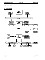
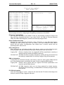
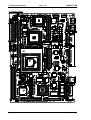
2 Board Description
2.1 Logic Diagram
Page 8
(22.05.00)
Technical Description
Rev. 1.2
ISA96 P7/106
2.2 Processor
For the processor, the ISA96 P7/106 offers a so-called "Socket7", so that all usual Socket7compatible processors with an I/O voltage of 3,3V and a Core voltage of 1,8V...3,5V can be
inserted. For exchanging the processor, you first must dismantle the heat sink. Then, the
locking lever of the Socket7 can be set vertical. The processor is now lose and can be
exchanged. Please notice when inserting the new processor that the angled edge of the
processor fits the angled edge of the socket. At correct alignment, the processor must drop
into the socket on its own. If you use force for this process, you risk damaging the processor
and the socket! The locking lever is then pressed downwards again, and the heat sink can
be mounted with just a few heat-conducting paste.
2.3 Chip Set
At modern (industrial) PC's, the majority of the functionality is integrated in the so-called chip
set. The ISA96 P7/106 utilizes the chip set "Aladdin V" from Acer Labs Inc. (ALI), which
consists of the two chips M1541 and M1543C. The M1541 connects the processor to the
main memory and to the internal PCI-Bus. The M1543C connects the internal PCI-Bus to the
integrated periphery and the ISA96-Bus. You can get the actual driver for the chip set either
directly from Janich & Klass, or from ALI (www.acerlabs.com).
2.4 Main Memory
The ISA96 P7/106 has a socket for a 168pin SDRAM module with memory sizes from
16MByte to 512MByte. For Bus frequencies up to 66MHz (refer Chapter "Clock Frequency"),
PC66 modules may be used. For Bus frequencies above 66MHz, it is indispensable to use
PC100 modules, as otherwise the functionality of the ISA96 P7/106 can not be guaranteed.
For assembly of the main memory, the 168pin SDRAM modules must be turned until their
two notches match with toes of the socket. The module is carefully inserted into the socket
from above and is pressed down evenly with little force. The two locking hooks must click
audibly. Inserting with wrong poles is possible only with strong force and will destroy the
socket or the module!
The BIOS will automatically recognize the size of the assembled SDRAM modules.
2.5 Video Controller
The video controller of the ISA96 P7/106 is built up with a 69000 from Chips&Technologies.
This video controller has already 2MByte integrated video-SDRAM; it works on the AGP-Bus
of the chip set with a clock frequency of 66MHz and can support nearly all actually available
flat panels. The connector for an analog monitor is already placed on the main board. If a flat
panel shall be used, a driver module to match the panel must still be assembled.
(22.05.00)
Page 9
Technical Description
Rev. 1.2
ISA96 P7/106
2.5.1 Video-I/O-Addresses
3B0h - 3B3h
3B4h
3B5h
3B6h - 3B9h
3BAh
3BBh - 3BFh
3C0h
3C1h
3C2h
3C3h
3C4h
3C5h
3C6h
3C7h
3C8h
3C9h
3CAh
3CBh
3CCh
3CDh
3CEh
3CFh
3D0h
3D1h
3D2h
3D3h
3D4h
3D5h
3D6h
3D7h
3D8h - 3D9h
3DAh
3DBh - 3DFh
CRTC Index (MDA Emulation)
CRTC Data Port (MDA Emulation)
reserved
Input Status Register 1 (ST01) / Feature Control Register (FCR)
reserved
Attribute Controller Index
Attribute Controller Data Port
Input Status Register 0 (ST00) / Output Register (MSR)
reserved
Sequencer Index
Sequencer Data Port
Color palette Mask
Color palette State / Color Palette Read Mode Index
Color palette Write Mode Index
Color palette Data Port
Feature Control Register (FCR)
reserved
Misc. Output Register (MSR)
reserved
Graphics Controller Index
Graphics Controller Data Port
Flat Panel Extensions Index
Flat Panel Extensions Data Port
Multimedia Extensions Index
Multimedia Extensions Data Port
CRTC Index (CGA Emulation)
CRTC Data Port (CGA Emulation)
Configuration Extensions Index
Configuration Extensions Data Port
reserved
Input Status Register 1 (ST01) / Feature Control Register (FCR)
reserved
2.5.2 Memory Addresses
A0000h - AFFFFh
B0000h - BFFFFh
B8000h - B8FFFh
A0000h - BFFFFh
Video memory, as per image format
C0000h - CBFFFh
48KByte Video-BIOS
2.5.3 Operating Modes
The video controller supports the following operating modes:
•
•
•
display image on an analog monitor
display image on monochrome- and color-LCD, EL panel or Plasma panel
simultaneous isplay on both monitor and flat panel
At system start it is checked whether an analog monitor is connected. If so, graphics are
displayed on it. If no monitor is connected, the graphics are displayed on the flat panel.
Page 10
(22.05.00)
Technical Description
Rev. 1.2
ISA96 P7/106
The simultaneous operating mode is not restricted to any special graphics formats, but is
possible with nearly all graphics formats.
At simultaneous mode (CRT monitor and flat panel), please notice that both panel types
must work with the same resolution. So, it is not possible to set the CRT monitor to a
resolution of 800x600, if the connected flat panel works with 640x480 pixels resolution.
2.5.4 Flat Panel Type
If a flat panel shall be connected to the ISA96 P7/106, you have to set the type of panel in
advance at rotary switch SW1. Actually, the following panel types can be set:
SW1
Display Type
F
Mono, 640x480, 8Bit, Dual Scan
E
FSTN, 640x480, 16Bit, Dual Scan
D
TFT, 640x480, 18Bit
C
TFT, 640x480, 9Bit
3
TFT, 1024x768, 2x18Bit
Attention: This setting is critical! A wrong setting may lead to destruction of the
connected flat panel!
2.5.5 Video-BIOS
The BIOS of the video controller is fully compatible to the Standard IBM VGA BIOS and the
interrupt 10h video service functions. These interrupt 10h standard functions are described
in detail in diverse publications and are no subject of this description.
All BIOS extensions which surpass the VGA Standard are documented in the separate BIOS
Description "BIOS_69.PDF". Mainly, the BIOS functions are described, with which one can
switch between the different display modes (only flat panel, only analog monitor, or
simultaneous operation).
2.5.6 Driver-Software
Device drivers for the video controller of the ISA96 P7/106 are available for Windows-95,
Windows-98 and Windows-NT 4.0. Please get the actual driver either directly from Janich &
Klass, or from Chips & Technologies (www.chips.com).
2.6 Socket for PCI-Module
The header S27 is a position for an optional PCI module (for example, Fast-Ethernet). The
actual Janich & Klass Price List will tell you which PCI modules are actually available.
(22.05.00)
Page 11
Technical Description
ISA96 P7/106
Rev. 1.2
2.7 128KByte SCRAM
Placed on the ISA96 P7/106, in addition to the SDRAM main memory, is a 128KByte static
CMOS-RAM (SCRAM), which contents can be buffered by the internal Lithium battery.
The SCRAM can be used in two different ways:
linear: The SCRAM is switched into the memory area, either complete, or partly directly
between 0D0000h and 0EFFFFh. The required size and start address can be set in the
BIOS-Setup on page "Special Features Setup" under menu item "On-Board Static RAM".
Surely, the set address area may not be assigned by other cards.
switched: In this operating mode, the SCRAM is divided to blocks of 16KByte each, of
which always only one block at a time is switched into the memory address area between
0CC000h and 0EFFFFh. Via an I/O port, the number of the block to be switched in can be
set. The start address of the 16KByte area can be set in BIOS-Setup on page "Special
Features Setup" under menu item "On-Board Flash-Disc". This operating mode is
compatible to the EPROM-Disk of the former ISA96 CPU cards, so that, for example, a
battery-buffered 128KByte virtual hard disk can be switched in by using the MSDOS-driver
ECDISK.SYS.
If the SCRAM shall be buffered by the battery, jumper J6 must be set. If this is not desired,
this jumper should not be set, in order to prolong the lifetime of the battery.
2.8 Flash-Disk
Optionally, the ISA96 P7/106 is assembled with 2MByte or 4MByte Flash-EPROM, with
which you can build an up to 4MByte large virtual hard disk drive (Flash-Disk).
The Flash-EPROM is switched in as 16KByte large block in the memory address area
between 0CC000h and 0EFFFFh. The start address of the block can be set in BIOS-Setup
on page "Special Features Setup" under menu item "On-Board Flash-Disc". Certainly, the
set address area may not be assigned by other cards. Furthermore, the Flash-Disk still
requires two Bytes in the I/O address area, whose start address can also be set in BIOSSetup.
For creating the required file system on the Flash-EPROM, you will require the Janich &
Klass Flash-File-System (please refer the separate Description). Then, the Flash-Disk is
bootable also with this Flash-File-System.
2.9 DiskOnChip
A Flash-Disk-Chip from the company M-Systems ("DiskOnChip ") can be plugged into
socket EP1. This chip already contains a Flash-File-System, it is bootable, and it works with
all usual operating systems. Actually, this chip is available in sizes between 2MByte and
114MByte.
The Flash-Disk-Chip in socket EP1 is switched in as 16KByte block in the memory address
area between 0CC000h and 0EFFFFh. The start address of the block can be set in BIOSSetup on page "Special Features Setup" under menu item "On-Board Socket EP1".
Page 12
(22.05.00)
Technical Description
Rev. 1.2
ISA96 P7/106
Installation:
1. Switch your computer system off and take out the ISA96 P7/106.
2. Carefully insert the DiskOnChip into the socket marked "EP1". Attention: The point on
the chip (Pin 1) must show in the same direction as the edge in the socket!
3. Put the ISA96 P7/106 back into the computer system and switch on your system again..
4. During the boot procedure, watch for messages from the DiskOnChip.
5. If the DiskOnChip is the only mass memory in your system, it will become available after
booting as hard disk C:
6. If, besides the DiskOnChip, further hard disks exist in the system, it will be available after
booting as the last hard disk, if not configured differently (refer "DiskOnChip 2000 Utilities
User Manual").
7. If the DiskOnChip shall be able to boot, please note the following:
• Copy the operating system on the DiskOnChip, for example with the MSDOS
command "sys d:".
• The DiskOnChip should be the only bootable drive in the system, respectively it should
be configured as first drive with the utility "DUPDATE".
2.10 Connecting the PS/2 Mouse
Built into the front panel of the ISA96 P7/106 is a 6pin mini-DIN female plug where a PS/2
mouse can be connected. For using this interface, the menu "PS/2 Mouse Function Control"
must be "enabled" in BIOS-Setup on page "BIOS Features Setup". Furthermore, in the setup
page ”Special Features Setup”, the menu item "IRQ12 Routing" must be set to "PS/2Mouse". The interrupt line IRQ12 is then assigned by the PS/2 mouse controller and no
longer available on the ISA96-Bus!
2.11 USB Interfaces
The front panel of the ISA96 P7/106 offers two equivalent USB interfaces (Universal Serial
Bus) for connecting periphery units. The USB interfaces meet the USB Specification 1.1 and
therefore allow transmission rates of 12Mbit/s. USB units are "hot-plug"-able, i.e. they may
be plugged on and -off during operation of the P7/106. For operating USB units, certainly an
operating system is required which supports the USB interfaces, like e.g. Windows 98.
2.12 EEPROM
The ISA96 P7/106 also features a 256Byte EEPROM. It usually contains a 1:1 image of the
Setup parameters which are stored in the Standard-CMOS-RAM. Should the battery fail, the
data in the Standard-CMOS-RAM become invalid. The BIOS of the ISA96 P7/106 will then
read the parameters which were stored latest in the EEPROM, and will write them back into
the Standard-CMOS-RAM. This way, the computer can still boot after a battery failure
without user action. In such a case, however, date and time are wrong and must
correspondingly be corrected.
In order to prevent that in case of invalid CMOS-RAM data automatically the contents of the
EEPROM are copied into the CMOS-RAM, set Jumper J4 (this will make sense only in the
rare case that the EEPROM holds senseless data). Then, all adjustments in the Setup have
to be repeated and must again be stored in the CMOS-RAM. Afterwards, Jumper J4 can be
removed again.
(22.05.00)
Page 13
Technical Description
Rev. 1.2
ISA96 P7/106
2.13 Watchdog
The ISA96 P7/106 features a Watchdog that creates a hardware Reset if it is not triggered
periodically by the running program within a certain time. This can considerably improve the
reliability of the whole system.
In the BIOS-Setup, the page "Special Features Setup" allows to set different trigger periods
between 250ms and 32s. The Watchdog can also be disabled completely. To allow the
system to boot at all, the Watchdog becomes active only after it was triggered for the first
time.
Triggering the Watchdog:
As already mentioned, the Watchdog becomes active only when it is triggered for the first
time. Triggering is affected for 16Bit-operating systems (MSDOS, for example) by calling the
BIOS interrupts 0AFh, where the AH register must be zero. Please read the "Description of
the BIOS Expansions " for ISA96 P7/10x.
32Bit operating systems (Windows 9x, NT) require a specific driver software from Janich &
Klass.
2.14 Survey Component LM78
For surveying the supply voltages, the temperatures, and the fan, the hardware monitor
LM78 from National Semiconductors was integrated on the ISA96 P7/106. By using the
drivers available from Janich & Klass (MSDOS, Windows9x, Windows-NT), you can query
the following measuring readings:
• Supply voltages:
• Temperatures:
• Fan:
Core voltage, 3.3V, 5V, 12V and -12V
Card temperature and CPU temperature
Propeller rotation frequency
Furthermore, you can set limit values for each measuring. When surpassed, the LM78 can
generate an NMI. The user program is thus enabled to take measures to prevent the total
system from damage.
Page 14
(22.05.00)
Technical Description
Rev. 1.2
ISA96 P7/106
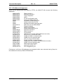
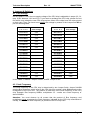
2.15 I/O-Address Assignment
Within the I/O address area from 0000h to FFFFh, the ISA96 P7/106 occupies the following
addresses:
0000h-000Fh
0020h-0021h
0040h-0043h
0048h-0050h
0050h-0053h
005Ch-005Fh
0060h
0061h
0064h
0070h-0071h
0080h
0080h-008Fh
0092h
00A0h-00A1h
00C0h-00DEh
00F0h-00F1h
01F0h-01F7h
0278h-027Fh
02E8h-02EFh
02F8h-02FFh
0378h-037Fh
03E8h-03EFh
03F2h-03F7h
03F8h-03FFh
0481h-048Bh
04D0h-04D1h
0CF8h-0CFCh
DMA controller 1
Interrupt controller 1
Timer component
LM78
P7/106 configuration port
Front panel diagnosis LCD
Keyboard controller data port
System status bits (Port B)
Keyboard controller command port
Real time clock & CMOS-RAM
Diagnosis display
DMA-Page-Register
System status bits (Port A)
Interrupt controller 2
DMA controller 2
Co-processor
Hard disk (if an ISA96 FILECARD does not exist)
LPT2 (if LPT1 on external card)
COM4 (if COM2 on external card)
COM2 (if not on external card)
LPT1 (if not on external card)
COM3 (if COM1 on external card)
Floppy-Disk (if an ISA96 FILECARD does not exist)
COM1 (if not on external card)
DMA-High-Page-Register
Interrupt controller 1/2
PCI configuration port
Furthermore, still those I/O-addresses are assigned which were selected during Setup for
the additional functions (COM3, EPROM-Disk).
(22.05.00)
Page 15
Technical Description
Rev. 1.2
ISA96 P7/106
3 Fast Ethernet-PCI Module (Option)
The Janich & Klass Fast Ethernet-PCI Module "P7 Net Module 10/100Base-TX” can be
mounted on the Onboard-PCI slot of the P7/106. This Fast-Ethernet card for the P7/106 is
equipped with the controller AM79C973 from AMD. It supports 10Base-T and 100Base-TX
networks. The UTP female plug for connecting a Standard-Twisted-Pair network cable can
be reached via the front panel.
General Features
•
Fast Ethernet controller AM79C973 with 32bit PCI-Bus interface
•
Integrated 10Base-T and 100Base-TX interface
•
Auto negotiation for 10Base-T and 100Base-Tx respectively semi and full duplex
•
Meats the requirements as per IEEE/ANSI 802.3
•
Full duplex operation at 10MBd/100MBd
•
12KByte chip-internal FIFOs for Rx and Tx
•
3 LEDs on the front panel for checking the network activities
•
EEPROM for non-volatile storage of user-specific settings
•
Software-compatible to components from the AMD Pcnet family
•
Ample driver software PCnet Family for nearly all platforms.
3.1 Status-LEDs
The network adapter controls 3 yellow LEDs (LN1, LN2, LN3), that are found on the front
panel below the network female plug. These LEDs can display status information about
condition and activity of the networks and controllers. The factory settings are as follows:
LN1: Link Integrity. This LED lights at trouble-free network link (therefore constantly during
normal operation).
LN2: Transmit Status. This LED lights at send activity of the network controller.
LN3: 100Base-TX. The LED is on, when the adapter works in 100MBaud mode.
Otherwise, the adapter is in 10Base-T mode. Recognition of and switch-over to the
actual network type is affected automatically.
The function assignment of the LEDs can partly be set by means of the network drivers
(depending on driver and platform). During driver installation under Windows, for example,
also values for LED0 up to LED3 can be set. Here correspond LED0 = LN1, LED1 = LN2,
LED2 = LN3, and LED3 is not realized on the network adapter.
We recommend to not alter these settings! First, the drivers (at least for now) do offer
some meaningful configurations not, and secondly some drivers will, at such an alteration,
remanently rewrite the internal configuration of the network controller, causing severe
problems, as we experienced ourselves.
If it still seems to be required to modify the LED configuration, the following information will
be useful. The LED configuration is displayed during the driver setting (actually) in form of an
integer value per LED. The meaning of some interesting bits of this value is listed below:
Bit0=1:
Collision Status. The LED lights, when collisions are remarked on the network.
Bit2=1:
Receive Status. The LED lights during receiving activity on the network.
Page 16
(22.05.00)
Technical Description
Rev. 1.2
ISA96 P7/106
Bit4=1:
Transmit Status. The LED lights during sending activity of the controller.
Bit5=1:
Receive Match Status. The LED lights, when the controller receives protocols
to its (node) address.
Bit6=1:
Link Status. The LED lights at a trouble-free network link (therefore constantly
at normal operation).
Bit7=1:
Pulse Stretcher. If this Bit is 1, the lighting of the LED is prolonged to get
visible to the eye also at short activities.
Bit8=1:
Full Duplex Link Status. The LED lights, when the controller is in Full-Duplex
operation.
Bit12=1:
100BMd Enabled. The LED lights, when the controller works in 100MBaud
mode.
All bits can be combined with each other, so that, for example, the value 0094h means that
the LED lights at sending and receiving activity, where the signal is prolonged.
The basic setting stated above corresponds to the following values:
LN1 = 00C0h,
LN2 = 0090h,
LN3 = 1080h.
3.2 Software Drivers
Software drivers from AMD for the P7 Net modules are available on request, free of charge.
They cover a majority of usual operating systems.
Please find the most actual drivers on the Web Page of AMD:
http://www.amd.com
In their actual Version 4.51, the "Pcnet Family Driver” contain drivers for the following
operating systems respectively platforms:
•
•
•
•
•
•
•
•
•
•
•
•
•
•
•
•
•
•
•
DOS
Netware Server AHSM
Netware Server CHSM
Netware Workstation
OS/2
PCNFS
SCO UNIX OpenServer and ODT
SCO UnixWare
SUN Solaris
Windows 3.1
Windows 3.11
Windows 9x
Windows NT 3.50
Windows NT 3.51
Windows NT 4.0
Windows CE 2.1
Windows 2000 Beta
VxWorks Driver
Packet Driver
(22.05.00)
Page 17
Technical Description
Rev. 1.2
ISA96 P7/106
3.3 Useful Hints for the Ethernet Module
Key word Auto Negotiation:
The network controller supports Auto Negotiation related to Half and Full Duplex switch-over,
and related to 10Base-T and 100Base-TX switch-over. This means the following: The
network controller periodically informs the other network members via so-called Link-Pulse
protocols, containing information about its capabilities, especially supported modes and
possible Baud-rates. In reaction, it evaluates the Link-Pulse protocols of all other members
at a network segment. This way, the largest common denominator of all segment members
is evaluated, and this one is automatically set. For the user, the necessity is voided to
manually set the network configuration in these items.
This network controller works in 100Base-TX and 10Base-T networks, both in Half and Full
Duplex mode, without the need for any settings.
Key word Driver Installation:
During installation of the network drivers for Windows 9x (and possibly also for other
platforms) the user is requested at some driver versions to make driver settings concerning
I/O address, DMA channel and IRQ line. These settings must not and should not be made,
as the network controller is a PCI component, able for Plug&Play like all other PCI
components. This means that the resource administration of such components concerning
I/O and memory addresses, DMA and interrupt lines is affected dynamically by the BIOS of
the P7/106. (It can eventually still be modified later by the operating system.)
After installation of the network drivers and a re-start of the system, these setting
possibilities for driver configuration are (correctly) no longer available.
Furthermore, the user is often asked during driver installation for type and make of his
network card, and a corresponding dialog box is displayed. Please select the manufacturer
"Advanced Micro Devices” respectively "AMD” and the card type "AMD PCNET Family
Ethernet Adapter (PCI)” (or a similar denomination which contains the term "PCI”.)
Page 18
(22.05.00)
Technical Description
ISA96 P7/106
Rev. 1.2
4 Jumpers & Switches
4.1 Core Voltage
On the ISA96 P7/106, the core supply voltage of the CPU chip is adjustable in steps of 0,1Vresp. 0,05V between 1,8V and 3,5V. If you want to exchange the CPU chip, please find out
first which core voltage the new CPU chip requires. Most of the chips have this value printed
on their case. Then, you have to set exactly this voltage by means of the Jumper field S5 as
per the following table:
S5
e d c b a
CPU
Core Voltage
S5
e d c b a
CPU
Core Voltage
ooooo
2,0V
ýoooo
-
ooooý
2,1V
ýoooý
-
oooýo
2,2V
ýooýo
-
oooýý
2,3V
ýooýý
-
ooýoo
2,4V
ýoýoo
-
ooýoý
2,5V
ýoýoý
-
ooýýo
2,6V
ýoýýo
-
ooýýý
2,7V
ýoýýý
-
oýooo
2,8V
ýýooo
-
oýooý
2,9V
ýýooý
-
oýoýo
3,0V
ýýoýo
1,80V
oýoýý
3,1V
ýýoýý
1,85V
oýýoo
3,2V
ýýýoo
1,90V
oýýoý
3,3V
ýýýoý
1,95V
oýýýo
3,4V
ýýýýo
2,00V
oýýýý
3,5V
ýýýýý
2,05V
In this Table, o means: "Jumper not set", and ý "Jumper is set".
4.2 Clock Frequency
The clock frequency of the CPU chip is determined by two Jumper fields: Jumper field S2
sets the Bus frequency, which is fed to the CPU chip from outside, while S14 determines the
multiplicator of the CPU core. The product of both then is the clock frequency of the CPU
chip. Example: Bus frequency 66MHz, multiplicator 3,5 - results as a clock frequency of
about 300MHz.
Attention: You must observe by all means that the product of Bus frequency and
multiplicator never surpasses the clock frequency indicated by the CPU chip manufacturer!
Usually, this maximum clock frequency is printed on the CPU chip case.
(22.05.00)
Page 19
Technical Description
ISA96 P7/106
Rev. 1.2
The following table illustrates the meaning of jumper fields S2 and S14:
S2c
S2b
S2a
Bus-Frequency
S14c
S14b
S14a
Multiplicator
o
o
o
100,0 MHz
o
o
ý
2,0
o
o
ý
95,3 MHz
o
ý
ý
2,5
o
ý
o
83,3 MHz
o
ý
o
3,0
o
ý
ý
75,0 MHz
o
o
o
3,5
ý
ý
o
66,8 MHz
ý
o
ý
4,0
ý
ý
ý
60,0 MHz
ý
ý
ý
4,5
ý
ý
o
5,0
ý
o
o
5,5
In this table, o means ”Jumper not set", and ý "Jumper is set".
4.3 Deleting the Standard-CMOS-RAM
All parameters that can be changed via the BIOS-Setup are stored in the Standard CMOS
RAM. After switching the computer off, they are buffered by the battery. Should these data
once be modified uncontrolled, for example, by a program, it may happen that the ISA96
P7/106 will not boot correctly. In such cases, Jumper J5 must be set at switched-off
computer, and be removed again after about 10 seconds. The contents of the Standard
CMOS RAM is then declared invalid. The BIOS will then use the default values stored either
in the EEPROM or in the EPROM.
Page 20
(22.05.00)
Technical Description
ISA96 P7/106
Rev. 1.2
5 Connector Assignments
5.1 Bus Assignment in ISA96 Bus Systems
Attention: The ISA96 P7/106 can be used only in systems with ISA96 Bus!
(22.05.00)
a
b
c
1
GND
/MASTER
/IOCHCK
1
2
RESET
SD15
SD7
2
3
+5V
SD14
SD6
3
4
IRQ9
SD13
SD5
4
5
/MEMR
SD12
SD4
5
6
DRQ2
SD11
SD3
6
7
-12V
SD10
SD2
7
8
/0WS
SD9
SD1
8
9
+12V
SD8
SD0
9
10
GND
/SBHE
IOREADY
10
11
/SMEMW
LA23
AEN
11
12
/SMEMR
LA22
SA19
12
13
/IOW
LA21
SA18
13
14
/IOR
LA20
SA17
14
15
/DACK3
LA19
SA16
15
16
DRQ3
LA18
SA15
16
17
/DACK1
LA17
SA14
17
18
DRQ1
/DACK7
SA13
18
19
/REF
DRQ7
SA12
19
20
CLOCK
/DACK6
SA11
20
21
IRQ7
DRQ6
SA10
21
22
IRQ6
/DACK5
SA9
22
23
IRQ5
DRQ5
SA8
23
24
IRQ4
/DACK0
SA7
24
25
IRQ3
DRQ0
SA6
25
26
/DACK2
/MEMCS16
SA5
26
27
TC
/IOCS16
SA4
27
28
BALE
IRQ15
SA3
28
29
+5V
IRQ14
SA2
29
30
OSC
IRQ12
SA1
30
31
/MEMW
IRQ11
SA0
31
32
GND
IRQ10
GND
32
Page 21
Technical Description
ISA96 P7/106
Rev. 1.2
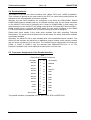
5.2 Floppy Interface
The ISA96 P7/106 has an interface for one or two floppy drives 3,5" (1,44MByte). Only a
34pole flat ribbon cable is required to connect the 34pin header row S24 to the floppy
drive(s).
This cable is to be made as follows:
The length depends on the mechanical composition of the computer, it should however not
exceed 46cm. A 34pole female plug is mounted on the CPU-sided end. About 10cm before
the other end, there is a 34pin direct plug connector. This is the connector for the second
drive. Behind this plug, wires 10 and 16, 11 and 15, and 12 and 14 are interchanged and
connected to a second 34pole direct plug, which is the plug for the first drive. If 3.5" drives
shall be used, please foresee 34pole female plugs instead the 34pole direct plug connectors.
Attention: Before using newly installed drives, the user has to change the floppy type in the
BIOS-Setup.
Attention: If a second floppy controller exists on the ISA96-Bus (e.g. Filecard, FD-Card), the
floppy controller on the ISA96 P7/106 must be disabled manually in the Setup!
5.2.1 Connector Assignment of the Floppy Interface
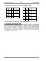
S24
34pin Header Row
Page 22
GND
1
2
RWC/RPM
GND
3
4
GND
5
6
GND
7
8
/INDEX
GND
9
10
/MOTOR ON 1
GND
11
12
/DRIVE SELECT 2
GND
13
14
/DRIVE SELECT 1
GND
15
16
/MOTOR ON 2
GND
17
18
/DIR
GND
19
20
/STEP
GND
21
22
/WDATA
GND
23
24
/WGATE
GND
25
26
/TRACK 0
GND
27
28
/WRITE PROTECT
GND
29
30
/RDATA
GND
31
32
/HEAD SELECT
GND
33
34
/DISK CHANGE
(22.05.00)
Technical Description
ISA96 P7/106
Rev. 1.2
5.3 IDE-interfaces
The ISA96 P7/106 has two high performance PCI-IDE interfaces, which also support the
"Ultra 33 synchronous DMA-Mode" at up to 33Mbytes/sec.
The first (primary) IDE-interface at header row S20 is reserved for a 2,5" hard disk. This hard
disk is mounted on the ISA96 P7/106 and connected via flat ribbon cable.
The second (secondary) IDE-interface is available at the 40pin header row S21. Here, one or
two IDE drives (hard disks, CD-ROM's) can be connected via a 40pole flat ribbon cable.
When using two hard disks, one of them must be configured as Master, the other as Slave.
Please take details from the Technical Descriptions of the hard disks.
Hint: Before using newly installed IDE drives, the user must first adjust the actually used
hard disk types and their operating modes in the Setup.
Attention: If a second IDE controller exists on the ISA96-Bus (for example Filecard, HDCard), the corresponding internal IDE controller (primary or secondary) on the ISA96 P7/106
must be manually disabled in the Setup!
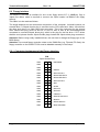
5.3.1 Connector Assignment of the Standard IDE Interface
S21
40pin Header Row
(22.05.00)
/RESET
1
2
GND
SD7
3
4
SD8
SD6
5
6
SD9
SD5
7
8
SD10
SD4
9
10
SD11
SD3
11
12
SD12
SD2
13
14
SD13
SD1
15
16
SD14
SD0
17
18
SD15
GND
19
20
DRQ
21
22
GND
/IOW
23
24
GND
/IOR
25
26
GND
IORDY
27
28
/DACK
29
30
IRQ15
31
32
SA1
33
34
SA0
35
36
SA2
/CS0
37
38
/CS1
/HDLED
39
40
GND
GND
Page 23
Technical Description
ISA96 P7/106
Rev. 1.2
5.4 Serial Interfaces
The ISA96 P7/106 has two serial interfaces with 16Byte FIFO each (16550 compatible).
Their controller is placed on the main board of the CPU unit, while the according drivers are
displaced to two exchangeable serial driver modules.
Normally, the two serial interfaces are configured in the Setup as COM1/COM2. Should
COM1/COM2 however already exist on an external interface card, the two serial interfaces
on the ISA96 P7/106 must be manually set in Setup as COM3/COM4. In both cases, the
serial interfaces on the ISA96 P7/106 assign interrupt lines INT4 and INT3! Should COM1...
COM4 already exist on external interfaces cards, the two serial interfaces on the ISA96
P7/106 must totally be disabled. Also, no further interrupt lines will be assigned.
Please take closer details of the serial driver modules from their according Technical
Descriptions. The actual Janich & Klass Price List will advise you which serial driver modules
are actually available.
Optionally, the ISA96 P7/106 is also available with a third assembled serial interface. The
drivers for this interface are placed on an additional plug-on module, which usually contains
also the driver component for a flat panel. The interface can be configured in the Setup as
COM1...4, COM7 or COM8, it can use interrupt lines IRQ3/4/5/7/10/11/12, or 15. The
interface is available only via an additional module (refer our Price List).
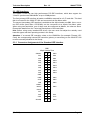
5.5 Connector Assignment of the Parallel Interface
S17
25pole Sub-D Female Connector
/STROBE
1
DATA0
2
DATA1
3
DATA2
4
DATA3
5
DATA4
6
DATA5
7
DATA6
8
DATA7
9
/ACK
10
BUSY
11
PE
12
SELECTED
13
14
/AUTOFEED
15
/ERROR
16
/INIT
17
/SELECT
18
GND
19
GND
20
GND
21
GND
22
GND
23
GND
24
GND
25
GND
The parallel interface is compatible to ECP, EPP, PS/2, SPP and IEEE1284.
Page 24
(22.05.00)
Technical Description
ISA96 P7/106
Rev. 1.2
5.6 Monitor
You can connect an analog monitor to the ISA96 P7/106 via the VGA-compatible 15pole HDfemale plug on the front panel. The following table shows the pole assignment:
S11
15pole Sub-HD Female Connector
1
Red
75Ω 0,7V
2
Green
75Ω 0,7V
3
Blue
75Ω 0,7V
4
-
5
Digital-GND
6
Analog-GND
7
Analog-GND
8
Analog-GND
9
-
10
Digital-GND
11
-
12
DDC-Data
TTL
13
HSYNC
TTL
14
VSYNC
TTL
15
DDC-Clock
TTL
5.7 Connector Assignment of the Keyboard Interface
Built into the front panel of the ISA96 P7/106 is a 6pole mini-DIN female connector where an
MF2-compatible keyboard can be connected. The keyboard connection is also available at
connector J2 on the main board. This connector has the following pin assignment:
1 CLOCK
4 GND
5
4
3
2
1
5 +5V
J2
2 DATA
3 N.C.
You can connect a key switch to the two-pin header J3 for locking the keyboard. As soon as
the switch closes, the keyboard controller will accept no further enters. This way, the
computer can be secured against non allowed usage.
(22.05.00)
Page 25
Technical Description
ISA96 P7/106
Rev. 1.2
5.8 Plug for Speaker Connection
Any usual speaker of 4...16 Ohm or a Piezo buzzer can be connected to the 4pin header row
S26.
S26
4pin Header Row
1
2
SPEAKER
3
4
GND
+5V
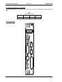
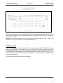
5.9 Front Panel
RU HD GP
USB
2
1
Ethernet
COM1
LN3 LN2 LN1
LPT1
VGA COM2
Reset
Mouse
Keyboard
Page 26
(22.05.00)
Technical Description
Rev. 1.2
ISA96 P7/106
6 BIOS
6.1 Power-On-Self-Test
After switching on the ISA96 P7/106, the BIOS effects a self test, the so-called "POST" =
Power-On-Self-Test. Eventual errors during this self test will be indicated either by beep
codes, or on the screen. An error message may be followed by the query to press the key
<F1> to continue, or <DEL> to get into Setup.
Furthermore, special POST codes are put out on the ISA96-Bus to I/O-address 80h, which
illustrate the process of the self test. If your ISA96 P7/106 is equipped with an LCD panel,
these POST codes will be displayed there, too.
6.1.1 Beep-Codes
Actually, the BIOS has only one single beep code. This code indicates that a video error has
happened and that the BIOS can not initialize the panel to indicate further information.
This beep code consists of one single long beep, followed by two short ones.
6.1.2 Visual Messages on the Screen
"BIOS ROM checksum error - System halted"
The checksum of the BIOS codes in the BIOS-Flash-EPROM is invalid. This means that
the BIOS code may be defective. Please address yourself to the Janich & Klass service
for exchange of the BIOS chip.
"CMOS Battery failed"
The CMOS battery does no longer function. Please address yourself to the Janich &
Klass service for exchange of the battery.
"CMOS checksum error- Defaults loaded"
The check sum of the CMOS is wrong, so that the system loads the defaults. A checksum
error might mean that the contents of the CMOS memory have been overwritten. The
error might also have been caused by a weak battery. Please check the load condition of
the battery and have it exchanged in due case.
"CPU at nnnn"
Indicates the clock frequency of the CPU.
"Press ESC to skip memory test"
The user may press the <Esc> key and can thus skip the complete memory test.
"Floppy disk(s) fail"
The BIOS can not find or initialize the floppy controller or the hard disk. Please make
sure that the controller is correctly installed. If a floppy controller is used on the ISA96Bus (e.g. Filecard or FD-Card), the internal controller must be set to "DISABLED" in the
Setup. If no diskettes are installed, make sure that the floppy drive choice in the Setup is
at "NONE".
"Hard Disk initializing, please wait a moment"
Some hard disks require some seconds for initialization.
(22.05.00)
Page 27
Technical Description
Rev. 1.2
ISA96 P7/106
"Hard Disk Install Failure"
The BIOS can not find or initialize the hard disk controller or the hard disk drive. Please
make sure that the controller is correctly installed. If a hard disk controller is used on the
ISA96-Bus (e.g. Filecard or HD-Card), the corresponding internal controller must be set to
"DISABLED" in the Setup. If no hard disk drives are installed, make sure that the hard
drive choice in the Setup is at "NONE" or "AUTO".
"Hard disk(s) diagnosis fail"
The system may go through special hard disk diagnosis routines. This message will
appear as soon as one or several hard disks report an error during diagnosis.
"Keyboard error or no keyboard present"
The BIOS can not initialize the keyboard. Please make sure that the keyboard is correctly
connected and that no keys are pressed during the POST. If you want to intentionally
configure the system without any keyboard, please set the error-halt-condition in the
Setup to "HALT ON ALL BUT KEYBOARD". The BIOS then ignores the missing keyboard
during the POST.
"Keyboard is locked out - Unlock the key"
This message usually means that one or several keys were pressed during the keyboard
test. Please make sure that nothing lies on the keyboard.
"Memory Test"
This message appears during a complete memory test; the tested memory areas are
counted downwards.
"Memory test fail"
If the POST finds an error during the memory test, additional information will appear with
details about kind and place of the memory error.
"Override enabled - Defaults loaded"
If the system can not boot with the actual CMOS configuration, the BIOS can overwrite
the actual configuration with BIOS default values, which are suited for the most stable
basic system operations.
"Press TAB to show POST screen"
If you ISA96 P7/106 displays a logo during booting, instead of the usual BIOS POST
displays, you can toggle between the logo and the standard POST displays with the
<TAB> key.
"Primary master hard disk fail"
"Primary slave hard disk fail"
"Secondary master hard disk fail"
"Secondary slave hard disk fail"
The BIOS detects an error on the hard disk, which is connected to the stated IDE
interface.
Page 28
(22.05.00)
Technical Description
Rev. 1.2
ISA96 P7/106
6.1.3 POST-Codes
POST
Code
Name of the
Test
Description
C0
Turn Off Chipset Cache
OEM Specific-Cache control
01
Processor Test 1
Processor Status (1FLAGS) Verification.
Tests the following processor status flags:
carry, zero, sign, overflow,
The BIOS sets each flag, verifies they are set,
then turns each flag off and verifies it is off.
02
Processor Test 2
Read/Write/Verify all CPU registers except SS,
SP, and BP with data pattern FF and 00.
03
Initialize Chips
Disable NMI, PIE, AIE, UEI, SQWV
Disable video, parity checking, DMA
Reset math coprocessor
Clear all page registers, CMOS shutdown byte
Initialize timer 0, 1, and 2, including set EISA
timer to a known state
Initialize DMA controllers 0 and 1
Initialize interrupt controllers 0 and 1
Initialize EISA extended registers.
04
Test Memory Refresh Toggle
RAM must be periodically refreshed in order to
keep the memory from decaying. This function
assures that the memory refresh function is
working properly.
05
Blank video, Initialize
keyboard
Keyboard controller initialization.
06
Reserved
07
Test CMOS Interface and
Battery Status
Verifies CMOS is working correctly, detects bad
battery.
BE
Chipset Default Initialization
Program chipset registers with power on BIOS
defaults.
C1
Memory presence test
OEM Specific-Test to size on-board memory
C5
Early Shadow
OEM Specific-Early Shadow enable for fast
boot.
C6
Cache presence test
External cache size detection
(22.05.00)
Page 29
Technical Description
Rev. 1.2
POST
Code
Name of the
Test
Description
08
Setup low memory
Early chip set initialization
ISA96 P7/106
Memory presence test
OEM chip set routines
Clear low 64K of memory
Test first 64K memory.
09
Early Cache Initialization
Cyrix CPU initialization
Cache initialization
0A
Setup Interrupt Vector Table
Initialize first 120 interrupt vectors with
SPURIOUS_INT_HDLR and initialize
INT 00h-1Fh according to INT_TBL
0B
Test CMOS RAM Checksum
Test CMOS RAM Checksum, if bad, or insert
key pressed, load defaults.
0C
Initialize keyboard
Detect type of keyboard controller (optional)
Set NUM_LOCK status.
0D
Initialize Video Interface
Detect CPU clock.
Read CMOS location 14h to find out type of
video in use.
Detect and Initialize Video Adapter.
0E
Test Video Memory
Test video memory, write sign-on message to
screen.
Setup shadow RAM - Enable shadow according
to Setup.
0F
Test DMA Controller 0
BIOS checksum test.
Keyboard detect and initialization
10
Test DMA Controller 1
11
Test DMA Page Registers
12-13
Reserved
14
Test Timer Counter 2
Test 8254 Timer 0 Counter 2.
15
Test 8259-1 Mask Bits
Verify 8259 Channel 1 masked interrupts by
alternately turning off and on the interrupt lines.
16
Test 8259-2 Mask Bits
Verify 8259 Channel 2 masked interrupts by
alternately turning off and on the interrupt lines.
17
Test Stuck 8259's Interrupt
Bits
Turn off interrupts then verify no interrupt mask
register is on.
18
Test 8259 Interrupt
Functionality
Force an interrupt and verify the interrupt
occurred.
19
Test Stuck NMI Bits
(Parity/IO Check)
Verify NMI can be cleared.
Page 30
Test DMA Page Registers.
(22.05.00)
Technical Description
POST
Code
Name of the
Test
1A
Rev. 1.2
ISA96 P7/106
Description
Display CPU clock
1B-1E
Reserved
1F
Set EISA Mode
If EISA non-volatile memory checksum is good,
execute EISA initialization. If not, execute ISA
tests an clear EISA mode flag.
Test EISA Configuration Memory Integrity
(checksum & communication interface).
20
Enable Slot 0
Initialize slot 0 (System Board).
21-2F
Enable Slots 1-15
Initialize slots 1 through 15.
30
Size Base and Extended
Memory
Size base memory from 256K to 640K and
extended memory above 1MB.
31
Test Base and Extended
Memory
Test base memory from 256K to 640K and
extended memory above 1MB using various
patterns.
NOTE: This test is skipped in EISA mode and
can be skipped with ESC key in ISA mode.
32
Test EISA Extended Memory
If EISA Mode flag is set then test EISA memory
found in slots initialization.
NOTE: This test is skipped in ISA mode and
can be skipped with ESC key in EISA mode.
33-3B
Reserved
3C
Setup Enabled
3D
Initialize & Install Mouse
Detect if mouse is present, initialize mouse,
install interrupt vectors.
3E
Setup Cache Controller
Initialize cache controller.
3F
Reserved
BF
Chipset Initialization
40
Program chipset registers with Setup values
Display virus protect disable or enable
41
Initialize Floppy Drive &
Controller
Initialize floppy disk drive controller and any
drives.
42
Initialize Hard Drive &
Controller
initialize hard drive controller and any drives.
43
Detect & Initialize
Serial/Parallel Ports
Initialize any serial and parallel ports (also game
port).
44
Reserved
45
Detect & Initialize Math
Coprocessor
46
Reserved
47
Reserved
(22.05.00)
Initialize math coprocessor.
Page 31
Technical Description
Rev. 1.2
ISA96 P7/106
POST
Code
Name of the
Test
Description
48-4D
Reserved
4E
Manufacturing POST Loop or
Display Messages
Reboot if Manufacturing POST Loop pin is set.
Otherwise display any messages (i.e., any nonfatal errors that were detected during POST)
and enter Setup.
4F
Security Check
Ask password security (optional).
50
Write CMOS
Write all CMOS values back to RAM and clear
screen.
51
Pre-boot Enable
Enable parity checker
Enable NMI, Enable cache before boot.
52
Initialize Option ROMs
Initialize any option ROMs present from C8000h
to EFFFFh.
NOTE: When FSCAN option is enabled, ROMs
initialize from C8000h to F7FFFh.
53
Initialize Time Value
Initialize time value in 40h: BIOS area.
60
Setup Virus Protect
Setup virus protect according to Setup
61
Set Boot Speed
Set system speed for boot
62
Setup NumLock
Setup NumLock status according to Setup
63
Boot Attempt
Set low stack
Boot via INT 19h.
B0
Spurious
If interrupt occurs in protected mode.
B1
Unclaimed NMI
If unmasked NMI occurs, display
Press F1 to disable NMI, F2 reboot.
E1-EF
Setup Pages
FF
Boot
Page 32
E1- Page 1, E2 - Page 2, etc.
(22.05.00)
Technical Description
Rev. 1.2
ISA96 P7/106
6.2 Setup
ROM PCI/ISA BIOS (2A5KKJG0)
CMOS SETUP UTILITY
AWARD SOFTWARE, INC.
STANDARD CMOS SETUP
INTEGRATED PERIPHERALS
BIOS FEATURES SETUP
SPECIAL FEATURES SETUP
CHIPSET FEATURES SETUP
PASSWORD SETTING
POWER MANAGEMENT SETUP
IDE HDD AUTO DETECTION
PNP/PCI CONFIGURATION
SAVE & EXIT SETUP
LOAD BIOS DEFAULTS
EXIT WITHOUT SAVING
LOAD SETUP DEFAULTS
Esc : Quit
F10 : Save & Exit Setup
: Select Item
(Shift)F2 : Change Color
This is the start page of the Setup integrated in the BIOS. From here on, you can get to the
different sub-pages of the Setup, or also finish the Setup. The following possibilities are at
your choice:
Standard CMOS Setup
On this sub-page, you can, among others, set the date, the time, and the kind of
connected hard disk drives.
BIOS Features Setup
Different BIOS options can be set on this sub-page.
Chipset Features Setup
The settings on this sub-page concern the chip set of the P7/106 and should normally not
be modified.
Power Management Setup
On this sub-page, different Power Save Options can be set.
PNP/PCI Configuration
This sub-page serves for controlling the Plug&Play mechanisms of the BIOS.
Load BIOS Defaults
With this menu item, you can reset all Setup settings to a condition with which the P7/106
can safely boot in any case.
Load Setup Defaults
With this menu item, you can reset all Setup settings to their factory setting.
Integrated Peripherals
On this sub-page, you can modify the settings for the standard interfaces (IDE, FDC,
USB, COM, LPT).
Special Features Setup
The additional hardware components of the P7/106 (Silicon-Disk, COM3, LM78) can be
configured on this sub-page.
(22.05.00)
Page 33
Technical Description
Rev. 1.2
ISA96 P7/106
Password Setting
In order to protect the BIOS Setup respectively the complete system from unauthorized
access, you can assign a password in this menu item. A once activated password is
deactivated again by just pressing the <Return> key during this menu, instead of inserting
a new password.
IDE HDD Auto Detection
With this Setup sub-page, you can have the BIOS search for connected IDE hard disk
drives.
Save & Exit Setup
This menu item finalizes the Setup and saves all eventually made modifications.
Exit without Saving
This menu item finalizes the Setup without saving eventually made modifications.
Page 34
(22.05.00)
Technical Description
ISA96 P7/106
Rev. 1.2
ROM PCI/ISA BIOS (2A5KKJG0)
STANDARD CMOS SETUP
AWARD SOFTWARE, INC.
Date (mm:dd:yy) : Thu, Feb 4 1999
Time (hh:mm:ss) : 14 : 48 : 48
HARD DISKS
TYPE
SIZE
CYLS HEAD PRECOMP LANDZ SECTOR
MODE
Date (mm:dd:yy) : Thu, Feb 4 1999
Time (hh:mm:ss) : 14 : 48 : 48
HARD DISKS
TYPE
SIZE
CYLS HEAD PRECOMP LANDZ SECTOR MODE
ÄÄÄÄÄÄÄÄÄÄÄÄÄÄÄÄÄÄÄÄÄÄÄÄÄÄÄÄÄÄÄÄÄÄÄÄÄÄÄÄÄÄÄÄÄÄÄÄÄÄÄÄÄÄÄÄÄÄÄÄÄÄÄÄÄÄÄÄÄÄ
Primary Master
: AUTO
0
0
0
0
0
0 AUTO
Primary Slave
: AUTO
0
0
0
0
0
0 AUTO
Secondary Master : AUTO
0
0
0
0
0
0 AUTO
Secondary Slave : AUTO
0
0
0
0
0
0 AUTO
Drive A : 1.44M, 3.5 in.
Drive B : None
Video
: EGA/VGA
Halt On : All Errors
ESC : Quit
F1 : Help
Base Memory:
640K
Extended Memory: 64512K
Other Memory:
384K
ÄÄÄÄÄÄÄÄÄÄÄÄÄÄÄÄÄÄÄÄÄÄÄÄ
Total Memory: 65536K
: Select Item
(Shift)F2 : Change Color
PU/PD/+/- : Modify
Date:
Please set the actual date here. You may use the standard digit keys,
however not the numeric keypad.
Time:
Please set the actual time here. You may use the standard digit keys,
however not the numeric keypad.
Primary Master / Primary Slave:
Secondary Master / Secondary Slave:
Type:
"Auto"
This is the recommended setting for "Type". The BIOS automatically reads
the parameters from the hard disk and enters them into the following
columns.
"None" Please select this setting if no hard disk or CD-ROM is connected to the
corresponding IDE port.
"User"
With this setting, you can enter the hard disk parameters by yourself into the
corresponding columns.
Mode:
"Auto":
This is the recommended setting for "MODE". The BIOS automatically reads
the parameter from the hard disk and sets the correct mode.
"Normal": This setting should be used only if the hard disk was formatted with an older
Janich & Klass CPU unit. The Normal mode indicates the actual number of
cylinders, heads, and sectors for the hard disk, but due to the limitation to
1024 cylinders the operating system will see only 528MB of the hard disk
size.
"LBA":
LBA is a translation mode. You may wonder why the cylinders are divided by
2 or 4, and the heads are multiplied with 2 or 4. If the hard disk has 850MB,
the cylinders are divided by 2, and the heads are multiplied with 2. At hard
(22.05.00)
Page 35
Technical Description
Rev. 1.2
ISA96 P7/106
disks above 1,0GB, the cylinders are divided by 4 and the heads multiplied
with 4. LBA modifies the number of cylinders and heads in a way that the
sector limit of the BIOS are omitted - i.e. 63 sectors per track, 1024 tracks
and 255 heads. LBA "fixes" the BIOS force to 1024 cylinders. The LBA
mode keeps the number of cylinders below 1024. So, if a hard disk has 2484
cylinders and 16 heads, LBA makes it look for the BIOS as if the hard disk
had only 621 cylinders and 64 heads.
"Large": The Large mode is not used very often. It works with a few systems,
however not with most of them. It was a first trial at LBA. We recommend not
to use Large at all.
Drive A / B:
Please set your type of connected diskette here.
Video:
Halt On:
Please always set to "EGA/VGA". Exception: You use an MGA card and
want the P7/106 to boot with this card. Only in this case, please set to
"mono".
With this menu item, you can determine at which error kinds the BIOS shall
halt the Power-On self test and shall give an error report. The error report is
followed by the query to press the <F1> key for continuation, or <DEL> for
reaching the Setup.
Page 36
(22.05.00)
Technical Description
ISA96 P7/106
Rev. 1.2
ROM PCI/ISA BIOS (2A5KKJG0)
BIOS FEATURES SETUP
AWARD SOFTWARE, INC.
CPU Internal Cache
External Cache
Quick Power On Self Test
Boot Sequence
Swap Floppy Drive
Boot Up Floppy Seek
Boot Up NumLock Status
Gate A20 Option
Typematic Rate Setting
: Enabled
: Enabled
: Enabled
: C,A,SCSI
: Disabled
: Enabled
: On
: Fast
: Disabled
Security Option
:
PS/2 mouse function control:
PCI/VGA palette Snoop
:
Assign IRQ for VGA
:
OS Select For DRAM > 64MB :
Report No FDD For WIN 95
:
Setup
Enabled
Disabled
Enabled
Non-OS2
Yes
Video BIOS
C8000-CBFFF
CC000-CFFFF
D0000-D3FFF
D4000-D7FFF
D8000-DBFFF
DC000-DFFFF
ESC
F1
F5
F6
F7
:
:
:
:
:
Shadow
Shadow
Shadow
Shadow
Shadow
Shadow
Shadow
:
:
:
:
:
:
:
Enabled
Disabled
Disabled
Disabled
Disabled
Disabled
Disabled
Quit
: Select Item
Help
PU/PD/+/- : Modify
Old Values (Shift)F2 : Color
Load BIOS Defaults
Load Setup Defaults
CPU Internal Cache / External Cache
A Cache memory is an additional memory which is decisively faster than the main
memory. If the CPU queries data, the system delivers the queried date from the main
memory into the Cache memory, for even faster access by the CPU.
Quick Power On Self Test
Set to "Enabled" in order to reduce the time for the Power On Self Test (POST). A Quick
POST will skip certain steps. We recommend to normally disable the Quick POST. It is
better to find a problem during POST than to loose data during operation.
Boot Sequence
Here you can determine in which sequence the BIOS shall search the connected hard
disks (FD's, HD's, CD-ROM’s) for a bootable operating system.
Swap Floppy Drive
This field is effective only in systems with two diskette drives. "Enabled" assigns the
physical drive B with the logical hard disk letter A, and the physical drive A becomes the
logical drive B.
Boot Up Floppy Seek
When set to "Enabled", the BIOS tests the diskettes for determining whether they have 40
or 80 tracks. Only 360KB diskettes have 40 tracks; all drives with 720KB, 1,2MB and
1,44MB have 80 tracks. As practically no 40-track diskettes exist any more, we
recommend to set this field to "Disabled" in order to save time.
Boot Up NumLock Status
This menu item checks the condition of the NumLock key on the keyboard after system
boot. When set to "On", the numeric keypad generates numbers instead of cursor
commands.
Gate A20 Option
"Gate A20" relates to the way how the ISA96 P7/106 addresses memories above 1MB
(extended memory). When set to "Fast", the chipset controls the "Gate A20". At "Normal",
a pin in the keyboard controller controls the "Gate A20". Setting Gate A20 to "Fast" will
raise the system speed, specially at OS/2 and Windows. "Fast" is default setting.
Typematic Rate Setting
(22.05.00)
Page 37
Technical Description
Rev. 1.2
ISA96 P7/106
At "Disabled", the two following items (Typematic Rate and Typematic Delay) are
irrelevant. Key strokes repeat at a rate determined by the keyboard controller of the
ISA96 P7/106.
When "Enabled", you can select between Typematic Rate and Typematic Delay.
Typematic Rate (Chars/Sec)
If "Enabled" was selected at menu item "Typematic Rate Setting", you can set a
Typematic Rate (the rate at which characters repeat when a key is pressed down) of 6, 8,
10, 12, 15, 20, 24 or 30 characters per second.
Typematic Delay (msec)
If "Enabled" was selected at menu item "Typematic Rate Setting", you can set a
Typematic Delay (the delay before key strokes begin to repeat) of 250, 500, 750 or 1000
milliseconds.
Security Option
If you have a password, select whether the password is required every time the system
boots, or only when you enter BIOS-Setup.
PS/2 Mouse Function Control
Select "Disabled", if you want to disable the PS/2 mouse interface of the ISA96 P7/106
(e.g. if you have installed a serial mouse).
PCI/VGA Palette Snoop
Please always set this field to "Disabled".
OS Select for DRAM > 64MB
Please select "OS2" here only if you are running operation system OS/2 with greater than
64MB DRAM on the ISA96 P7/106.
Shadow
"Shadowing" copies the contents of the BIOS extension ROM on the ISA96-Bus into the
SDRAM main memory, where the CPU can read it much faster than via the relatively slow
ISA96-Bus. Shadowing thus improves the capacity of BIOS extensions, but it also
reduces the amount of high memory (640KB to 1MB) available for loading device drivers,
etc.
Enable Shadowing into each section of memory separately. Video-BIOS shadowing is
generally activated on the ISA96 P7/106; the memory area is C0000-CBFFF (48KByte).
The remaining areas which are displayed on this Setup page can be assigned by
firmware of other ISA96 cards. If an ISA96 card within your system contains a BIOS
extension ROM, you must know the address area assigned by the ROM in order to
activate the correct Shadowing area in the BIOS Setup.
Page 38
(22.05.00)
Technical Description
ISA96 P7/106
Rev. 1.2
ROM PCI/ISA BIOS (2A5KKJG0)
CHIPSET FEATURES SETUP
AWARD SOFTWARE, INC.
Auto Configuration
L2 TAG RAM Size
AT Bus Clock
DRAM Timing
SDRAM CAS Latency
Pipelined Function
Graphics Aperture Size
DRAM Data Integrity Mode
Memory Hole At 15-16M
Host Read DRAM Command Mode
AGP Read Burst
ISA Line Buffer
Passive Release
Delay Transaction
Primary Frame Buffer
VGA Frame Buffer
Data Merge
IO Recovery Period
:
:
:
:
:
:
:
:
:
:
:
:
:
:
:
:
:
:
Enabled
8
CLK2/3
Normal
3
Enabled
64 MB
Disabled
Disabled
Bypass
Enabled
Enabled
Enabled
Disabled
All
Enabled
Disabled
1 us
Current System Temp.
CPU temperature
Current CPUFAN1 Speed
Power Intern VCORE
Power Intern +3.3V
Power Supply +5V
Power Supply +12V
Power Supply -12V
ESC
F1
F5
F6
F7
:
:
:
:
:
: 27 C
: 43 C
: 5037 RPM
: 2.20V
: 3.30V
: 5.00V
: 12.00V
:-12.00V
Quit
: Select Item
Help
PU/PD/+/- : Modify
Old Values (Shift)F2 : Color
Load BIOS Defaults
Load Setup Defaults
The settings on this sub-page concern the chipset of the P7/106 and should normally not be
modified.
Auto Configuration
Auto Configuration selects predetermined optimal values for the chipset parameters.
When "Disabled", chipset parameters revert to Setup information stored in the CMOS.
Many fields in this screen may not be available if Auto Configuration is "Enabled".
AT-BUS Clock
You can set the clock frequency for the ISA96-Bus in terms of a fraction of the 33MHz
clock speed, or at the fixed speed of 7,16MHz.
DRAM Data Integrity Mode
Select "Parity", "ECC" (Error-Correcting Code) or "disabled", according to the type of
installed DRAM.
ISA Line Buffer
The M1543C PCI-to-ISA Bridge has a bi-directional 8Byte line buffer for ISA- or DMAbusmaster memory reads from or writes to the PCI-Bus. When "Enabled", an ISA- or
DMA busmaster can prefetch two double words to the line buffer for a read cycle.
Passive Release
When "Enabled", accesses of the CPU to the PCI-Bus are allowed during passive
release. Otherwise, the arbiter only allows another PCI master access to the local DRAM.
Delay Transaction
The M1543C PCI-to-ISA bridge has an embedded 32Bit "Posted Write Buffer" to support
delay transaction cycles. Select "Enabled" to support compliance with the PCI
specification, Rev. 2.1.
Primary Frame Buffer
Select a size for your PCI frame buffer. The size of the buffer should not impinge on local
memory.
VGA Frame Buffer
When "Enabled", a fixed VGA frame buffer from A0000h to BFFFFh and a CPU-to-PCI
write buffer are implemented.
(22.05.00)
Page 39
Technical Description
Rev. 1.2
ISA96 P7/106
Attention: Please make sure that all menu items which are not listed here are set exactly as
shown in the above illustration.
Page 40
(22.05.00)
Technical Description
ISA96 P7/106
Rev. 1.2
ROM PCI/ISA BIOS (2A5KKJG0)
POWER MANAGEMENT SETUP
AWARD SOFTWARE, INC.
ACPI Function
Power Management
PM Control by APM
MODEM Use IRQ
Video Off Option
Video Off Method
:
:
:
:
:
:
** PM Monitor
HDD Power Down
:
Doze Mode
:
Standby Mode
:
Suspend Mode
:
Disabled
User Define
Yes
3
Susp,Stby -> Off
DPMS Support
**
Disable
Disable
Disable
Disable
** PM Events **
Primary HDD
: Disabled
Floppy
: Disabled
COM Ports
: Disabled
Keyboard
: Disabled
LPT Ports
: Disabled
ESC
F1
F5
F6
F7
:
:
:
:
:
Quit
: Select Item
Help
PU/PD/+/- : Modify
Old Values (Shift)F2 : Color
Load BIOS Defaults
Load Setup Defaults
Different options for power saving can be set on this sub-page.
Power Management
This menu allows you to configure the power saving modes "Doze", "Standby", and
"Suspend". Please also refer chapter "PM Timers" for a short description of each of these
modes.
This overview describes each Power Management Mode:
"Max Saving"
Maximum power saving. Only available for SL CPUs. Inactivity period
is 1 minute in each mode.
"User Define"
Set each mode individually. Each inactivity period may be set
between 1 minute and 1 hour. Select the inactivity periods in menu
"PM Timers", refer below.
"Min Saving"
Minimum saving. The inactivity period is 1 hour in each mode.
PM Control by APM
If Advanced Power Management (APM) is installed in your system, please select "Yes"
for improved power saving.
Video Off Option
Select the power saving modes during which the monitor goes blank:
"Always on"
Monitor remains on during all power-saving modes.
"Suspend Off"
Monitor goes blank as soon as the system goes into suspend mode.
"Susp,Stby Off"
Monitor goes blank as soon as the system goes into Suspend-or
Standby mode.
"All Modes Off"
Monitor goes blank as soon as the system goes into any power
saving mode.
Video Off Method
Determines the manner in which the monitor is blanked.
"V/H SYNC+Blank" System turns off signals for vertical and horizontal synchronization
and writes blanks to the video buffer.
"DPMS Support"
Select this option if your monitor supports the "Panel Power
Management Signaling" (DPMS) Standard.
(22.05.00)
Page 41
Technical Description
"Blank Screen"
Rev. 1.2
ISA96 P7/106
System only writes blanks to the video buffer.
PM Monitor
The following modes are power saving functions. Doze, Standby and Suspend modes are
user-configurable only during Defined Power Management mode.
HDD Power Down
After the defined period of drive inactivity, the hard disk drive powers down while all
other devices remain active. Control of this mode is independent of the Power
Management Mode selected previously.
Doze Mode
After the defined period of system inactivity, the CPU clock runs at slower speed while
all other devices still operate at full speed.
Standby Mode
After the defined period of system inactivity, the hard disk drive and the video controller
shut off while all other devices still operate at full speed.
Suspend Mode
After the defined period of system inactivity, all devices except the CPU shut off.
PM Events
You can disable activity monitoring of some devices so that these devices do not wake up
the system. The default wake-up event is keyboard activity.
Primary HDD
When "On", any hard disk activity wakes up the system.
Floppy
When "On", any floppy drive activity wakes up the system.
COM Ports
When "On", any COM port wakes up the system when receiving a character.
Keyboard
When "On", any keyboard activity wakes up the system.
LPT Ports
When "On", any output of a character to the printer wakes up the system.
Page 42
(22.05.00)
Technical Description
ISA96 P7/106
Rev. 1.2
ROM PCI/ISA BIOS (2A5KKJG0)
PNP/PCI CONFIGURATION
AWARD SOFTWARE, INC.
Resources Controlled By : Manual
Reset Configuration Data : Disabled
IRQ-3
IRQ-4
IRQ-5
IRQ-7
IRQ-9
IRQ-10
IRQ-11
IRQ-12
IRQ-14
IRQ-15
DMA-0
DMA-1
DMA-3
DMA-5
DMA-6
DMA-7
assigned
assigned
assigned
assigned
assigned
assigned
assigned
assigned
assigned
assigned
assigned
assigned
assigned
assigned
assigned
assigned
to
to
to
to
to
to
to
to
to
to
to
to
to
to
to
to
:
:
:
:
:
:
:
:
:
:
:
:
:
:
:
:
PCI/ISA PnP
PCI/ISA PnP
PCI/ISA PnP
PCI/ISA PnP
PCI/ISA PnP
Legacy ISA
PCI/ISA PnP
PCI/ISA PnP
Legacy ISA
Legacy ISA
PCI/ISA PnP
PCI/ISA PnP
PCI/ISA PnP
PCI/ISA PnP
PCI/ISA PnP
PCI/ISA PnP
PCI IRQ Actived By
ESC
F1
F5
F6
F7
:
:
:
:
:
: Level
Quit
: Select Item
Help
PU/PD/+/- : Modify
Old Values (Shift)F2 : Color
Load BIOS Defaults
Load Setup Defaults
This sub-page serves for configuring the Plug&Play mechanisms of the BIOS'.
Resources Controlled By
The Plug and Play BIOS of the ISA96 P7/106 can automatically configure all boot- and
Plug and Play compatible devices. If you select "Auto", all fields for Interrupt Request
(IRQ) and DMA fields disappear, as BIOS automatically assigns those.
Reset Configuration Data
Normally, you leave this field "Disabled". Select "Enabled" to reset Extended System
Configuration Data (ESCD) when you exit Setup if you have installed a new add-on
device and the system reconfiguration has caused such a serious conflict that the
operating system cannot boot.
IRQ n Assigned to
When resources are controlled manually (refer above), select one of the following types
for each system interrupt, according to the type of device that uses the interrupt:
"Legacy ISA"
Devices compliant with the original-PC-AT-Bus specification requiring a
special interrupt (usually all ISA96-I/O devices).
"PCI/ISA PnP" All IRQ's which are not firmly assigned by certain devices should be left at
this setting to enable BIOS to correctly configure Plug & Play devices.
DMA n Assigned to
If resources are controlled manually (refer above), select for each system DMA channel
one of the following types, according to the type of device using the DMA channel:
"Legacy ISA"
Devices which accord with the original PC-AT-Bus specification and
require a special DMA channel.
"PCI/ISA PnP" All DMA channels which are not firmly assigned by certain devices,
should be left at this setting, to enable BIOS to correctly configure Plug &
Play devices.
PCI IRQ Activated by
Leave the IRQ trigger at "Level", except for the case that the PCI device that assigns the
interrupt, specifies "Edge "triggered interrupts.
(22.05.00)
Page 43
Technical Description
ISA96 P7/106
Rev. 1.2
ROM PCI/ISA BIOS (2A5KKJG0)
INTEGRATED PERIPHERALS
AWARD SOFTWARE, INC.
IDE HDD Block Mode
: Enabled
On-Chip
Master
Slave
Master
Slave
Primary IDE
PIO
PIO
Ultra DMA
Ultra DMA
:
:
:
:
:
Enabled
Auto
Auto
Auto
Auto
On-Chip
Master
Slave
Master
Slave
Secondary IDE
PIO
PIO
Ultra DMA
Ultra DMA
:
:
:
:
:
Enabled
Auto
Auto
Auto
Auto
On-Chip USB Controller
USB Keyboard Support
: Enabled
: Disabled
Init Display First
: AGP
KBC clock source
Onboard FDC Controller
Onboard UART Port 1
Onboard UART Port 2
:
:
:
:
Onboard Parallel Port
Parallel Port Mode
ECP Mode Use DMA
: 378/IRQ7
: ECPEPP1.9
: 3
ESC
F1
F5
F6
F7
:
:
:
:
:
8 MHz
Enabled
2F8/IRQ3
3F8/IRQ4
Quit
: Select Item
Help
PU/PD/+/- : Modify
Old Values (Shift)F2 : Color
Load BIOS Defaults
Load Setup Defaults
On this Setup page, the standard periphery of the ISA96 P7/106 can be configured.
On chip Primary IDE:
"enabled"
You must select this setting if the internal 2,5" hard disk of the ISA96 P7/106
shall be used. No further primary hard disk (Filecard or HD-Card) may be put
on the ISA96-Bus! The following four menu items should all be at "Auto".
"disabled" You must select this setting, if a primary hard disk (Filecard or HD-Card)
shall be used on the ISA96-Bus. In this case, the internal 2,5" hard disk of
the ISA96 P7/106 is shut off.
On chip Secondary IDE:
"enabled"
You must select this setting, if you have connected an IDE drive (hard disk
or CD-ROM) to the 40pin header row S21. No further secondary drive
(Filecard or HD-Card) may be put on the ISA96-Bus! The following four
menu items should all be at "Auto".
"disabled" You must select this setting, if a secondary drive (Filecard or HD-Card) shall
be used on the ISA96-Bus. In this case, you cannot use the IDE port at
header row S21.
On chip USB Controller:
In order to use the two USB interfaces of the ISA96 P7/106, you have to set this menu
item to "enabled".
Onboard FDC Controller:
"enabled"
You must select this setting, if you have connected a diskette drive to the
34pin header row S24. No further floppy controller (Filecard or FD-Card)
may be put on the ISA96-Bus!
"disabled" You must select this setting, if a diskette drive (Filecard or FD-Card) shall be
used on the ISA96-Bus. In this case, you cannot use the floppy connection
at header row S24.
Page 44
(22.05.00)
Technical Description
Rev. 1.2
ISA96 P7/106
Onboard UART Port 1/2:
These menu items serve for determination of the addresses and interrupt lines for the first
two serial interfaces. The following settings are possible: "3F8/IRQ4" (COM1), "2F8/IRQ3"
(COM2), "3E8/IRQ4" (COM3), "2E8/IRQ3" (COM4) and "Auto". The interfaces can also
be completely shut off by pressing the <+> key as often until "disabled" appears in these
fields.
Onboard Parallel Port:
This menu item serves for determination of the address and the interrupt line for the
parallel interface. The following settings are possible: "378/IRQ7" (LPT1), "278/IRQ5"
(LPT2), "3BC/IRQ7" (LPT3) and "Auto". The interface can also be completely shut off by
pressing the <+> key as often until "disabled" appears in these fields.
Parallel Port Mode:
Please set the desired mode for the parallel interface here.
Attention: Please make sure that all menu items which are not listed here remain as shown
in the above illustration.
(22.05.00)
Page 45
Technical Description
ISA96 P7/106
Rev. 1.2
ROM PCI/ISA BIOS (2A5KKJG0)
SPECIAL FEATURES SETUP
AWARD SOFTWARE, INC.
** On-Board Static RAM **
Configuration
: switched
SRAM Access
: read/write
** On-Board UART Port 3
I/O Adress
: 3E8h (COM3)
Interrupt Line
: IRQ10
IRQ12 Routing
: PS/2-Mouse
** On-Board Flash-Disc **
Memory Address
: D4000h
I/O Address
: 360h
** On-Board Socket EP1 **
Memory Address
: D800h
** Watchdog **
Watchdog Timeout : disabled
** On-Board VGA Start Up **
Display on
: LCD, if no CRT
ESC
F1
F5
F6
F7
:
:
:
:
:
Quit
: Select Item
Help
PU/PD/+/- : Modify
Old Values (Shift)F2 : Color
Load BIOS Defaults
Load Setup Defaults
On this Setup page, the additional functions of the ISA96 P7/106 can be configured.
On-Board Static RAM:
Configuration:
"linear":
The additional SCRAM can be used as "normal" memory in the address
area CC000h ... EFFFFh (start address and size: refer below).
"switched":
The additional SCRAM is arranged to the "On-Board Flash-Disk" (refer
below).
"disabled":
The SCRAM is shut off.
SRAM Access:
"read/write": The additional SCRAM can be read from and written to.
"read/only": The additional SCRAM is write-protected.
SRAM Size:
If the field "Configuration" is at "linear", the size of the additional SCRAM can be set
here between 16KByte and 128KByte.
Memory Address:
If the field "Configuration" is at "linear", the start address of the additional SCRAM can
be set here in steps of 16KByte.
On-Board Flash-Disk:
Memory Address:
Here, you can set the memory start address of the Flash-Disk (EPROM-Disk) in steps
of 16KByte, if it is assembled. The size of the Flash-Disk in the memory address area
is always 16KByte. The Flash-Disk can also be shut off completely by pressing the <+>
key as often until "disabled" appears in this field.
I/O Address:
Here, the I/O-Start address of the Flash-Disk (EPROM-Disk) can be set, if it is
assembled. The size of the Flash-Disk in the I/O-address area is always 2Byte.
Page 46
(22.05.00)
Technical Description
Rev. 1.2
ISA96 P7/106
Watchdog:
Watchdog Timeout:
"0,25s" ... "32,2s": This is the Watchdog time constant. The user program must
periodically trigger the Watchdog, where the period length must be
shorter than the time set here. In order to allow the system to boot,
the Watchdog becomes active only after the first trigger.
"disabled":
The Watchdog is disabled.
On-Board VGA Start Up:
Display on:
Here you set with which monitor (flat panel or analogous monitor) the system shall
start. The following settings are possible:
"LCD, if no CRT":
"Force CRT":
"Simultaneous":
Start with the flat panel, if no analogous monitor is connected.
Always start with the analogous monitor.
Always start in simultaneous mode (both monitors at a time).
On-Board Socket EP1:
Memory Address:
Here, the memory start address of the memory module ("Disc-On Chip") in socket
"EP1" can be set in steps of 16KByte, if it is assembled. The size of the memory
module in the memory address area is always 16KByte. The memory module can also
be completely shut off by pressing the <+> key as often until "disabled" appears in this
field.
On-Board UART Port 3:
I/O Address:
Here, the I/O start address of the 3rd serial interface can be set, if it is assembled.
Possible settings are "COM1"..."COM4", "COM7" or "COM8". The 3rd serial interface
can also be completely shut off by pressing the <+> key as often until "disabled"
appears in this field.
Interrupt Line:
Here, one can select the interrupt line for the 3rd serial interface. Possible settings are
IRQ3/4/5/7/10/11/12 or 15.
IRQ12-Routing:
If a PS/2 mouse shall be used, you must set "PS/2-Mouse" here. The line IRQ12 on
the ISA96-Bus is then no longer available! If you do not use a PS/2 mouse, you should
set "ISA96 Bus" here, so that the line IRQ12 can be used on the ISA96-Bus by
periphery cards.
(22.05.00)
Page 47
Technical Description
Rev. 1.2
ISA96 P7/106
ROM PCI/ISA BIOS (2A5KKJG0)
CMOS SETUP UTILITY
AWARD SOFTWARE, INC.
HARD DISKS
TYPE
SIZE
CYLS HEAD PRECOMP LANDZ SECTOR MODE
ÄÄÄÄÄÄÄÄÄÄÄÄÄÄÄÄÄÄÄÄÄÄÄÄÄÄÄÄÄÄÄÄÄÄÄÄÄÄÄÄÄÄÄÄÄÄÄÄÄÄÄÄÄÄÄÄÄÄÄÄÄÄÄÄÄÄÄÄÄÄ
Primary Master
: AUTO
0
0
0
0
0
0 AUTO
Primary Slave
: AUTO
0
0
0
0
0
0 AUTO
Secondary Master : AUTO
0
0
0
0
0
0 AUTO
Secondary Slave : AUTO
0
0
0
0
0
0 AUTO
-------------------------------------------------------------------|
Select Primary Master
Option (N=Skip) : N
|
|
|
|
OPTIONS
SIZE
CYLS HEAD PRECOMP LANDZ SECTOR MODE
|
|
--------------------------------------------------------|
|
2(Y)
****
**** **
***** ***** ****
LBA
|
|
1
****
**** **
***** ***** **** NORMAL
|
|
3
****
**** **
***** ***** **** LARGE
|
-------------------------------------------------------------------[ESC : Skip]
With this Setup page, you can have the BIOS search for connected IDE hard disk drives. For
recognized hard disks, their hard disk parameters are displayed. Furthermore, you can set
the mode to be used.
Normally, you should however not use this page, but instead set the fields "TYPE" and
"MODE" to "AUTO" in setup page "Standard CMOS Setup".
6.3 BIOS Update
You can re-program the BIOS-Flash-EPROM using the program "AWDFLASH.EXE" (please
refer to the ISA96-CD). This enables you to make BIOS updates anytime without deinstalling the card. On program start, user hints are displayed. You should by all means use
the offered opportunity to save the old BIOS version to diskette! This will put you in a
position to restore the old condition before the update, for the case that the new BIOS should
not function as desired.
The actual BIOS version is placed in our Mailbox.
Page 48
(22.05.00)
Technical Description
Rev. 1.2
ISA96 P7/106
7 Technical Data
Dimensions:
233,4mm * 160mm * 40mm
Design:
8 layer board FR4 with solder mask and position print. All
connectors are gold-plated.
Installation:
preferably upright with 5mm distance to the assembled side.
Cooling:
at upright installation convection cooling with at least 1m/min air
speed.
Power consumption:
4A typical at 5V; 300mA maximal at ±12V.
8 Environment Conditions
Supply Voltages:
+4,75V ... +5,25V, max. 100mV Vss Ripple.
+11,4V ... +12,6V, max. 300mV Vss Ripple.
-11,4V ... -12,6V, max. 300mV Vss Ripple.
Operating Temperature:
+5 ... +55 °C.
Storage Temperature:
-40 ... +85 °C.
Relative Humidity:
10 - 90% non-condensing.
Storage Period:
unlimited.
(22.05.00)
Page 49
Technical Description
Rev. 1.2
ISA96 P7/106
9 Position Print
Page 50
(22.05.00)
Technical Description
Rev. 1.2
ISA96 P7/106
10 Appendix
10.1 Good to Know
10.1.1 External/Internal Floppy and IDE Drives
The P7/106 has two IDE controllers and a floppy controller, which here are called "internal”
controllers, as they are integrated to the chip set of the board. The secondary IDE and the
floppy interface of these controllers is accessed via a 40pin and a 34pin header row where
standard flat ribbon cables can be connected. The Primary IDE interface is foreseen
exclusively for an internal 2,5" harddisk which is directly mounted on top of the P7/106.
Besides the internal floppy and IDE controllers, also "external” controllers can be used for
the ISA96 / AT96-Bus. Janich & Klass offers such componentries, for example under the
names: ISA96 Filecard (6U, 8HP, floppy and harddisk), ISA96 HD-Card (3U, 4HP, harddisk)
and ISA96 FD-Card (3U, 8HP, floppy). The advantage of such cards is their service
friendliness, as they can very easily be built in and out. Of disadvantage, however,
concerning the IDE controllers is their restricted performance due to the ISA-Bus.
If such external IDE or floppy controllers are applied, the corresponding internal controller of
the P7/106 must be disabled in the BIOS-Setup (Submenu "INTEGRATED
PERIPHERALS").
Keyword boot sequence: If several harddisks are installed in the system, they are handled by
the BIOS of the P7/106 with the following priority concerning the boot drive and the
assignment of drive letters:
Prim. IDE Master (C) -> Prim. IDE Slave (D) -> Sec. IDE Master(E) -> Sec. IDE Slave (F).
If you have, for example, a harddisk as Prim. IDE Slave and a second as Sec. IDE Master,
booting will be affected from the Prim. IDE Slave as drive C as default. The other harddisk
operates as drive D (only one partition per disk presumed). But this setting can be modified
by the menu item "Boot Sequence” in the sub-menu "BIOS FEATURES SETUP". If you
select, for example, the setting "D, A, SCSI”, booting will be affected from the (in reality)
harddisk D (here Sec. IDE Master) as drive C.
10.1.2 Requirements to 5V Supply
The P7/106 requires 3 different supply voltages: +5V, +12V and -12V. The -12V supply is
required only if serial modules RS232C-Standard shall be used. The +12V supply is also
used for the CPU fan. But both supply voltages are uncritical concerning their current
capacity (<150mA) and voltage stability.
Please turn your special attention to the +5V supply. The P7/106 has, on this supply voltage,
a power consumption of up to 4A, depending on the actual type of CPU and memory.
Furthermore, considerably load fluctuations may happen, depending on the program.
The P7/106 contains a component which keeps the board in Reset as long as the +5V
supply on the card does not surpass a voltage of 4,67V. This means that also short-term
voltage failures of the 5V supply during operation of the card will reset it!
This results in the requirement to the +5V-supply on the ISA96 / AT96-Bus that it has to
grant sufficient voltage stability at high current load and also at strong/fast load fluctuations.
These requirements concern not only to the power supply, but also the wiring between
power supply and backplane, and all according connectors. The connecting cables should
be as short as possible. If the used power supply has so-called "Sense” inputs, they should
be all means be used. These Sense inputs affect that the actual voltage on the backplane is
re-fed via additional lines. The output voltage is re-adjusted directly at the power supply,
what will compensate an eventual voltage drop via connecting lines and connectors.
(22.05.00)
Page 51
Technical Description
Rev. 1.2
ISA96 P7/106
Checking the supply voltages is possible at the P7/106 directly in the BIOS-Setup: The
actual supply voltages are displayed in the sub-menu "CHIPSET FEATURES SETUP". The
value for the +5V supply should preferably not surpass 4,90V. In case of doubt, it is better to
set the voltage too high (5,1V - 5,2V).
10.1.3 USB-BIOS-Extension
The chip set of the P7/106 includes a USB controller with 2 equivalent USB-interfaces.
These interfaces are available in form of a double USB connector on the front panel of the
P7/106. Most USB units that can be connected here require an operating system that offers
a corresponding USB support (Windows 98 ...). For MSDOS or other, older operating
systems, a driver support is not offered.
Implemented in the BIOS of the P7/106 is however a support of USB keyboards. It must,
when required, first be enabled in the BIOS-Setup. For it, first the "On-Chip USB Controller”
must be set to ”enabled” in the sub-menu "INTEGRATED PERIPHERALS". Then, the "USB
Keyboard Support” can be enabled.
Attention: If "USB Keyboard Support” is enabled (also if the "On-Chip USB Controller” is
disabled and the field is thus not visible), the BIOS will load a USB-BIOS extension into the
memory that assigns the next 16Kbyte block above the VGA-BIOS. At the standard VGA
BIOS of the P7/106 (48KByte), the BIOS extension thus is within the memory area CC000h CFFFFh. Periphery cards can therefore no longer reclaim memory space in this address
area.
10.1.4 Problem: Interrupt Lines - Plug&Play
The ISA96 P7/106 is a board for the ISA96 respectively AT96-Bus. Internally, it however
mainly consists of many PCI components, many of which are already integrated to the chip
set of the P7/106. Among them are the two IDE controllers, the Power Management unit,
and the serial bus controller for USB. Furthermore, the P7/106 still has an AGP video
controller (AGP: Advanced Graphic Port, a PCI-Bus with 66MHz Bus frequency, especially
for video controllers), and an Onboard PCI slot for, as example, the PCI Ethernet module. All
in all, a system with the P7/106 consists of components for the ISA-Bus as also from PCI
components, where two different conceptions collide.
Componentries for the ISA(96) Bus usually do not allow for Plug&Play. At least, this holds for
all Janich&Klass ISA96/AT96 componentries. This means for the practice that the resources
required concerning interrupt lines, I/O and memory addresses are either firmly fixes, or
must be firmly set (by jumpers, DIP switches, or via software that is however specially suited
to the actual componentry). A BIOS or an operating system is therefore not able to recognize
and to administrate the resources required by the componentries.
This leads to frequent conflicts, whenever two or more ISA componentries assign the same
interrupt, I/O or memory addresses.
It is different at PCI components: They have to be freely configurable by software concerning
their interrupt and DMA line, I/O and memory area. The task of configuration is affected by
the BIOS while booting the system. The BIOS recognizes all PCI components existing within
the system and is therefore able to distribute the resources (as long as they are not
exhausted) to the PCI components without conflicts.
If you now have PCI and also ISA components in one system, this may lead to problems
when assigning the interrupt lines (and the DMA channels), as the BIOS is unable to
recognize which interrupts are eventually already occupied by ISA components. If now the
BIOS assigns such an occupied interrupt line to a PCI component, the latter will work
trouble-free, but for the corresponding ISA component, all interrupt requirements are ignored
(from the hardware side)!
Page 52
(22.05.00)
Technical Description
Rev. 1.2
ISA96 P7/106
In order to avoid these problems, you can set in the BIOS-Setup of the P7/106 which IRQs
and DMAs may be administrated by the BIOS, respectively which are exclusively reserved
for the ISA-Bus. For it, the field "Resources Controlled By :” in the BIOS Setup sub-menu
"PNP/PCI CONFIGURATION” must be set to "Manual”. Only then fields will appear for all
interrupt lines and DMA channels available on the ISA-Bus. Here, two settings are possible:
• "PCI/ISA PNP”
This is the Plug&Play setting. The BIOS may use this resource and
assign it to a PCI component. Otherwise, this resource is available to an ISA-Bus
component.
• "Legacy ISA”
This setting forbids the BIOS to make use of this resource. This setting
should be made for all IRQ lines and DMA channels which are used by ISA components!
In this connection, the two onboard IDE controllers are an exception. If those are enabled in
the BIOS-Setup, they always assign IRQ14 (Primary IDE) respectively IRQ15 (Secondary
IDE), also if the setting for this interrupt line is "Legacy ISA”!
If PCI components require more interrupt lines than available for the BIOS (i.e. released in
the Setup with "PCI/ISA PNP”), as many PCI components get not assigned an interrupt, so
that these components will eventually not work troublefree!
The assignment of interrupt lines to PCI components is displayed by the BIOS during POST
(after switch-on respectively after a Reset) on the screen "PCI device listing ...”. If the
column ”IRQ” shows "NA” (Not Available) at a component, its settings concerning interrupts
should immediately be checked in the BIOS-Setup!
(22.05.00)
Page 53