1
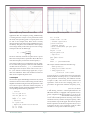
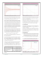
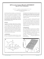
Connecting TCAD To Tapeout
A Journal for Circuit Simulation and SPICE Modeling Engineers
Fast and Accurate Simulation of the Steady-State of Voltage
Controlled Oscillators with SmartSpice-RF
1. Abstract
fundamental frequency, and an open circuit at all other
frequencies. This component must be inserted in the
circuit to compute the frequency and oscillation level at
insertion point.
A novel simulation method of the steady-state of oscillators,
based on Harmonic Balance (HB), is presented. A comparison with regular transient simulations demonstrates its advantages on a feedback voltage-controlled oscillator (VCO).
First, SmartSpice RF uses an initialization procedure to
find the probe voltage corresponding to the probe admittance minimum at the oscillation frequency estimated
by the user. Then it operates an optimization procedure
to compute the oscillation frequency and magnitude of
the probe. This stage ends when the current across the
probe is considered as null (the probe is then like disconnected) or when the accuracy on oscillation frequency is
reached. At this frequency, the circuit must be an oscillator.
The method requires a good starting point for the oscillation frequency to have good convergence properties. If the
user doesn’t know accurately enough the expected oscillation frequency, a linear AC simulation, a S-parameter simulation can be run to determine a satisfying initial guess.
2. Introduction
Oscillators are the key components of many radio frequency (RF) circuits. Simulating their steady-state and extracting their characteristics (oscillation frequency, power
spectra, phase noise...) has become one of the most critical
challenge in the design flow. Regular SPICE transient simulations suffer from severe drawbacks on these circuits.
First, simulation run times are often prohibitive to reach
the steady-state, particulary for high-Q circuits, which
are the major part of today’s RF applications. Second, it is
necessary to manually start the oscillator, which is not an
easy task and can lead to false steady-states. Third, phase
noise characteristics can not be extracted directly from
transient results. And sweeping a parameter (for example,
to study the oscillation frequency dependance of a VCO)
is very costful, since the simulation time is simply multiplied by the number of sweeping points.
Success and efficiency of analysis depends also on where
the probe is connected. Typically, it should be inserted in
parallel with the resonator or in parallel with the load.
Since the probe must have some effect on the oscillation,
it should not be placed after the buffer nor in the biasing
circuitry. SmartSpice-RF can handle 1-tone autonomous
circuits, as well as efficient parametric sweep, allowing
SmartSpice-RF propose a new method which remains
fast and accurate in all these situations where transient
simulation fails or shows poor performance. Based on
Harmonic Balance, the oscillator steady-state is computed
directly in the frequency-domain thanks to a two-stages
method. In the following, we first describe briefly the
method, then shows its application on a feedback VCO
and compares its performance to transient simulations.
Continued on page 2 ...
INSIDE
SET Accurate Compact Model for SET-MOSFET
Hybrid Circuit Simulation ......................................... 4
3. Basics of the Method
A Sophisticated Verilog-A Debugger.......................... 7
A two-stages approach [1] is used to compute the steadystate of autonomous circuits. It uses the concept of a
probe. A probe is a special-purpose voltage source which
behaves as a pure sinusoidal generator at the oscillation
Volume 14, Number 10, October 2004
October 2004
Calendar of Events.................................................... 10
Hints, Tips, and Solutions ......................................... 11
Page 1
The Simulation Standard
Figure 1. Output voltage waveforms at node 3 and 4.
Figure 2. Power spectrum at output node.
applications like VCO frequency tuning. Additionnally,
a small-signal noise analysis can be performed around
the steady-state operating point to compute phase noise
(as well as total output noise). Phase noise is usually
characterized in terms of the single-sideband noise spectral density. The phase noise is defined as mean-square
noise voltage density to the mean-square carrier voltage,
and reports the ratio in decibels [2]:
L(Δω) = 10log
D1 4 3 DioN
D2 3 4 DioN
.model DioN D is=.1fA
; Tunable capacitance
.param Ctune=1nF
; Feedback network
.subckt FeedbackNet pIn pOut pGnd
; Resistors
RA pIn 1 15.8k
RB pOut pGnd 15.8k
; Capacitors
CA 1 pOut ’Ctune’
pOut pGnd ’Ctune’
.ends
v2n/(Δƒ)
v2sig
The most commonly used unit for phase noise is power
below the carrier per Hertz, expressed in dB, or dBc/Hz, at
some offset frequency Δω from the carrier frequency ω0.
XRes1 3 1 gnd FeedbackNet
One of the possible ways to model phase noise in oscillators is a noise mixing analysis. The noise at the sidebands
on either side of the carrier (ω0 ± ∆ω ) is obtained from
small-signal mixer analysis where noise sources (Δω +
kω0 ) mix with the oscillator large signals (kω0) to produce noise sidebands. These noise simulation results are
then used to compute the phase noise.
The analysis statement looks like the following:
.HOSCIL probe(3,1)
+ fund_osc=12.591kHz nharm=7
+ fund_osc_reltol=0.1
+ sweep Ctune 0.8n 1.2nF 0.05nF
A logical choice is to connect the probe in parallel with
the RC feedback network (probe(3,1)). The theoretical
center pulsation characterizing the feedback network
is equal to 1/(RC). Let R and C be the resistance and
capacitance values of the first sweeping point. It is a
good choice for the initial oscillation frequency (fund_
osc=12.591kHz).
4. Example
We consider a regular Wien-Bridge oscillator circuit, which
contains two basic sections: an RC tuning network and an
amplifier. In the RC tuning network, the capacitance value
Ctune can be swept to control the oscillator frequency. A
UA741 amplifier is used, containing 16 BJT transistors. The
corresponding SPICE netlist is given below:
The specified number of harmonics ((nharm=7) is chosen
so that aliasing, which is a common phenomenon to all
HB-based methods, is negligible. The required accuracy
on the computed oscillation frequency is set to 0.1 Hz
(fund_osc_reltol=0.1). The HOSCIL statement propose
a lot of other tunable parameters allowing a fine control
of both the accuracy and the convergence quality, which
are beyond the scope of this paper. The last line specifies
that the capacitance of the RC tuning network (Ctune) is
swept from 0.8 nF to 1.2 nF, with steps of 0.05 nF, which
will induce a sweep of the oscillator frequency.
; Sources
Vcc vcc gnd dc=15
Vee vee gnd dc=-15
; Op Amp
XAmp1 1 2 3 ua741
; Resistors
R1 2 gnd r=10k
; Amplitude stabilization network
R3 2 3 r=21k
R4 2 4 r=200k
The Simulation Standard
Page 2
October 2004
Figure 3. Transient output waveform at node 4.
Figure 4. Oscillation frequency tuning.
After a few seconds, the steady-state results are available. The figures 1 and 2 show examples of waveforms
and spectra obtained at the point Ctune = 1 nF.
quency domain. For parametric simulations with a high
number of sweeping points, the performance improvement is even more important.
With a regular transient simulation (TRAN statement),
the VCO must be started (for example using an initial
condition [3]) and the steady-state is only reached after
a lot of simulation time points, when all transients have
sufficiently vanished. It is completely prohibitive for circuits with a high-Q factor or for circuits containing elements like transmission lines which are better described
directly in the frequency domain by HOSCIL (whereas
TRAN uses costful convolution techniques).
Furthermore, HOSCIL analysis proposes an efficient
small-signal noise analysis around the oscillator steadystate, allowing the extraction of phase noise, which is a
crictical figure-of-merit of modern oscillator designs.
5. Conclusion
In this paper, the advantages of the new harmonic balance-based method (HOSCIL) for the simulation of
oscillators, included in SmartSpice-RF
SmartSpice-RF, have been demonstrated. It is definetly more reliable and much faster
than regular transient approaches for applications like
VCO frequency tuning, and it allows easy and accurate
phase noise extraction.
With HOSCIL analysis, each point in the parametric analysis
will use the result from a previous run as an initial guess.
The convergence of the subsequent points is then much
faster. The fundamental oscillation frequency can be easily
extracted for each run, through a .measure command.
6. References
.measure hop_sp fosc AMAX vdb(3)
[1]
Figure 4 shows the oscillation frequency as a function of
the control capacitance.
E.Ngoya, A. Suarez, R. Sommet, R. Quere, Steady State Analysis
of Free or Forced Oscillators by Harmonic Balance and Stability
Investigation of Periodic and Quasi-Periodic Regimes. Int. J. Microwave and Millimeter-Wave CAD, Vol. 5, No. 3, pp 210-233, 1995.
[2] T. H. Lee, The Design of CMOS Radio-Frequency Integrated Circuits. Cambridge University Press, 1998.
With TRAN analysis, the parametric analyis is equivalent to as many indepent runs as swept points. Besides,
the oscillation frequency has to be extracted carefully
with a subsequent measurement (when have we really
reached the true steady-state ?).
[3] K. S. Kundert, Steady-State Methods for Simulating Analog and
Microwave Circuits, Kluwer Academic Publishers, May 1990.
Table 1 gives a comparison of the CPU time between HOSCIL
and TRAN depending on the number of sweeping points.
The speedup is significant even for a single run since
HOSCIL computes directly the steady-state in the freNumber of Sweeping Points
TRAN CPU time (s)
HOSCIL CPU time (s)
Speedup (%)
1
5
10
20
3.09
6.12
9.15
12.18
1.7
2.4
3.1
3.8
45.0
60.8
66.1
68.8
Table 1. Performance comparison between TRAN and HOSCIL
analyses.
October 2004
Page 3
Figure 5. Relative phase noise plot at output node.
The Simulation Standard
SET Accurate Compact Model for SET-MOSFET
Hybrid Circuit Simulation
C. Le Royer*, G. Le Carval*, M. Sanquer**
* CEA-DRT-LETI - CEA/GRE, 17 rue des Martyrs, 38054 Grenoble Cedex 9, France
[email protected], [email protected]
** CEA-DRFMC, 17 rue des Martyrs, 38054 Grenoble Cedex 9, France
[email protected]
works [5][6] show that Single-Electron Transistors could
enable innovative functionalities if they are associated
with MOSFETs. However Monte-Carlo (MC) simulation
[8] is not adapted to the analysis and the optimization
of realistic logic circuits with a large number of devices
(MOSFETs and SETs).
The following article, by Le Royer, C., Le Carval, G., Sanquer, M.: SET Accurate Compact Model for SET-MOSFET
Hybrid Circuit Simulation. In: Wachutka, G., Schrag,
G. (eds.), Simulation of Semiconductor Processes and
Devices 2004. Wien - New York: Springer. 2004 (http://
www.springer.at/main/book.jsp?bookID=3-211-22468-8),
demonstrates the flexibility of SmartSpice used with its
module Verilog-A in the simulations of SET circuits and
hybrid SET-MOSFET circuits.
In this paper, we propose a compact physically based
SET model, describing SET characteristics accurately
over a wide range of temperature and voltages [4].
Our approach is simpler and more efficient than those
presented in the literature [9][10]. Our model has been
validated in static and dynamic regimes [4], at both device
and logic circuit levels, by comparison with the MC
simulator SIMON [8].
Abstract
Single-Electron Transistors (SETs) [1][2] are attractive
candidates for post-CMOS VLSI ICs. Accurate models
are also required in order to efficiently design SET
circuits and hybrid circuits. We have developed a new
physical compact model of SET [3][4], which enables the
accurate simulation of SET circuits and hybrid circuits in
a SPICE-like environment. We show advanced examples
of applications of our approach: simulations of elementary
circuits which functionalities have been experimentally
demonstrated in the literature [5][6].
2 SET Modeling
Our model is derived on the basis of the “orthodox”
theory of single charge tunnelling and the master equation method [1][2]. The number of elementary charges e
in the SET island (Figure 1.a) is supposed to be n = -1, 0
or +1. This model (detailed elsewhere [4]) is built on this
assumption and the periodicity of the current IDS(VGS):
the average IDS current (Figure 2.b) is determined as a
function of the VDS and VGS voltage, the temperature and
the offset charges, q0.
1 Introduction
SETs have attracted much attention because of their
low power consumption and small size [1][2][7]. Recent
a)
b)
Figure 1: a) Schematic representation of a Single-Electron Transistor. b) Example of current IDS calculated with our model. The blockade
regions (diamond shape) can be clearly distinguished.
The Simulation Standard
Page 4
October 2004
a)
b)
Figure 2: a) Example of relative error (%) between MC simulation and our model in the VDS -VGS diagram. In the central region the accuracy is better than 1.5%. b) Theoretical limits of validity of our model (which correspond to the MC results).
We have checked that, in the dynamic or static regime,
the difference between ourmodel and MC simulation
(Figure 2) is less that 1.5% for |VDS| ≤ 2e/CΣ (CΣ = C1 +C2
+ CG is the total capacitance of the central island), which
is two times the limit of the models proposed by Uchida
[9] or Mahapatra [10]). We have checked that thisresult
does not depend on the SET parameters (capacitances,
resistances) and isvalidated for a large range of temperature (kT / EC < 0.1).
3.2 Hybrid SET-MOSFET Circuits
We have also simulated the electrical behaviour of two
hybrid MOSFET-SET circuits: a SRAM cell [5] and a
“quantizer” [6] (Figure 5) proposed by Inokawa.
For most simulation parameters, we have considered the
values extracted by Inokawa from measurements. We
have used the following values: MOSFET: L = 14µm / W
= 12µm / Tox = 9.45nm - SET : CJ = 1.8aF / CG = 0.07aF / Rt
= 150kΩ / q0 = e/2 / Vgg = 1.04V[5].
3. Applications to Hybrid MOSFET-SET
Simulation
3.1 Ring Oscillator with SETs
The first logic gates that we have simulated with our
model (in SmarSpice with Verilog-A [11]) are ring oscillators composed of 2p+1 SET inverters [11] (Figure 3).
The voltages V1, V2 and V3 are the outputs of the 3 inverters. The supply voltages are +VD and -Vd. This circuit
generates oscillating signals like in the case of CMOS
inverters. Figure 4 shows the voltages of the outputs of
the three inverters as a function of time, obtained by a
SmartSpice simulation [11]. This proves that our model
allows to simulate this oscillating behaviour.
Figure 3: Ring oscillator with 3 SET inverters.
Figure 4: Simulation of the ring oscillator behaviour. When the supply voltage Vd is increased
October 2004
Page 5
The Simulation Standard
Figure 5: Schematic circuits proposed by Inokawa a) SRAM cell [5] (the multiple-value memory effect is due to the V-I hysteresis). b) “quantizer”
[6] (the signal Vin is sampled with respect to the frequency defined by the “Clock” MOSFET along the stability points a, b, …, f).
Figure 6: a) Current characteristic I(V) of the sub-circuit of the SRAM cell calculated by hybrid SPICE simulation. b) Multivalued hysteresis
effect of the SRAM cell simulated by our model.
[5] H. Inokawa, A. Fujiwara, and Y. Takahashi, DRC Conference Digest, pp. 129-130, 2001.
The simulated results (Figure 6 and Figure 7) show a
very good agreement with these experimental measurements [5][6].
[6] H. Inokawa, A. Fujiwara, and Y. Takahashi, IEDM, pp. 147-150, 2001.
[7] A. N. Korotkov et al., Appl. Phys. Lett., Vol. 68, N°14, pp. 19541956, 1996.
4 Conclusions
[8] C. Wasshuber, H. Kosina, S. Selberherr, Trans. Computer-Aided
Design of Integrated Circuits and Systems, Vol. 44, pp. 937-944,
Aug. 1997.
In this paper we propose a new compact model for
SET dedicated to SPICE simulation for SET circuits and
hybrid MOSFET-SET circuits. After showing the performances of our model, we apply it to the simulation of
SET Logic gates and hybrid MOSFET-SET circuits. We
demonstrate the accuracy of our model by the good
comparisons between the SPICE simulations and the
experimental measurements of these circuits [5][6].
[9] K. Uchida et al., Jpn. J. Appl. Phys., Part. 1, Vol. 39, N° 4, pp. 23212324, 30 Apr. 2000.
[10] S. Mahapatra et al., IEEE Electron Device Lett., Vol. 23, N° 6, pp
366–368, Jun. 2002.
[11] SmartSpice User’s manual Volume 2, Silvaco Data Systems, Santa
Clara, 2002.
Acknowledgment
The authors would like to acknowledge Silvaco’s contribution which greatly facilitated implementation of these
models within SmartSpice and Verilog-A.
References
[1]
H. Grabert and M. Devoret., «Single Charge Tunneling», Series B:
Physics Vol. 294, NATO ASI Series, Plenum Press, 1992.
[2] K. K. Likharev, Proc. of the IEEE, Vol. 87, Issue 4, pp.606- 632,
Apr. 1999.
[3] C. Le Royer et al., Proc of ESSDERC, Florence (Italy), pp. 403406, 24-26 Sept. 2002.
Figure 7: Simulation of the quantizer operation. The output
voltage Vout (with a staircase shape with respect to the stability
points) corresponds to the sampling of the triangular voltage Vin.
[4] C. Le Royer, PhD Thesis, Joseph Fourier University, Grenoble
(France), 17 Oct. 2003.
The Simulation Standard
Page 6
October 2004
A Sophisticated Verilog-A Debugger
During the elaboration of a Verilog-A model, debugging
a module can be very useful for detecting non-physical behavior or fine-tuning the model. The SILVACO
Verilog-A debugger has been designed to meet these
needs. It is available since version 2.6.0.R of SmartSpice
and works along with SILVACO C-Interpreter. It allows
iteration-per-iteration Verilog-A modules debugging.
The debugger is tracing all the Verilog-A instantiations
of the design, either instances of the SmartSpice netlist
or in other Verilog-A modules.
The BSIM4 Verilog-A model (bsim4.va) and the adder
design (adder.in) used as an example are freely available
on SILVACO website.
It can be enabled by setting in the input deck:
.OPTIONS va_mode=debug
The debugger appears when the simulation of this input deck is launched. The simulation stops at the first Figure 1. Debugger window layout.
instruction (a breakpoint at the first instruction is always
set by default). In the case of BSIM4 model, the first
insertion in the Verilog-A code using “insert/remove
instruction encountered is the initial_step event in the
breakpoint” button
. In the first method, a breakanalog block. The layout of the main window at startup
point condition can be set in the condition field. This
is shown in Figure 1.
condition can be of several kinds: it can include logical,
relational, bitwise, shift and arithmetical operators as
The Verilog-A source code is displayed in an editor winwell as mathematical and simulation-related functions,
dow. Syntax highlighting is available and its colors are
shown in Table 1.
fully customizable. Line numbers can be displayed by
checking the “Show line number” box in the Properties
dialog window (Edit > Properties...).
$realtime function can be of a great help for debugging
a model on a given time range. Supposing now that the
Bulk-Drain diode current value of a BSIM4 device has
to be checked for a time > 190 ns. A breakpoint is set
in “View breakpoints…” window at line 2878 (the end
of the bulk diodes calculations). The condition for this
breakpoint entered in next figure stops the simulation
during a transient analysis if time > 190 ns. The other
breakpoints are removed using ‘Delete’ button in the
same window (Figure 4).
The console window is at the bottom of the main window. The error messages are printed in this area and the
user can enter commands manually.
In this example (Figure 2. The console window), a breakpoint has been set at line 2699 (the end of the initial_step
block) and the simulation has been started with the cont
command. The edit window has now the aspect shown
in Figure 3.
I. Tracing Code in the Source Code Window
Verilog-A code in a module can be debugged step-bystep or by using breakpoints. Breakpoints can be set by
opening the “View breakpoints...” window or by a direct
Figure 2. The console window.
October 2004
Figure 3. Editing window.
Page 7
The Simulation Standard
The local variable panel shows all the variables, parameters and branch quantities values in the current context
(initial block, analog block or user-defined function).
These values are updated at each step. The panel next
to it shows the global variables related to current simulation. The running analysis as well as its parameters,
the SmartSpice engine iteration counter and the circuit
temperature are given.
Figure 4. Add a condition to a breakpoint.
By using “continue” button
, the simulation continues
and the debugger stops when time has reached 190 ns.
The current analysis and the current step (time in the
case of a transient analysis) are printed at the bottom
panel of the main window:
Figure 5. The bottom panel.
DC, AC, TRANS or NOISE can be displayed at this location according to the analysis run. The simulation step
can be the sweep value for DC analysis, the time for transient or the frequency for AC and NOISE. Cursor location
information in the source code window is also given.
“step into” and “step over” buttons
on the upper toolbar can be used to trace into or over the user-defined functions. Setting a breakpoint on a given function can be done
directly in the “View breakpoint...” window by inserting
the function name with “In function” box checked.
II. The Variable Watch Display
Once the debugger has reached the desired breakpoint, the
value of ‘cbd’ (Bulk-Drain diode current) can be checked.
Moving mouse cursor over the variable in the source code
window prints its value at current SmartSpice engine
iteration and current location in the module:
Figure 8. The global variables panel.
A third way to display ‘cbd’ value is to use the ‘watch’
panel next to the global variables panel. In this window,
only the variables asked by the user are displayed. To do
so, the name of the variable must be entered in the watch
dialog box
(Figure 9. The Add Watch dialog window).
Entering for example ‘cbd’ variable in the Add Watch
window has the effect of adding the variable to the current list of variables in the watch panel (see Figure 10.
The watch panel).
Figure 6. Variable value display in edit window.
Another way to display the ‘cbd’ variable is to look for
this variable in the local variable panel:
Figure 7. The local variables panel.
Figure 9. The Add Watch dialog window.
Function name
Description
analysis()
Analysis type. arguments must be “DC”, “AC”, “NOISE” or “TRAN”
initial_step()
Initial iteration. arguments must be “DC”, “AC”, “NOISE” or “TRAN”
final_step()
Final iteration. arguments must be “DC”, “AC”, “NOISE” or “TRAN”
$realtime
Current simulation time in transient analysis
$temperature
Current circuit temperature
Table 1.
The Simulation Standard
Page 8
October 2004
The level [0] is the SmartSpice netlist launched with the
simulator. The other stack levels can be a module instantiation within another Verilog-A module or a user-defined function. By double-clicking on a level of the stack,
the associated module is opened in the editor window
and the user can see where the next object in the stack is
instantiated. The last level of the call stack indicates the
current debugging location in the object at the bottom of
the hierarchy. In the case of the PLL example, the objects
related to the stack are:
Figure 10. The watch panel.
By using this latter method, the value of cbd can be easily monitored during the simulation. The values of the
asked variables in the watch panel are re-evaluated at
each debugger step.
III. The Call Stack Display
The call stack window displays the debugging location
inside the instance hierarchy. The following example is
a PLL Verilog-A module instantiated in the SmartSpice
netlist. This module is itself composed of other Verilog-A
modules (generator, phase detector, low-pass filter and
VCO). The hierarchy of the modules is:
Figure 12. An example of the hierarchy structure of the call stack
Module pll
Module pd
(phase detector)
Conclusion
Using a debugger can be of a great help when prototyping a model or when debugging a circuit design
which includes Verilog-A modules. Its great readability and ease of use allow the user to quickly fi nd
physical inconsistency in the model equations or in
the circuit design. The call stack window helps the
user to navigate easily through the design hierarchy.
Module vco
(Voltage Control
Oscillator)
Module capacitor
Module resistor
}
Low-pass
filter
Next figure shows the call stack content:
Figure 11. The call stack display.
Each level of the stack is of the following kind:
[level] instance_name(module_name), line_
number file_name
October 2004
Page 9
The Simulation Standard
Calendar of Events
October
1
2
3
4 IEEE SOI Conf. - Charleston, SC
FSA Modeling WS - Santa Clara, CA
5 IEEE SOI Conf. - Charleston, SC
FSA Modeling WS - Santa Clara, CA
6 IEEE SOI Conf. - Charleston, SC
FSA Suppliers Expo - San Jose, CA
7 IEEE SOI Conf. - Charleston, SC
8
9
10
11
12
13
14
15
16
17
18
19
20
21
22
23
24 IEEE Compound Symposium Monterey, CA
25 IEEE Compound Symposium Monterey, CA
26 IEEE Compound Symposium Monterey, CA
27 IEEE Compound Symposium Monterey, CA
28
29
30
November
1
2
3
4
5
6
7
8
9
10
11
12
13
14
15
16
17
18
19
20
21
22
23
24
25
26
27
28
29
30
31
Bulletin Board
FSA Model Checklist
As chairman of the FSA Model
Checklist working group (within the
FSA MS/RF Foundry committee),
Silvaco is attempting to duplicate
the success of the FSA PDK Checklist
with a common document that all
foundries would release with their
SPICE models. The objective of this
group is to develop a SPICE Model
Checklist with recommended circuit
measurements, and reports/graphs,
delivered with each foundry model,
to quantify and improve quality of
extracted foundry digital, analog,
and RF models. The group has
representatives from most of the
foundries who support mixed-signal
and RF process, as well as leading
MS/RF fabless companies. To find
out more about this group, e-mail
[email protected].
If you would like more information or to register for one of our our workshops, please check our web site at http://www.silvaco.com
The Simulation Standard, circulation 18,000 Vol. 14, No. 4, April 2004 is copyrighted by Silvaco International. If you, or someone you know wants a subscription to
this free publication, please call (408) 567-1000 (USA), (44) (1483) 401-800 (UK), (81)(45) 820-3000 (Japan), or your nearest Silvaco distributor.
Simulation Standard, TCAD Driven CAD, Virtual Wafer Fab, Analog Alliance, Legacy, ATHENA, ATLAS, MERCURY, VICTORY, VYPER, ANALOG EXPRESS,
RESILIENCE, DISCOVERY, CELEBRITY, Manufacturing Tools, Automation Tools, Interactive Tools, TonyPlot, TonyPlot3D, DeckBuild, DevEdit, DevEdit3D,
Interpreter, ATHENA Interpreter, ATLAS Interpreter, Circuit Optimizer, MaskViews, PSTATS, SSuprem3, SSuprem4, Elite, Optolith, Flash, Silicides, MC Depo/
Etch, MC Implant, S-Pisces, Blaze/Blaze3D, Device3D, TFT2D/3D, Ferro, SiGe, SiC, Laser, VCSELS, Quantum2D/3D, Luminous2D/3D, Giga2D/3D,
MixedMode2D/3D, FastBlaze, FastLargeSignal, FastMixedMode, FastGiga, FastNoise, Mocasim, Spirit, Beacon, Frontier, Clarity, Zenith, Vision, Radiant,
TwinSim, , UTMOST, UTMOST II, UTMOST III, UTMOST IV, PROMOST, SPAYN, UTMOST IV Measure, UTMOST IV Fit, UTMOST IV Spice Modeling,
SmartStats, SDDL, SmartSpice, FastSpice, Twister, Blast, MixSim, SmartLib, TestChip, Promost-Rel, RelStats, RelLib, Harm, Ranger, Ranger3D Nomad, QUEST,
EXACT, CLEVER, STELLAR, HIPEX-net, HIPEX-r, HIPEX-c, HIPEX-rc, HIPEX-crc, EM, Power, IR, SI, Timing, SN, Clock, Scholar, Expert, Savage, Scout, Dragon,
Maverick, Guardian, Envoy, LISA, ExpertViews and SFLM are trademarks of Silvaco International.
The Simulation Standard
Page 10
October 2004
Hints, Tips and Solutions
Colin Shaw, Applications and Support Engineer
Noise Simulations
Then yes the noise level for all 3 cases is the same but
this is a special case and if AF /= 1 then you get different
noise levels for the 3 cases A, B & C. In this particular
case the customer had a model card that contained the
parameter AF=1.72. Under these circumstances a difference of I 0.72 which is what was seen in the simulation.
Introduction:
A customer had 3 devices with identical current and
voltage applied.
A.
W/L = 10um/2um M=4
If I delete nlev=0 in the model file and substitute it with
“noimod=2” then, why are the thermal and flicker (1/F)
noises of all three cases not identical?
B. W/L = 40um/2um M=1
C. W/L = 10um/2um 4 devices in parallel
1.
If the MOS model file has the parameters: noia, noib,
noic, Af, Kf and nlev=0 will SmartSpice ignore the
BSIM III noise parameters (noia, noib and noic) and
simply use AK and KF?
Large Rawfile Handling in SmartView
There are various ways to calculate noise if the
model card includes the key word “nlev” then parameters Af & Kf are used. If this key word does not
appear in the model card then the parameters noia,
noib and noic are used.
2.
If smartspice does ignore noia, noib, noic when nlev
is set to nlev=0, then, why do these three cases I
have in the netlist not have the same identical
noise?
(flickernoise)2 =
KF. ids AF
KF. ids AF
NLEV=1
Cox. Leff. Weff. f
(flickernoise)2 =
Files greater than 2Gbyte must be on a local disk of
the PC (ie C: or D: not a network drive) otherwise
SmartView cannot read beyond the 2Gbyte limit.
This is a OS restriction.
2.
The incremental loading must be enabled. That is
SmartView will only load data from the rawfile as
it is required. This will limit th memory usage of
SmartView .
3.
In 32 bit applications (all current PC apps) have a
2GByte memory limit. No application can use more
than 2Gbyte of memory. this is a hard limit, only a
64bit OS can get round this problem.
4.
No 32bit application can control more than 2Gbyte
of system memory. Once the total amount of data
loaded reaches 2Gbyte, SmartView will stop. The
64 bit version on Solaris and Linux will work beyond this point.
NLEV=0
Cox. (Leff)2. f
(flickernoise)2 =
1.
KF. gm AF NLEV=2 or greater
Cox. Leff. Weff. fAF
If IDS is the current feed to each case (A,B,C) then
For A.
ids= IDS / 4
For each device
B.
ids= IDS
“
“
C.
ids= IDS/4
“
“
Call for Questions
If you have hints, tips, solutions or questions to contribute,
please contact our Applications and Support Department
Phone: (408) 567-1000
Fax: (408) 496-6080
e-mail: [email protected]
If AF=1 then
4 . ( IDS ) = IDS =
AF
( 4 )
October 2004
Hints, Tips and Solutions Archive
4 . ( IDS )
AF
Check our our Web Page to see more details of this example
plus an archive of previous Hints, Tips, and Solutions
Case A, B, C
www.silvaco.com
( 4 )
Page 11
The Simulation Standard
20 Years and Growing
Financially Rock-Solid
Fiercely Independent
Analog/MS EDA Design Leader
Contacts:
Silvaco Japan
[email protected]
Silvaco Korea
[email protected]
USA Headquarters:
Silvaco Taiwan
[email protected]
Silvaco International
4701 Patrick Henry Drive, Bldg. 2
Santa Clara, CA 95054 USA
Silvaco Singapore
[email protected]
Silvaco UK
[email protected]
Phone: 408-567-1000
Fax: 408-496-6080
Silvaco France
[email protected]
[email protected]
www.silvaco.com
Silvaco Germany
[email protected]
Products Licensed through Silvaco or e*ECAD
The Simulation Standard
Page 12
October 2004