1
COMPACTPCI-812
PERIPHERAL BOARD
USER’S MANUAL
The information in this document has been carefully checked and is believed to be entirely reliable. However, no
responsibility is assumed for inaccuracies. Furthermore, Cyclone Microsystems, Inc. reserves the right to make
changes to any products herein to improve reliability, function, or design. Cyclone Microsystems, Inc. neither
assumes any liability arising out of the application or use of any product or circuit described herein, nor does it
convey any license under its right or the rights of others.
Revision 1.0, August 2000
Cyclone P/N 800-0812
Copyright 2000 by Cyclone Microsystems, Inc.
CONTENTS
CHAPTER 1
GENERAL INTRODUCTION
1.1
INTRODUCTION.............................................................................................................................. 1-1
1.2
FEATURES ...................................................................................................................................... 1-2
1.3
OVERVIEW ...................................................................................................................................... 1-3
1.4
SPECIFICATIONS............................................................................................................................ 1-3
1.5
ENVIRONMENTAL...........................................................................................................................1-4
1.6
PHYSICAL ENVIRONMENT ............................................................................................................ 1-5
1.7
REFERENCE MANUALS .................................................................................................................1-6
CHAPTER 2
MPC8240 PROCESSOR
2.1
MPC8240 PROCESSOR.................................................................................................................. 2-1
2.2
BYTE ORDERING............................................................................................................................ 2-1
2.3
RESET VECTOR.............................................................................................................................. 2-1
2.4
POWERPC MPC603E CORE CACHE, BUFFERS, ARRAYS......................................................... 2-1
2.5
MEMORY MAP................................................................................................................................. 2-2
2.6
INTERRUPTS................................................................................................................................... 2-3
2.6.1 MPC8240 Interrupt Registers .............................................................................................. 2-3
2.6.2 Error Handling and Exceptions............................................................................................ 2-4
CHAPTER 3
HARDWARE
3.1
SDRAM............................................................................................................................................. 3-1
3.2
CONTROL MEMORY, T1XC & SUNI-PDH REGISTERS ................................................................ 3-1
3.3
FLASH ROM.....................................................................................................................................3-1
3.4
CONSOLE SERIAL PORT ............................................................................................................... 3-1
3.5
COUNTER/TIMERS ......................................................................................................................... 3-2
3.6
LEDS ................................................................................................................................................ 3-2
3.7
PCI INTERFACE .............................................................................................................................. 3-3
3.7.1 Primary PCI Arbitration........................................................................................................ 3-3
3.7.2 Secondary PCI Arbitration................................................................................................... 3-3
3.8
DMA CHANNELS ............................................................................................................................. 3-3
3.9
MESSAGE UNIT .............................................................................................................................. 3-4
3.10 JTAG/COP SUPPORT.....................................................................................................................3-4
3.11 GEOGRAPHIC ADDRESSING ........................................................................................................ 3-5
3.12 I2C BUS............................................................................................................................................3-6
3.12.1 Temperature Sensors.......................................................................................................... 3-6
3.13 HOT SWAP ...................................................................................................................................... 3-6
3.13.1 Hot Swap Extraction Process .............................................................................................. 3-7
3.13.2 Hot Swap Insertion Process ................................................................................................3-7
3.14 DS1 CONNECTOR .......................................................................................................................... 3-7
3.15 BOARD ID REGISTER.....................................................................................................................3-7
CPCI-812 User’s Manual
Revision 1.0, August 2000
i
CONTENTS
CHAPTER 4
ATM PROGRAMMING INFORMATION
4.1
INTRODUCTION.............................................................................................................................. 4-1
4.2
DEVICE REGISTRES ...................................................................................................................... 4-2
4.2.1 ATM-SAR Mode Registers ................................................................................................. 4-2
4.2.2 SUNI-PDH REGISTERS ..................................................................................................... 4-3
4.2.3 T1XC Registers................................................................................................................... 4-4
4.3
SOFTWARE RESET ........................................................................................................................4-6
4.3.1 ATM-SARs Software Reset ................................................................................................. 4-6
4.3.2 SUNI-PDHs Software Reset................................................................................................4-6
4.4
LOOPBACK.....................................................................................................................................4-6
4.5
CLOCKING OPTIONS...................................................................................................................... 4-6
CHAPTER 5
pSOS SOFTWARE DEVELOPMENT
5.1
INTRODUCTION.............................................................................................................................. 5-1
5.2
EMBEDDED UTILITIES MEMORY BLOCK ..................................................................................... 5-1
5.3
ENDIAN CONSIDERATIONS........................................................................................................... 5-2
5.4
PCI CONFIGURATION .................................................................................................................... 5-2
5.4.1 Downstream (Inbound) CompactPCI Transactions ............................................................. 5-3
5.4.2 Upstream (Outbound) CompactPCI Transactions............................................................... 5-3
5.4.3 PLX PCI9080 Configuration ................................................................................................5-3
5.4.4 Changing PCI Configuration................................................................................................5-4
5.4.5 pSOS PCI Device Driver Interface ......................................................................................5-4
5.5
EPIC INTERRUPT PROGRAMMING............................................................................................... 5-5
5.5.1 Connecting and Disconnecting Interrupt Handlers in pSOS................................................ 5-6
5.6
LM75 TEMPERATURE SENSORS.................................................................................................. 5-7
APPENDIX A
PCI LOCAL BUS SIGNALS
A.1
ii
INTRODUCTION............................................................................................................................. A-1
CPCI-812 User’s Manual
Revision 1.0, August 2000
CONTENTS
LIST OF FIGURES
Figure 1-1.
CPCI-812 Block Diagram ....................................................................................................1-1
Figure 1-2.
Physical Configuration......................................................................................................... 1-5
Figure 2-1.
CPCI-812 Memory Map.......................................................................................................2-2
Figure 3-1.
LED Register Bitmap, FF20 0000H..................................................................................... 3-3
Figure 3-2.
MPC8240 Processor DMA Controller.................................................................................. 3-4
Figure 3-3.
JTAG/COP Header Orientation........................................................................................... 3-5
Figure 3-4.
Geographic Addressing Register, FF60 0000H...................................................................3-6
Figure 3-5.
Board Identification Registers, FF70 0000h ........................................................................ 3-7
Figure 5-1.
Embedded Utilities Memory Block....................................................................................... 5-2
Figure 5-2.
PCI_LOC Structure Definition.............................................................................................. 5-5
PCI-731 User’s Manual
Revision 1.0, September 2001
iii
CONTENTS
LIST OF TABLES
Table
Table
Table
Table
Table
Table
Table
Table
Table
Table
Table
Table
Table
Table
Table
iv
1-1.
1-2.
2-1.
2-2.
3-1.
3-2.
3-3.
3-4.
3-5.
4-1.
4-2.
4-3.
4-4.
5-1.
5-2.
CPCI-812 Power Requirements .......................................................................................... 1-4
Environmental Specifications .............................................................................................. 1-4
Serial Interrupt Assignment ................................................................................................. 2-3
Error Priorities...................................................................................................................... 2-4
Console Port Connector ...................................................................................................... 3-1
UART Register Addresses .................................................................................................. 3-2
JTAG/COP PIN ASSIGNMENT........................................................................................... 3-5
I2C Device Addresses......................................................................................................... 3-6
DS1 Connector ................................................................................................................... 3-7
Secondary Address Map for ATM-SAR Registers .............................................................. 4-1
ATM-SAR General Mode Register ......................................................................................4-2
SUNI-PDH Non-Default Register Settings........................................................................... 4-3
T1XC Non-Default Register Settings...................................................................................4-5
PLX PCI9080 Base Address Registers on CPCI-812 ......................................................... 5-4
CPCI-812 Interrupt Vectors ................................................................................................. 5-6
CPCI-812 User’s Manual
Revision 1.0, August 2000
CHAPTER 1
GENERAL INTRODUCTION
1.1
INTRODUCTION
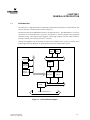
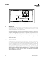
The CPCI-812 is a high-performance CompactPCI peripheral board featuring two ATM SARs for dual
DS1 line interface. A block diagram is shown in Figure 1-1.
The board is based on the MPC8240 PowerPC integrated processor. The MPC8240 has a processor
core based on the PowerPC603e low-power microprocessor, and also performs many peripheral
functions on chip. The peripheral logic integrates a PCI bridge, memory controller, DMA controller,
interrupt controller, I 2O controller, and an I 2C controller.
Software development tools for PowerPC processors are available from a variety of vendors, and a
Board Support Package (BSP) for the pSOS operating system is available from Cyclone.
DS1
ATM0
DS1
ATM1
Console
Serial Port
JTAG
I/F
2 Mbytes
Flash ROM
64
Mbytes
SDRAM
MPC8240
Processor
PCI-to-PCI
Bridge
PCI-to-SAR
Bridge
32-bit Secondary PCI Bus
64-bit CompactPCI Bus
Figure 1-1. CPCI-812 Block Diagram
CPCI-812 User’s Manual
Revision 1.0, August 2000
1-1
GENERAL INTRODUCTION
1.2
1-2
•
FEATURES
MPC 8240 Processor
•
21554 PCI-to-PCI Bridge
The 21554 is a “non-transparent” PCI-to-PCI bridge with a 64-bit
primary bus interface and a 64-bit secondary interface. A nontransparent bridge allows the local processor to configure and
control the local subsystem. The 21554 primary bus interfaces with
the 64-bit CompactPCI bus and the secondary bus interfaces with
the 32-bit PCI bus of the MPC8240.
•
SDRAM
64 MBytes of ECC SDRAM is standard on the CPCI-812.
The microprocessor is Motorola’s integrated MPC8240 PowerPC.
The device integrates a Motorola 32-bit superscalar PowerPC 603e
core, running at 250 MHz internally, and Peripheral Components
Interconnect (PCI). The core boasts a 16 Kbyte instruction cache, a
16 Kbyte data cache and floating-point support. Memory can be
accessed through the memory controller to the core processor or
from the PCI bus.
• CompactPCI Interface
The CPCI-812 meets the PICMG 2.0 Rev. 2.1 Specification for
system slot adapters. The PCI bus runs at 33MHz.
•
Flash ROM
2 Mbytes of in-circuit sector-programmable Flash ROM.
•
Console Serial Port
An RS-232 serial port is provided for a console terminal or
workstation connection. The serial port supports up to 115 Kbps
and uses a phone jack to DB25 cable supplied with the CPCI-812
board.
•
Hot Swap
The CPCI-812 is a Full Hot Swap board, compliant with PICMG
2.1.
•
Timers
Four 31-bit timers are available to generate interrupts.
•
DMA Controller
The MPC8240 supports 2 separate DMA channels for high
throughput data transfers between PCI bus agents and the local
SDRAM memory.
•
I 2O Messaging
The CPCI-812 supports the I2O specification for interprocessor
communication.
• Hardware Segmentation
Complete hardware segmentation of user packets to ATM cells,
including physical layer convergence and transmission over a
DS1(1.554Mbit/s twisted pair) line.
• Hardware Assembly
Complete hardware assembly of ATM cells received on a
DS1(1.554Mbit/s twisted pair) line into user packets.
• Memory Access
Direct memory access of packets stored in host memory for
segmentation and reassembly.
CPCI-812 User’s Manual
Revision 1.0, August 2000
GENERAL INTRODUCTION
1.3
OVERVIEW
The CPCI-812 is a 6U CompactPCI peripheral board with two ATM-DS1 interfaces, which uses three
VLSI circuits (ATM SAR, T1XC & SUNI-PDH). The ATM SAR performs hardware segmentation
of user packets into ATM cells and hardware reassembly of ATM cells into user packets. The SUNIPDH implements the mapping of ATM cells into the DS1 frame structure. The T1XC provides the DS1
line interface.
The CPCI-812 has two PCI buses, a primary and a secondary. The primary PCI bus is the CompactPCI
bus. The secondary PCI bus is a local bus that supports the MPC8240 and PLX PCI9080 bridge, which
interfaces the ATM SARs.
The CPCI-812 uses an Intel 21554 Embedded PCI-to-PCI Bridge to bridge between the primary
CompactPCI bus and the secondary local PCI bus. This device complies with the PCI Local Bus Specification, revision 2.1. It provides concurrent bus operation, allows buffering for both read and write
transactions and provides support for Hot Swap operation.
The primary PCI interface is 64-bit data but will operate correctly when the CPCI-812 is plugged into a
32-bit CompactPCI slot. Although the secondary PCI bus of the 21554 is 64-bit data, the local bus of
the CPCI-812 is 32-bit, the MPC8240 and PCI9080 are 32-bit PCI devices. The data path to memory of
the CPCI-812 is 64-bit. The memory controller resides on the MPC8240.
The Flash ROM on the CPCI-812 can be reprogrammed by software through a JTAG/COP interface.
Utilities to perform this programming are available from software development tool vendors.
Additional information on the JTAG/COP interface can be found in section 3.10.
1.4
SPECIFICATIONS
Physical Characteristics
Power Requirements
CPCI-812 is a single slot, double high CompactPCI peripheral card.
Height:
9.187” (233.35mm) Double Eurocard (6U)
Depth:
6.299” (160mm)
Width:
.8” (20.32mm)
The CPCI-812 requires +5V, +12V and +3.3V from the CompactPCI
backplane J1 connector.
The following table represents the power consumption of the CPCI-812.
CPCI-812 User’s Manual
Revision 1.0, August 2000
1-3
GENERAL INTRODUCTION
Table 1-1. CPCI-812 Power Requirements
1.5
Voltage
Current Typical
Current Maximum
+3.3V
2.411 Amps
3.465 Amps
+5V
2.197 Amps
3.144 Amps
+12V
0.002 Amps
0.003 Amps
-12V
0 Amps
0 Amps
ENVIRONMENTAL
The CPCI-812 should be operated in a CompactPCI card cage with good air flow. The board can be
operated at ambient air temperature of 0-55 degrees Celsius, as measured at the board.
Table 1-2. Environmental Specifications
Operating Temperatures
Relative Humidity
(non-condensing)
Storage Temperatures
1-4
0 to 55 Degrees Celsius
0-95%
-55 to 125 Degrees Celsius
CPCI-812 User’s Manual
Revision 1.0, August 2000
GENERAL INTRODUCTION
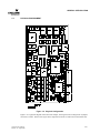
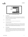
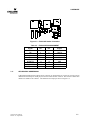
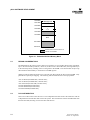
1.6
PHYSICAL ENVIRONMENT
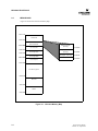
Figure 1-2. Physical Configuration
Figure 1-2 is a physical diagram of the CPCI-812 Adapter, showing the location designators of jumpers,
connectors, and ICs. Refer to this figure when component locations are referenced in the manual text.
CPCI-812 User’s Manual
Revision 1.0, August 2000
1-5
GENERAL INTRODUCTION
1.7
REFERENCE MANUALS
MPC8240 Integrated Processor User’s Manual
Order Number MPC8240UM/D Rev. 0
Motorola Literature Distribution
P.O. Box 5405
Denver, CO 80217
(800) 441-2447
LM75 Digital Temperature Sensor and Thermal
Watchdog
National Semiconductor Corporation
1111 West Bardin Road
Arlington, TX 76017
(800) 272-9959
PowerPC Microprocessor Family:
The Programming Environments for
32-bit Microprocessors, Rev. 1
Order Number MPCFPE32B/AD
Motorola Literature Distribution
P.O. Box 5405
Denver, CO 80217
(800) 441-2447
CompactPCISpecification
PCI Industrial Computers Manufacturing Group
301 Edgewater Place, Suite 220
Wakefield, MA 01880
(617) 224-1100
(617) 224-1239 Fax
TL16C550C UART
Texas Instruments
http://www.ti.com/sc/docs/general/dsmenu.htm
PCI-9080
PLX Technology, Inc.
390 Potrero Avenue
Sunnyvale, CA 94086
(800) 759-3735
(408) 774-2169 Fax
http://www.plxtech.com
Local ATM SAR Chip User’s Manual
(uPD 98401)
NEC Electronics, Inc.
475 Ellis Street
P.O. Box 7241
Mountain View, CA 94039
PCI Local BIOS Specification, Revision 2.1
PCI Special Interest Group
2575 NE Kathryn Street #17
Hillsboro, OR 97214
(800) 433-5177 (U.S.)
(503) 693-6232 (International)
(503) 693-8344 (Fax)
I2 O Specification, Revision 1.0
I2 O Special Interest Group
(415) 750-8352
http://www.i2osig.org
CompactPCI Hot Swap Specification, PICMG
2.1, R1.0
PCI Industrial Computers Manufacturing Group
301 Edgewater Place, Suite 220
Wakefield, MA 01880
(617) 224-1100
(617) 224-1239 Fax
T1 Framer/Transceiver
(T1XC, PM4341A)
Saturn User Network Interface
(S/UNI-PDH, PM7345)
PMC-Sierra, Inc.
8501 Commerce Court
Burnaby, BC Canada V5A 4N3
(604) 668-7300
1-6
CPCI-812 User’s Manual
Revision 1.0, August 2000
CHAPTER 2
MPC8240 PROCESSOR
2.1
MPC8240 PROCESSOR
The MPC8240 contains a PowerPC 603e core processor. The core is configured to run at 250 MHz.
This RISC processor utilizes a superscalar architecture that can issue and retire as many as three instructions per clock. The core features independent 16 Kbyte, four-way set-associative, physically addressed
caches for instructions and data and on-chip instruction and data memory management units (MMUs).
2.2
BYTE ORDERING
The CPCI-812 is designed to run in big endian mode. The byte ordering determines how the core
accesses local memory and the PCI bus. Big endian stores the most significant byte in the lowest
address.
2.3
RESET VECTOR
The 8-bit wide Flash ROM is located in the address range FFE0 0000h through FFFF FFFFh. See
Figure 2-1, the CPCI-812 memory map. The MPC8240 reset vector is located at address FFF0 0100h.
This reset vector location, which contains a branch to the rest of the boot code, is essentially in the
middle of the ROM device. This positioning results in a break up of continuous memory space and
approximately 50% reduction in usable space for boot code. To better utilize this device, the CPCI-812
re-maps the reset vector to FFE0 0100h by inverting memory address 20 (A20) for the first two
processor accesses to memory. These accesses are an absolute jump instruction to the beginning of boot
code. After this jump, A20 functions normally. Utilizing this method, the majority of the 2 Mbyte
Flash ROM can be used.
2.4
POWERPC MPC603E CORE CACHE, BUFFERS, ARRAYS
The processor core provides independent on-chip, 16-Kbyte, four-way set-associative, physically
addressed caches for instructions and data, and on-chip instruction and data memory management units
(MMUs). The MMUs contain 64-entry, two-way set associative, data and instruction lookaside buffers
(TLB) that provide support for demand-paged virtual memory address translation and variable-sized
block translation. The processor also supports block address translation (BAT) arrays of four entries
each.
As an added feature to the MPC603e core, the MPC8240 can lock the contents of one to three ways in
the instruction and data cache (or the entire cache).
CPCI-812 User’s Manual
Revision 1.0, August 2000
2-1
MPC8240 PROCESSOR
2.5
MEMORY MAP
Figure 2-1 shows the CPCI-812 memory map.
FFFF FFFF
Flash ROM
FFE0 0000
On-board Devices
FF00 0000
Board ID Register
(read only)
PCI INT ACK
FEF0 0000
FF70 0000h
Geographic Address
PCI Config DATA
(read only)
FEE0 0000
PCI Config ADDR
LED Register (write only)
FEC0 0000
UART
PCI I/O Space
FF60 0000h
FF20 0000h
FF00 0000h
FE00 0000
PCI Memory Space
8000 0000
Reserved
4000 0000
DRAM
0000 0000
Figure 2-1. CPCI-812 Memory Map
2-2
CPCI-812 User’s Manual
Revision 1.0, August 2000
GENERAL INTRODUCTION
2.6
INTERRUPTS
The CPCI-812 interrupt scheme is based upon the MPC8240 processor’s embedded programmable
interrupt controller (EPIC). The EPIC unit is set to serial interrupt mode. Serial interrupt mode allows
for a maximum of 16 external interrupts. Table 2-1 shows the assignment of devices to serial interrupts
on the CPCI-812, all the interrupts are level sensitive.
The EPIC interface also contains several internal interrupt sources. These include the four global
timers, the two DMA channels, the I 2C bus, and from the Message Unit.
In addition to the EPIC interface, errors detected by the MPC8240 are reported to the processor core by
asserting an internal machine check signal Many of the errors detected in the MPC8240 cause
exceptions to be taken by the processor core. The error reporting is provided for three of the primary
interfaces, processor core interface, memory interface, and the PCI interface.
The ATM-SARs, T1XCs and SUNI_PDHs generate interrupts. The SUNI-PDHs and T1XCs interrupt
via the ATM-SARs. Thus there are only two interrupts required SAR1_INT and SAR2_INT. If the
SUNI_PDH or T1XC is the interrupt source, the ATM-SARs will interrupt the host and will have a bit
set in its status register, indicating that the SUNI-PDH or T1XC was the interrupt source.
Table 2-1. Serial Interrupt Assignment
2.6.1
INTERRUPT
INTERRUPT SOURCE
POLARITY
0
MIC_INTB
0
1
MIC_INTA
0
2
SAR1_INT
0
3
SAR2_INT
0
4
UART
1
5
Temperature (LM75s)
0
6
LSERR (PCI9080)
0
7
SINT A (21554)
0
8
MIC_INTD
0
9
MIC_INTC
0
10
Not Used
X
11
Not Used
X
12
Not Used
X
13
Not Used
X
14
Not Used
X
15
Not Used
X
MPC8240 Interrupt Registers
The MPC8240 processor has several different EPIC register maps to facilitate the handling of interrupts
which are briefly mentioned below. These registers occupy a 256Kbyte range of the embedded utilities
memory block (EUMB) and can be read and written by software. Please refer to the Motorola
MPC8240 User’s Manual for more details.
CPCI-812 User’s Manual
Revision 1.0, August 2000
2-3
MPC8240 PROCESSOR
2.6.2
Global EPIC Registers
Provides programming control for resetting, configuration and initialization of the external interrupts. Additionally, a vector register is
provided to be returned to the processor during an interrupt
acknowledge cycle for a spurious vector.
Global Timer Registers
Each of the four global timers have four individual configuration
registers. The registers are the Current Count register, the Base Count
register, the Vector/Priority register, and the Destination register.
Interrupt Source
Configuration
This group of registers are made up of the vector/priority and
destination registers for the serial and internal interrupt sources. This
includes the masking, polarity, and sense.
Processor-Related Registers
This group describes the processor-related EPIC registers. They are
made up of the Current Task Priority register, the Interrupt
Acknowledge register, and the End of Interrupt register.
Error Handling and Exceptions
Errors detected by the MPC8240 are reported to the processor core by asserting an internal machine
check signal (mcp#). The MPC8240 detects illegal transfer types from the processor, illegal Flash write
transactions, PCI address and data parity errors, accesses to memory addresses out of the range of
physical memory, memory parity errors, memory refresh overflow errors, ECC errors, PCI master-abort
cycles, and PCI received target-abort errors. Table 2-2 describes the relative priorities and recoverability of externally-generated errors and exceptions.
Table 2-2. Error Priorities
2-4
Priority
Exception
Cause
0
Hard reset
Power-on reset, CompactPCI chassis reset switch or
via JTAG controller
1
Machine check
Processor transaction error or Flash error
2
Machine check
PCI address parity error or PCI data parity error when
the CPCI-812 is acting as the PCI target
3
Machine check
Memory select error, memory refresh overflow, or
ECC error
4
Machine check
PCI address parity error or PCI data parity error when
the CPCI-812 is acting as the PCI master, PCI
master-abort, or received PCI target-abort
CPCI-812 User’s Manual
Revision 1.0, August 2000
CHAPTER 3
HARDWARE
3.1
SDRAM
The CPCI-812 is equipped with 64 Mbytes of ECC SDRAM mounted on the card. The memory is made
up of nine, 64Mbit (8M x 8) devices in an 8M by 72-bit configuration.
The memory controller unit (MCU) of the CPCI-812 supports SDRAM burst lengths of four. A burst
length of four enables seamless read/write bursting of long data streams as long as the MCU does not
cross the page boundary. Page boundaries are naturally aligned 2 Kbyte blocks. 72-bit SDRAM with
ECC running at 100MHz allows a maximum throughput of 800 Mbytes per second. The MCU keeps
four pages open simultaneously. Simultaneously open pages allow for greater performance for
sequential access, distributed across multiple internal bus transactions.
3.2
CONTROL MEMORY, T1XC & SUNI-PDH REGISTERS
The CPCI-812’s SRAM is control memory used exclusively by the ATM-SARs. The control memory
can be accessed via the ATM-SARs using an INDIRECT_ACCESS command.Parity generation and
checks are not performed on the control memory. As shown in the figure, the SUNI-PDH and T1XC
processor interfaces are also attached to the control memory bus. The SUNI-PDH and T1XC registers
are accessed via the ATM-SARs using an INDIRECT_ACCESS command.
3.3
FLASH ROM
The CPCI-812 provides 2 Mbytes of sector-programmable Flash ROM for non-volatile code storage.
The Flash ROM is located in local memory space at address FFE0 0000h through FFFF FFFFh. The
mapping ensures that, after a reset, the MPC8240 processor can execute the hard reset exception handler
located at FFF0 0100h.
3.4
CONSOLE SERIAL PORT
A single console serial port with an RS-232 line interface has been included on the CPCI-812. The port
is connected to a RJ-11 style phone jack on the adapter, and can be connected to a host system using the
included phone jack to DB-25 cable (Cyclone P/N 530-2002). The pinout of the console connector is as
shown in Table 3-1.
Table 3-1. Console Port Connector
Pin
Signal
1
CPCI-812 User’s Manual
Revision 1.0, August 2000
Description
Not Used
2
GND
Ground
3
TXD
Transmit Data
4
RXD
Receive Data
5
Not Used
6
Not Used
3-1
HARDWARE
K
Note
Pin 1 is the contact to the extreme left look in the console port opening, with the
tab notch facing down.
The serial port is based on a 16C550 UART clocked at 1.843 MHz. The device may be programmed to
use this clock with the internal baud rate counters. The serial port is capable of operating at speeds from
300 to 115200 BPS, and can be operated in interrupt-driven or polled mode. The 16C550 register set is
shown in Table 3-2. For a detailed description of the registers and device operation refer to the 16C550
databook.
Table 3-2. UART Register Addresses
3.5
Address
Read Register
Write Register
FF00 0000H
Receive Holding Register
Transmit Holding Register
FF00 0008H
Unused
Interrupt Enable Register
FF00 0010H
Interrupt Status Register
FIFO Control Register
FF00 0018H
Unused
Line Control Register
FF00 0020H
Unused
Modem Control Register
FF00 0028H
Line Status Register
Unused
FF00 0030H
Modem Status Register
Unused
FF00 0038H
Scratchpad Register
Scratchpad Register
COUNTER/TIMERS
The MPC8240 processor is equipped with four 31-bit on-chip counter/timers which count at 1/8 the
frequency of the SDRAM_CLK signal or 12.5MHz. Users should refer to the Processor User’s Manual
for the functionality and programming of the counters. The timers can be individually programmed to
generate interrupts to the processor when they count down to zero. Two of the timers, timer2 and
timer3, can be set up to automatically start periodic DMA operations for DMA channels 0 and 1,
respectively, without using the processor interrupt mechanism.
3.6
LEDS
The CPCI-812 has six green LEDs and one blue LED. The four green LEDs labeled IOP, ACT, STAT0,
and STAT1 are software driven and are controlled by a write-only register which is located at address
FF20 0000H. The LED Register bitmap is shown in Figure 3-1. Two green LEDs labelled LINK0 and
LINK1 are under ATM hardware control and indicate a valid DS1 link once the SUNI-PDH devices
have been initialized by software.
The blue LED is used for Hot Swap operations. Refer to section 3.14.1 for additional information.
3-2
CPCI-812 User’s Manual
Revision 1.0, August 2000
HARDWARE
Activity
Stat0
Stat1
IOP
(write only)
(1) LED on
(0) LED off
7
6
5
4
3
2
1
0
Figure 3-1. LED Register Bitmap, FF20 0000H
3.7
PCI INTERFACE
The CPCI-812 contains a primary 64-bit PCI bus and a secondary 32-bit PCI bus. Both buses are
clocked at 33 MHz. The primary PCI bus interfaces the 64-bit CompactPCI bus to the 21554 PCI-toPCI bridge. The secondary side of the 21554 interfaces a 32-bit PCI bus to the MPC8240 and the
PCI9080 bridge, which interfaces the two ATM SARs.
3.7.1
Primary PCI Arbitration
The primary PCI bus arbitration is provided by host of the CompactPCI system.
3.7.2
Secondary PCI Arbitration
Secondary bus arbitration logic between the MPC8240 processor, the 21554 bridge and the PCI9080
bridge, is contained within the MPC8240. The bus arbitration unit allows fairness as well as a priority
mechanism. A two-level round-robin scheme is used, in which each device can be programmed within
a pool of high- or low-priority arbitration. One member of the low-priority pool is promoted to the highpriority pool. As soon as it is granted the bus it returns to the low-priority pool.
3.8
DMA CHANNELS
The MPC8240 processor features two DMA channels. Data movement occurs on the PCI and/or
memory bus. Each channel has a 64-byte queue to facilitate the gathering and sending of data. Both the
local processor and PCI masters can initiate a DMA transfer. Some of the features of the MPC8240
DMA unit include: misaligned transfer capability, scatter gather DMA chaining and direct DMA
modes, and interrupt on completed segment, chain, and error. Figure 3-2 provides a block diagram of
the MPC8240 DMA unit.
CPCI-812 User’s Manual
Revision 1.0, August 2000
3-3
HARDWARE
To memory interface
DMA 1
DMA 0
FIFO
FIFO
Interface Logic
PCI Interface Unit
PCI Bus
Figure 3-2. MPC8240 Processor DMA Controller
3.9
MESSAGE UNIT
The MPC8240 provides a message unit (MU) to facilitate communications between the host processor
and peripheral processors. The MPC8240’s MU can operate with generic messages and doorbell
registers, and also implements an I 2O compliant interface.
The Intelligent Input Output (I 2O) specification allows architecture-independent I/O subsystems to
communicate with an OS through an abstraction layer. The specification is centered around a messagepassing scheme. An I2 O-compliant peripheral (IOP) is comprised of memory, processor, and input/
output devices. The IOP dedicates a certain space in its local memory to hold inbound (from the remote
processor) and outbound (to the remote processor) messages. The space is managed as memorymapped FIFOs with pointers to this memory maintained through the MPC8240 I2 O registers. Please
refer to the MPC8240 User’s Manual for I2 O register descriptions, FIFO descriptions and an I2O
message queue example.
3.10
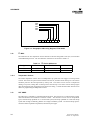
JTAG/COP SUPPORT
The MPC8240 provides a Joint Test Action Group (JTAG) interface. Additionally, the JTAG interface
is also used for accessing the common on-chip processor (COP) function of PowerPC processors. The
COP function of PowerPC processors allows a remote computer system (typically a PC with dedicated
hardware and debugging software) to access and control the internal operations of the processor. The
COP interface connects primarily through the JTAG port of the processor. The 16 pin COP header
(sample part is Samtec # HTSW-108-07-S-S) is located at J5. The COP header adds many benefits
including breakpoints, watchpoints, register and memory examination/modification and other standard
debugger features. The COP header definition is shown in Table 3-3. The location of pin 1 on the
header is indicated by the “cut-off” outline corner, which is shown diagonally across from the J5
designer in the silk screen, as in Figure 3-3.
3-4
CPCI-812 User’s Manual
Revision 1.0, August 2000
HARDWARE
.
Figure 3-3. JTAG/COP Header Orientation
Table 3-3. JTAG/COP PIN ASSIGNMENT
3.11
Signal
Pin
Pin
Signal
TDO
1
2
QACK#
TDI
3
4
TRST#
Pull-up to +3V
5
6
+3V
TCK
7
8
CHKSTOPIN#
TMS
9
10
N/C
SRESET#
11
12
GND
COP_RESET#
13
14
N/C
Pull-Up to +3V
15
16
GND
GEOGRAPHIC ADDRESSING
CompactPCI backplanes that support 64-bit connector pin assignments are required to provide a unique
differentiation based upon which physical slot the board has been inserted. The CPCI-812 makes this
definition available to the software. The definition for GA[4:0] is shown in Figure 3-4.
CPCI-812 User’s Manual
Revision 1.0, August 2000
3-5
HARDWARE
GA0
GA1
GA2
GA3
GA4
7
6
5
4
3
2
1
0
Figure 3-4. Geographic Addressing Register, FF60 0000H.
3.12
I2 C BUS
The CPCI-812 has two temperature sensors attached to the Inter-Integrated Circuit (I 2 C) bus interface
of the MPC8240 processor. The I 2C addresses of the devices are shown in Table 3-4.
Table 3-4. I2 C Device Addresses
3.12.1
Designator
Device
Function
Address
U34
LM75
Temperature Sensor
1001000
U35
LM75
Temperature Sensor
1001001
Temperature Sensors
The LM75 temperature sensors have overtemperature trip points that will trigger an interrupt when
crossed. The sensors are placed on the board at U34 and U35, and share serial interrupt #5. The sensors
should be placed in the interrupt mode by startup code. The sensors can be read for a temperature
reading at any time; reading after an interrupt clears the interrupt. The sensor will not interrupt again
until the temperature has dropped below the hysteresis setting. Consult the LM75 data sheet for more
details on programming the temperature sensors.
3.13
HOT SWAP
The CPCI-812 is a PICMG 2.1 compliant Hot Swap board. The CPCI-812 is a “Full Hot Swap” board,
with both Hardware and Software Connection control. The CPCI-812 can be used on all platform
types; Non-Hot Swap platform for a conventional system, Hot Swap platform for a Full Hot Swap
system and on High Availability platform for a High Availability system. See the Hot Swap specification for further explanation of platform, board and system types.
3-6
CPCI-812 User’s Manual
Revision 1.0, August 2000
HARDWARE
3.13.1
Hot Swap Extraction Process
Removal of the CPCI-812 in a Full Hot Swap or High Availability system is the same. The operator
first only opens the ejector handles of the board. A switch on the CPCI-812 signals to the system that it
is to be extracted. In response, the system will illuminate the blue Hot Swap LED when extraction is
permitted.
3.13.2
Hot Swap Insertion Process
Insertion of the CPCI-812 is the same in any Hot Swap system. The operator slides the CPCI-812 into
the desired slot and latches the handles.
3.14
DS1 CONNECTOR
The CPCI-812 uses a shielded RJ48C connector for the DS1 line interface. Table 3.5 lists the pin
connections and the signal description.
Table 3-5. DS1 Connector
K
PIN
SIGNAL
DESCRIPTION
1
RX-R0
Receive Ring 0
2
RX-T0
Receive Tip 0
4
TX-R0
Transmit Ring 0
5
TX-T0
Transmit Tip 0
11
RX-R1
Receive Ring 1
12
RX-T1
Receive Tip 1
14
TX-R1
Transmit Ring 1
15
TX-T1
Receive Tip 1
Note
Pin 3, 6, 7, 8, 13, 16, 17, 18, 19, and 20 are not connected.
3.15
BOARD ID REGISTER
The Board ID Register is a read-only register that can be used to differentiate between the CPCI-812
and other Cyclone Microsystems MPC8240-based CompactPCI cards. It is located at address
FF70 0000h on all such cards, with each card returning a unique ID value. Figure 3-5 shows the board
ID for the CPCI-812.
Read Only
7
6
5
1
0
0
1
0
4
3
2
1
0
Figure 3-5. Board Identification Registers, FF70 0000h
CPCI-812 User’s Manual
Revision 1.0, August 2000
3-7
HARDWARE
3-8
CPCI-812 User’s Manual
Revision 1.0, August 2000
CHAPTER 4
ATM PROGRAMMING INFORMATION
4.1
INTRODUCTION
The Control Memory, the T1XC registers and the SUNI-PDH registers are accessed through the ATMSAR. The Control Memory, the T1XC and the SUNI-PDH are accessed using the COMMAND
REGISTER (CMR), COMMAND EXTENSION REGISTER (CER) and the INDIRECT ACCESS
COMMAND of the ATM-SAR.
The INDIRECT ACCESS COMMAND has a two bit field that indicates the target of the access;
Control Memory (00), ATM-SAR registers (01), PHY device (11). The PHY device target should be
used to access both the T1XC registers and the SUNI-PDH registers. The T1XC registers have an offset
of 100h; the SUNI-PDH registers reside at 000h through 074h.
Table 4-1. Secondary Address Map for ATM-SAR Registers
CPCI-812 User’s Manual
Revision 1.0, August 2000
ATM-SAR Registers
ATM-SAR Offset
GMR
00h
GSR
04h
IMR
08h
RQU
0ch
RQA
10h
ADDR
14h
VER
18h
SWR
1ch
CMR
20h
CMR_L
24h
CER
28h
CER_L
2ch
MSH0
40h
MSH1
44h
MSH2
48h
MSH3
4ch
MSL0
50h
MSL1
54h
MSL2
58h
MSL3
5ch
MBA0
60h
MBA1
64h
MBA2
68h
MBA3
6chh
MTA0
70h
4-1
ATM PROGRAMMING INFORMATION
4.2
MTA1
74h
MTA2
78h
MTA3
7ch
MWA0
80h
MWA1
84h
MWA2
88
MWA3
8ch
DEVICE REGISTRES
The ATM-SAR, SUNI-PDH and T1XC are very flexible devices, and therefore have many registers
that can be setup to customize device operation. The following three sections identify register settings.
4.2.1
ATM-SAR Mode Registers
The ATM-SAR device has a mode register that configures the device for various modes of operation.
Almost all of the bit settings for the mode registers have already been determined and fixed by the
hardware design.
Table 4-2 shows the bit settings for the ATM-SAR mode register. Entries of “D” under “Val” indicate
that the entry is a don’t care; the bit can be set to zero or one. An “S” under “Val” means that the user
can set this for his application. Consult the ATM-SAR Chipset User’s Manual for more information.
Table 4-2. ATM-SAR General Mode Register
4-2
Bit#
Value
Name
Status/Function
0
S
RE
Receiver Enable/Disable
1
S
SE
Transmitter Enable/Disable
2
S
DR
Receive Drop Mode
3
0
BPE
Bus Parity Disabled
4
D
PC
Bus Parity Disabled
5
D
PM
Bus Parity Disabled
6
0
BO
Little endian Byte Ordering
7
0
AD
Burst Size Determined from Address
8
1
SZ
2 Word Bursts Enabled
9
1
SZ
4 Word Bursts Enabled
10
1
SZ
8 Word Bursts enabled
11
1
SZ
16 Word Bursts Enabled
12
0
RA
Read RDY Mode Normal
13
0
WA
Write RDY Mode Normal
CPCI-812 User’s Manual
Revision 1.0, August 2000
ATM PROGRAMMING INFORMATION
14
S
LP
Normal/Loopback Mode
15
0
CPE
Control Memory Parity Disabled
16-29
0
----
Reserved
30
1
SLM
Sets Registers to Word Boundaries
31
1
----
Set to 1 for Proper Operation
4.2.2
SUNI-PDH REGISTERS
The registers listed in Table 4-3 have been modified from their power-up, reset default values. In
general the SUNI-PDH is setup for direct cell mapping, HEC cell delineation and no payload
scrambling as required by the ATM Forum DS1 Physical Layer Specification. All interrupts are
disabled and loopback modes are not enabled. Also see the SUNI-PDH manual section "Basic
Operating Modes."
Table 4-3. SUNI-PDH Non-Default Register Settings
ADDR
DATA
000h
08h
Register name and Description
SUNI_PDH Configuration
Setting the FRMRBPP bit (bit3) bypasses the DS3/E3 framer.
SPLR Configuration
028h
80h
Setting the FROM [1:0] bits (bits 7,6) to [1,0] selects DS1 framing format
and clearing the PLCPEN bit (bit 2) disables the PLCP framing function of
the SMDS PLCP Layer Receiver Block.
SPLT Configuration
02Ch
80h
Setting the FORM[1:0] bits (bits 7,6) to [1,0] selects DS1 framing format
and clearing the PLCPEN bit (bit 2) disables the PLCP framing function of
the SMDS PLCP Layer Transmitter block.
RXCP Control
040h
28h
Setting the HCSADD bit (bit 5) enables the addition of the coset
polynomial to the received HCS octet before comparison with the
calculated result.Clearing the DSCR bit (bit 3) disables the payload
descrambling function.Setting the BLOCK bit(bit3) blocks Idle/
Unassigned cells from the receiver FIFO.
RXCP Framing Control
041h
01h
Setting the DELIN bit (bit0) enables the ATM cell
Delineator (ATMF) Block.That is, HEC based cell delineation is enabled.
046h
01h
RXCP Idle/Unassigned Cell Pattern:H4 octet Setting the receive idle/
unassigned cell pattern for the H4 octet to 01h causes idle cells to be
filtered and clearing to 00h causes unassigned cells to be filtered, if the
mask pattern for the H4 octet is configuring to look at all bits in the octet.
See the setting of the RXCP Idle/Unassigned Cell Mask:H4 octet
(ADDR=04Ah).
047h
FFh
RXCP Idle/Unassigned Cell Mask: H1 octet
048h
FFh
RXCP Idle/Unassigned Cell mask: H2 octet
CPCI-812 User’s Manual
Revision 1.0, August 2000
4-3
ATM PROGRAMMING INFORMATION
RXCP Idle/Unassigned cell Mask: H3 octet
049h
FFh
Setting the receive idle/unassigned cell mask for the H1, H2 and H3
octets to FFh causes all bits in all three octets to be compared with their
corresponding RXCP Idle/Unassigned Cell Patterns.
RXCP Idle/Uassigned Cell Mask:H4 octet
Setting the receive idle/unassigned cell mask for the octet to Feh cause
all bits except bit 0 of the H4 octet to be compared with their corresponding RXCP Idle/Uassigned Cell pattern. With this setting, both idle
cells(H4=01h) and unassigned cells (H4=00h) get filtered from the
receive FIFO.
04h
FEh
04F
FFh
RXCP User Idle Frame Filter
050
FFh
RXCP User Idle Frame Filter
051
FFh
RXCP User Idle Frame Filter
052
FFh
RXCP User Idle Frame Filter
TXCP Control
058H
A0h
Setting the HCSADD bit (bit5) enables the addition of the coset
polynomial to the HCS octet before transmission. Clearing the SCR bit
(bit 2) disables the payload scrambling function. Setting the HCSINS bit
(bit7) forces the calculated HCS to overwrite the HCS octet, that is the
SUNI_PDH generates and inserts the HCS.Clearing the FIFODP [1:0]
bits (bits 4,3) sets the transmit FIFO depth to 4 cells.
TXCP Interrupt Enable/Status
059h
01h
Setting the TFULL4 bit(bit4) sets the TFIFOFB/TCA pin to behave as an
“almost full” indication. This was found to work best with the ATM_SAR.
TXCP Idle/Unassigned Cell Pattern: H4 octet
05Dh
01h
Setting the transmit idle/unassigned cell pattern for the H4 octet to 01h
Causes idle cells to be generated. Clearing it to 00h causes unassigned
cells to be generated.
TXCP Idle/Uassigned Cell Pattern: H5 octet
05Eh
52h
Setting the transmit idle/unassigned cell pattern for the H5 octet to 52h is
the correct HCS for idle cells.
Setting the H5 octet to 55h is the correct HCS for unassigned cells.
TXCP Idle/Unassigned Cell Payload
05Fh
4.2.3
6Ah
Setting the transmit idle/unassigned cell payload to 6Ah is the correct
value for idle or unassigned cells.
T1XC Registers
The registers listed in the Table 4-4 have been modified from their power-up, reset default values. The
T1XC is setup for 24 frame Extended Superframe Format (ESF) and Bipolar 8 Zero Substitution
(B8ZS) line coding as required by the ATM Forum DS1 Physical Layer Specification. All interrupts are
disabled. Loopback modes are not enabled. Also see the T1XC manual section “Configuring the T1XC
from Reset.”
4-4
CPCI-812 User’s Manual
Revision 1.0, August 2000
ATM PROGRAMMING INFORMATION
Table 4-4. T1XC Non-Default Register Settings
ADDR
DATA
Register Name and Description
T1XC Receive Options
100h
103h
114h
20h
Setting the ELSTBYP bit(bit5) bypasses the elastic store block of the
T1XC, keeps the data synchronized to the recovered clock (RCLKO) and
eliminates the need for a BRCLK.
40h
T1XC Receive DS1 Interface Configuration Setting the SDOEN bit (bit 6)
forces the multifunction (input/output) pins SDP/RDP/RDD and SDN. RDN/
RLCV to outputs, eliminating the need for support of the multifunction pins
as digital inputs.
50h
XPLS Line Length Configuration setting the SM bit (bit6) and clearing the
ILS [2:0] bits (bits 2, 1, 0) sets the Analog DSX-1 Pulse Generator block to
use waveform template corresponding to a line length of 0 to 100 feet. For
longer line lengths, SM is kept to a one, and the value of FMS[1:0] is
changed. See the T1XC manual for more information.
FRMR Configuration
120h
10h
Setting the ESF bit (bit 4) and clearing FMS [1:0] (bits 3, 2) sets the Framer
for ESF framing format and 4Kbit FDL data rate. For other FDL data rates,
ESF is kept to a one, and the value of FMS [1:0] is changed. See the T1XC
manual for more information.
ALMI Configuration
12Ch
10h
130h
02h
13Eh
08h
Setting the ESF bit (bit 4) sets the Alarm Integrator for ESF framing format
and clearing FMS [1:0] (bits 3, 2) matches the settings in register 120h. For
other FDL data rates, ESF is kept to a one, and the value of FMS [1:0] is
changed. See the T1XC manual for more information.
TPSC Configuration
The T1XC manual says to set the IND bit (bit 1) for proper operation.
IBCD Activate Code
The T1XC manual says to set the activate loopback to 08h for ESF frame
format operation.
IBCD Deactivate Code
13Fh
44h
The T1XC manual says to set the deactivate loopback code to 44h for ESF
frame format operation.
SIGX Configuration
140h
12h
Setting the ESF bit (bit4) selects ESF framing format clearing FMS [1:0]
(bits 3, 2) matches the settings in registers 120h and 12Ch. The T1XC
says to see the IND bit (bit 1) for proper operation.
XBAS Configuration
144h
30h
150h
02h
CPCI-812 User’s Manual
Revision 1.0, August 2000
Setting the ESF bit (bit 4) selects ESF framing format and clearing FMS
[1:0] (bits 3, 2) matches the settings in registers 120h, 12Ch and 140h.
Setting the B8ZS bit (bit 5) selects B8ZS line coding.
RPSC Configuration
The T1XC manual says to set the IND bit (bit 1) for proper operation.
4-5
ATM PROGRAMMING INFORMATION
4.3
SOFTWARE RESET
All six VLSI devices (2 ATM-SARs, 2 SUNI-PDHs and 2 T1XCs) can be reset by software. The
actions required to reset the devices follow and the equivalent of asserting their respective reset pins.
4.3.1
ATM-SARs Software Reset
The ATM-SAR is reset when any value is written to the software reset register at offset 0000 001Ch.
4.3.2
SUNI-PDHs Software Reset
The SUNI_PDH is reset when 0x08h (or any other value that sets bit 7 to a one) is written to the Identification and Master Reset Register at offset 0x04h. The SUNI-PDH will remain reset until a 0x00h (or
any other value that clears bit 7 to a zero) is written to offset 0x04h.
4.4
LOOPBACK
The ATM-SAR, SUNI-PDH, and T1XC each has one loopback path.
Loopback paths within the ATM-SARs is performed by setting the LP bit (bit 14) of the ATM-SAR’s
General Mode Register. A multiplexer internal to the ATM-SAR allows data to traverse the entire
transmit and receive data paths of the ATM-SAR. See the ATM-SAR User’s Manual for more
reference.
The diagnostic loopback of the SUNI_PDH is obtained by setting the DLB bit (bit 2) of the SUNIPDH’s Configuration Register (0x00h). Like the ATM-SAR loopback, the diagnostic loopback
connects the transmit data to the receive data, allowing data to traverse the transmit and receive data
paths of the SUNI-PDH.
Like the loopbacks for the ATM-SAR and SUNI-PDH, the two loopback modes available in the T1XC
connect transmit data to receive data. The diagnostics digital loopback is enabled by setting the DDLB
bit (bit 2) of the T1XC Master Diagnostics register (0x10Ah). This mode loops transmit data to receive
data, but does not include the analog drivers of the T1XC. The diagnostic metallic loopback is enabled
by setting the DMLB bit (bit 3) of the T1XC Master Diagnostics register (0x10Ah). This mode loops
transmit data to receive data just after the analog drivers of the T1XC.
4.5
CLOCKING OPTIONS
In normal operation, the transmit clock is derived from the receive data. Loop timing is enabled by
setting the LOOPT bit (bit 4) of the SUNI-PDH Configuration Register (0x000h).
4-6
CPCI-812 User’s Manual
Revision 1.0, August 2000
CHAPTER 5
pSOS SOFTWARE DEVELOPMENT
5.1
INTRODUCTION
This chapter is dedicated to aiding pSOS application development using the Cyclone CPCI-812 pSOS
BSP. It contains information specific to the Cyclone BSP, and is intended to be used in conjunction
with the pSOS documentation provided by ISI / Wind River Systems. Note that there are many items
within the BSP that a user may want to self configure, so users should be readily able to modify and
rebuild the BSP when necessary.
Once an application has been built and linked with the CPCI-812 BSP, the image can be downloaded to
DRAM via Ethernet using the Cyclone TFTP Bootloader (see accompanying documentation on this
procedure), or downloaded to Flash ROM or DRAM using a JTAG-emulator such as Wind River’s
Visionprobe tool (see section 3.10).
This chapter is divided into the following sections:
5.2
•
Embedded Utilities Memory Block
•
Endian Considerations
•
PCI Configuration
•
EPIC Interrupt Programming
•
LM75 Temperature Sensors
EMBEDDED UTILITIES MEMORY BLOCK
The Embedded Utilities Memory Block (EUMB) is a relocatable memory block that contains the
registers for several of the MPC8240’s embedded features, including the Messaging Unit, DMA
Controller, Address Translation Unit (ATU), I2C Controller, and Embedded Programmable Interrupt
Controller (EPIC). Figure 5-1 shows the EUMB memory offsets for each of these embedded devices.
The base of the EUMB is software programmable by setting the EUMB Base Address Register
(EUMBBAR) in the MPC8240’s PCI Configuration Space (offset 0x78). pSOS initialization sets this
value at startup. Users should never modify this value, and should read this value when necessary using
a local PCI configuration read cycle (see section 5.4).
For further information on MPC8240 address maps and the EUMB, consult chapter 4 of the MPC8240
User’s Manual.
CPCI-812 User’s Manual
Revision 1.0, August 2000
5-1
pSOS SOFTWARE DEVELOPMENT
0x0 0000
0x0 1000
0x0 2000
0x0 3000
Message Unit
DMA
ATU
I 2C
0x0 4000
0x4 0000
EPIC
0x8 0000
0xF FFFF
Shaded area indicates locations not
allowed for the EUMB
Figure 5-1. Embedded Utilities Memory Block
5.3
ENDIAN CONSIDERATIONS
The MPC8240 on the CPCI-812 stores data in local memory in a big endian manner (most significant
byte in the lowest memory address). However, the PCI bus is a little endian bus (least significant byte
in the lowest byte lane), including access to all registers in the EUMB. Care must be taken to byte swap
data transferred from memory to the PCI bus or EUMB registers.
pSOS provides the following functions to read and write data to/from the PCI bus and EUMB. They
perform all required byte swapping. The following function declarations are from pci/pcihdr.h:
void PciWrite32(ULONG addr, ULONG value);
void PciWrite16(ULONG addr, ULONG value);
void PciWrite8 (ULONG addr, ULONG value);
ULONG PciRead32(ULONG addr);
ULONG PciRead16(ULONG addr);
ULONG PciRead8(ULONG addr);
5.4
PCI CONFIGURATION
There are two PCI buses on the CPCI-812. The CompactPCI bus interconnects the CPCI-812 with the
CompactPCI host and the other IOP cards in the system. The local PCI bus connects the MPC8240 with
the PLX PCI-9080, allowing access to the NEC SAR devices.
5-2
CPCI-812 User’s Manual
Revision 1.0, August 2000
pSOS SOFTWARE DEVELOPMENT
The two buses are interconnected via the Intel 21554 embedded PCI-to-PCI bridge. The primary side of
this bridge is connected to the CompactPCI bus, and the secondary side is connected to the MPC8240
PCI bus. Because the 21554 is an embedded bridge (non-transparent), PCI configuration cycles are not
forwarded through it. The device has two configuration spaces, one for the primary side, one for the
secondary. Therefore the CompactPCI host is responsible for configuring the primary side of the
bridge, and the MPC8240 is responsible for configuring the secondary side of the bridge, as well as the
PLX-PCI9080 resident on the local PCI bus.
5.4.1
Downstream (Inbound) CompactPCI Transactions
PCI BIOS software on the CompactPCI host is responsible for configuring the embedded bridge for
inbound PCI transactions. However, the MPC8240 must first pre-configure the device while the host’s
configuration cycles are being retried. Preconfiguration of downstream PCI memory window 0 allows
the host to assign a CompactPCI address to the CPCI-812 in Base Address Register 2 of the bridge that
will translate to a valid PCI address on the local PCI bus.
This preconfiguration includes setting the PCI memory size request to the size of DRAM (64 MBytes),
and setting the translation value to 0x00000000. Once the preconfiguration is complete, the retry
condition is cleared on the bridge, allowing the host to assign a CompactPCI address range to the
device. As a result, all inbound PCI transactions claimed by the bridge are forwarded onto the local PCI
bus, where it is claimed by the MPC8240 and mapped to its respective address in DRAM.
As configured, after system initialization, the CompactPCI host or any other IOP card in the system can
perform a PCI memory read or write to the 64 Mbytes that starts at the value stored in Base Address
Register 2 of the embedded bridge. This transaction will be translated to a local memory read or write,
with the base address mapping to DRAM address 0x00000000.
5.4.2
Upstream (Outbound) CompactPCI Transactions
Preconfiguration of the embedded bridge also sets the size and remap address of upstream PCI memory
window 0. This window can be used to transfer data over the CompactPCI bus from the MPC8240 to
the host or other IOP cards. The size, by default, is set to 64 MBytes, and the remap value is set to
0x00000000, which in most PCI systems is allocated to the PCI host card.
Once preconfiguration is complete, the embedded bridge is configured by the MPC8240 when it runs
the pSOS PCI Auto-Configuration suite. This creates a 64 MBytes window, mapped onto the
CompactPCI bus, whose base address can be read from Base Address Register 2. Changing the remap
translation value for this memory space in the bridge allows this 64 MBytes window to be mapped to a
different region on the CompactPCI bus.
5.4.3
PLX PCI9080 Configuration
The PLX PCI9080 is a PCI-to-local bus bridge chip. Its purpose on the CPCI-812 is to interface the
local PCI bus with the ATM SAR devices. Configuration of the device allows PCI cycles claimed by
the PLX PCI9080 to be forwarded, with translation, through to the local bus, where they are claimed by
one of the two SAR devices.
CPCI-812 User’s Manual
Revision 1.0, August 2000
5-3
pSOS SOFTWARE DEVELOPMENT
Because there are two SAR devices on the CPCI-812, two PCI regions are required, one for each
device. pSOS configuration sets up the PCI9080 to request two 1 MByte PCI memory regions. As
shown in Table 5-1, PCI9080 Base Address 2 is used to access the registers on SAR0, and Base Address
3 is used to access SAR1.
User software should read these base address registers and add the appropriate SAR register offset to
create a pointer to a particular SAR register. Register offsets on the CPCI-812 are incremented by 4
bytes. For example, to create a pointer to the SAR General Status Register on Unit 1, one would read
the value of Base Address 3 on the PCI9080 device and add to it the GSR offset, 0x04.
Note that PCI9080 configuration places the device into Big Endian mode. Therefore, no endian
conversions are necessary when accessing the SAR registers (direct or indirect), despite the fact that the
PCI bus is little endian. However, accessing the memory-mapped registers on the PCI9080 does
require a big-to-little endian byte swap before writing or after reading.
Table 5-1. PLX PCI9080 Base Address Registers on CPCI-812
5.4.4
Base Address
Register
Size
Requested
Function
PCIBAR0
0x100000
PCI Base Address to access memory-mapped
PCI9080 Configuration Registers.
PCIBAR1
0x100000
PCI Base Address to access I/O-mapped
PCI9080 Configuration Registers.
PCIBAR2
0x100000
PCI Base Address to access SAR Unit 0, region
is translated to 0xC00xxxxx on the local bus.
PCIBAR3
0x100000
PCI Base Address to access SAR Unit 1, region
is translated to 0xC80xxxxx on the local bus.
Changing PCI Configuration
PCI memory or I/O size requests must be configured before PCI initialization occurs, be it on the
CompactPCI or local PCI bus. Therefore any required changes to the default PCI configuration
described above must be done in the BSP file pcicfg.c. All PLX PCI9080 pre-PCI configuration occurs
in the function preconfig_9080, and all pre-PCI configuration on the 21554 embedded bridge device
occurs is preconfig_21554.
For further information on PCI configuration, consult the Intel 21554 Embedded PCI-to-PCI data sheet,
the PLX PCI9080 data sheet, chapter 8 of the MPC8240 User’s Manual, and chapter 6 of the pRISM+
Advance Topics Guide.
5.4.5
pSOS PCI Device Driver Interface
The CPCI812 BSP uses pSOS PCI Auto-Configuration to configure the PCI devices on the local PCI
bus. This procedure creates and maintains a list of PCI information in a PCI device list. Thus device
driver developers can use any of the functions described in chapter 6 of the pRISM+ Advance Topics
Guide to find, claim, or access either the embedded bridge or the PCI9080, and thus the SCA devices.
In addition, the PCI header file (\pci\pcihdr.h) provides useful prototypes and important macros for
dealing with PCI devices.
5-4
CPCI-812 User’s Manual
Revision 1.0, August 2000
pSOS SOFTWARE DEVELOPMENT
One important definition in this header file is the PCI_LOC structure, which is used to define the PCI
location of a particular device. This structure is defined below in Figure 5-2. At PCI configuration, a
list of PCI_LOC structures is created by the pSOS Auto-Configuration. This list is defined in pcicfg.c
by:
PCI_LOC
pci_dev_list[PCI_DEV_LIST_SIZE];
This list is important, as it contains a PCI_LOC structure for all of the PCI devices on the local PCI bus.
Many pSOS PCI functions, such as those to find a particular device in the list, require a pointer to this
list and the list length as arguments. Others, such as those that access a particular PCI device, require
the PCI_LOC element from the list, which indicates which device the transaction is to occur on.
typedef struct pciloc {
short
bus;
char
device;
char
function;
char
hostBridge;
unsigned char cfgFlags;
unsigned char claimed;
unsigned char cfgStat;
unsigned long dev_vend;
unsigned long keyValue;
unsigned long intrVec;
} PCI_LOC;
/*
/*
/*
/*
/*
/*
/*
/*
/*
/*
bus number */
device number */
function number */
Host/PCI bridge number*/
Configuration flags */
Claimed Status */
Configuration Status */
Devices and Vendor ID */
pSOS Key Value */
Interrupt vector number */
Figure 5-2. PCI_LOC Structure Definition
5.5
EPIC INTERRUPT PROGRAMMING
The Embedded Programmable Interrupt Controller (EPIC) is the general-purpose interrupt controller
internal to the MPC8240. EPIC control and status registers are located in the EUMB.
CPCI-812 hardware is configured to provide nine dedicated external hardware interrupts, which are
time-division multiplexed onto one serial input on the MPC8240. The EPIC controller also provides
four internal timers that can be interrupt sources, and handles internal interrupts from the I 2C, I 2O, and 2
DMA channels.
Table 5-2 shows the EPIC hardware interrupts, and the assigned default interrupt priorities. These
interrupt priorities can be modified by the application programmer by changing the vector priority
values in the table called priTable_812 in the BSP file epic.c, and recompiling the BSP. Priority values
are in the range of 15 to 0, with 15 being the highest priority (0 inhibiting the interrupt altogether).
For further information on the MPC8240 EPIC, consult chapter 4 of the MPC8240 User’s Manual.
CPCI-812 User’s Manual
Revision 1.0, August 2000
5-5
pSOS SOFTWARE DEVELOPMENT
Table 5-2. CPCI-812 Interrupt Vectors
5.5.1
INT
NUMBER
INT
VECTOR
SOURCE
PRIORITY LEVEL
DESCRIPTION
0
0x10
MIC_INTB
1
INTB on PCI Bus
1
0x11
MIC_INTA
1
INTA on PCI Bus
2
0x12
SAR1_INT
7
Interrupt from SAR Unit 1
3
0x13
SAR0_INT
7
Interrupt from SAR Unit 0
4
0x14
UART_INT
8
UART Interrupt
5
0x15
TEMP_INT
6
LM75 Temperature Interrupt
6
0x16
LSERR
0
LSERR interrupt from PCI9080
7
0x17
SINTA
0
SINTA interrupt from PCI9080
8
0x18
MIC_INTD
1
INTD on PCI Bus
9
0x19
MIC_INTC
1
INTC on PCI Bus
10
0x1a
UNUSED
0
UNUSED
11
0x1b
UNUSED
0
UNUSED
12
0x1c
UNUSED
0
UNUSED
13
0x1d
UNUSED
0
UNUSED
14
0x1e
UNUSED
0
UNUSED
15
0x1f
UNUSED
0
UNUSED
16
0x20
TIMER0
12
EPIC Internal Tick Timer 0
17
0x21
TIMER1
12
EPIC Internal Tick Timer 1
18
0x22
TIMER2
2
EPIC Internal Tick Timer 2
19
0x23
TIMER3
2
EPIC Internal Tick Timer 3
20
0x24
I2 C
4
Interrupt from I2 C Controller
21
0x25
DMA0
7
Interrupt from DMA Channel 0
22
0x26
DMA1
7
Interrupt from DMA Channel 1
23
0x27
MSG_UNIT
7
Interrupt from Messaging Unit
Connecting and Disconnecting Interrupt Handlers in pSOS
PSOS utilities for connecting and disconnecting interrupt handlers to these interrupts can be found in
the BSP file isr.c. The function PssSetIntHandler is used to connect and enable an interrupt handler:
long PssSetIntHandler(
ULONG Level,
void *handler,
void *arg,
ULONG type
/* Interrupt vector number */
/* Pointer to handler function */
/* Optional argument to handler */
/* Optional wrapper type */
)
5-6
CPCI-812 User’s Manual
Revision 1.0, August 2000
pSOS SOFTWARE DEVELOPMENT
The function PssUnSetIntHandler is used to disconnect an interrupt handler:
long PssUnSetIntHandler(
ULONG Level,
/* Interrupt vector number */
void *handler,
/* Pointer to handler function */
void *arg
/* Optional argument to handler */
)
5.6
LM75 TEMPERATURE SENSORS
The two on-board LM75 devices can be used to detect possible temperature problems in the system,
such as overheating. The BSP file lm75.c contains a collection of routines that simplify the use of the
devices. Included are functions to read and write to registers on the LM75, including the temperature,
trip, and hysteresis registers.
Before use, the LM75 should be placed in interrupt mode. When in this mode an LM75 will interrupt if
the temperature goes above the value in the trip register, and will interrupt again when the temperature
falls back below the value in the hysteresis register.
Also included in the lm75.c file is the function lm75_test, which is a simple diagnostic that uses useful
LM75 routines to test the devices. Developers can use this as an example for writing their own utilities
to operate the LM75, and can also call this test in their application to ensure that the devices are
operating correctly.
For further information consult the National Semiconductor LM75 Data Sheet.
CPCI-812 User’s Manual
Revision 1.0, August 2000
5-7
APPENDIX A
PCI LOCAL BUS SIGNALS
A.1
INTRODUCTION
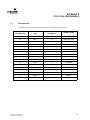
The following tables list the PCI Local Bus signals on AMP Mictor-38 connectors.
CYCLONE
MICTOR PIN #
ANALYSIS PROBE
POD
LOGIC ANALYZER
CHANNEL #
SIGNAL NAME
36
POD 1
CLK/16
SPERR#
35
POD 1
15
SSBO(not used)
34
POD 1
14
SSERR#
33
POD 1
13
SPAR
32
POD 1
12
C/BE1
31
POD 1
11
C/BE0
30
POD 1
10
ACK64#
29
POD 1
9
REQ64#
28
POD 1
8
SC/BE7#
27
POD 1
7
SC/BE6#
26
POD 1
6
SC/BE5#
25
POD 1
5
SC/BE4#
24
POD 1
4
SPAR64
23
POD 1
3
USER5
22
POD 1
2
USER4
21
POD 1
1
USER3
20
POD 1
0
USER2
CPCI-812 User’s Manual
Revision 1.0, August 2000
A-1
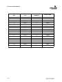
PCI LOCAL BUS SIGNALS
A-2
CYCLONE MICTOR
PIN #
ANALYSIS PROBE
POD
LOGIC ANALYZER
CHANNEL #
SIGNAL NAME
3
POD 3
CLK/16
USER1
4
POD 3
15
SAD15
5
POD 3
14
SAD14
6
POD 3
13
SAD13
7
POD 3
12
SAD12
8
POD 3
11
SAD11
9
POD 3
10
SAD10
10
POD 3
9
SAD09
11
POD 3
8
SAD08
12
POD 3
7
SAD07
13
POD 3
6
SAD06
14
POD 3
5
SAD05
15
POD 3
4
SAD04
16
POD 3
3
SAD03
17
POD 3
2
SAD02
18
POD 3
1
SAD01
19
POD 3
0
SAD00
CPCI-812 User’s Manual
Revision 1.0, August 2000
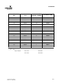
APPENDIX A
CYCLONE MICTOR
PIN #
ANALYSIS PROBE
POD
LOGIC ANALYZER
CHANNEL NUMBER
PCI SIGNAL NAME
3
POD 4
CLK/16
SCLK
4
POD 4
15
SAD31
5
POD 4
14
SAD30
6
POD 4
13
SAD29
7
POD 4
12
SAD28
8
POD 4
11
SAD27
9
POD 4
10
SAD26
10
POD 4
9
SAD25
11
POD 4
8
SAD24
12
POD 4
7
SAD23
13
POD 4
6
SAD22
14
POD 4
5
SAD21
15
POD 4
4
SAD20
16
POD 4
3
SAD19
17
POD 4
2
SAD18
18
POD 4
1
SAD17
19
POD 4
0
SAD16
K
Note
Logic Analyzer
CPCI-812 User’s Manual
Revision 1.0, August 2000
POD 1 & 3
MICTOR 1
POD 2 & 4
MICTOR 2
A-3