1
SIDSA
Semiconductor Design Solutions
FIPSOC Boot Program
Overview
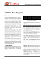
The Field Programmable System On Chip (FIPSOC)
constitutes a new concept in system integration. It
provides the user with the possibility of integrating a
microprocessor core along with programmable digital
and analog cells within the same integrated circuit.
This chip can be considered as a large granularity
FPGA with a FPAA (Field Programmable Analog
Array) and a built-in microprocessor core that does
not only act as a general purpose processing element,
but also configures the programmable cells and their
interconnections. Therefore, there is a strong
interaction between hardware and software as long as
signal values and configuration data within the
programmable
cells
are
accessible
from
microprocessor programs.
This chapter describes the program stored in internal
ROM used to boot the device from a serial stream.
The program interprets in real time an extension of
Intel's HEX records. Commands are provided for
programming internal (both directly and indirectly)
and external RAM, reading internal (both directly and
indirectly) and external RAM and code ROM, and
program branching and returning. SFRs can then be
accessed this way as long as direct writes to the
internal memory can be done.
The extended HEX records are taken either from the
RS-232 serial port (typically coming from a PC) or
from a serial memory (typically flash or E2PROM)
supporting SPI or 2-wire protocols. RS-232 and SPI
modes also support reading, so the whole chip can be
controlled (programmed and read) using a single
serial link (typically from a PC).
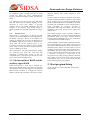
1. Boot modes
FIPSOC provides four boot modes which are selected
from external pins boot1 and boot2. The address port
AD[15:8] is sampled during reset to provide extra
configuration information. Table 1 shows the four
boot modes.
Chapter 9. FIPSOC Boot Program
boot1
0
0
1
1
boot0
0
1
0
1
Boot mode
2-wire
SPI
SCI
External parallel ROM
Table 1: FIPSOC boot modes
The last FIPSOC boot mode can be read with the
special function register (SFR) SBCR located at
address $9D:
7
6
5
4
3
2
1
0
SCEN
SCSL
Master
SCIE
GOE
OD
IREN
BAUD
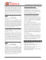
SCEN (bit 7) - Serial Communication Enable: The
serial communication system, which can be
configured either as 2-wire or SPI, is enabled if this
bit is high. Its value upon reset is the inverted value
of the external BOOT1 pin.
SCSL (bit 6) - Serial Communication Select: The
serial communication system is configured as 2-wire
if this bit is set, SPI otherwise. Its value upon reset is
the inverted value of the external BOOT0 pin.
Master (bit 5) - Boot Master: This bit stores the
serial communication mode (master or slave) upon
reset . Its value is the inverted value of bit #15 of the
address port, AD[15], and is latched during the reset
sequence.
SCIE (bit 4) - Serial Communication Interrupt
Enable: It enables the interrupt of the serial
communication system. Its reset value is zero.
GOE (bit 3) - Global Output Enable: When reset, it
disables every output of every DMC and places all
the IO pads in input state. Its reset value is zero.
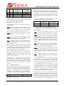
OD (bit 2) - Open Drain: The general purpose port
GPORT pins behave as open drain when configured
as outputs when this bit is set, as normal CMOS
outputs otherwise. Its reset state depends on the boot
mode: if booting from SPI (BOOT1=0 and
BOOT0=1), then OD is initialized from bit #10 of the
address port, AD[10]; if booting from 2-wire
(BOOT1=BOOT0=0), OD is initialized to 1;
otherwise, OD is initialized to zero (normal CMOS
outputs), although all bits in the data direction
register DDRP are initialized to 1 thus configuring all
port pins as inputs.
2