1
SIDSA
Semiconductor Design Solutions
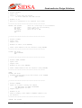
sequential memory locations of the internal data
RAM memory starting from address add_L using
indirect addressing (the add_H field is ignored but
used in the checksum). This implies that writes to
addresses ranging from 80H to FFH will be done on
data memory rather than SFRs. The number of bytes
that can be written is limited to 63, and an attempt to
write more than that will in general cause a checksum
error.
Record type 18H: Indirectly Read from internal
memory. The general syntax for this record is the
following:
:01H
<add_H><add_L>
<number_of_bytes> <checksum>
18H
Interpretation
of
this
command
reads
number_of_bytes bytes from sequential memory
locations of the internal data RAM memory starting
from address add_L using indirect addressing (the
add_H field is ignored but used in the checksum).
This implies that reads from addresses ranging from
80H to FFH will be done on data memory rather than
SFRs. Data is sent trough the serial link sequentially
as it is read. This record is not supported if 2-wire
communication mode is selected.
Record type 20H: Directly write to internal memory.
The general syntax for this record is the following:
: <number_of_bytes>
{<byte>} <checksum>
<add_H> <add_L> 20H
Interpretation
of
this
command
writes
number_of_bytes bytes specified in the byte fields in
sequential memory locations of the internal data
RAM memory starting from address add_L using
direct addressing (the add_H field is ignored but used
in the checksum). This implies that writes to
addresses ranging from 80H to FFH will be done on
SFRs rather than data memory. The number of bytes
that can be written is limited to 63, and an attempt to
write more than that will in general cause a checksum
error.
Record type 40H: Jump to address. The general
syntax for this record is the following:
:00H <add_H><add_L> 40H <checksum>
Interpretation of this command produces a direct
jump to address add_H * 256 + add_L. Depending on
the booting mode, parts of the serial link circuitry
may be powered down prior to jumping.
Record type 48H: Return from subroutine. The
general syntax for this record is the following:
:00H <add_H><add_L> 48H <checksum>
Interpretation of this command executes a "RET"
instruction, which pops the address to jump to from
the stack. It is used when the record parsing program
is used as a subroutine from an user application
program. fields add_H and add_L are ignored but
used in the checksum.
1.2.2.
Extended record types and errors
Record types 80H to FFH are available for command
set extension. If such a record type is parsed the
program jumps to address $FF2B where an
appropriate parsing routine should be found. Upon
initialization a default error routine is written there.
This error routine is entered whenever a colon is not
found at the begining of an HEX record, a checksum
is incorrect, a record type is not recognized or any
other parsing problem is detected. This routine resets
the GOE bit to place the whole programmable logic
are in an idle mode and then keeps branching to the
same address.
1.2.3.
Booting from SPI
When boot1 is 0 and boot0 is 1 during the reset
sequence, the extended HEX records are fetched from
the SPI serial link. The address port AD is also
sampled upon reset and automatically configures
several features of the SPI interface according to
external user-defined hardware settings:
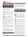
7
6
5
4
3
2
Master
CPOL
CPHA
CK1
CK0
OD
1
0
Record type 28H: Directly Read from internal
memory. The general syntax for this record is the
following:
Master (bit 7): FIPSOC will act as an SPI master if
this bit is set, slave otherwise.
:01H
<add_H><add_L>
<number_of_bytes> <checksum>
28H
CPOL (bit 6): Selects the SPI clock polarity (refer to
the SPI section of this user's manual).
Interpretation
of
this
command
reads
number_of_bytes bytes from sequential memory
locations of the internal data RAM memory starting
from address add_L using direct addressing (the
add_H field is ignored but used in the checksum).
This implies that reads from addresses ranging from
80H to FFH will be done on SFRs rather than data
memory. Data is sent trough the serial link
sequentially as it is read. This record is not supported
if 2-wire communication mode is selected.
CPHA (bit 5): Selects the SPI clock phase (refer to
the SPI section of this user's manual).
Chapter 9. FIPSOC Boot Program
CK1 and CK0 (bits 4 and 3): Select the SPI clock
frequency as shown in table 2 (refer to the SPI
section of this user's manual).
4